BLE112 Datasheet - SemiconductorStore.com Reference schematic added 0.93 Description updated 0.94...
27
BLE112 DATA SHEET Tuesday, 13 December 2011 Version 1.11
Transcript of BLE112 Datasheet - SemiconductorStore.com Reference schematic added 0.93 Description updated 0.94...
BLE112 DATA SHEET
Tuesday, 13 December 2011
Version 1.11
Bluegiga Technologies Oy
Copyright © 2000-2011 Bluegiga Technologies
All rights reserved.
Bluegiga Technologies assumes no responsibility for any errors which may appear in this manual. Furthermore, Bluegiga Technologies reserves the right to alter the hardware, software, and/or specifications detailed here at any time without notice and does not make any commitment to update the information contained here. Bluegiga’s products are not authorized for use as critical components in life support devices or systems.
The WRAP is a registered trademark of Bluegiga Technologies
The Bluetooth trademark is owned by the Bluetooth SIG Inc., USA and is licensed to Bluegiga Technologies. All other trademarks listed herein are owned by their respective owners.
Bluegiga Technologies Oy
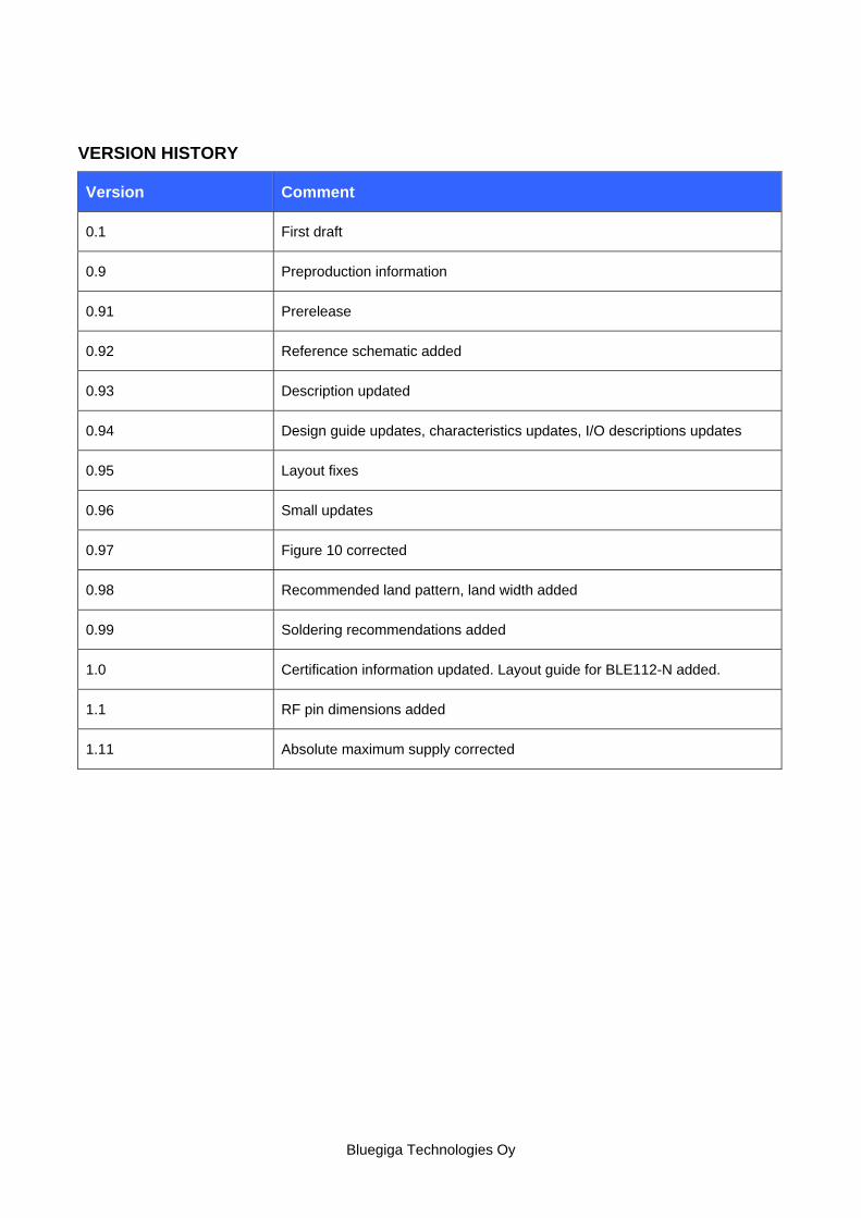
VERSION HISTORY
Version Comment
0.1 First draft
0.9 Preproduction information
0.91 Prerelease
0.92 Reference schematic added
0.93 Description updated
0.94 Design guide updates, characteristics updates, I/O descriptions updates
0.95 Layout fixes
0.96 Small updates
0.97 Figure 10 corrected
0.98 Recommended land pattern, land width added
0.99 Soldering recommendations added
1.0 Certification information updated. Layout guide for BLE112-N added.
1.1 RF pin dimensions added
1.11 Absolute maximum supply corrected
Bluegiga Technologies Oy
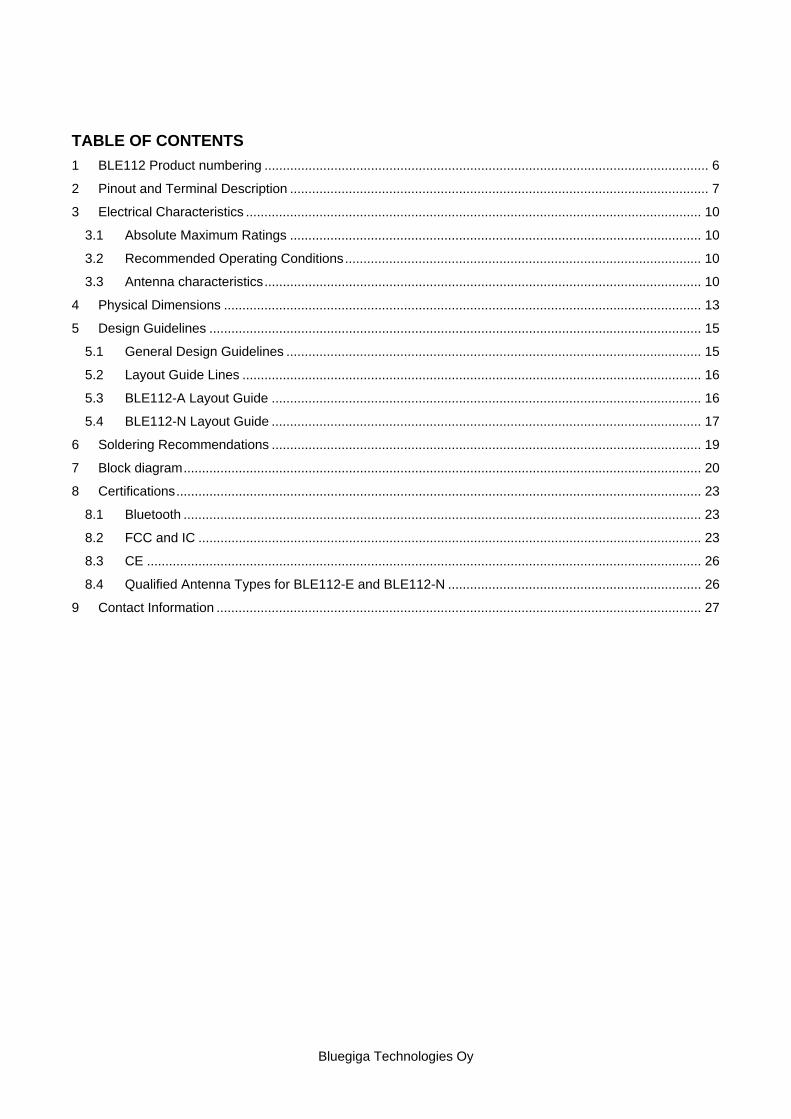
TABLE OF CONTENTS
1 BLE112 Product numbering ......................................................................................................................... 6
2 Pinout and Terminal Description .................................................................................................................. 7
3 Electrical Characteristics ............................................................................................................................ 10
3.1 Absolute Maximum Ratings ................................................................................................................ 10
3.2 Recommended Operating Conditions ................................................................................................. 10
3.3 Antenna characteristics ....................................................................................................................... 10
4 Physical Dimensions .................................................................................................................................. 13
5 Design Guidelines ...................................................................................................................................... 15
5.1 General Design Guidelines ................................................................................................................. 15
5.2 Layout Guide Lines ............................................................................................................................. 16
5.3 BLE112-A Layout Guide ..................................................................................................................... 16
5.4 BLE112-N Layout Guide ..................................................................................................................... 17
6 Soldering Recommendations ..................................................................................................................... 19
7 Block diagram ............................................................................................................................................. 20
8 Certifications ............................................................................................................................................... 23
8.1 Bluetooth ............................................................................................................................................. 23
8.2 FCC and IC ......................................................................................................................................... 23
8.3 CE ....................................................................................................................................................... 26
8.4 Qualified Antenna Types for BLE112-E and BLE112-N ..................................................................... 26
9 Contact Information .................................................................................................................................... 27
Bluegiga Technologies Oy
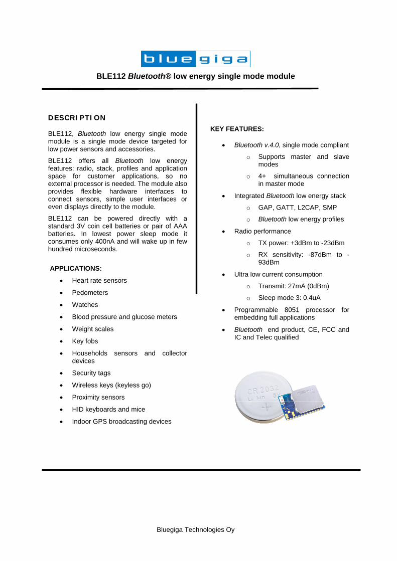
BLE112 Bluetooth® low energy single mode module
DESCRIPTION
BLE112, Bluetooth low energy single mode module is a single mode device targeted for low power sensors and accessories.
BLE112 offers all Bluetooth low energy features: radio, stack, profiles and application space for customer applications, so no external processor is needed. The module also provides flexible hardware interfaces to connect sensors, simple user interfaces or even displays directly to the module.
BLE112 can be powered directly with a standard 3V coin cell batteries or pair of AAA batteries. In lowest power sleep mode it consumes only 400nA and will wake up in few hundred microseconds.
APPLICATIONS:
Heart rate sensors
Pedometers
Watches
Blood pressure and glucose meters
Weight scales
Key fobs
Households sensors and collector devices
Security tags
Wireless keys (keyless go)
Proximity sensors
HID keyboards and mice
Indoor GPS broadcasting devices
KEY FEATURES:
Bluetooth v.4.0, single mode compliant
o Supports master and slave modes
o 4+ simultaneous connection in master mode
Integrated Bluetooth low energy stack
o GAP, GATT, L2CAP, SMP
o Bluetooth low energy profiles
Radio performance
o TX power: +3dBm to -23dBm
o RX sensitivity: -87dBm to -93dBm
Ultra low current consumption
o Transmit: 27mA (0dBm)
o Sleep mode 3: 0.4uA
Programmable 8051 processor for embedding full applications
Bluetooth end product, CE, FCC and IC and Telec qualified
Bluegiga Technologies Oy
Page 6 of 27
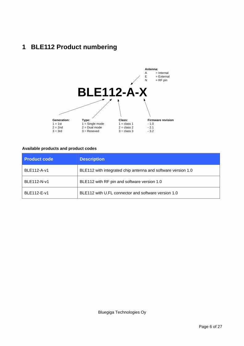
1 BLE112 Product numbering
BLE112-A-X
Generation:1 = 1st2 = 2nd3 = 3rd
Firmware revision- 1.0- 2.1- 3.2
Antenna:A = InternalE = ExternalN = RF pin
Type:1 = Single mode2 = Dual mode3 = Reseved
Class:1 = class 12 = class 23 = class 3
Available products and product codes
Product code Description
BLE112-A-v1 BLE112 with integrated chip antenna and software version 1.0
BLE112-N-v1 BLE112 with RF pin and software version 1.0
BLE112-E-v1 BLE112 with U.FL connector and software version 1.0
Bluegiga Technologies Oy
Page 7 of 27
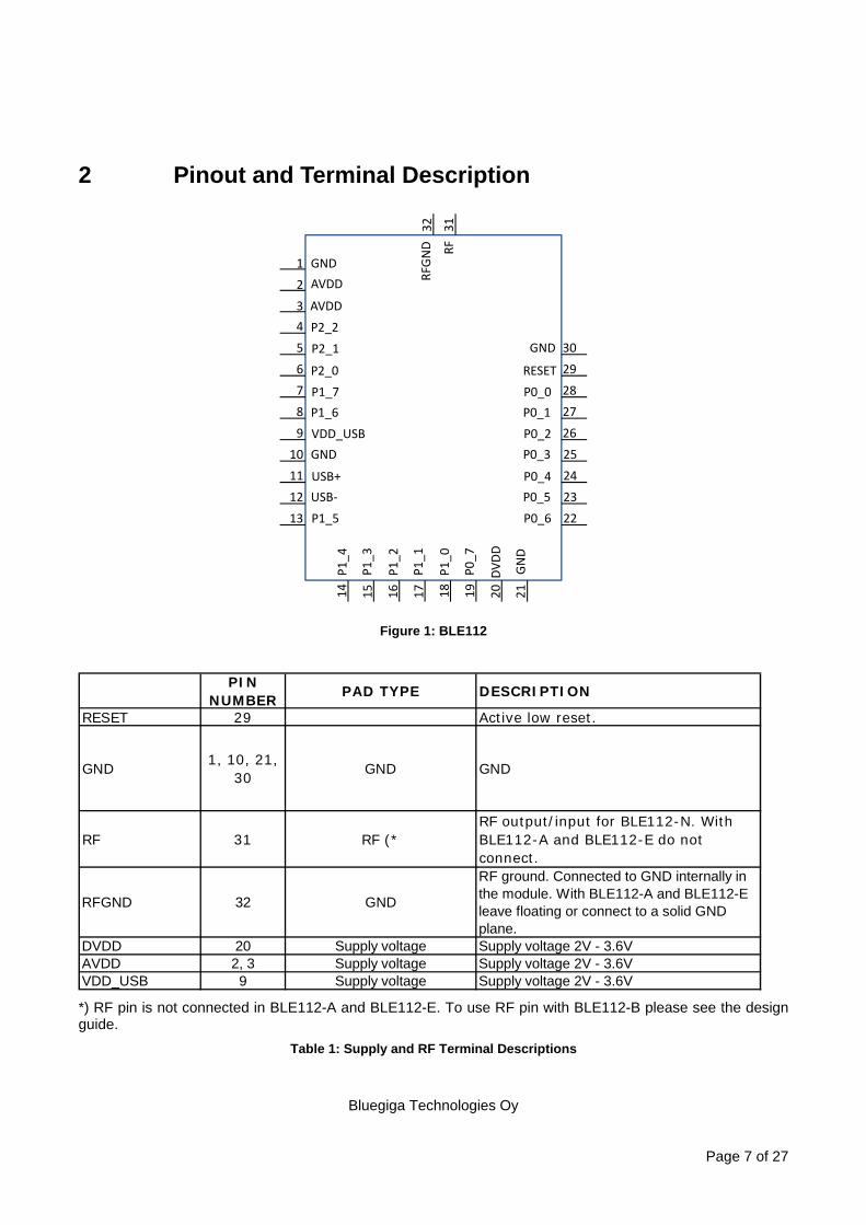
2 Pinout and Terminal Description
1
2
3
4
5
6
7
8
9
10
11
12
13
14 15 16 17 18 19 20 21
32 31
30
29
28
27
26
25
24
23
22
GND
AVDD
GND
AVDD
GN
D
GND
P2_2
P2_1
P2_0
P1_7
P1_6
VDD_USB
USB+
USB-
P1_5
DVD
D
P0_7
P1_0
P1_1
P1_2
P1_3
P1_4
P0_3
RESET
P0_0
P0_1
P0_2
P0_4
P0_5
P0_6
RF
RFG
ND
Figure 1: BLE112
PIN NUMBER
PAD TYPE DESCRIPTION
RESET 29 Active low reset.
GND1, 10, 21,
30GND GND
RF 31 RF (*RF output/input for BLE112-N. With BLE112-A and BLE112-E do not connect.
RFGND 32 GND
RF ground. Connected to GND internally in the module. With BLE112-A and BLE112-E leave floating or connect to a solid GND plane.
DVDD 20 Supply voltage Supply voltage 2V - 3.6VAVDD 2, 3 Supply voltage Supply voltage 2V - 3.6VVDD_USB 9 Supply voltage Supply voltage 2V - 3.6V
*) RF pin is not connected in BLE112-A and BLE112-E. To use RF pin with BLE112-B please see the design guide.
Table 1: Supply and RF Terminal Descriptions
Bluegiga Technologies Oy
Page 8 of 27
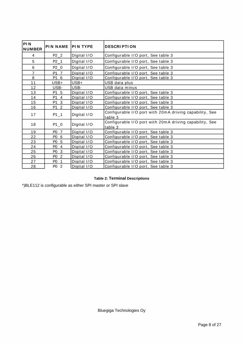
PIN NUMBER
PIN NAME PIN TYPE DESCRIPTION
4 P2_2 Digital I/O Configurable I/O port, See table 3
5 P2_1 Digital I/O Configurable I/O port, See table 3
6 P2_0 Digital I/O Configurable I/O port, See table 37 P1 7 Digital I/O Configurable I/O port, See table 38 P1_6 Digital I/O Configurable I/O port, See table 311 USB+ USB+ USB data plus12 USB- USB- USB data minus13 P1_5 Digital I/O Configurable I/O port, See table 314 P1_4 Digital I/O Configurable I/O port, See table 315 P1_3 Digital I/O Configurable I/O port, See table 316 P1_2 Digital I/O Configurable I/O port, See table 3
17 P1_1 Digital I/O Configurable I/O port with 20mA driving capability, See table 3
18 P1_0 Digital I/O Configurable I/O port with 20mA driving capability, See table 3
19 P0_7 Digital I/O Configurable I/O port, See table 322 P0_6 Digital I/O Configurable I/O port, See table 323 P0_5 Digital I/O Configurable I/O port, See table 324 P0_4 Digital I/O Configurable I/O port, See table 325 P0_3 Digital I/O Configurable I/O port, See table 326 P0_2 Digital I/O Configurable I/O port, See table 327 P0_1 Digital I/O Configurable I/O port, See table 328 P0_2 Digital I/O Configurable I/O port, See table 3
Table 2: Terminal Descriptions
*)BLE112 is configurable as either SPI master or SPI slave
Bluegiga Technologies Oy
Page 9 of 27
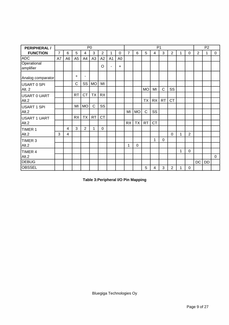
7 6 5 4 3 2 1 0 7 6 5 4 3 2 1 0 2 1 0ADC A7 A6 A5 A4 A3 A2 A1 A0Operational amplifier O - +
Analog comparator + -
C SS MO MI
MO MI C SS
RT CT TX RX
TX RX RT CT
MI MO C SS
MI MO C SS
RX TX RT CT
RX TX RT CT
4 3 2 1 0
3 4 0 1 2
1 0
1 0
1 0
0DEBUG DC DDOBSSEL 5 4 3 2 1 0
TIMER 1Alt.2
TIMER 3Alt.2
TIMER 4Alt.2
PERIPHERAL / FUNCTION
P0 P1 P2
USART 0 SPIAlt. 2
USART 0 UARTAlt.2
USART 1 SPIAlt.2
USART 1 UARTAlt.2
Table 3:Peripheral I/O Pin Mapping
Bluegiga Technologies Oy
Page 10 of 27
3 Electrical Characteristics
3.1 Absolute Maximum Ratings
Note: These are absolute maximum ratings beyond which the module can be permanently damaged. These are not maximum operating conditions. The maximum recommended operating conditions are in the table 5.
Min Max Unit-40 85 °C
-0.3 3.9 V
VSS-0.4 VDD+0.4 V
RatingStorage Temperature
Other Terminal Voltages
AVDD,DVDD, VDD_USB
Table 4: Absolute Maximum Ratings
3.2 Recommended Operating Conditions
Min Max Unit-40 85 °C2.0 3.6 V
RatingOperating Temperature RangeAVDD, DVDD, VDD_USB (*
*) Supply voltage noise should be less than 10mVpp. Excessive noise at the supply voltage will reduce the RF performance.
Table 5: Recommended Operating Conditions
For the I/O terminal characteristic refer to the CC2540 datasheet available in (http://www.ti.com/lit/ds/symlink/cc2540.pdf)
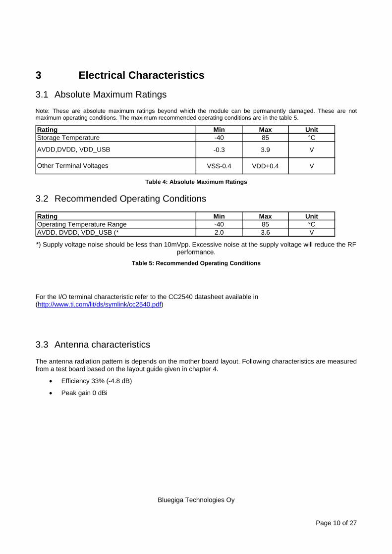
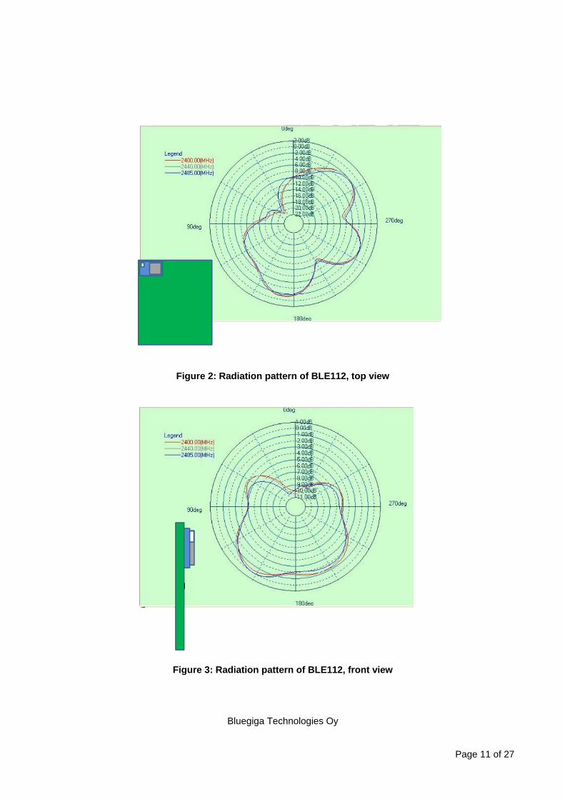
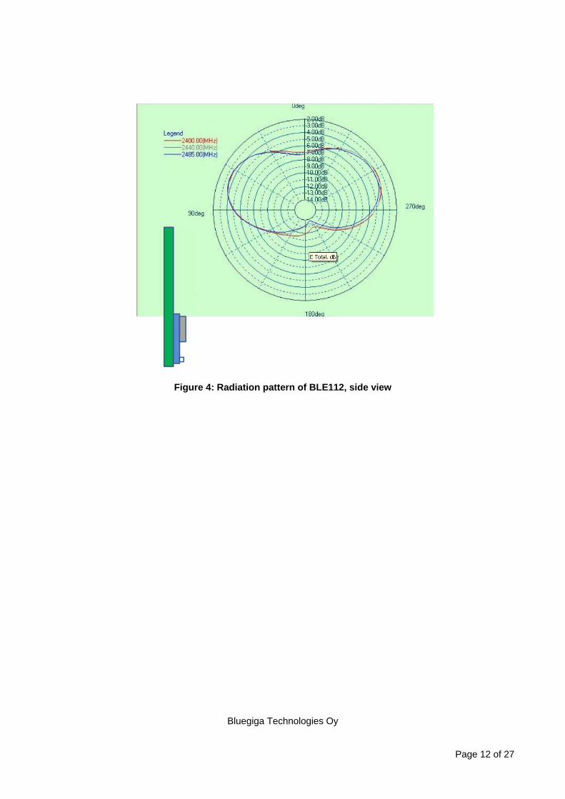
3.3 Antenna characteristics
The antenna radiation pattern is depends on the mother board layout. Following characteristics are measured from a test board based on the layout guide given in chapter 4.
Efficiency 33% (-4.8 dB)
Peak gain 0 dBi
Bluegiga Technologies Oy
Page 11 of 27
Figure 2: Radiation pattern of BLE112, top view
Figure 3: Radiation pattern of BLE112, front view
Bluegiga Technologies Oy
Page 12 of 27
Figure 4: Radiation pattern of BLE112, side view
Bluegiga Technologies Oy
Page 13 of 27
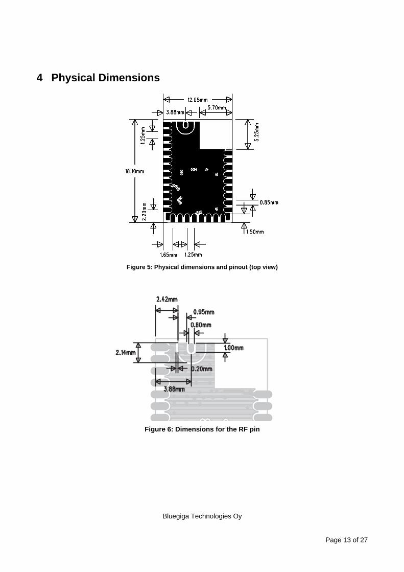
4 Physical Dimensions
Figure 5: Physical dimensions and pinout (top view)
Figure 6: Dimensions for the RF pin
Bluegiga Technologies Oy
Page 14 of 27
18.10 mm
12.0
5 m
m
Ant
enna
U.fl
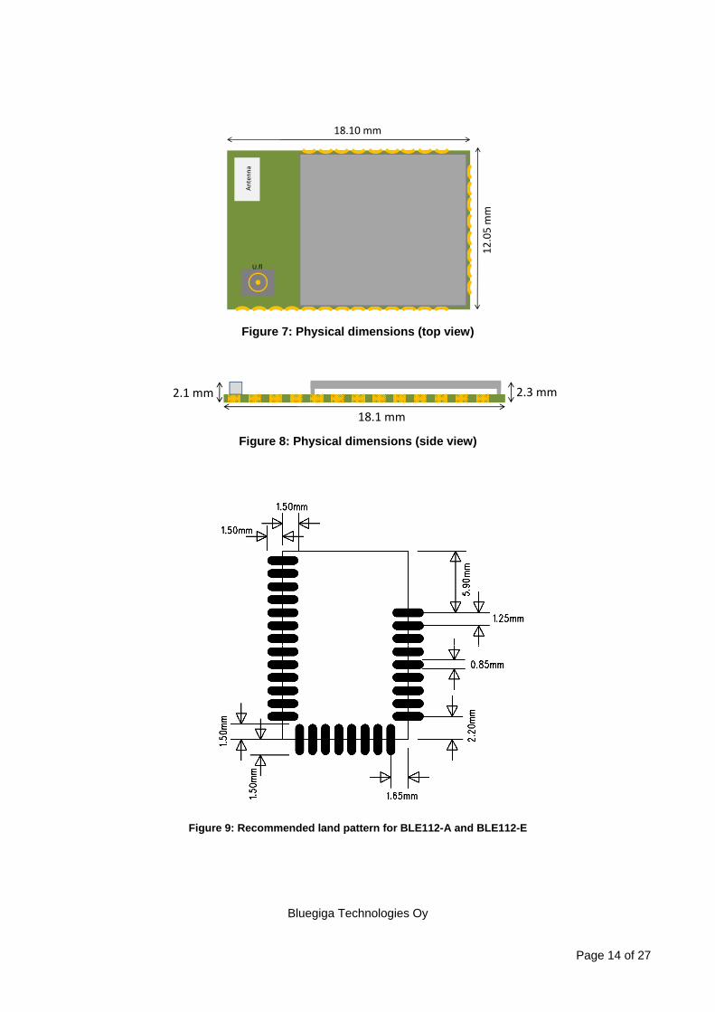
Figure 7: Physical dimensions (top view)
18.1 mm
2.1 mm 2.3 mm
Figure 8: Physical dimensions (side view)
Figure 9: Recommended land pattern for BLE112-A and BLE112-E
Bluegiga Technologies Oy
Page 15 of 27
5 Design Guidelines
5.1 General Design Guidelines
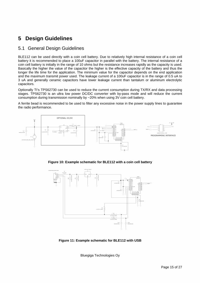
BLE112 can be used directly with a coin cell battery. Due to relatively high internal resistance of a coin cell battery it is recommended to place a 100uF capacitor in parallel with the battery. The internal resistance of a coin cell battery is initially in the range of 10 ohms but the resistance increases rapidly as the capacity is used. Basically the higher the value of the capacitor the higher is the effective capacity of the battery and thus the longer the life time for the application. The minimum value for the capacitor depends on the end application and the maximum transmit power used. The leakage current of a 100uF capacitor is in the range of 0.5 uA to 3 uA and generally ceramic capacitors have lower leakage current than tantalum or aluminum electrolytic capacitors.
Optionally TI’s TPS62730 can be used to reduce the current consumption during TX/RX and data processing stages. TPS62730 is an ultra low power DC/DC converter with by-pass mode and will reduce the current consumption during transmission nominally by ~20% when using 3V coin cell battery.
A ferrite bead is recommended to be used to filter any excessive noise in the power supply lines to guarantee the radio performance.
OPTIONAL DC/DC
PROGRAMMING INTERFACE1
2
U4
BATTERYHOLDER_SMD_CR2032
C15
100uF/6.3V/X5R
1STAT
2SW
3VIN
4G
ND5
ON/BYP
6VOUT
U5
TPS62730
C10
2.2uF/10V/X5R
C11
2.2uF/10V/X5R
L1
2.2μH±20%, 130mA, 0.43ohm 1GND
2AVDD
3AVDD
4P2_2
5P2_1
6P2_0
7P1_7
8P1_6
9DVDD_USB
10GND
11USB+
12USB-
13P1_5
14P
1_4
15P
1_3
16P
1_2
17P
1_1
18P
1_0
19P
0:7
20D
VD
D21
GN
D
22P0_6
23P0_5
24P0_4
25P0_3
26P0_2
27P0_1
28P0_0
29RESET
30GND
MOD2
BLE112-A1
3
5
2
4
6
7 8
9 10
J1
HEADER_2X5_SMD_1.27MM
C3
1uF/16V/X5R
C5
1uF/16V/X5R
C6
1uF/16V/X5R
P1_7/DCDC
VBAT
P2_2
2V...3V3_SW
P2_1
RESET_NRESET_N
P2_2P2_1
P1_7/DCDC
Figure 10: Example schematic for BLE112 with a coin cell battery
1VBUS
2D-
3D+
4NC
5GND
78 69
J10
CON-MINIUSB-SOCKET-SMD
C20
0.4
7uF/
6.3
V/X
5R
C31
2.2
uF/
10V/X
5R
C32
2.2
uF/
10V/X
5R
3VIN
2VOUT
1G
ND
P1
MCP1700T-3302E/T
L4
FB 1kohm
1 2R13
33R, 50V, 0.063W
1 2R14
33R, 50V, 0.063W
12
R15
1.5K, 50V, 0.063W
C127
47pF/50V/C0G
C128
47pF/50V/C0G
1GND
2AVDD
3AVDD
4P2_2
5P2_1
6P2_0
7P1_7
8P1_6
9DVDD_USB
10GND
11USB+
12USB-
13P1_5
14
P1
_4
15
P1
_3
16
P1
_2
17
P1
_1
18
P1
_0
19
P0
:72
0D
VD
D2
1G
ND
22P0_6
23P0_5
24P0_4
25P0_3
26P0_2
27P0_1
28P0_0
29RESET
30GND
MOD3
BLE112-A
C7
1uF/16V/X5R
C8
1uF/16V/X5R
C9
1uF/16V/X5R
RESET
Figure 11: Example schematic for BLE112 with USB
Bluegiga Technologies Oy
Page 16 of 27
5.2 Layout Guide Lines
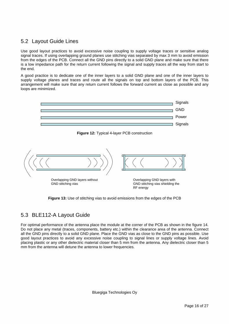
Use good layout practices to avoid excessive noise coupling to supply voltage traces or sensitive analog signal traces. If using overlapping ground planes use stitching vias separated by max 3 mm to avoid emission from the edges of the PCB. Connect all the GND pins directly to a solid GND plane and make sure that there is a low impedance path for the return current following the signal and supply traces all the way from start to the end.
A good practice is to dedicate one of the inner layers to a solid GND plane and one of the inner layers to supply voltage planes and traces and route all the signals on top and bottom layers of the PCB. This arrangement will make sure that any return current follows the forward current as close as possible and any loops are minimized.
Signals
GND
Power
Signals
Figure 12: Typical 4-layer PCB construction
Overlapping GND layers without GND stitching vias
Overlapping GND layers with GND stitching vias shielding the RF energy
Figure 13: Use of stitching vias to avoid emissions from the edges of the PCB
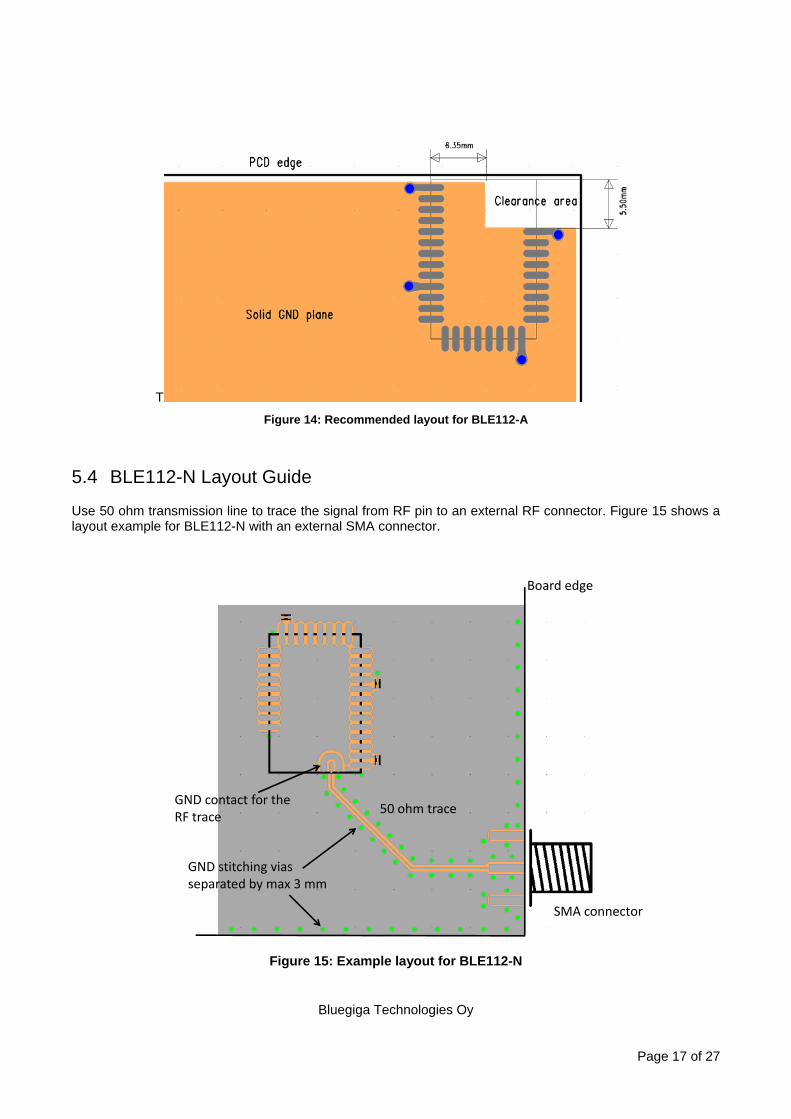
5.3 BLE112-A Layout Guide
For optimal performance of the antenna place the module at the corner of the PCB as shown in the figure 14. Do not place any metal (traces, components, battery etc.) within the clearance area of the antenna. Connect all the GND pins directly to a solid GND plane. Place the GND vias as close to the GND pins as possible. Use good layout practices to avoid any excessive noise coupling to signal lines or supply voltage lines. Avoid placing plastic or any other dielectric material closer than 5 mm from the antenna. Any dielectric closer than 5 mm from the antenna will detune the antenna to lower frequencies.
Bluegiga Technologies Oy
Page 17 of 27
T
Figure 14: Recommended layout for BLE112-A
5.4 BLE112-N Layout Guide
Use 50 ohm transmission line to trace the signal from RF pin to an external RF connector. Figure 15 shows a layout example for BLE112-N with an external SMA connector.
Board edge
SMA connector
50 ohm traceGND contact for the RF trace
GND stitching vias separated by max 3 mm
Figure 15: Example layout for BLE112-N
Bluegiga Technologies Oy
Page 18 of 27
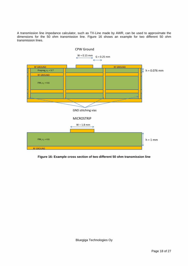
A transmission line impedance calculator, such as TX-Line made by AWR, can be used to approximate the dimensions for the 50 ohm transmission line. Figure 16 shows an example for two different 50 ohm transmission lines.
FR4, εr = 4.6
Prepreg, εr = 3.7
W = 0.15 mm
h = 0.076 mm
G = 0.25 mm
GND stitching vias
RF GROUND
RF GROUND RF GROUND
RF GROUND
FR4, εr = 4.6 h = 1 mm
W = 1.8 mm
MICROSTRIP
CPW Ground
Figure 16: Example cross section of two different 50 ohm transmission line

Bluegiga Technologies Oy
Page 19 of 27
6 Soldering Recommendations
BLE112 is compatible with industrial standard reflow profile for Pb-free solders. The reflow profile used is dependent on the thermal mass of the entire populated PCB, heat transfer efficiency of the oven and particular type of solder paste used. Consult the datasheet of particular solder paste for profile configurations.
Bluegiga Technologies will give following recommendations for soldering the module to ensure reliable solder joint and operation of the module after soldering. Since the profile used is process and layout dependent, the optimum profile should be studied case by case. Thus following recommendation should be taken as a starting point guide.
- Refer to technical documentations of particular solder paste for profile configurations
- Avoid using more than one flow.
- Reliability of the solder joint and self-alignment of the component are dependent on the solder volume. Minimum of 150m stencil thickness is recommended.
- Aperture size of the stencil should be 1:1 with the pad size.
- A low residue, “no clean” solder paste should be used due to low mounted height of the component.
Bluegiga Technologies Oy
Page 20 of 27
7 Block diagram
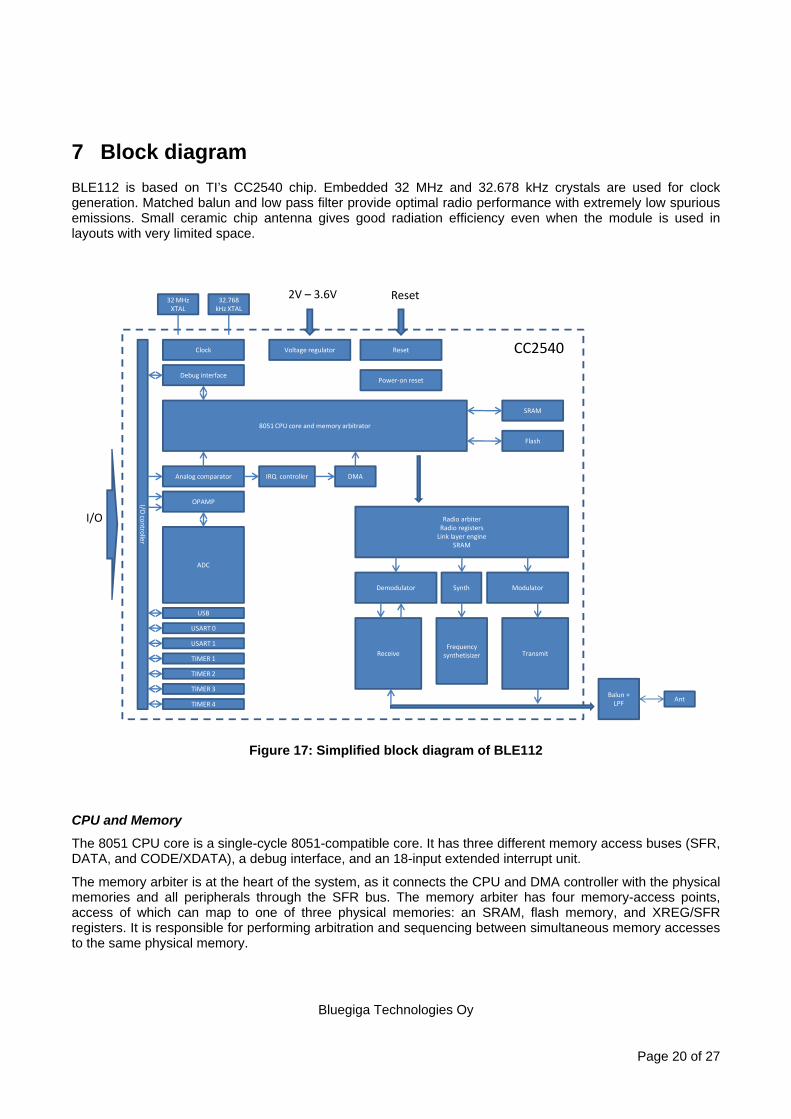
BLE112 is based on TI’s CC2540 chip. Embedded 32 MHz and 32.678 kHz crystals are used for clock generation. Matched balun and low pass filter provide optimal radio performance with extremely low spurious emissions. Small ceramic chip antenna gives good radiation efficiency even when the module is used in layouts with very limited space.
I/O controller
CC2540
I/O
32 MHz XTAL
32.768 kHz XTAL
Clock
Debug interface
8051 CPU core and memory arbitrator
Voltage regulator
SRAM
Flash
Analog comparator
OPAMP
ADC
IRQ controller DMA
USB
USART 0
USART 1
TIMER 1
TIMER 2
TIMER 3
TIMER 4
Radio arbiterRadio registers
Link layer engineSRAM
ModulatorDemodulator Synth
Receive TransmitFrequency
synthetisizer
Balun + LPF
Ant
Reset
Power-on reset
2V – 3.6V Reset
Figure 17: Simplified block diagram of BLE112
CPU and Memory
The 8051 CPU core is a single-cycle 8051-compatible core. It has three different memory access buses (SFR, DATA, and CODE/XDATA), a debug interface, and an 18-input extended interrupt unit.
The memory arbiter is at the heart of the system, as it connects the CPU and DMA controller with the physical memories and all peripherals through the SFR bus. The memory arbiter has four memory-access points, access of which can map to one of three physical memories: an SRAM, flash memory, and XREG/SFR registers. It is responsible for performing arbitration and sequencing between simultaneous memory accesses to the same physical memory.

Bluegiga Technologies Oy
Page 21 of 27
The SFR bus is a common bus that connects all hardware peripherals to the memory arbiter. The SFR bus also provides access to the radio registers in the radio register bank, even though these are indeed mapped into XDATA memory space.
The 8-KB SRAM maps to the DATA memory space and to parts of the XDATA memory spaces. The SRAM is an ultralow-power SRAM that retains its contents even when the digital part is powered off (power modes 2 and 3).
The 128/256 KB flash block provides in-circuit programmable non-volatile program memory for the device, and maps into the CODE and XDATA memory spaces.
Peripherals
Writing to the flash block is performed through a flash controller that allows page-wise erasure and 4-bytewise programming.
A versatile five-channel DMA controller is available in the system, accesses memory using the XDATA memory space, and thus has access to all physical memories. Each channel (trigger, priority, transfer mode, addressing mode, source and destination pointers, and transfer count) is configured with DMA descriptors that can be located anywhere in memory. Many of the hardware peripherals (AES core, flash controller, USARTs, timers, ADC interface, etc.) can be used with the DMA controller for efficient operation by performing data transfers between a single SFR or XREG address and flash/SRAM.
Each CC2540 contains a unique 48-bit IEEE address that can be used as the public device address for a Bluetooth device. Designers are free to use this address, or provide their own, as described in the Bluetooth specification.
The interrupt controller services a total of 18 interrupt sources, divided into six interrupt groups, each of which is associated with one of four interrupt priorities. I/O and sleep timer interrupt requests are serviced even if the device is in a sleep mode (power modes 1 and 2) by bringing the CC2540 back to the active mode.
The debug interface implements a proprietary two-wire serial interface that is used for in-circuit debugging. Through this debug interface, it is possible to erase or program the entire flash memory, control which oscillators are enabled, stop and start execution of the user program, execute instructions on the 8051 core, set code breakpoints, and single-step through instructions in the code. Using these techniques, it is possible to perform in-circuit debugging and external flash programming elegantly.
The I/O controller is responsible for all general-purpose I/O pins. The CPU can configure whether peripheral modules control certain pins or whether they are under software control, and if so, whether each pin is configured as an input or output and if a pullup or pulldown resistor in the pad is connected. Each peripheral that connects to the I/O pins can choose between two different I/O pin locations to ensure flexibility in various applications.
The sleep timer is an ultra low power timer that uses an external 32.768-kHz crystal oscillator. The sleep timer runs continuously in all operating modes except power mode 3. Typical applications of this timer are as a real-time counter or as a wake-up timer to exit power modes 1 or 2.
A built-in watchdog timer allows the CC2540 to reset itself if the firmware hangs. When enabled by software, the watchdog timer must be cleared periodically; otherwise, it resets the device when it times out.
Timer 1 is a 16-bit timer with timer/counter/PWM functionality. It has a programmable prescaler, a 16-bit period value, and five individually programmable counter/capture channels, each with a 16-bit compare value. Each of the counter/capture channels can be used as a PWM output or to capture the timing of edges on input signals. It can also be configured in IR generation mode, where it counts timer 3 periods and the output is ANDed with the output of timer 3 to generate modulated consumer IR signals with minimal CPU interaction.
Timer 2 is a 40-bit timer used by the Bluetooth low energy stack. It has a 16-bit counter with a configurable timer period and a 24-bit overflow counter that can be used to keep track of the number of periods that have transpired. A 40-bit capture register is also used to record the exact time at which a start-of-frame delimiter is received/transmitted or the exact time at which transmission ends. There are two 16-bit timer-compare registers and two 24-bit overflow-compare registers that can be used to give exact timing for start of RX or TX to the radio or general interrupts.

Bluegiga Technologies Oy
Page 22 of 27
Timer 3 and timer 4 are 8-bit timers with timer/counter/PWM functionality. They have a programmable prescaler, an 8-bit period value, and one programmable counter channel with an 8-bit compare value. Each of the counter channels can be used as PWM output.
USART 0 and USART 1 are each configurable as either an SPI master/slave or a UART. They provide double buffering on both RX and TX and hardware flow control and are thus well suited to high-throughput full-duplex applications. Each USART has its own high-precision baud-rate generator, thus leaving the ordinary timers free for other uses. When configured as SPI slaves, the USARTs sample the input signal using SCK directly instead of using some oversampling scheme, and are thus well-suited for high data rates.
The AES encryption/decryption core allows the user to encrypt and decrypt data using the AES algorithm with 128-bit keys. The AES core also supports ECB, CBC, CFB, OFB, CTR, and CBC-MAC, as well as hardware support for CCM.
The ADC supports 7 to 12 bits of resolution with a corresponding range of bandwidths from 30-kHz to 4-kHz, respectively. DC and audio conversions with up to eight input channels (I/O controller pins) are possible. The inputs can be selected as single-ended or differential. The reference voltage can be internal, AVDD, or a single-ended or differential external signal. The ADC also has a temperature-sensor input channel. The ADC can automate the process of periodic sampling or conversion over a sequence of channels.
The operational amplifier is intended to provide front-end buffering and gain for the ADC. Both inputs as well as the output are available on pins, so the feedback network is fully customizable. A chopper-stabilized mode is available for applications that need good accuracy with high gain.
The ultralow-power analog comparator enables applications to wake up from PM2 or PM3 based on an analog signal. Both inputs are brought out to pins; the reference voltage must be provided externally. The comparator output is connected to the I/O controller interrupt detector and can be treated by the MCU as a regular I/O pin interrupt.
RF front end
RF front end includes combined matched balun and low pass filter, and ceramic chip antenna with matching network. Optimal matching combined with effective low pass filter provides extremely low in-band spurious emissions and harmonics. Optionally as a module assembly variant RF can be traced either to an embedded u.fl connector or to the RF pin of the module.
Bluegiga Technologies Oy
Page 23 of 27
8 Certifications
BLE112 is compliant to the following specifications.
8.1 Bluetooth
BLE112 Bluetooth low energy module is Bluetooth qualified and listed as a controller subsystem and it is Bluetooth compliant to the following profiles of the core spec version v.4.0:
RF PHY
HCI
LL
The maximum antenna gain specified for BLE112 is 2.3 dBi. Bluetooth qualification is valid for any antenna with gain less than 2.3 dBi.
8.2 FCC and IC
This device complies with Part 15 of the FCC Rules. Operation is subject to the following two conditions:
(1) this device may not cause harmful interference, and
(2) this device must accept any interference received, including interference that may cause undesired operation.
FCC RF Radiation Exposure Statement:
This equipment complies with FCC radiation exposure limits set forth for an uncontrolled environment. End users must follow the specific operating instructions for satisfying RF exposure compliance. This transmitter must not be co-located or operating in conjunction with any other antenna or transmitter.
IC Statements:
This device complies with Industry Canada licence-exempt RSS standard(s). Operation is subject to the following two conditions: (1) this device may not cause interference, and (2) this device must accept any interference, including interference that may cause undesired operation of the device.
Under Industry Canada regulations, this radio transmitter may only operate using an antenna of a type and maximum (or lesser) gain approved for the transmitter by Industry Canada. To reduce potential radio interference to other users, the antenna type and its gain should be so chosen that the equivalent isotropically radiated power (e.i.r.p.) is not more than that necessary for successful communication.
If detachable antennas are used:

Bluegiga Technologies Oy
Page 24 of 27
This radio transmitter (identify the device by certification number, or model number ifCategory II) has been approved by Industry Canada to operate with the antenna types listed below with the maximum permissible gain and required antenna impedance for each antenna type indicated. Antenna types not included in this list, having a gain greater than the maximum gain indicated for that type, are strictly prohibited for use with this device. See table 7 for the approved antennas for BLE112.
OEM Responsibilities to comply with FCC and Industry Canada Regulations
The BLE112 module has been certified for integration into products only by OEM integrators under the following condition:
The transmitter module must not be co-located or operating in conjunction with any other antenna or transmitter.
As long as the condition above is met, further transmitter testing will not be required. However, the OEM integrator is still responsible for testing their end-product for any additional compliance requirements required with this module installed (for example, digital device emissions, PC peripheral requirements, etc.).
IMPORTANT NOTE: In the event that these conditions can not be met (for certain configurations or co-location with another transmitter), then the FCC and Industry Canada authorizations are no longer considered valid and the FCC ID and IC Certification Number can not be used on the final product. In these circumstances, the OEM integrator will be responsible for re-evaluating the end product (including the transmitter) and obtaining a separate FCC and Industry Canada authorization.
End Product Labeling
The BLE112 module is labeled with its own FCC ID and IC Certification Number. If the FCC ID and IC Certification Number are not visible when the module is installed inside another device, then the outside of the device into which the module is installed must also display a label referring to the enclosed module. In that case, the final end product must be labeled in a visible area with the following:
“Contains Transmitter Module FCC ID: QOQBLE112”
“Contains Transmitter Module IC: 5123A-BGTBLE112”
or
“Contains FCC ID: QOQBLE112
“Contains IC: 5123A-BGTBLE112”
The OEM of the BLE112 module must only use the approved antenna(s) listed in table 7, which have been certified with this module.
The OEM integrator has to be aware not to provide information to the end user regarding how to install or remove this RF module or change RF related parameters in the user manual of the end product.
Déclaration d’IC :
Ce dispositif est conforme aux normes RSS exemptes de licence d’Industrie Canada. Son fonctionnement est assujetti aux deux conditions suivantes : (1) ce dispositif ne doit pas provoquer de perturbation et (2) ce
Bluegiga Technologies Oy
Page 25 of 27
dispositif doit accepter toute perturbation, y compris les perturbations qui peuvent entraîner un fonctionnement non désiré du dispositif.
Selon les réglementations d’Industrie Canada, cet émetteur radio ne doit fonctionner qu’avec une antenne d’une typologie spécifique et d’un gain maximum (ou inférieur) approuvé pour l’émetteur par Industrie Canada. Pour réduire les éventuelles perturbations radioélectriques nuisibles à d’autres utilisateurs, le type d’antenne et son gain doivent être choisis de manière à ce que la puissance isotrope rayonnée équivalente (P.I.R.E.) n’excède pas les valeurs nécessaires pour obtenir une communication convenable.
Si des antennes amovibles sont utilisées :
Cet émetteur radio (identifier le dispositif à l’aide de son numéro de certification ou de son numéro de modèle s’il appartient à la Catégorie II) a été approuvé par Industrie Canada pour fonctionner avec les types d’antenne énumérés ci-dessous, avec le gain admissible maximum et l’impédance d’antenne requise pour chaque type d’antenne indiqué. Les types d’antennes qui ne figurent pas dans cette liste ont un gain supérieur au gain maximum indiqué pour ce type ; il est donc strictement défendu de les utiliser avec ce dispositif. Consulter le tableau 7 pour découvrir les antennes approuvées pour BLE112.
Responsabilités des OEM quant à la conformité avec les réglementations de FCC et d’Industrie Canada
Le module BLE112 a été certifié pour être intégré à des produits fabriqués uniquement par les intégrateurs OEM dans les conditions suivantes :Le module de l’émetteur ne doit pas être situé près d’une autre antenne
ou d’un autre émetteur ni ou fonctionner conjointement avec ceux-ci.
Dans la mesure où cette condition est observée, il ne sera pas nécessaire de soumettre l’émetteur à des essais supplémentaires. Cependant, l’intégrateur OEM est chargé de tester son produit final pour s’assurer qu’il respecte toutes les autres exigences de conformité requises avec ce module installé (par exemple : émissions du dispositif numérique, exigences périphériques de l’ordinateur, etc.).
REMARQUE IMPORTANTE : En cas d’inobservance de ces conditions (en ce qui concerne certaines configurations ou l’emplacement du dispositif à proximité d’un autre émetteur), les autorisations de FCC et d’Industrie Canada ne seront plus considérées valables et l’identification de FCC et le numéro de certification d’IC ne pourront pas être utilisés sur le produit final. Dans ces cas, l’intégrateur OEM sera chargé d’évaluer à nouveau le produit final (y compris l’émetteur) et d’obtenir une autorisation indépendante de FCC et d’Industrie Canada.
Étiquetage du produit final
Le module BLE112 est étiqueté avec sa propre identification FCC et son propre numéro de certification IC. Si l’identification FCC et le numéro de certification IC ne sont pas visibles lorsque le module est installé à l’intérieur d’un autre dispositif, la partie externe du dispositif dans lequel le module est installé devra également présenter une étiquette faisant référence au module inclus. Dans ce cas, le produit final devra être étiqueté sur une zone visible avec les informations suivantes :
« Contient module émetteur identification FCC : QOQBLE112 »
« Contient module émetteur IC : 5123A-BGTBLE112 »
ou
« Contient identification FCC : QOQBLE112 »
« Contient IC : 5123A-BGTBLE112 »
Bluegiga Technologies Oy
Page 26 of 27
L’OEM du module BLE112 ne doit utiliser que la ou les antennes approuvées énumérées dans le tableau 7, qui ont été certifiées avec ce module.
Dans le guide d’utilisation du produit final, l’intégrateur OEM doit s’abstenir de fournir des informations à l’utilisateur final portant sur les procédures à suivre pour installer ou retirer ce module RF ou pour changer les paramètres RF.
8.3 CE
BLE112 is in conformity with the essential requirements and other relevant requirements of the R&TTE Directive (1999/5/EC). The product is conformity with the following standards and/or normative documents.
EMC (immunity only) EN 301 489-17 V.1.3.3 in accordance with EN 301 489-1 V1.8.1
Radiated emissions EN 300 328 V1.7.1
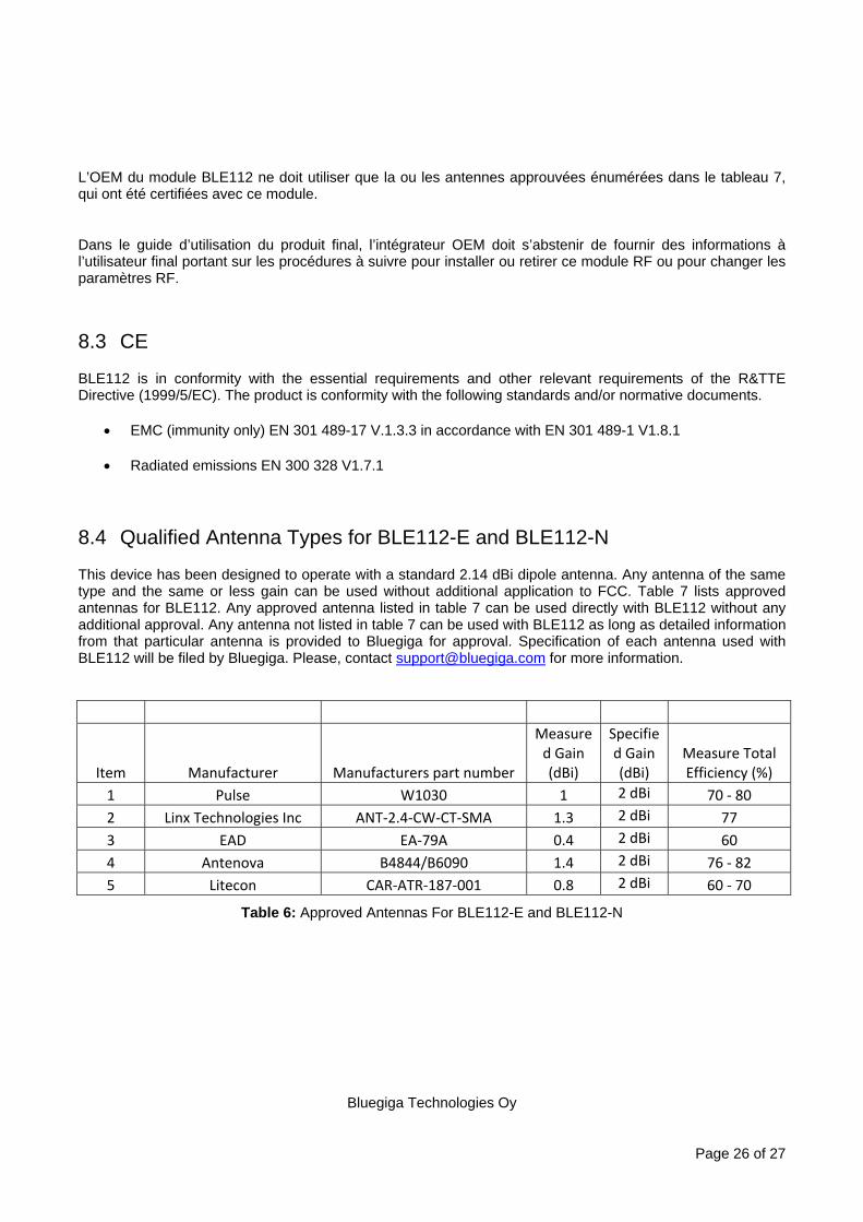
8.4 Qualified Antenna Types for BLE112-E and BLE112-N
This device has been designed to operate with a standard 2.14 dBi dipole antenna. Any antenna of the same type and the same or less gain can be used without additional application to FCC. Table 7 lists approved antennas for BLE112. Any approved antenna listed in table 7 can be used directly with BLE112 without any additional approval. Any antenna not listed in table 7 can be used with BLE112 as long as detailed information from that particular antenna is provided to Bluegiga for approval. Specification of each antenna used with BLE112 will be filed by Bluegiga. Please, contact [email protected] for more information.
Item Manufacturer Manufacturers part number
Measured Gain (dBi)
Specified Gain (dBi)
Measure Total Efficiency (%)
1 Pulse W1030 1 2 dBi 70 - 80 2 Linx Technologies Inc ANT-2.4-CW-CT-SMA 1.3 2 dBi 77 3 EAD EA-79A 0.4 2 dBi 60 4 Antenova B4844/B6090 1.4 2 dBi 76 - 82 5 Litecon CAR-ATR-187-001 0.8 2 dBi 60 - 70
Table 6: Approved Antennas For BLE112-E and BLE112-N
Bluegiga Technologies Oy
Page 27 of 27
9 Contact Information
Sales: [email protected]
Technical support: [email protected]
http://techforum.bluegiga.com
Orders: [email protected]
WWW: www.bluegiga.com
www.bluegiga.hk
Head Office / Finland:
Phone: +358-9-4355 060
Fax: +358-9-4355 0660
Sinikalliontie 5A
02630 ESPOO
FINLAND
Postal address / Finland:
P.O. BOX 120
02631 ESPOO
FINLAND
Sales Office / USA:
Phone: +1 770 291 2181
Fax: +1 770 291 2183
Bluegiga Technologies, Inc.
3235 Satellite Boulevard, Building 400, Suite 300
Duluth, GA, 30096, USA
Sales Office / Hong-Kong:
Phone: +852 3182 7321
Fax: +852 3972 5777
Bluegiga Technologies, Inc.
19/F Silver Fortune Plaza, 1 Wellington Street,
Central Hong Kong