Active Piezoelectric Diaphragms - Old Dominion …mln/ltrs-pdfs/NASA-2002-9spiessm-rgb.pdf2.2....
12
Active Piezoelectric Diaphragms Robert G. Bryant 1 , Robert T. Effinger IV 2 , Isaiah Aranda Jr. 3 , Ben M. Copeland Jr. 4 and Ed W. Covington III 5 NASA Langley Research Center, MS 226 1 , MS 390 4 , MS 384 5 , Hampton, VA 23681 2 USRP Student, Texas A&M, Dept of Mech. Eng., College Station, TX 77840 3 LARSS Student, Texas A&M, Dept. of Mech. Eng., Kingsville TX.78363 ACTIVE MATERIALS: BEHAVIOR AND MECHANICS ABSTRACT Several active piezoelectric diaphragms were fabricated by placing unelectroded piezoelectric disks between copper clad films patterned with I nter-C irculating E lectrodes "ICE". When a voltage potential is applied to the electrodes, the result is radially distributed electric field that mechanically strains the piezo-ceramic along the Z-axis (perpendicular to the applied electric field), rather than the expected in-plane (XY-axis) direction. Unlike other out of plane piezoelectric actuators, which are benders, these R adial F ield D iaphragms (RFDs) strain concentrically yet afford high displacements while maintaining a constant circumference. This paper covers the fabrication and characterization of these diaphragms as a function of poling field strength, ceramic diameter and line spacing, as well as the surface topography, the resulting strain field and displacement as a function of applied voltage ranging from DC to 10 Hz. Keywords : Piezoelectric actuators, Piezoelectric diaphragms, Active materials, Radial Field Diaphragms, NASA RFDs 1. INTRODUCTION The design and performance of NASA LaRC’s Radial Field Diaphragm piezoelectric actuator with Inter- Circulating Electrodes “ICE-RFD” is presented. The RFD is comprised of a thin circular piezoelectric ceramic disk sandwiched between two polyimide “PI” dielectric films with copper-etched spiral electrodes. On each spiraled electrode pattern, positive and negative electrodes spiral inward to the center of the disk in a serpentine manner. This novel electrode pattern induces an electric field into the piezo-ceramic that extends out radially from the center of the wafer. The dielectric film serves as the electrode carrier and insulator. The RFD design is shown in Figure 1. Electric Field Copper Electrodes PI Dielectric film RFD With ICE Electric Field Vector Displacement Piezoceramic Cross Sectional View Figure 1 : Cartoon showing RFD & inter-circulated electrodes. The NASA LaRC RFD actuator design has several distinct differences from conventional piezoelectric actuators, and its LaRC predecessors: the NASA Thunder and NASA MFC, when fixed about their perimeter [1-4]. Because of its radial design, the ICE-RFD exhibits out of plane movement, when electrically stimulated, and does not transmit any substantial mechanical strain beyond the boundary of the ceramic element. This behavior is distinct from all other “bender” type actuators. Proceedings of SPIE, Smart Structures and Materials – Active Materials : Behavior and Mechanics, Paper 4699-40, San Diego, CA (2002). 1
Transcript of Active Piezoelectric Diaphragms - Old Dominion …mln/ltrs-pdfs/NASA-2002-9spiessm-rgb.pdf2.2....

Active Piezoelectric Diaphragms
Robert G. Bryant1, Robert T. Effinger IV2, Isaiah Aranda Jr.3, Ben M. Copeland Jr.4 and Ed W. Covington III5
NASA Langley Research Center, MS 2261, MS 3904, MS 3845, Hampton, VA 23681 2USRP Student, Texas A&M, Dept of Mech. Eng., College Station, TX 77840
3LARSS Student, Texas A&M, Dept. of Mech. Eng., Kingsville TX.78363
ACTIVE MATERIALS: BEHAVIOR AND MECHANICS
ABSTRACT Several active piezoelectric diaphragms were fabricated by placing unelectroded piezoelectric disks between copper clad films patterned with Inter-Circulating Electrodes "ICE". When a voltage potential is applied to the electrodes, the result is radially distributed electric field that mechanically strains the piezo-ceramic along the Z-axis (perpendicular to the applied electric field), rather than the expected in-plane (XY-axis) direction. Unlike other out of plane piezoelectric actuators, which are benders, these Radial Field Diaphragms (RFDs) strain concentrically yet afford high displacements while maintaining a constant circumference. This paper covers the fabrication and characterization of these diaphragms as a function of poling field strength, ceramic diameter and line spacing, as well as the surface topography, the resulting strain field and displacement as a function of applied voltage ranging from DC to 10 Hz. Keywords: Piezoelectric actuators, Piezoelectric diaphragms, Active materials, Radial Field Diaphragms, NASA RFDs
1. INTRODUCTION
The design and performance of NASA LaRC’s Radial Field Diaphragm piezoelectric actuator with Inter-Circulating Electrodes “ICE-RFD” is presented. The RFD is comprised of a thin circular piezoelectric ceramic disk sandwiched between two polyimide “PI” dielectric films with copper-etched spiral electrodes. On each spiraled electrode pattern, positive and negative electrodes spiral inward to the center of the disk in a serpentine manner. This novel electrode pattern induces an electric field into the piezo-ceramic that extends out radially from the center of the wafer. The dielectric film serves as the electrode carrier and insulator. The RFD design is shown in Figure 1.
☺
Electric Field
Copper Electrodes
PI Dielectric film
RFD With ICE
Electric Field Vector
Displacement
Piezoceramic Cross Sectional View
Figure 1: Cartoon showing RFD & inter-circulated electrodes.
The NASA LaRC RFD actuator design has several distinct differences from conventional piezoelectric actuators, and its LaRC predecessors: the NASA Thunder and NASA MFC, when fixed about their perimeter [1-4]. Because of its radial design, the ICE-RFD exhibits out of plane movement, when electrically stimulated, and does not transmit any substantial mechanical strain beyond the boundary of the ceramic element. This behavior is distinct from all other “bender” type actuators.
Proceedings of SPIE, Smart Structures and Materials – Active Materials : Behavior and Mechanics, Paper 4699-40, San Diego, CA (2002). 1
Being the latest of the NASA LaRC smart material actuators, the RFD retains the advantageous laminate construction and fabrication techniques of its predecessor, the LaRC MFC actuator. The RFD possesses several new and unique characteristics including out-of-plane concentric actuation, unconstrained motion under fixed boundary conditions and the ability to use solid unelectroded ceramic plates.
Characterization of the ICE-RFD actuator is currently underway at NASA LaRC. Actuator design variables considered during the characterization tests include: the initial poling voltage, electrode pattern line thickness and spacing, ceramic disk thickness and diameter, and localized strain field data. The fabrication of the RFD actuators and the preliminary results of these test and their effect on low frequency displacement are discussed in this paper.
2. EXPERIMENTAL All materials used to make the RFD are commercially available and are listed in Table 1.
Table 1. NASA LaRC RFD Actuator Components and Manufacturers.
Material Manufacturer Website
Piezoceramic Wafer Morgan Matroc (PZT-5A) CTS (3195HD)
www.morganmatroc.com www.ctscorp.com
Adhesive Loctite Durabond E-120 HP Adhesive www.loctite.com
Copper Clad PI Film DuPont Pyralux LF8051 www.dupont.com
Release Film Pacothane Technologies www.pacothane.com
Press Pads Pacothane Technologies www.pacothane.com Metal-backed Piezo-diaphragm Murata Electronics Inc. #7BB-50-1A13 www.murata.com
2.1. RFD Piezoelectric Actuator Fabrication Procedures A.) Assembly
a) All the above materials (except the adhesive and Piezo-diaphragm) are wiped clean with ethanol using a lint-free cloth. After cleaning, the parts are handled with latex gloves to prevent contamination.
b) Apply the adhesive to the copper side of PI clad films (copper etched electrode patterns facing up) uniformly across both right and left spiral electrode patterns.
c) Doctor a thin coat of adhesive uniformly to one side of the ceramic wafer. Center the wafer on the right spiral electrode pattern and doctor a thin layer of adhesive to the exposed side of the ceramic wafer. Set the left spiral electrode clad facedown on the exposed ceramic.
d) Carefully center the top and bottom electrode patterns. Once in place, remove any air pockets by carefully applying pressure to the top electrode pattern, flip the piezo-laminate and continue to remove any trapped air.
B.) Curing Process:
a) Select aluminum plates and press pads larger than the actuator. Set the aluminum plate on a level surface and place two press pads on top of the plate followed by one sheet of release film. Place the piezo-laminate on this stack. Put another layer of release film on top of the actuator followed by two more press pads and another 1/8” aluminum plate.
b) Put the assembly into the vacuum press and apply vacuum for about 1 minute. Then close the clamps to remove any air pockets from between the wafer, epoxy, and electrode patterns. Reopen the clamp and hold vacuum for 10 minutes.
c) Heat the press to 125°C (250°F), close the clamps and apply 690 KPa (100 psi) for 2 hours. d) Cool the press until the system reaches 350C (95OF), then release clamp pressure and vacuum. e) Open clamps and remove the actuator.
Proceedings of SPIE, Smart Structures and Materials – Active Materials : Behavior and Mechanics, Paper 4699-40, San Diego, CA (2002). 2
2.2. Characterization
A.) The topographical profile data as a function of DC voltage was acquired using a Brown & Sharp Chameleon 153010 5S2 Validator; the low frequency displacement data was acquired with the use of a Newport 850F LVDT. In both cases a Trek Model 10/10B amplifier was the high voltage supply and the RFD actuators were mechanically constrained 2-3 mm (~3/32”) from the ceramic perimeter using PMMA circular window clamps.
B.) In-plain radial and tangential localized strain data were acquired with XY series C-891110-A and C-891113-C
wire-resistance strain gauges (Measurements Group, Inc.) and a Trek Model 609E-6 high voltage amplifier. All data (except the topographical profiles) was acquired on a PC using Lab-View data acquisition software running under Microsoft Windows. All RFD strain gauge measurements measured without any mechanical constraints.
2.3. Conversion Factors
1 mil = 25.4 (~25) µm. 1 mm = 39.37 (~40) mil. 1 inch = 2.54 cm.
3. RESULTS AND DISCUSSION 3.1. Fabrication
The manufacture of RFD actuators is accomplished in a multi-step process. This involves bonding two mirror imaged PI spiral electrode patterns to the ceramic wafer. The adhesive used determines the actual heating and bonding pressures, and in most cases, the temperature use range. It is important to remove any trapped air and inspect the wafer and electrode patterns prior to assembly as these defects can cause electrical shorts.
An actuator’s performance is highly dependent upon aspects of its design and fabrication. Common methods used to measure the performance of piezoelectric actuators include; strain per volt, strain as a function of frequency, life cycle performance, electro-mechanical efficiency, and environmental durability.
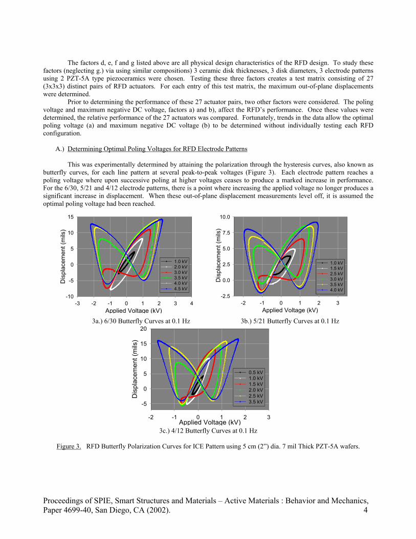
A convention has been adopted to help distinguish between the different electrode patterns presented. As shown in Figure 2, two numbers, separated by a “/”, will be used to describe the electrode patterns. The first number is the electrode line thickness and the second number is the center-to-center spacing between electrodes, all in mils as indicated. The initial research covers the first three, 6/30, 5/21 and 4/12, line patterns. The other necessary physical distinctions between RFD designs, namely, the ceramic disk thickness and disk diameter will be self-explanatory.
Figure 2. Numbering System for electrode patterns.
½
4/121
mils
— m
m---
010203040
½
5/211
010203040
mils
— m
m---
½
6/301
0 10 20 30 40
mils
— m
m---
3.2. Characterization Several RFD design parameters were varied to determine which ones affected the out-of-plane displacement of the RFD actuators. The factors tested were:
a.) initial poling voltage b.) actuator de-poling limit c.) operating frequency d.) electrode thickness and spacing e.) ceramic wafer thickness f.) ceramic wafer diameter g.) ceramic composition
Proceedings of SPIE, Smart Structures and Materials – Active Materials : Behavior and Mechanics, Paper 4699-40, San Diego, CA (2002). 3
The factors d, e, f and g listed above are all physical design characteristics of the RFD design. To study these factors (neglecting g.) via using similar compositions) 3 ceramic disk thicknesses, 3 disk diameters, 3 electrode patterns using 2 PZT-5A type piezoceramics were chosen. Testing these three factors creates a test matrix consisting of 27 (3x3x3) distinct pairs of RFD actuators. For each entry of this test matrix, the maximum out-of-plane displacements were determined.
Prior to determining the performance of these 27 actuator pairs, two other factors were considered. The poling voltage and maximum negative DC voltage, factors a) and b), affect the RFD’s performance. Once these values were determined, the relative performance of the 27 actuators was compared. Fortunately, trends in the data allow the optimal poling voltage (a) and maximum negative DC voltage (b) to be determined without individually testing each RFD configuration.
A.) Determining Optimal Poling Voltages for RFD Electrode Patterns
This was experimentally determined by attaining the polarization through the hysteresis curves, also known as butterfly curves, for each line pattern at several peak-to-peak voltages (Figure 3). Each electrode pattern reaches a poling voltage where upon successive poling at higher voltages ceases to produce a marked increase in performance. For the 6/30, 5/21 and 4/12 electrode patterns, there is a point where increasing the applied voltage no longer produces a significant increase in displacement. When these out-of-plane displacement measurements level off, it is assumed the optimal poling voltage had been reached.
Applied Voltage (kV)-2 -1 0 1 2 3
Dis
plac
emen
t (m
ils)
-2.5
0.0
2.5
5.0
7.5
10.0
1.0 kV1.5 kV2.5 kV3.0 kV3.5 kV4.0 kV
Applied Voltage (kV)-3 -2 -1 0 1 2 3 4
Dis
plac
emen
t (m
ils)
-10
-5
0
5
10
15
1.0 kV2.0 kV3.0 kV3.5 kV4.0 kV4.5 kV
3a.) 6/30 B rfly Curves at 0.1 Hz utterfly Curves at 0.1 Hz 3b.) 5/21 Butte
3c.) 4/12 Butterfly Curves at 0.1 Hz
Figure 3.
Applied Voltage (kV)-2 -1 0 1 2 3
Dis
plac
emen
t (m
ils)
-5
0
5
10
15
20
0.5 kV1.0 kV1.5 kV2.0 kV2.5 kV3.5 kV
RFD Butterfly Polarization 2”) dia. 7 mil Thick PZT-5A wafers. Curves for ICE Pattern using 5 cm (
Proceedings of SPIE, Smart Structures and Materials – Active Materials : Behavior and Mechanics, Paper 4699-40, San Diego, CA (2002). 4

These tests were done by first determining the geometrically equivalent poling voltages used for the interdigitated patterns described by Wilkie et. al. [3]. The butterfly curves were generated assuming quasi-isostatic conditions (0.1 Hz sine frequency).
Through geometrical arguments and experimental conformation, the poling characteristics of the RFD actuator are closely related to the electrode spacing, which dictates the internal electric field strength. Testing involving the ceramic disk thickness and diameter (not shown) did not display any effects on the poling voltage. This result indicates that RFD poling voltage is primarily a function of electrode pattern spacing. These results are summarized on Table 2.
Table 2. Tabular Results of Butterfly Curves in Figure 3.
Line Pattern Initial Poling Voltage / Time
Optimal Poling Voltage (V) / Time
Max-Neg.Voltage Limit (V) @ 0.1 Hz.
Center Displacement (mm/mils)
6/30 2500 / 2 min 2500 / 2 min -1100 0.5 / 21 5/21 1800 / 2 min 1700 / 2 min -1000 0.25 / 11* 4/12 1300 / 2 min 1300 / 2 min -800 0.6 / 21
* RFDs shorted above 4kV p/p.
B.) Locating Negative Repoling Limit for RFD Piezoelectric Actuators
The negative repoling limit also affects the out-of-plane performance of the RFD. The repoling limit is the negative voltage at which domain reversal begins to occur. Domain reversal occurs when the ceramic’s dipoles, under the influence of a negative electric field, flip in the opposite direction to the initial poling direction. Domain reversal, or repoling, should be avoided to obtain maximum displacement per volt from an RFD. Establishing the repoling limit, or the largest negative voltage before domain reversal occurs is an important step in optimizing the displacement-per-volt of RFD’s. The repoling limit can be found by applying an AC voltage signal at increasing amplitudes.
To find the maximum negative repoling limit, each RFD actuator configuration was poled at its optimal poling voltage. Then the repoling limit was found by applying an AC electric field of low frequency (0.1 Hz) to assume conditions of quasi-static behavior. The amplitude of this signal was increased until the negative voltage swing caused domain reversal. This phenomenon is noted by a change in the direction of the polarization hysteresis loop, or butterfly curve, and is depicted in Figures 5a-c.
The maximum negative repoling limit was observed to be dependent on line geometry. The 6/30 line spacing repoled at approximately –1100 Volts, 5/21 at approximately –1000 Volts, and 4/12, -800 Volts. These results are summarized in Table 2.
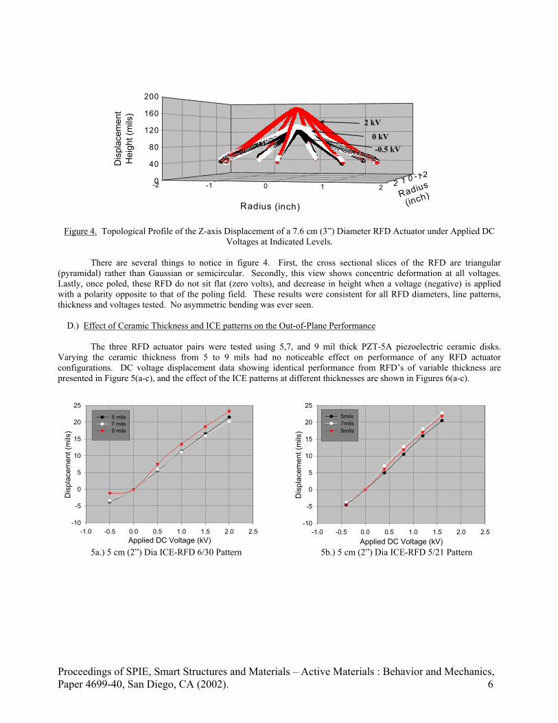
C.) RFD’s Topological Profile as a Function of Applied Voltage
Since the RFD’s advantage over other piezoelectric devices is its ability to move out of plane, we wish to
characterize the RFD’s out-of-plane displacement as a function of voltage. The topological profiles, including the neutral or 0 volts DC, of the out-of-plane displacement of a RFD under increasingly applied DC voltages from (-0.5 to 2 kV). This data was taken with the devices mechanically constrained about their perimeter. This assures better correlation between experimentally determined results and real world applications, and eliminates the complexities of modal behavior and mechanical resonance. A sample topographical profile of a 7.6 cm (3”) diameter ICE-RFD at –0.5, 0, and 2 kV is shown in Figure 4.
Proceedings of SPIE, Smart Structures and Materials – Active Materials : Behavior and Mechanics, Paper 4699-40, San Diego, CA (2002). 5
0
40
80
120
160
200
-2-1012-2 -1 0 1 2
Dis
plac
emen
tH
eigh
t (m
ils)
Radius
(inch)Radius (inch)
-0.5 kV 0 kV
2 kV
Figure 4. Topological Profile of the Z-axis Displacement of a 7.6 cm (3”) Diameter RFD Actuator under Applied DC
Voltages at Indicated Levels.
There are several things to notice in figure 4. First, the cross sectional slices of the RFD are triangular (pyramidal) rather than Gaussian or semicircular. Secondly, this view shows concentric deformation at all voltages. Lastly, once poled, these RFD do not sit flat (zero volts), and decrease in height when a voltage (negative) is applied with a polarity opposite to that of the poling field. These results were consistent for all RFD diameters, line patterns, thickness and voltages tested. No asymmetric bending was ever seen. D.) Effect of Ceramic Thickness and ICE patterns on the Out-of-Plane Performance The three RFD actuator pairs were tested using 5,7, and 9 mil thick PZT-5A piezoelectric ceramic disks. Varying the ceramic thickness from 5 to 9 mils had no noticeable effect on performance of any RFD actuator configurations. DC voltage displacement data showing identical performance from RFD’s of variable thickness are presented in Figure 5(a-c), and the effect of the ICE patterns at different thicknesses are shown in Figures 6(a-c).
Applied DC Voltage (kV)-1.0 -0.5 0.0 0.5 1.0 1.5 2.0 2.5
Dis
plac
emen
t (m
ils)
-10
-5
0
5
10
15
20
25
5 mils7 mils9 mils
Applied DC Voltage (kV)-1.0 -0.5 0.0 0.5 1.0 1.5 2.0 2.5
Dis
plac
emen
t (m
ils)
-10
-5
0
5
10
15
20
255mils7mils9mils
5a.) 5 cm (2”) Dia ICE-RFD 6/30 Pattern 5b.) 5 cm (2”) Dia ICE-RFD 5/21 Pattern
Proceedings of SPIE, Smart Structures and Materials – Active Materials : Behavior and Mechanics, Paper 4699-40, San Diego, CA (2002). 6

Applied DC Voltage (kV)-0.5 0.0 0.5 1.0 1.5 2.0 2.5
Dis
plac
emen
t (m
ils)
-10
-5
0
5
10
15
20
255mils7mils9mils
5c.) 5 cm (2”) Dia ICE-RFD 4/12 Pattern
Figure 5(a-c). Displacements of 5,7, and 9 mil thick RFD Line Configurations under a DC Applied Voltage.
Figure 6(a-c).
6a.) 5 mil thick 5 cm (2”) Dia ICE RFD Applied DC Voltage (kV)
-1.0 -0.5 0.0 0.5 1.0 1.5 2.0 2.5
Dis
plac
emen
t (m
ils)
-10
-5
0
5
10
15
20 6/305/214/12
6b.) 7 mil thick 5 cm (2”) Dia ICE RFD Applied DC Voltage (kV)
-1.0 -0.5 0.0 0.5 1.0 1.5 2.0 2.5
Dis
plac
emen
t (m
ils)
-10
-5
0
5
10
15
20 6/305/214/12
2525
6c.) 7 mil thick 5 cm (2”) Dia ICE RFD Applied DC Voltage (kV)
-1.0 -0.5 0.0 0.5 1.0 1.5 2.0 2.5
Dis
plac
emen
t (m
ils)
-10
-5
0
5
10
15
20 6/305/214/12
25
Displacements of 6/30, 5/21 and 4/12 Line Patterns as a Function of RFD Ceramic Thickness under a DC Applied Voltage.
Proceedings of SPIE, Smart Structures and Materials – Active Materials : Behavior and Mechanics, Paper 4699-40, San Diego, CA (2002). 7

E.) Effect of RFD diameter on the out-of-plane performance
to low applied voltages. Also, the topo raphy of the RFD grows linearly out of plane in response to low applied voltages and is shown in Figure 4. This
ometr
tions show in figures 7 and 8. The resulting total displacements were divided by e total
Figure 7
The ICE RFD exhibits a linear increase in displacement in response g
ge ic relationship at low applied voltages implies that an increase in the RFD diameter will produce a linear increase in out-of-plane displacement. The out of plane displacement of 1, 2, and 3 inch RFDs with 6/30, 5/21, and 4/12 electrode patterns were measured under the same voltage condith DC Vp-p to compare the RFD’s electromechanical efficiency as a function of ICE patterns. As expected, the RFDs showed a linear increase in displacement with increasing disk diameter, and as previously demonstrated in the near linear slopes of figures 5a-c, the lower the line spacing ratio (center-to-center spacing / line width) the higher the efficiency. The results are presented in Figure 7. 30
. RFD Out-of-Plane Displacement vs. Disk Diameter at Constant Electric Field.
RFD Diameter (inches)0 1 2 3 4
Dis
plac
emen
t (m
ils/k
V)
0
5
10
15
20
256/30 ICE 2.5 kVpp DC 5/21 ICE 1.8 kVpp DC 4/12 ICE 1.3 kVpp DC
F.) RFD Internal Strain Field
several RFD electrode patterns were measured. All RFD electrode patterns induce a imilar strain field into the ceramic with the only difference being an increase in strain field intensity with decreasing
d. The strain gauge setup and actual test article are shown in Figure 10 where the all “∟
The internal strain fields ofselectrode spacing. This is expected as decreasing the distance between electrodes increases the electric field strength, at a given voltage, within the ceramic. Strain measurements of the RFD were taken in the radial and tangential directions i.e. parallel and perpendicular to the radial electric fielsm ” patterns represent radial and tangential strain gauges. Fifteen strain measurements were taken both in the tangential and radial directions with gauges fourteen and fifteen placed beyond the ceramic disk. Since the RFD is circular, it can be assumed that the strain field is symmetric about the RFD as evidenced in the topological profile in Figure 4. The elliptical pattern for the gauge layout was selected for convenience only.
Proceedings of SPIE, Smart Structures and Materials – Active Materials : Behavior and Mechanics, Paper 4699-40, San Diego, CA (2002). 8

XY-StrainGauges
Piezoceramic Boundary
Tangential Strain Gauge Directions
Radial Electric Field and Radial Strain Gauge Directions
Figure 8. ICE-RFD Strain Gauge Setup. A 0.1 Hz sinusoidal voltage signal was applied to the RFD and both the radial and tangential strains were recorded. The strain measurements over four cycles were recorded and averaged. Each strain gauge produced a hysteresis loop similar to the one presented in Figure 9a. A linear approximation of each hysteresis loop was calculated and values were picked off from the linear fit at applied voltages of –500, 0, 500, 1000, 1500 and 2000 (est.) DC volts. This process was repeated for all 30 strain gauge hysteresis loops. These linear strain approximations were then plotted vs. their radial location on the RFD, an example is shown in Figure 9b. Repeating this process for the remaining strain gauges creates radial and tangential strain profiles along the radius of the RFD. The radial and tangential strain profiles for 6/30 and 5/21 electrode patterns are presented in Figures 9c and 9d respectively.
9a.) Linear Approximation of Strain Loop 9b.) Plotting Data Points vs. Radial Location Applied Voltage (kV)
-1.0 -0.5 0.0 0.5 1.0 1.5 2.0
Stra
in (p
pt)
-1.0
-0.8
-0.6
-0.4
-0.2
0.0
0.2
0.4
0.6
Radial StrainTangential StrainLinear Regression Fit
Radial Distance from Center (in)0.0 0.5 1.0 1.5 2.0
Stra
in (p
pt)
-1.0
-0.8
-0.6
-0.4
-0.2
0.0
0.2
0.4
0.6
-500 V0 V500 V1000 V1500 V2000 V
Proceedings of SPIE, Smart Structures and Materials – Active Materials : Behavior and Mechanics, Paper 4699-40, San Diego, CA (2002). 9

Radial Distance from Center (in)
0.0 0.5 1.0 1.5
Rad
ial S
train
(ppt
)
-2.5
-2.0
-1.5
-1.0
-0.5
0.0
0.5
1.0
-0.5 kV0 kV0.5 kV1 kV1.5 kV2 kV
Ceramic/FilmBoundary
2.0Radial Distance from Center (in)
0.0 0.5 1.0 1.5 2.0
Tang
entia
l Stra
in (p
pt)
-1.5
-1.0
-0.5
0.0
0.5
-0.5 kV0 kV0.5 kV1 kV1.5 kV2 kV
Ceramic/FilmBoundary
9c.) Radial and Tangential Strain Profiles for a 6/30 Electrode Patterned RFD.
Radial Distance from Center (in)0.0 0.5 1.0 1.5 2.0
Tang
entia
l Stra
in (p
pt)
-1.5
-1.0
-0.5
0.0
0.5
-500 V0 V500 V1000 V1500 V2000 V
Ceramic/FilmBoundary
Radial distance from center (in)0.0 0.5 1.0 1.5 2.0
Rad
ial S
train
(ppt
)
-2.5
-2.0
-1.5
-1.0
-0.5
0.0
0.5
1.0
-500 V0 V500 V1000 V1.5 kV2000 V
Ceramic/FilmBoundary
9d.) Tangential Strain Profiles for a 5/21 Electrode Patterned RFD.
Figure 9(a-d). RFD Radial and Tangential Strain Profiles
The above localized radial and tangential strain field results are unexpected. It is important to realize that the trends in the resulting strain fields are reproducible (as demonstrated), independent of line pattern (except in magnitude) and do lend some insight into the unexpected deformation characteristics of the RFDs. The first thing to indicate is that the data points are connected by a spline fit and that these points do not create a smooth contour. This can be explained as some of these gauges span one or more electrodes, which are physical bumps beneath the gauges, resulting in some local alteration of the strain field. Also notice that the strain field drops to almost zero at two places, beyond the ceramic boundary (radial and tangential) and at an inflection point approximately 1 cm (~0.25 in) from the center. What appears to be occurring is that as a voltage is applied in the same polarity as the poling polarity, the RFD circumference shrinks (negative strain) and the radial strain goes from negative through zero to positive within the ceramic. The effects are reversed when a voltage opposite to the poling polarity is applied. The effect of this and other evidence leads to the conclusion that the global radial strain is approximately zero, the inflection point does not shift, the tangential strains are relatively constant (at the same voltage level) across the radius of the ceramic disk and the strain levels beyond the ceramic are negligible. Thus, the almost straight-edged pyramidal shape of the RFD (Figure 4) may be attributed to the linear tangential strain field, while the minimal strain level beyond the ceramic disk can be attributed to the nearly zero global radial strain and the rapid drop off of the tangential strain. These results lend credibility to the initial observation that the circumference of the ceramic disk remains relatively constant as the RFD actuates, and that it is not a bender.
G.) RFD Low Frequency Response
Out of plane displacement of the RFD at low frequencies was also investigated. RFD frequency response of each electrode pattern was tested at frequencies ranging from DC to 10 Hz along with a commercially available circular
Proceedings of SPIE, Smart Structures and Materials – Active Materials : Behavior and Mechanics, Paper 4699-40, San Diego, CA (2002). 10
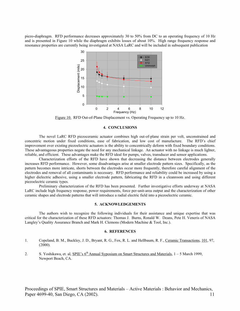
piezo-diaphragm. RFD performance decreases approximately 30 to 50% from DC to an operating frequency of 10 Hz and is presented in Figure 10 while the diaphragm exhibits losses of about 10%. High range frequency response and resonance properties are currently being investigated at NASA LaRC and will be included in subsequent publication
Frequency (Hz)0 2 4 6 8 10 1
Dis
plac
emen
t (m
ils)
0
5
10
15
20
25
306/305/214/12Unimorph
2
Figure 10. RFD Out-of-Plane Displacement vs. Operating Frequency up to 10 Hz.
4. CONCLUSIONS
The novel LaRC RFD piezoceramic actuator combines high out-of-plane strain per volt, unconstrained and concentric motion under fixed conditions, ease of fabrication, and low cost of manufacture. The RFD’s chief improvement over existing piezoelectric actuators is the ability to concentrically deform with fixed boundary conditions. These advantageous properties negate the need for any mechanical linkage. An actuator with no linkage is much lighter, reliable, and efficient. These advantages make the RFD ideal for pumps, valves, transducer and sensor applications.
Characterization efforts of the RFD have shown that decreasing the distance between electrodes generally increases RFD performance. However, some disadvantages arise at smaller electrode pattern sizes. Specifically, as the pattern becomes more intricate, shorts between the electrodes occur more frequently, therefore careful alignment of the electrodes and removal of all contaminants is necessary. RFD performance and reliability could be increased by using a higher dielectric adhesive, using a smaller electrode pattern, fabricating the RFD in a cleanroom and using different piezoelectric ceramic types.
Preliminary characterization of the RFD has been presented. Further investigative efforts underway at NASA LaRC include high frequency response, power requirements, force per-unit-area output and the characterization of other ceramic shapes and electrode patterns that will introduce a radial electric field into a piezoelectric ceramic.
5. ACKNOWLEDGEMENTS
The authors wish to recognize the following individuals for their assistance and unique expertise that was critical for the characterization of these RFD actuators: Thomas J. Burns, Ronald W. Deans, Pete H. Veneris of NASA Langley’s Quality Assurance Branch and Mark H. Clemons (Modern Machine & Tool, Inc.).
6. REFERENCES 1. Copeland, B. M., Buckley, J. D., Bryant, R. G., Fox, R. L. and Hellbaum, R. F., Ceramic Transactions, 101, 97,
(2000). 2. S. Yoshikawa, et. al, SPIE’s 6th Annual Syposium on Smart Structures and Materials, 1 – 5 March 1999,
Newport Beach, CA.
Proceedings of SPIE, Smart Structures and Materials – Active Materials : Behavior and Mechanics, Paper 4699-40, San Diego, CA (2002). 11
3. W. K. Wilkie, R. G. Bryant, J. W. High, R. L. Fox, R. F. Hellbaum, A. Jalink, Jr., B. D. Little, P. H. Mirick, Proceedings of the SPIE – Smart Structures and Materials: Industrial and Commercial Appl. Of Smart Structures Tech., 3991, 323, (2000).
4. Jaffe, B., Cook, W. R., Jr., and Jaffe, H., Piezoelectric Ceramics, Academic Press Ltd., 1971.
Proceedings of SPIE, Smart Structures and Materials – Active Materials : Behavior and Mechanics, Paper 4699-40, San Diego, CA (2002). 12