12/4/2002 Clocking – Lecture 2 and 3 Purpose – Clocking Design Topics Read Chapter 12.

17-1
A Wide Tuning Range (1 GHz-to-15 GHz) Fractional-N
All-Digital PLL in 45nm SOI
Alexander Rylyakov1, Jose Tierno1, George English2, Michael Sperling2, Daniel Friedman1
1 IBM T. J. Watson Research CenterYorktown Heights, NY 10598 USA2 IBM , Poughkeepsie, NY

Outline• Motivation• Review of DPLL linear model• DPLL architecture, digital design details • Measurement results• Conclusion

Digital PLL Advantages• Uses primarily technology elements of digital
designs, simplifies technology support and should make yield profile match that of logic
• Enables extensive use of digital flows for design and verification, offers enhanced controllability and adaptability
• Compact: no explicit filter capacitor• Ideal for ASIC, processor or any digital
clocking application, where period jitter is the key metric

Charge-pump PLL vs BB-DPLL
Linear PFD
Continuously tuned VCO
Continuous-time
Bang-bang PFD
Discrete DCO
Discrete-time
BB PFDFref
LF DCO
÷N
Fout
σπ1
21
=PFDK1
1
1 −
−
−+
zzKK IP 11 −− z
KDCO
Ffbk
π2CPI
PFD+CPFref
LF VCO
÷N
Fout
Ffbk
CsR 1+
sKVCO

Bang-bang PFD LinearizationBB PFD
±1= sign(Φref - Φfbk)
Φfbk
Φref+1
-1Φref - Φfbk
Φref
σπ1
21
=PFDKΦfbk
KPFD ePFD
+Φref
Φfbk-
Φref - Φfbk KPFD*(Φref - Φfbk) + ePFD
Assumptions:
Gaussian jitter
uncorrelated quantization noise Razavi 2004

Proportional-Integral Loop Filter
1
1
1 −
−
−zzKI
1
1
1)( −
−
−+=
zzKKzH IP
ICP VCTRL
CsRsZ 1)( +=
RC
PK
1
1111 −
−−=⇒+=+≈=TzzssTTjez Tj ωω
(ωT << 1 )
CTKI =1
1
11
−
−
−+=+
zz
CTR
CsR RKP =⇒
analog and digital proportional-integral loop filters
are equivalent
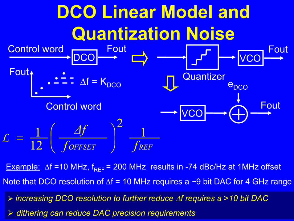
DCO Linear Model and Quantization NoiseDCO
Control word Fout
∆f = KDCO
VCOFout
Fout • Quantizer•• eDCO• •
FoutControl wordVCO
REFOFFSET ff∆f 1
2
121
=L
Example: ∆f =10 MHz, fREF = 200 MHz results in -74 dBc/Hz at 1MHz offset
Note that DCO resolution of ∆f = 10 MHz requires a ~9 bit DAC for 4 GHz range
increasing DCO resolution to further reduce ∆f requires a >10 bit DAC
dithering can reduce DAC precision requirements

Linear Model of the BB-DPLL
BB PFDFref
LF DCO
÷N
Fout
1
1
1 −
−
−+
zzKK IPσπ
121
=PFDK11 −− z
KDCO
Ffbk
Noise sources:
Quantization noise of the bang-bang PFD
Quantization noise of the DCO
Phase noise of the oscillator
Quantization noise of the feedback divider (fractional-N)
Kratyuk 2007, Hanumolu 2007, Da Dalt 2008

Bode Magnitude Plot
105 106 107 108
Frequency [Hz]
Mag
nitu
de [d
B]
5
0
-5
Fref=200 MHz
N = 20
σ = 4 ps
KP = 0.75
KI = 2-8
KDCO= 20 MHz
linear model reflects the main features of the measured phase noise: high bandwidth (~ 40 MHz), limit cycle (~ 7 dB peaking)
not a substitute of full VHDL or Verilog time-domain simulation with noise, but useful for ballpark estimates
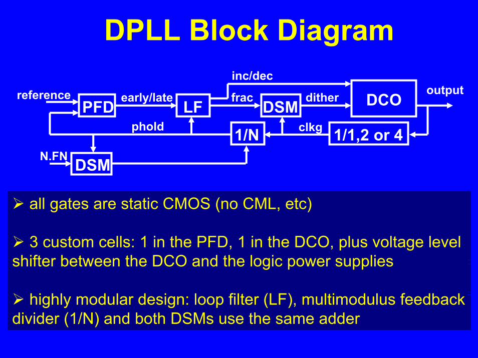
DPLL Block Diagram
PFD LF DCO
1/N 1/1,2 or 4clkg
DSM
referenceDSM
phold
ditherearly/late frac
N.FN
inc/decoutput
all gates are static CMOS (no CML, etc)
3 custom cells: 1 in the PFD, 1 in the DCO, plus voltage level shifter between the DCO and the logic power supplies
highly modular design: loop filter (LF), multimodulus feedback divider (1/N) and both DSMs use the same adder

Loop Filter
+I+P+I-P-I
-I
11
10
01
00
2
integral: 1 X 1 – z-11
proportional: (1 – z-1) X 1 – z-11
Realized Transfer Functions
Late 8 88
Inc
P = Proportional constantI = Integral constant
Dec
8FractionalFrequency
8-bit arithmetic realizedusing Kogge-Stone adder
merging proportional, integral paths simplifies DPLL logic

DCO Dithering
time
instantaneous frequencyf+∆f
FVCO
effective frequency
f
DITHOFFSET ff∆f 1
2
121
=LUniform dithering:
-81 dBc/Hz at 1MHz offset, ∆f=10 MHz, fDITH=1 GHz
2sin21
2
121
∆
=
DITHDITHOFFSET ff
ff∆f π
L1st order ∆Σ dithering:
-105 dBc/Hz at 1MHz offset, ∆f=10 MHz, fDITH=1 GHz
∆Σ dithering works, but increases power dissipation, area, complexity
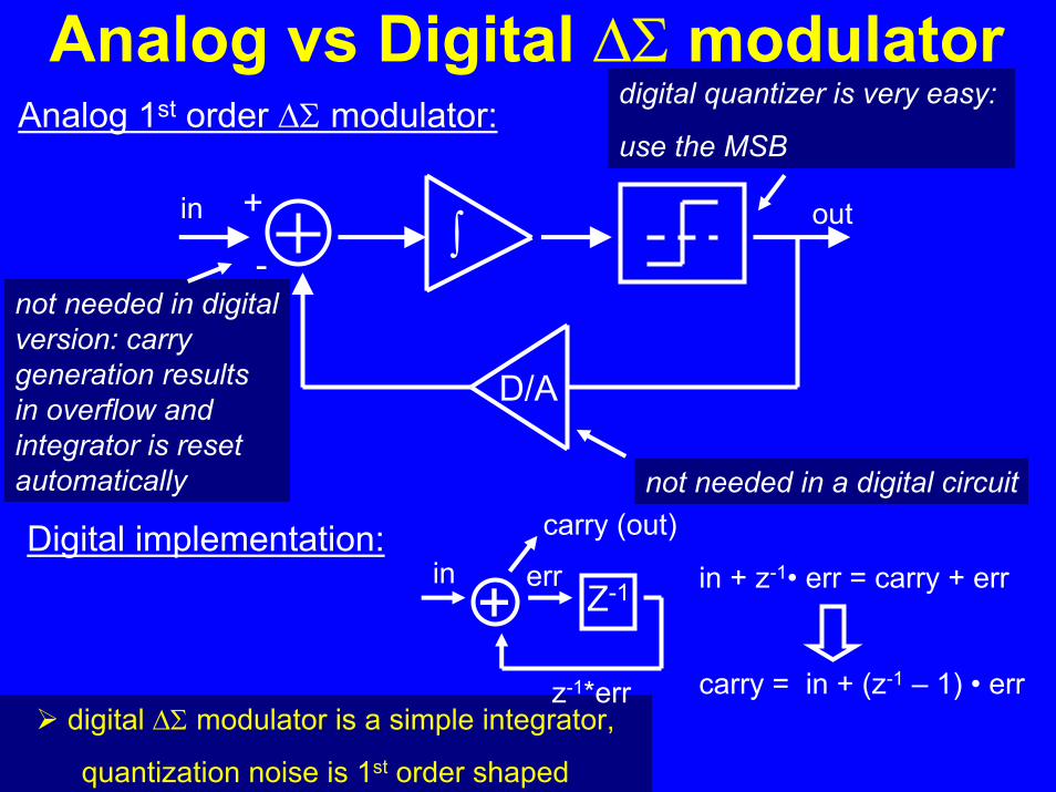
Analog vs Digital ∆Σ modulatorAnalog 1st order ∆Σ modulator:
digital quantizer is very easy:
use the MSB
digital ∆Σ modulator is a simple integrator,
quantization noise is 1st order shaped
∫-
D/A
+ Z-1in err
carry (out)
z-1*err
Digital implementation:
not needed in digital version: carry generation results in overflow and integrator is reset automatically
+in out
not needed in a digital circuit
in + z-1• err = carry + err
carry = in + (z-1 – 1) • err

Divider DSM vs DCO DSMRequires explicit 8-bit addersRequires signed arithmeticPipelining requires careful latency matching for proper noise shaping
Uses DCO as an adderGenerates DC offset (invisible due to loop action)Dithering outputs are applied in parallel with matched delays
+ Z-1 + “+”
N+FN+(z-1-1)*e1 N+FN+(z-1-1)2*e2
DCON
+ Z-1FN + Z-1
Z-1
e1
Z-1 Z-1
e2 + Z-1 + Z-1
Z-1
e1
Z-1 Z-1
e2
Z-1
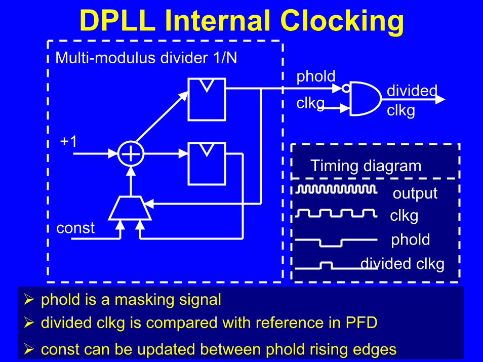
DPLL Internal Clocking
+1
const
pholdclkg
divided clkg
phold
outputclkg
divided clkg
Timing diagram
Multi-modulus divider 1/N
phold is a masking signaldivided clkg is compared with reference in PFDconst can be updated between phold rising edges

columns 1 to 48
r o w
s
1
to
16
top row
dither <1:3> outputinc/dec
inc/dec
main array
1 2 13
inv_on
row/column control
DCO Schematic
784 delay cells (73 µm x 41 µm in 45nm CMOS)this is a ~ 9.5-bit DAC

Block Diagram: Annotated
PFD LF DCO
1/N
output
1/1,2 or 4clkg
DSM
referenceDSM
inc/dec
phold
dither
-P -I
+I+P+I
-I
early/late frac
frac
N.FN
N
FN
early/late inc/dec

0
4
8
12
16
0 0.2 0.4 0.6 0.8 1
DCO Fill Factor
Freq
uenc
y [G
Hz] 1.3 V
0.7 V
1.0 V
65°C125°C
DCO Tuning Curves
covers 2 GHz to 6 GHz range across wide V,T variations

0
5
10
15
20
25
30
1 3 5 7 9 11 13 15
Frequency [GHz]
KD
CO
[MH
z pe
r ste
p]
0.7 V
1.3 V
1.0 V
15 mA5 mA 10 mA
DCO Gain vs Frequency
constant-current DCO bias enables trading off DCO tuning range for increase in DCO resolution

Period Jitter HistogramOutput: 2.06 GHz Reference: 2.06 MHz Period jitter: 2.5 ps rms, 29 ps peak to peak0.75 V, 65°C
494478Time [ps]
486
main metric for digital clocking applications: peak to peak jitter (“shortest clock cycle at a given frequency”)long term jitter (N-cycle or rms integrated from phase noise) is less of a concernphase noise purity usually not a factor

Integer and Fractional-N Period Jitter Histograms
1
260 262 264 266Time [ps]
4×4.75, 3rd order4×4.75, 1st order2×9.5, 3rd order2×9.5, 1st order1×19, no DSM
10-1
10-2
10-3
1st order DSM is adequate for digital clocking applicationsfractional-N mode could be used to save power

Fractional-N Operation at 3.6-3.8 GHz, 200 MHz reference
-200
-100
0
100
200
300
400
0 0.25 0.5 0.75 1Fractional N value
Freq
uenc
y Er
ror [
Hz]
synthesized frequency deviation from ideal: 0.12 ppm pp
limited by the sensitivity of the frequency counter

Output Spectrum at 15 GHz
-110-100
-90-80-70-60-50-40
14.95 15 15.05Frequency [GHz]
Pow
er [d
Bm
]
limited by the output driver, not by the DCO

Phase Noise at 4.1 GHz
-140
-120
-100
-80
-60
Frequency Offset [Hz]
Pow
er [d
Bc/
Hz]
104 105 106 107 108 109
high bandwidth, limit cycle are clearly visible
overall shape follows linear model predictions
acceptable for digital clocking applications

Physical Design
DCORow
ControlColumn
Control
DCO-DSMD
ivid
er-D
SM Loop Filter
Divider16
0µm
• Technology: IBM 45nm SOI CMOS
• TransistorCount: ~25k
175µm

Performance Summary
1.2 ps rms, 13.0 ps ppPeriod Jitter *
0.84 GHz – 13.3 GHz (1.0V, 65°C)1.2 GHz – 15.9 GHz (1.3V, 65°C)
Tuning Range
6.9 mWLogic
11.7 mWDCOPower Dissipation *
175 µm X 160 µmArea
45 nm SOI CMOS Technology
* at 4.12 GHz (206 MHz reference), 1.0V, 65°C

Conclusions• All static CMOS, all-digital, fractional-N PLL
demonstrated in 45 nm SOI
• Highly modular design: all key blocks (loop filter, feedback divider, DCO-DSM, divider-DSM) use instances of the same 8-bit Kogge-Stone adder
• Tuning range and period jitter performance adequate for ASIC and microprocessor clocking applications

Acknowledgements• IBM Yorktown: B. Parker, D. Kuchta, S. Gowdaand M. Soyuer
• IBM Poughkeepsie: P. Muench, G. Smith and R. Dussault
• Partial support through DARPA contract HR0011-07-9-0002