PD70210EVB PD70210 HDBT level PD Evaluation Board User Guide
16
PD70210 Evaluation Board – User Guide PD70210EVB PD70210 HDBT level PD Evaluation Board User Guide Revision 1.0 PRODUCTION DATA – Information contained in this document is proprietary to Microsemi and is current as of publication date. This document may not be modified in any way without the express written consent of Microsemi. Product processing does not necessarily include testing of all parameters. Microsemi reserves the right to change the configuration and performance of the product and to discontinue product at any time.
Transcript of PD70210EVB PD70210 HDBT level PD Evaluation Board User Guide

PD70210 Evaluation Board – User Guide
PD70210EVB
PD70210 HDBT level PD
Evaluation Board User Guide
Revision 1.0
PRODUCTION DATA – Information contained in this document is proprietary to Microsemi and is current as of publication date. This document may not be modified in any way without the express written consent of Microsemi. Product processing does not necessarily include testing of all parameters. Microsemi reserves the right to change the configuration and performance of the product and to discontinue product at any time.

PD70210 Evaluation Board – User Guide
Copyright © 2013 Microsemi Page 2 Rev. 1.0 09-Oct-13 Analog Mixed Signal Group
1 Enterprise, Aliso Viejo, CA 92656, USA; Phone (USA): (800) 713-4113, (ROW): (949) 221-7100 Fax: (949) 756-0308
Table of Contents
1 ABOUT THIS GUIDE ........................................................................................................................................ 3
1.1 Audience .................................................................................................................................................. 3
1.2 Organization ............................................................................................................................................. 3
1.3 Reference Documents ............................................................................................................................. 3
2 INTRODUCTION ............................................................................................................................................... 4
2.1 Evaluation Boards Ordering Information .................................................................................................. 5
2.2 Evaluation Board Features ...................................................................................................................... 5
3 PHYSICAL DESCRIPTION ................................................................................................................................. 6
3.1 Physical Characteristics ........................................................................................................................... 6
3.2 Package Contents .................................................................................................................................... 6
3.3 Connectors ............................................................................................................................................... 6
3.4 Indications ................................................................................................................................................ 8
4 ELECTRICAL CHARACTERISTICS ..................................................................................................................... 8
5 INSTALLATION ................................................................................................................................................ 9
5.1 Preliminary Considerations and Safety Precautions ................................................................................ 9
5.2 Initial Configuration .................................................................................................................................. 9
6 SCHEMATIC ..................................................................................................................................................10
7 LIST OF MATERIALS .....................................................................................................................................12
8 BOARD LAYOUT ...........................................................................................................................................14

PD70210 Evaluation Board – User Guide
Copyright © 2013 Microsemi Page 3 Rev. 1.0 09-Oct-13 Analog Mixed Signal Group
1 Enterprise, Aliso Viejo, CA 92656, USA; Phone (USA): (800) 713-4113, (ROW): (949) 221-7100 Fax: (949) 756-0308
1 About this Guide
This user guide provides both description and operation procedures for Microsemi's PD70210 evaluation board. This board type is used for evaluating the performance of PD70210 device.
PD70210ILD device supports both HDBT standard or standard IEEE802.3at PD application interface. The board supports a 95 Watt output at the received voltage level.
1.1 Audience
This user guide is intended for qualified personnel, that is, operators and technicians who have a background in basic concepts of electronics.
1.2 Organization
This guide is arranged according to the following:
Chapter 2 About this Guide: Describes the objectives, audience, and organization.
Chapter 2 Introduction: Provides an overview about evaluation board’s main functions, features, physical characteristics and ordering information.
Chapter 3 Physical Description: Provides explanation related to the physical description (switches, jumpers, connectors).
Chapter 4 Electrical Characteristics: Provides electrical characteristics of the evaluation board.
Chapter 5 Installation: Provides a description of the installation process.
Chapter 6 Schematic: Provides a board schematic diagram.
Chapter 7 List of Materials: Provides the board’s list of materials.
Chapter 8 Board Layout: Provides board Gerber files description for all layers.
1.3 Reference Documents
PD70210 datasheet, catalog number DS_PD70210_PD70210A

PD70210 Evaluation Board – User Guide
Copyright © 2013 Microsemi Page 4 Rev. 1.0 09-Oct-13 Analog Mixed Signal Group
1 Enterprise, Aliso Viejo, CA 92656, USA; Phone (USA): (800) 713-4113, (ROW): (949) 221-7100 Fax: (949) 756-0308
2 Introduction
Microsemi’s PD70210ILD device is part of a family of devices which are targeted for realizing the HDBT or multi 802.3at standard PD interface.
The PD interface family of devices includes the following:
Device type Power Capability Integrates PWM Controller
PD70210ILD Twin HDBT ports No
PD70210AILD Twin HDBT ports supporting Wall adapter connection
No
PD70211ILQ Twin HDBT ports supporting Wall adapter connection
Yes
Microsemi’s PD70210 Evaluation Board (see Figure 2) provides designers with the environment needed for evaluating the performance and implementation of PD applications based on PD70210 device.
The board uses a single PD device, PD70210ILD, to support the Detection, Class, and Power Supplying phases on the 2/4 Pairs of the Cat5 cable. PD70210ILD supports a standard Twin HDBT interface and compatible to IEEE802.3AT Type 2 interface.
All necessary steps and connection instructions required to install and operate this board are provided within this document.
PD70210
Based
Interface
RJ
Data
out
RJ45
Data
+
Power
Wall
adapter
In
Pulse
XFMR
Vout
conn
Active
Mosfet
Bridge
Vin
Figure 1: PD70210EVB Block Diagram

PD70210 Evaluation Board – User Guide
Copyright © 2013 Microsemi Page 5 Rev. 1.0 09-Oct-13 Analog Mixed Signal Group
1 Enterprise, Aliso Viejo, CA 92656, USA; Phone (USA): (800) 713-4113, (ROW): (949) 221-7100 Fax: (949) 756-0308
Figure 2: PD70210 Evaluation Board – General View
2.1 Evaluation Boards Ordering Information
Microsemi’s supplies the following Evaluation Boards:
Ordering Number Description
PD70210EVB IEEE802.3AT Type 2 PD, based on PD70210 device,
2.2 Evaluation Board Features
Designed to support Data and Spare current by a single PD70210 device
Input RJ45 connectors (Data and Power In)
Output voltage connector.
On board PSE type LED indicators
Evaluation Board working temperature: 0° to +70°C
RoHS compliant
PD70210 Evaluation Board – User Guide
Copyright © 2013 Microsemi Page 6 Rev. 1.0 09-Oct-13 Analog Mixed Signal Group
1 Enterprise, Aliso Viejo, CA 92656, USA; Phone (USA): (800) 713-4113, (ROW): (949) 221-7100 Fax: (949) 756-0308
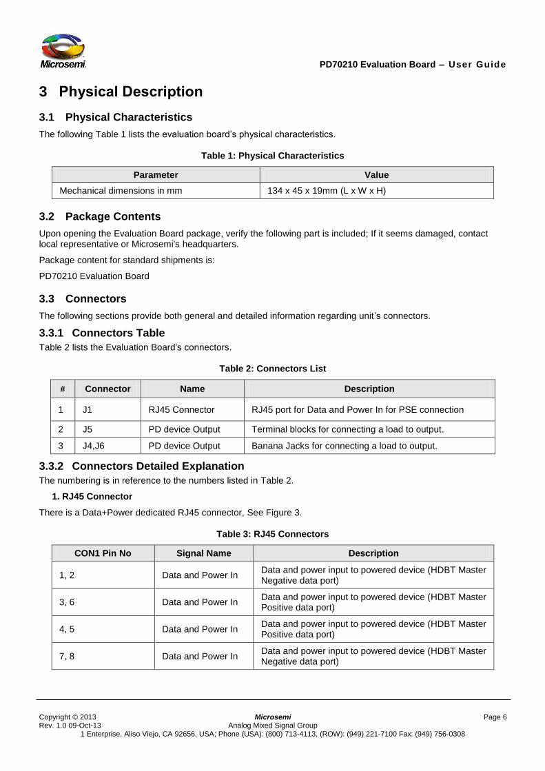
3 Physical Description
3.1 Physical Characteristics
The following Table 1 lists the evaluation board’s physical characteristics.
Table 1: Physical Characteristics
Parameter Value
Mechanical dimensions in mm 134 x 45 x 19mm (L x W x H)
3.2 Package Contents
Upon opening the Evaluation Board package, verify the following part is included; If it seems damaged, contact local representative or Microsemi's headquarters.
Package content for standard shipments is:
PD70210 Evaluation Board
3.3 Connectors
The following sections provide both general and detailed information regarding unit’s connectors.
3.3.1 Connectors Table
Table 2 lists the Evaluation Board's connectors.
Table 2: Connectors List
# Connector Name Description
1 J1 RJ45 Connector RJ45 port for Data and Power In for PSE connection
2 J5 PD device Output Terminal blocks for connecting a load to output.
3 J4,J6 PD device Output Banana Jacks for connecting a load to output.
3.3.2 Connectors Detailed Explanation
The numbering is in reference to the numbers listed in Table 2.
1. RJ45 Connector
There is a Data+Power dedicated RJ45 connector, See Figure 3.
Table 3: RJ45 Connectors
CON1 Pin No Signal Name Description
1, 2 Data and Power In Data and power input to powered device (HDBT Master Negative data port)
3, 6 Data and Power In Data and power input to powered device (HDBT Master Positive data port)
4, 5 Data and Power In Data and power input to powered device (HDBT Master Positive data port)
7, 8 Data and Power In Data and power input to powered device (HDBT Master Negative data port)

PD70210 Evaluation Board – User Guide
Copyright © 2013 Microsemi Page 7 Rev. 1.0 09-Oct-13 Analog Mixed Signal Group
1 Enterprise, Aliso Viejo, CA 92656, USA; Phone (USA): (800) 713-4113, (ROW): (949) 221-7100 Fax: (949) 756-0308
Figure 3: Front RJ45 Connector
2. Vout Connectors
See Figure 4.
J5 –output connection, used for connecting to external load.
For easy connection, Black and Red Banana jacks are parallel to J5 connections.
Table 4: J5 Connector (Green)
Pin No. Signal Name Description
J5 (Left)- Pin 1 Vout_Rtn Return PD received output voltage
J5 (Right)-Pin 2 Vout Positive PD received output voltage
Figure 4: Vout Connectors

PD70210 Evaluation Board – User Guide
Copyright © 2013 Microsemi Page 8 Rev. 1.0 09-Oct-13 Analog Mixed Signal Group
1 Enterprise, Aliso Viejo, CA 92656, USA; Phone (USA): (800) 713-4113, (ROW): (949) 221-7100 Fax: (949) 756-0308
3.4 Indications
The following sections provide general information regarding unit indications.
3.4.1.1 LED Indication
See Figure 5.
D14 is the Power_GOOD indication LED, a PD70210 device output signal indicating the device isolation switch is operated. In all operating state this flag is lit.
D12 is the AT_FLAG indication LED, a PD70210 device output signal indicating the device has detected a 2 finger class event from the PSE side in the class stage. The flag will be operative at 3, 4, and 6 fingers detection as well.
D10 is the 4P_AT indication LED, a PD70210 device output signal indicating the device has detected a 4 finger class event from the PSE side in the class stage, or a 2 finger class event from the PSE side in the class stage, and SUPP_Sa and SUPP_Sb are both High.
The flag will be operative at 6 fingers detection as well.
D11 is the HD_FLAG indication LED, a PD70210 device output signal indicating the device has detected a 3 finger class event from the PSE side in the class stage.
The flag will be operative at 6 fingers detection as well.
D9 is the 4P_HD indication LED, a PD70210 device output signal indicating the device has detected a 6 finger class event from the PSE side in the class stage.
Figure 5: LED Indications
4 Electrical Characteristics
Evaluation board’s electrical characteristics are described below:
Table 5: Electrical Characteristics
Parameter Min Max
RJ45 connector 38 57 V
Maximum Available Current 2.2 A

PD70210 Evaluation Board – User Guide
Copyright © 2013 Microsemi Page 9 Rev. 1.0 09-Oct-13 Analog Mixed Signal Group
1 Enterprise, Aliso Viejo, CA 92656, USA; Phone (USA): (800) 713-4113, (ROW): (949) 221-7100 Fax: (949) 756-0308
5 Installation
5.1 Preliminary Considerations and Safety Precautions
Verify board's power supply is turned off before all peripheral devices are connected.
Note: In maximum power at the output, some of the devices may reach high temperatures (still less than 70 degrees). Pay attention while testing these devices.
5.2 Initial Configuration
Note: Prior to starting any operation, it is important to verify that the Evaluation Board is setup as shown in Figure 6.
1. Connect load to main board (J5), while it is turned Off.
Notice: To comply with IEEE802.3AT standard, the load should be set only after the PSE is On.
The indication for PSE On is PGOOD led lit.
2. Connect a Cat5 cable from PSE to Evaluation Board (J1).
3. Turn On the Load.
Cat5
cable
Electronic Load
Power
CableDC output
PSE
Data +
Power
input
Cat5
cable
Figure 6: Test Setup

PD70210 Evaluation Board – User Guide
Copyright © 2013 Microsemi Page 10 Rev. 1.0 09-Oct-13 Analog Mixed Signal Group
1 Enterprise, Aliso Viejo, CA 92656, USA; Phone (USA): (800) 713-4113, (ROW): (949) 221-7100 Fax: (949) 756-0308
6 Schematic
Figure 7: Board Schematics (1 of 2)
Power_sapre-
VAUX
R1360PD-0805
N.C
R1370PD-0805
N.C
R1380PD-0805
N.C
VPNin
tp135x70HK-2-G-S05
1
VPNout
tp135x70
HK-2-G-S05
1
+ C722uF
100V
ALU
D8H12F3_5
N.C
R75
20K
PD-1206
Q18
MMBT2222ALT1
PD-SOT23
1
23 D39
BAV21WS
PD-SOD323
21D40
BZX84C8V2 LT1G
PD-SOT23
1 32
D41
BZX84C8V2 LT1G
PD-SOT23
13
2
D42
BAV21WS
PD-SOD323
2 1
C801nF
PD-0603
Power_Data-
C811nF
PD-0603
Power_sapre-
Power_sapre-
Power_sapre+
Q19
MMBT2222ALT1
PD-SOT23
1
23
D44
BZX84C8V2 LT1G
PD-SOT23
13
2
D43
BAV21WS
PD-SOD323
2 1
D46
BAV21WS
PD-SOD323
21D45
BZX84C8V2 LT1G
PD-SOT23
1 3
2
C821nF
PD-0603
C831nF
PD-0603
Q5
FMMT549
PD-SOT23
1
32
VPP
U1
PD-70210PD-DFN-16-5X4-15-v ia
VPP1
RDET2
SUPP_S13
SUPP_S24
RREF5
RCLS6
VPN_IN77
VPN_IN88
VAUX16
PGOOD15
4P_HD_FLAG14
4P_AT_FLAG13
HD_FALG12
AT_FLAG11
VPN_OUT1010
VPN_OUT99
Trm
_P
17
-
+
~~
D6SDB203
N.C
DFS-BRIDGE
2
1
3
4
D47
BAV21WS
PD-SOD323
21Q20
MMBT2222ALT1
PD-SOT23
1
23
D49
BZX84C8V2 LT1G
PD-SOT23
13
2
D48
PD-SOT23
1 3
2
D50
BAV21WS
PD-SOD323
2 1
C841nF
PD-0603D51
BAV21WS
PD-SOD323
2 1
C851nF
PD-0603
D52
PD-SOT23
1 3
2
Q21
PD-SOT23
12
3D53
BZX84C8V2 LT1G
PD-SOT23
13
2
D54
PD-SOD323
21
C861nF
PD-0603
C871nF
PD-0603
Q8
FMMT549
PD-SOT23
1
32
U17
PD-Mosf et_Dual
PD-MLP12-4_5X5
$PIN07
$PIN18
$PIN29
$PIN310
$PIN411
$PIN512
$PIN66
$PIN75
$PIN84
$PIN93
$PIN102
$PIN111
$P
IN12
13
$P
IN13
14
$P
IN14
15
$P
IN15
16
Q9
FMMT549
PD-SOT23
1
32
POWER + DATA INPUT
Power_Data-
IN6IN7IN8
IN2IN3IN4
IN5
12
34
56
78
J1
SS71800-007F
RJ45-I
1122334455667788
99
1010
IN1
T1
VP6014 LF
BEL-S558-10GB-02V
N.C
13
15
14
16
18
17
19
21
20
22
24
23
12
10
11978645312
U16
PD-Mosf et_Dual
PD-MLP12-4_5X5
$PIN07
$PIN18
$PIN29
$PIN310
$PIN411
$PIN512
$PIN66
$PIN75
$PIN84
$PIN93
$PIN102
$PIN111
$P
IN12
13
$P
IN13
14
$P
IN14
15
$P
IN15
16
Power_Data+
-
+
~~
D7SDB203
N.C
DFS-BRIDGE2
1
3
4
Power_sapre+
VPP
Q10
FMMT549
PD-SOT23
1
32
Power_Data+
SUPP_S1SUPP_S2
VPNin_BR
PGOOD1PGOOD
R324.9KPD-0603
HD_FLAG4P_AT_FLAG4P_HD_FLAG
C4100n
100V
R130.9PD-0603
VPNin_BR
4P_HD_FLAG4P_HD
14P_AT
1HD_FLAG
1AT_FLAG
1
R2
60.4K
PD-0603
PGOOD
C3
100v
100nF
N.C
+ C622uF
100V
ALU
D8H12F3_5
N.C
C21uF
R12020KPD-0603
R12220KPD-0603
R12120KPD-0603
R12320KPD-0603
RDET
R11720KPD-0603
R11620KPD-0603
R11820KPD-0603
R11920KPD-0603
R12420KPD-0603
RREF
J4CON-F602-2P571-0500
11
22
J6
CON-F602-2P571-0100
11
22
RCLASS AT_FLAG
VAUX1
D9
Super Yellow Green
21
VPP
R71
20K
PD-1206
PD-1206-W
4P_AT_FLAG
D10
Super Yellow Green
21
VPP
R72
20K
PD-1206
PD-1206-W
HD_FLAG
D11
Super Yellow Green
21
VPP
R73
20K
PD-1206
PD-1206-W
AT_FLAG
D12
Super Yellow Green
21
VPP
tp135x70HK-2-G-S05
1VPP
VPP
R74
20K
PD-1206
PD-1206-W
D14
Super Yellow Green
21
VPP
R76
20K
PD-1206
PD-1206-W
J5
11
22
33
44
VPP
D3NCN.C
21
J7
5558397-1
rj45-5
N.C
12345678
910
VPNin
VPNin
Power_sapre+
VPNout
D55BAV70
PD-SOT23
13
2
C1
100v
100nF
SUPP_S1Power_Data+
Power_Data-
D56BAV70
PD-SOT23
13
2
SUPP_S2
SW1
SW-4P
78F01S
123
4

PD70210 Evaluation Board – User Guide
Copyright © 2013 Microsemi Page 11 Rev. 1.0 09-Oct-13 Analog Mixed Signal Group
1 Enterprise, Aliso Viejo, CA 92656, USA; Phone (USA): (800) 713-4113, (ROW): (949) 221-7100 Fax: (949) 756-0308
Figure 8: Board Schematics (2 of 2)
C88
2000V
1n
X7R
Power_sapre+
Power_Data-
C37
100V10n
X7RPD-0805
Power_sapre-
C35
100V10n
X7RPD-0805
C38
100V10n
X7RPD-0805
C36
100V10n
X7RPD-0805
R13975
PD-0805
R14175
PD-0805
R14075
PD-0805
R14275
PD-0805
R790 PD-1206
R780 PD-1206
Power_Data+
J2
RAPC722X-TB13
SWITCHCRAFT-RAPC722
N.C
231
VPNin_BR
VPP
VPNin
D13PD-SMA
N.C2 1
VPNinVPNin_BR
C5100v 100nF N.C
VAUX
JP11
CVILUX-CH82-10P-V
11
223
34
455
667
78
899
1010
4P_HD_FLAG
AT_FLAG
PGOOD
HD_FLAG4P_AT_FLAG
VPNout
R1280
PD-0402
Power_Data-
IN2
R1290
PD-0402
IN1
R1300
PD-0402
IN6
Power_Data+
R1310
PD-0402
IN3
R1320
PD-0402
Power_sapre-
IN5
R1330
PD-0402
IN4
R1340
PD-0402
Power_sapre+
R1350
PD-0402
IN8
IN7

PD70210 Evaluation Board – User Guide
Copyright © 2013 Microsemi Page 12 Rev. 1.0 09-Oct-13 Analog Mixed Signal Group
1 Enterprise, Aliso Viejo, CA 92656, USA; Phone (USA): (800) 713-4113, (ROW): (949) 221-7100 Fax: (949) 756-0308
7 List of Materials
Table 6: PD70210EVB Components
Item Description Qty Ref Des Mfr Manufacturer P\N
1 HDbaseT, AF/AT PD CHIP Front End
1 U1 Microsemi PD70210ILD
2 CAP CRM 10nF 100V 5% X7R 0805 SMT
4 C35-C38 AVX 08051C103JAT2A
3 CAP CRM 1nF/2000V 10%++X7R 1206 SMT
1 C88 AVX 1206GC102KAT1A
4 CAP CRM 100nF 100V 10% X7R 1206 SMT
1 C4 AVX 12061C104KAT2A
5 Cap 1nF 100V 10% X7R 0603 SMT 8 C80-C87 Hitano 0603B102K101NT
6 Capacitor,X7R, 1uF, 25V, 10% 0603
1 C2 Murata GRM188R71E105KA12D
7 Capacitor, X7R, 100nF,100v, 10% 0603
1 C1 Murata GRM188R72A104KA35D
8 PIN HEADER 2*5 PINs SMT 0.1" PIN SQUER TIN
1 JP11 CviLux CH81-102M100-00
9 CON RJ45 SINGLE 8 POS. SHILDED
1 J1 Bel Stewart SS71800-007F
10 90o Socket 4mm Red 1 J4 Deltron 571-0500
11 90oSocket 4mm Black 1 J6 Deltron 571-0100
12 Terminal block 2 pole insert 1 J5 DINKLE DT-123RA-02P
13 DIO 200V 250mA SOD323 SMT trr=50nSEC SWI
8 D39,D42,D43,D46,D47, D50,D51,D54
Diodes Inc. BAV21WS-7-F
14 DIO DUAL 70V 200mA 250mW Trr=6nS COM. CAT SOT23
2 D55,D56 Infineon BAV70
15 DIO 8.2V 225mW 5% Ir=5uA SOT23 SMT ZENER
8 D40,D41,D44,D45,D48, D49,D52,D53
ON Semi BZX84C8V2 LT1G
16 LED SuperYelGrn 100-130o 20-40mcd h=1 0603 SMD
5 D9-D12,D14 Everlight 19-21-SYGCS530E3TR8
17 RES 75R 125mW 1% 0805 SMT 4 R139-R142 Bourns CR0805-FX-75R0-ELF
18 Resistor, 0 Ohm, 5%, 1/16W 0402 8 R128-R135 ASJ CR10-000ZK
19 RES 0R 250mW 5% 1206 SMT JUMPER<0.05R
2 R78,R79 Samsung RC3216J000CS
20 RES TK FLM 20K 250mW 1% 1206
6 R71-R76 Bourns CR1206-FX-2002-ELF
21 Resistor, 20K, 5%, 1/16W 0603 9 R116-R124 ASJ CR16-203JL
22 RES TCK FLM 24.9K 62.5mW 1% 0603 SMT
1 R3 ASJ CR16-2492FL
23 Resistor, 30.9R 1%, 1/10W 0603 1 R1 KOA RK73H1JTTD30R9

PD70210 Evaluation Board – User Guide
Copyright © 2013 Microsemi Page 13 Rev. 1.0 09-Oct-13 Analog Mixed Signal Group
1 Enterprise, Aliso Viejo, CA 92656, USA; Phone (USA): (800) 713-4113, (ROW): (949) 221-7100 Fax: (949) 756-0308
Item Description Qty Ref Des Mfr Manufacturer P\N
F
24 RES TCK FLM 60.4K 62.5mW 1% 0603 SMT
1 R2 ASJ CR16-6042FL
25 DIP SWITCH 2 Positions 1 pole 1 SW1 Grayhill 7801T
26 TRN PNP -30V -1A SOT23 4 Q5,Q8-Q10 Fairchild FMMT549
27 TRN NPN 40V 600mA SOT23 300mW
4 Q18-Q21 Diodes Inc. MMBT2222A-7-F
28 IC Dual N/P CH power mosfet 100v 6A SMT
2 U16,U17 Fairchild FDMQ8203

PD70210 Evaluation Board – User Guide
Copyright © 2013 Microsemi Page 14 Rev. 1.0 09-Oct-13 Analog Mixed Signal Group
1 Enterprise, Aliso Viejo, CA 92656, USA; Phone (USA): (800) 713-4113, (ROW): (949) 221-7100 Fax: (949) 756-0308
8 Board Layout
This paragraph presents the layout of the evaluation board.
The board is a 2 layer board. The layers are 2 Oz layers. Below figures present the two copper layers and the silk of the board for tracking devices placements.
Figure 9: Top Silk
Figure 10: Top Layer

PD70210 Evaluation Board – User Guide
Copyright © 2013 Microsemi Page 15 Rev. 1.0 09-Oct-13 Analog Mixed Signal Group
1 Enterprise, Aliso Viejo, CA 92656, USA; Phone (USA): (800) 713-4113, (ROW): (949) 221-7100 Fax: (949) 756-0308
Figure 11: Bottom Layer
Figure 12: Bottom Silk

PD70210 Evaluation Board – User Guide
Copyright © 2013 Microsemi Page 16 Rev. 1.0 09-Oct-13 Analog Mixed Signal Group
1 Enterprise, Aliso Viejo, CA 92656, USA; Phone (USA): (800) 713-4113, (ROW): (949) 221-7100 Fax: (949) 756-0308
The information contained in the document is PROPRIETARY AND CONFIDENTIAL information of Microsemi and cannot be copied, published, uploaded, posted, transmitted, distributed or disclosed or used without the express duly signed written consent of Microsemi If the recipient of this document has entered into a disclosure agreement with Microsemi, then the terms of such Agreement will also apply . This document and the information contained herein may not be modified, by any person other than authorized personnel of Microsemi. No license under any patent, copyright, trade secret or other intellectual property right is granted to or conferred upon you by disclosure or delivery of the information, either expressly, by implication, inducement, estoppels or otherwise. Any license under such intellectual property rights must be approved by Microsemi in writing signed by an officer of Microsemi.
Microsemi reserves the right to change the configuration, functionality and performance of its products at anytime without any notice. This product has been subject to limited testing and should not be used in conjunction with life-support or other mission-critical equipment or applications. Microsemi assumes no liability whatsoever, and Microsemi disclaims any express or implied warranty, relating to sale and/or use of Microsemi products including liability or warranties relating to fitness for a particular purpose, merchantability, or infringement of any patent, copyright or other intellectual property right. The product is subject to other terms and conditions which can be located on the web at http://www.microsemi.com/legal/tnc.asp
Revision History
Revision Level / Date Para. Affected/Page Description
0.1 / 07-01-13 Initial revision
1.0 / 09-10-13 updated BOM
© 2013 Microsemi Corp.
All rights reserved.
For support contact: [email protected]
Visit our web site at: www.microsemi.com Catalog Number: PD70210_UG_EVB