Pci Express Intel
8
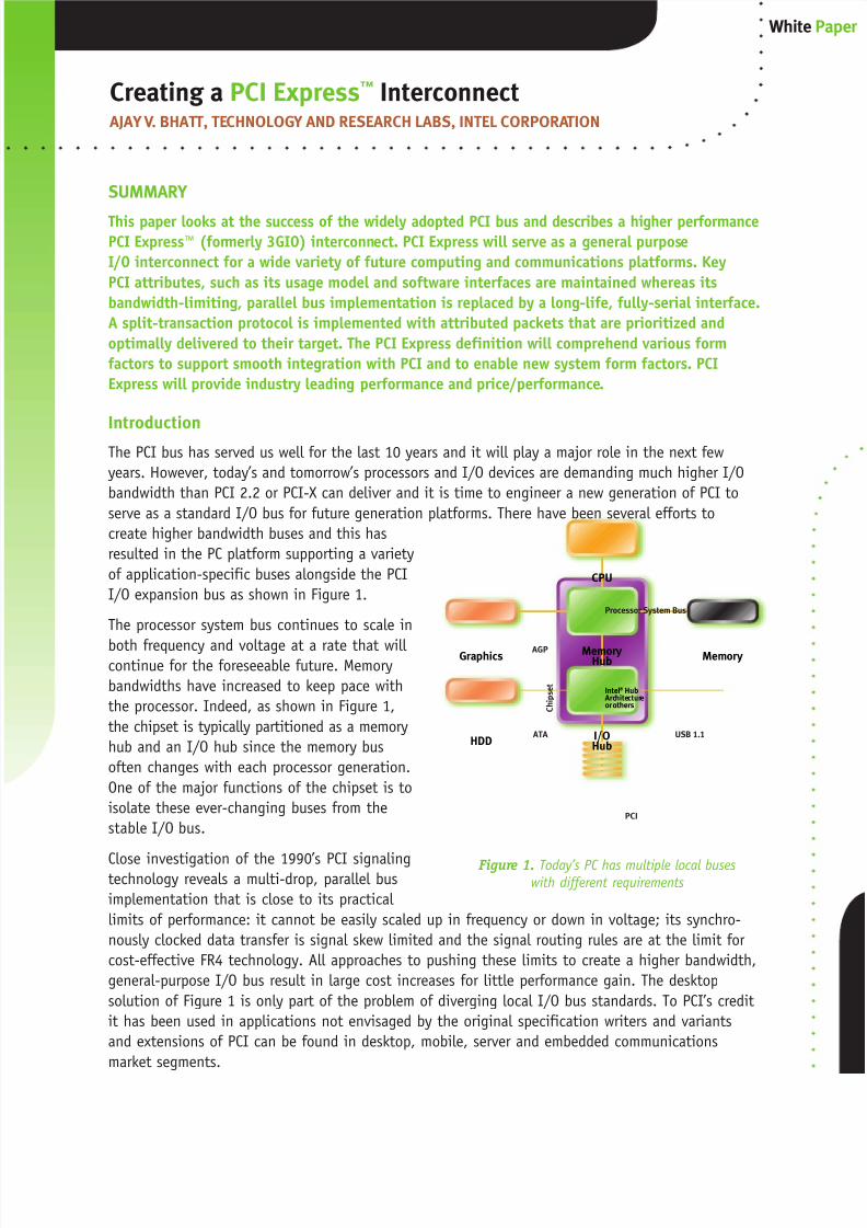
SUMMARY This paper looks at the success of the widely adopted PCI bus and describes a higher performance PCI Express™ (for merly 3GIO) interconn ect. PCI Express will serve as a general purpos e I/O interconnect for a wide variety of future computing and communications platforms. Key PCI attributes, such as its usage model and software interfaces are maintained whereas its bandwidth-limiting, parallel bus implementation is replaced by a long-life, fully-serial interface. A split-transaction protocol is implemented with attributed packets that are prioritized and optimally delivered to their target. The PCI Express definition will comprehend various form factors to support smooth integration with PCI and to enable new system form factors. PCI Express will provide industry leading performance and price/performance . Introduction The PCI bus has served us well for the last 10 years and it will play a major role in the next few years. However, today’s and tomorrow’s processors and I/O devices are demanding much higher I/O bandwidth than PCI 2.2 or PCI-X can deliver and it is time to engineer a new generation of PCI to serve as a standard I/O bus for future generation platforms. There have been several efforts to create higher bandwidth buses and this has resulted in the PC platform supporting a variety of application-specific buses alongside the PCI I/O expansion bus as shown in Figure 1. The processor system bus continues to scale in both frequency and voltage at a rate that will continue for the foreseeable future. Memory bandwidths have increased to keep pace with the processor. Indeed, as shown in Figure 1, the chipset is typically partitioned as a memory hub and an I/O hub since the memory bus often changes with each processor generation. One of the major functions of the chipset is to isolate these ever-changing buses from the stable I/O bus. Close investigation of the 1990’s PCI signaling technology reveals a multi-drop, parallel bus implementation that is close to its practical limits of performance: it cannot be easily scaled up in frequency or down in voltage; its synchro- nously clocked data transfer is signal skew limited and the signal routing rules are at the limit for cost-effective FR4 technology. All approaches to pushing these limits to create a higher bandwidth, general-purpose I/O bus result in large cost increases for little performance gain. The desktop solution of Figure 1 is only part of the problem of diverging local I/O bus standards. To PCI’s credit it has been used in applications not envisaged by the original specification writers and variants and extensions of PCI can be found in desktop, mobile, server and embedded communications market segments. CPU Graphics Memory HDD ATA PCI USB 1.1 AGP Processor System Bus Intel ® Hub Arc hite ctur e or others C h i p s e t Memory Hub I/O Hub Creating a PCI Express ™ Interconnect AJAY V . BHAT T, TECHNOLOG Y AND RESEARCH LABS, INTEL CORPORA TION Figur e 1. Today’s PC has multiple local buses with different requirements White Paper
-
Upload
ruthvin-suvarna -
Category
Documents
-
view
255 -
download
0
Transcript of Pci Express Intel
8/11/2019 Pci Express Intel
http://slidepdf.com/reader/full/pci-express-intel 1/8
SUMMARY
This paper looks at the success of the widely adopted PCI bus and describes a higher performancePCI Express™ (formerly 3GIO) interconnect. PCI Express will serve as a general purposeI/O interconnect for a wide variety of future computing and communications platforms. Key
PCI attributes, such as its usage model and software interfaces are maintained whereas itsbandwidth-limiting, parallel bus implementation is replaced by a long-life, fully-serial interface.A split-transaction protocol is implemented with attributed packets that are prioritized and
optimally delivered to their target. The PCI Express definition will comprehend various formfactors to support smooth integration with PCI and to enable new system form factors. PCIExpress will provide industry leading performance and price/performance.
IntroductionThe PCI bus has served us well for the last 10 years and it will play a major role in the next few
years. However, today’s and tomorrow’s processors and I/O devices are demanding much higher I/O
bandwidth than PCI 2.2 or PCI-X can deliver and it is time to engineer a new generation of PCI to
serve as a standard I/O bus for future generation platforms. There have been several efforts to
create higher bandwidth buses and this has
resulted in the PC platform supporting a variety
of application-specific buses alongside the PCI
I/O expansion bus as shown in Figure 1.
The processor system bus continues to scale in
both frequency and voltage at a rate that will continue for the foreseeable future. Memory
bandwidths have increased to keep pace with
the processor. Indeed, as shown in Figure 1,
the chipset is typically partitioned as a memory
hub and an I/O hub since the memory bus
often changes with each processor generation.
One of the major functions of the chipset is to
isolate these ever-changing buses from the
stable I/O bus.
Close investigation of the 1990’s PCI signalingtechnology reveals a multi-drop, parallel bus
implementation that is close to its practical
limits of performance: it cannot be easily scaled up in frequency or down in voltage; its synchro-
nously clocked data transfer is signal skew limited and the signal routing rules are at the limit for
cost-effective FR4 technology. All approaches to pushing these limits to create a higher bandwidth,
general-purpose I/O bus result in large cost increases for little performance gain. The desktop
solution of Figure 1 is only part of the problem of diverging local I/O bus standards. To PCI’s credit
it has been used in applications not envisaged by the original specification writers and variants
and extensions of PCI can be found in desktop, mobile, server and embedded communications
market segments.
CPU
Graphics Memory
HDD ATA
PCI
USB 1.1
AGP
Processor System Bus
Intel® Hub Architectureor others
C h i p s e t
Memory Hub
I/OHub
Creating a PCI Express™ Interconnect AJAY V. BHATT, TECHNOLOGY AND RESEARCH LABS, INTEL CORPORATION
Figure 1. Today’s PC has multiple local buseswith different requirements
White Pap
8/11/2019 Pci Express Intel
http://slidepdf.com/reader/full/pci-express-intel 2/8
2
Today’s software applications are more demandingof the platform hardware, particularly the I/O
subsystems. Streaming data from various video
and audio sources are now commonplace on the
desktop and mobile machines and there is no
baseline support for this time-dependent data
within the PCI 2.2 or PCI-X specifications.
Applications such as video-on-demand and audio
redistribution are putting real-time constraints on
servers too. Many communications applications
and embedded-PC control systems also process
data in real time. Today’s platforms, an exampledesktop PC is shown in Figure 2, must also
deal with multiple concurrent transfers at ever-
increasing data rates. It is no longer acceptable
to treat all data as equal—it is more important,
for example, to process streaming data first since
late real-time data is as useless as no data. Data
needs to be “tagged” so that an I/O system can
prioritize its flow throughout the platform.
Applications, such as Gigabit Ethernet* and
InfiniBand*, require higher bandwidth I/O. APCI Express bus must include additional features
alongside increased bandwidth.
REQUIREMENTS FOR A THIRD GENERATION
GENERAL PURPOSE I/O INTERCONNECT
Supports multiple market segments and
emerging applications: Unifying I/O Architecture
for Desktop, Mobile, Server, Communications
Platforms, Workstations and Embedded Devices.
Low cost and high
volume: Cost at or below
PCI cost structure at the
system level.
PCI Compatible software
model: Boot existing
operating systems without
any change. PCI compat-
ible configuration and
device driver interfaces.
Performance: Scalable
performance via frequency
and additional lanes. High
Bandwidth per Pin. Low
overhead. Low latency.
Support multiple platform connection types:
Chip-to-chip, board-to-board via connector,
docking station and enable new form factors.
Advanced features: Comprehend different data
types. Power Management. Quality Of Service.
Hot Plug and Hot Swap support. Data Integrity
and Error Handling. Extensible. Base mecha-
nisms to enable Embedded and Communications
applications.
Non-Goals: Coherent interconnect for processors,memory interconnect, cable interconnect for
cluster solutions.
PCI
I/O Bridge
Ethernet*
Graphics
CPU
M
e m o r y
HostBridge
SATA
USB2
LPC
Figure 2. Multiple concurrent data transfers.
Memory End Point
End Point End Point
End PointEnd Point
End PointEnd Point
End Point
CPU
HostBridge
Switch
Figure 3. A switch is added to the system topology.
8/11/2019 Pci Express Intel
http://slidepdf.com/reader/full/pci-express-intel 3/8
PCI Express™ Overview
Recent advances in high-speed, low-pin-count,
point-to-point technologies offer an attractive
alternative for major bandwidth improvements.
A PCI Express topology contains a Host Bridge
and several endpoints (the I/O devices) as
shown in Figure 3. Multiple point-to-point
connections introduce a new element, the
switch, into the I/O system topology also shown
in Figure 3. The switch replaces the multi-drop
bus and is used to provide fan-out for the I/O
bus. A switch may provide peer-to-peer commu-
nication between different endpoints and this
traffic, if it does not involve cache-coherent
memory transfers, need not be forwarded to the
host bridge. The switch is shown as a separatelogical element but it could be integrated into
a host bridge component.
The low signal-count, point-to-point connections
may be constructed with connectors and cables.
The PCI Express mechanicals will enable new
classes of system partitioning (the “boring beige
box” is no longer required!).
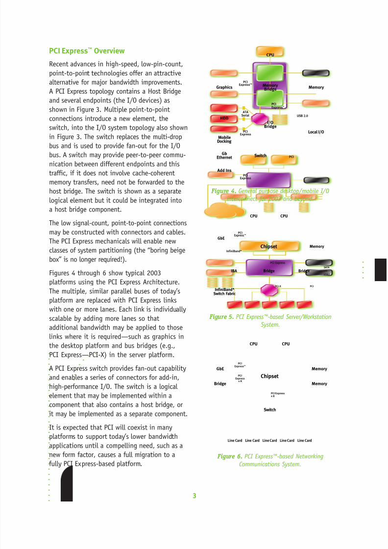
Figures 4 through 6 show typical 2003
platforms using the PCI Express Architecture.
The multiple, similar parallel buses of today’s
platform are replaced with PCI Express links
with one or more lanes. Each link is individually
scalable by adding more lanes so that
additional bandwidth may be applied to those
links where it is required—such as graphics in
the desktop platform and bus bridges (e.g.,
PCI Express—PCI-X) in the server platform.
A PCI Express switch provides fan-out capability
and enables a series of connectors for add-in,
high-performance I/O. The switch is a logical element that may be implemented within a
component that also contains a host bridge, or
it may be implemented as a separate component.
It is expected that PCI will coexist in many
platforms to support today’s lower bandwidth
applications until a compelling need, such as a
new form factor, causes a full migration to a
fully PCI Express-based platform.
3
CPU
Graphics Memory
GbEthernet
MobileDocking
ATA Serial
PCIExpress
PCIExpress
PCIExpress™
PCIExpress™
Memory Bridge
USB 2.0
PCI
HDD
Local I/O
Add Ins
I/OBridge
Switch
Figure 4. General purpose desktop/mobile I/Ointerconnect for 2003 and beyond.
Memory
Memory
GbE
PCIExpress™
Bridge
PCIExpress
x 8
PCI Express x 8
CPUCPU
Chipset
Switch
Line CardLine CardLine Card Line CardLine Card
Figure 6. PCI Express™-based Networking
Communications System.
SATA
USB2
LFC
Memory
GbE
PCIExpress™
InfiniBand*
IBA
CPUCPU
PCI-X
PCI Express
PCI
BridgeBridge
Chipset
InfiniBand*Switch Fabric
Figure 5. PCI Express™-based Server/Workstation
System.
8/11/2019 Pci Express Intel
http://slidepdf.com/reader/full/pci-express-intel 4/8
The server platform requires more I/O perfor-mance and connectivity including high-
bandwidth PCI Express links to PCI-X slots,
Gigabit Ethernet and an InfiniBand fabric. Figure
5 shows how PCI Express provides many of the
same advantages for servers, as it does for
desktop systems. The combination of PCI Express
for “inside the box” I/O, and InfiniBand fabrics
for “outside the box” I/O and cluster intercon-
nect, allows servers to transition from “parallel
shared buses” to high-speed serial interconnects.
The networking communications platform could
use multiple switches for increased connectivity
and Quality Of Service for differentiation of
different traffic types. It too would benefit
from a multiple PCI Express links that could be
constructed as a modular I/O system.
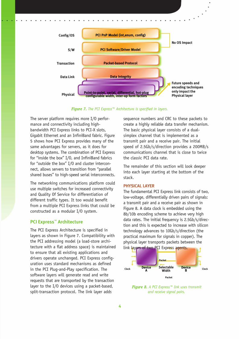
PCI Express™ Architecture
The PCI Express Architecture is specified in
layers as shown in Figure 7. Compatibility withthe PCI addressing model (a load-store archi-
tecture with a flat address space) is maintained
to ensure that all existing applications and
drivers operate unchanged. PCI Express config-
uration uses standard mechanisms as defined
in the PCI Plug-and-Play specification. The
software layers will generate read and write
requests that are transported by the transaction
layer to the I/O devices using a packet-based,
split-transaction protocol. The link layer adds
sequence numbers and CRC to these packets tocreate a highly reliable data transfer mechanism.
The basic physical layer consists of a dual-
simplex channel that is implemented as a
transmit pair and a receive pair. The initial
speed of 2.5Gb/s/direction provides a 200MB/s
communications channel that is close to twice
the classic PCI data rate.
The remainder of this section will look deeper
into each layer starting at the bottom of the
stack.
PHYSICAL LAYER
The fundamental PCI Express link consists of two,
low-voltage, differentially driven pairs of signals:
a transmit pair and a receive pair as shown in
Figure 8. A data clock is embedded using the
8b/10b encoding scheme to achieve very high
data rates. The initial frequency is 2.5Gb/s/direc-
tion and this is expected to increase with silicon
technology advances to 10Gb/s/direction (the
practical maximum for signals in copper). Thephysical layer transports packets between the
link layers of two PCI Express agents.
4
PCI PnP Model (int,enum, config)
PCI Software/Driver Model
Packet-based Protocol
Data Integrity
Point-to-point, serial, differential, hot-plug configurable width, inter-op form factors
Config/OS
Physical
Data Link
Transaction
No OS Impact
Future speeds andencoding techniquesonly impact thePhysical layer
S/W
Figure 7. The PCI Express™ Architecture is specified in layers.
Device A
DeviceB
SelectableWidth
Packet
Packet
Clock Clock
Figure 8. A PCI Express™ link uses transmit
and receive signal pairs.
8/11/2019 Pci Express Intel
http://slidepdf.com/reader/full/pci-express-intel 5/8
5
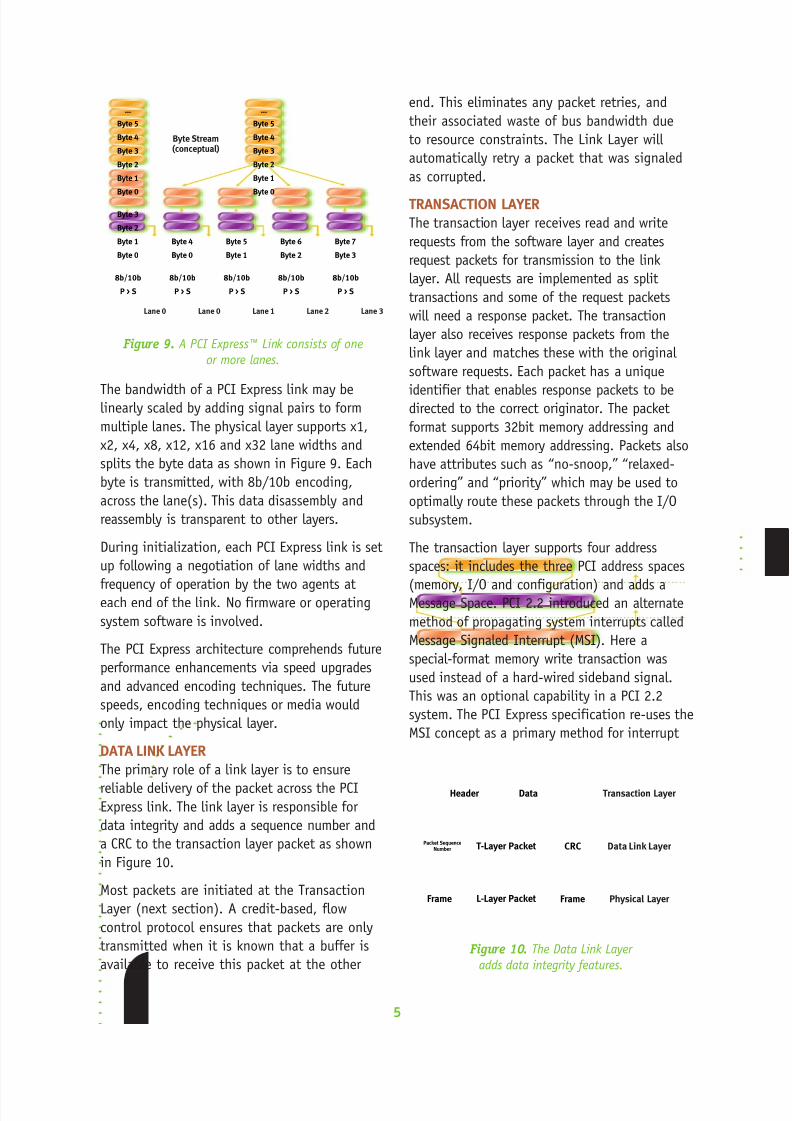
The bandwidth of a PCI Express link may belinearly scaled by adding signal pairs to form
multiple lanes. The physical layer supports x1,
x2, x4, x8, x12, x16 and x32 lane widths and
splits the byte data as shown in Figure 9. Each
byte is transmitted, with 8b/10b encoding,
across the lane(s). This data disassembly and
reassembly is transparent to other layers.
During initialization, each PCI Express link is set
up following a negotiation of lane widths and
frequency of operation by the two agents ateach end of the link. No firmware or operating
system software is involved.
The PCI Express architecture comprehends future
performance enhancements via speed upgrades
and advanced encoding techniques. The future
speeds, encoding techniques or media would
only impact the physical layer.
DATA LINK LAYER
The primary role of a link layer is to ensure
reliable delivery of the packet across the PCIExpress link. The link layer is responsible for
data integrity and adds a sequence number and
a CRC to the transaction layer packet as shown
in Figure 10.
Most packets are initiated at the Transaction
Layer (next section). A credit-based, flow
control protocol ensures that packets are only
transmitted when it is known that a buffer is
available to receive this packet at the other
end. This eliminates any packet retries, and
their associated waste of bus bandwidth due
to resource constraints. The Link Layer will
automatically retry a packet that was signaled
as corrupted.
TRANSACTION LAYER
The transaction layer receives read and write
requests from the software layer and creates
request packets for transmission to the link
layer. All requests are implemented as split
transactions and some of the request packets
will need a response packet. The transaction
layer also receives response packets from the
link layer and matches these with the original
software requests. Each packet has a unique
identifier that enables response packets to bedirected to the correct originator. The packet
format supports 32bit memory addressing and
extended 64bit memory addressing. Packets also
have attributes such as “no-snoop,” “relaxed-
ordering” and “priority” which may be used to
optimally route these packets through the I/O
subsystem.
The transaction layer supports four address
spaces: it includes the three PCI address spaces
(memory, I/O and configuration) and adds aMessage Space. PCI 2.2 introduced an alternate
method of propagating system interrupts called
Message Signaled Interrupt (MSI). Here a
special-format memory write transaction was
used instead of a hard-wired sideband signal.
This was an optional capability in a PCI 2.2
system. The PCI Express specification re-uses the
MSI concept as a primary method for interrupt
Transaction Layer DataHeader
T-Layer PacketPacket SequenceNumber CRC
Frame L-Layer Packet Frame
Data Link Layer
Physical Layer
Figure 10. The Data Link Layer
adds data integrity features.
Lane 0 Lane 0 Lane 1 Lane 2 Lane 3
Byte 4
Byte 0
8b/10b
P > S
Byte 1
Byte 0
Byte 3
Byte 2
8b/10b
P > S
Byte 5
Byte 1
8b/10b
P > S
Byte 6
Byte 2
8b/10b
P > S
Byte 7
Byte 3
8b/10b
P > S
Byte Stream(conceptual)
…
Byte 5
Byte 4
Byte 3
Byte 2
Byte 1
Byte 0
…
Byte 5
Byte 4
Byte 3
Byte 2
Byte 1
Byte 0
Figure 9. A PCI Express™ Link consists of one
or more lanes.
8/11/2019 Pci Express Intel
http://slidepdf.com/reader/full/pci-express-intel 6/8
6
processing and uses Message Space to supportall prior side-band signals, such as interrupts,
power-management requests, resets, and so on,
as in-band Messages. Other “special cycles”
within the PCI 2.2 specification, such as Inter-
rupt Acknowledge, are also implemented as
in-band Messages. You could think of PCI Express
Messages as “virtual wires” since their effect is
to eliminate the wide array of sideband signals
currently used in a platform implementation.
SOFTWARE LAYERSSoftware compatibility is of paramount
importance for a Third Generation general
purpose I/O interconnect. There are two facets
of software compatibility; initialization, or
enumeration, and run time. PCI has a robust
initialization model wherein the operating
system can discover all of the add-in hardware
devices present and then allocate system
resources, such as memory, I/O space and
interrupts, to create an optimal system
environment. The PCI configuration space and
the programmability of I/O devices are key
concepts that are unchanged within the PCI
Express Architecture; in fact, all operating
systems will be able to boot without modifica-
tion on a PCI Express-based platform.
The run-time software model supported byPCI is a load-store, shared memory model—
this is maintained within the PCI Express
Architecture which will enable all existing
software to execute unchanged. New software
may use new capabilities.
MECHANICAL CONCEPTS
The low signal-count of a PCI Express link will
enable both an evolutionary approach to I/O
subsystem design and a revolutionary approach
that will encourage new system partitioning.
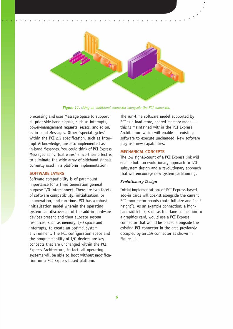
Evolutionary Design
Initial implementations of PCI Express-based
add-in cards will coexist alongside the current
PCI-form factor boards (both full size and “half-
height”). As an example connection; a high-
bandwidth link, such as four-lane connection to
a graphics card, would use a PCI Express
connector that would be placed alongside the
existing PCI connector in the area previously
occupied by an ISA connector as shown in
Figure 11.
Figure 11. Using an additional connector alongside the PCI connector.
8/11/2019 Pci Express Intel
http://slidepdf.com/reader/full/pci-express-intel 7/8
7
Microphone
Camera
Speaker
CD Player
USB
Figure 12. PCI Express™ enables revolutionary platform form factors.
Figure 13. A small form factor concept for mobile applications.
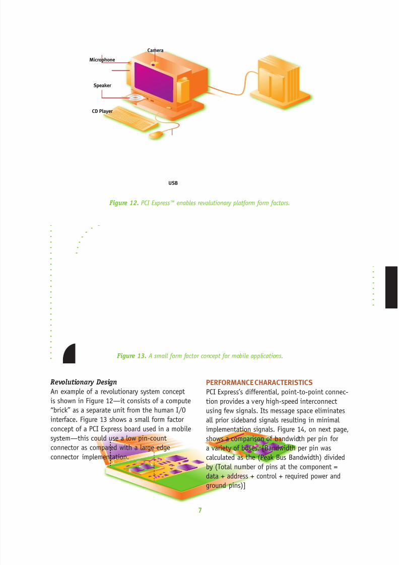
Revolutionary Design
An example of a revolutionary system concept
is shown in Figure 12—it consists of a compute
“brick” as a separate unit from the human I/O
interface. Figure 13 shows a small form factor
concept of a PCI Express board used in a mobile
system—this could use a low pin-count
connector as compared with a large edge
connector implementation.
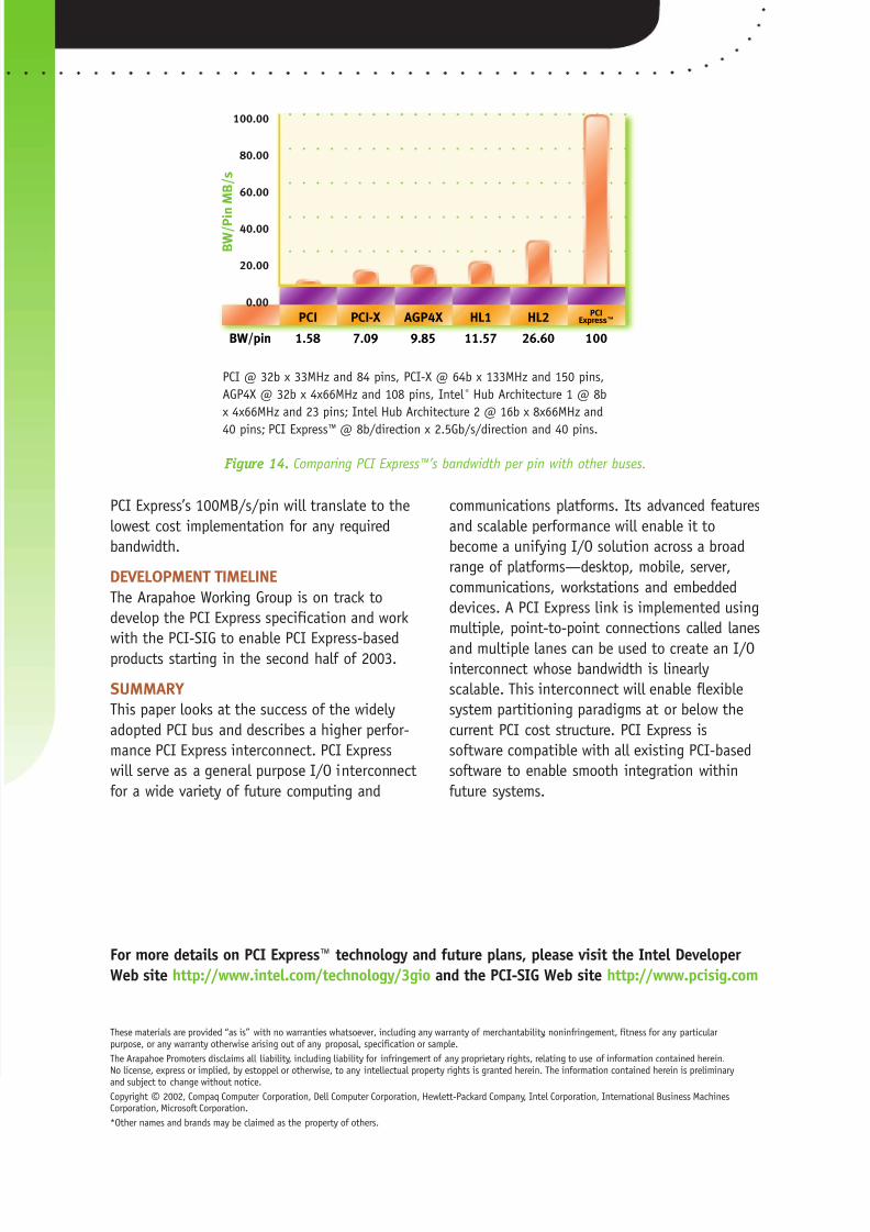
PERFORMANCE CHARACTERISTICS
PCI Express’s differential, point-to-point connec-
tion provides a very high-speed interconnect
using few signals. Its message space eliminates
all prior sideband signals resulting in minimal
implementation signals. Figure 14, on next page,
shows a comparison of bandwidth per pin for
a variety of buses. [Bandwidth per pin was
calculated as the (Peak Bus Bandwidth) divided
by (Total number of pins at the component =
data + address + control + required power and
ground pins)]
8/11/2019 Pci Express Intel
http://slidepdf.com/reader/full/pci-express-intel 8/8
For more details on PCI Express™ technology and future plans, please visit the Intel Developer
Web site http://www.intel.com/technology/3gio and the PCI-SIG Web site http://www.pcisig.com
PCI Express’s 100MB/s/pin will translate to the
lowest cost implementation for any required
bandwidth.
DEVELOPMENT TIMELINE
The Arapahoe Working Group is on track to
develop the PCI Express specification and work
with the PCI-SIG to enable PCI Express-based
products starting in the second half of 2003.
SUMMARY
This paper looks at the success of the widely
adopted PCI bus and describes a higher perfor-
mance PCI Express interconnect. PCI Express
will serve as a general purpose I/O interconnect
for a wide variety of future computing and
communications platforms. Its advanced features
and scalable performance will enable it to
become a unifying I/O solution across a broad
range of platforms—desktop, mobile, server,
communications, workstations and embedded
devices. A PCI Express link is implemented using
multiple, point-to-point connections called lanes
and multiple lanes can be used to create an I/Ointerconnect whose bandwidth is linearly
scalable. This interconnect will enable flexible
system partitioning paradigms at or below the
current PCI cost structure. PCI Express is
software compatible with all existing PCI-based
software to enable smooth integration within
future systems.
B W / P i n M B / s
PCI
1.58BW/pin
PCI-X
7.09
AGP4X
9.85
HL1
11.57
HL2
26.60
PCIExpress™
100
100.00
80.00
60.00
40.00
20.00
0.00
Figure 14. Comparing PCI Express™’s bandwidth per pin with other buses.
PCI @ 32b x 33MHz and 84 pins, PCI-X @ 64b x 133MHz and 150 pins,
AGP4X @ 32b x 4x66MHz and 108 pins, Intel ® Hub Architecture 1 @ 8b
x 4x66MHz and 23 pins; Intel Hub Architecture 2 @ 16b x 8x66MHz and
40 pins; PCI Express™ @ 8b/direction x 2.5Gb/s/direction and 40 pins.
These materials are provided “as is” with no warranties whatsoever, including any warranty of merchantability, noninfringement, fitness for any particularpurpose, or any warranty otherwise arising out of any proposal, specification or sample.
The Arapahoe Promoters disclaims all liability, including liability for infringement of any proprietary rights, relating to use of information contained herein.No license, express or implied, by estoppel or otherwise, to any intellectual property rights is granted herein. The information contained herein is preliminary
and subject to change without notice.
Copyright © 2002, Compaq Computer Corporation, Dell Computer Corporation, Hewlett-Packard Company, Intel Corporation, International Business MachinesCorporation, Microsoft Corporation.
*Other names and brands may be claimed as the property of others.