PCI Express Compiler v6.1 User Guide
256
101 Innovation Drive San Jose, CA 95134 (408) 544-7000 www.altera.com PCI Express Compiler User Guide MegaCore Version: 6.1 Document Version: 6.1 rev. 2 Document Date: December 2006
Transcript of PCI Express Compiler v6.1 User Guide

101 Innovation DriveSan Jose, CA 95134(408) 544-7000www.altera.com
PCI Express Compiler
User Guide
MegaCore Version: 6.1Document Version: 6.1 rev. 2Document Date: December 2006

Copyright © 2006 Altera Corporation. All rights reserved. Altera, The Programmable Solutions Company, the stylized Altera logo, specific device des-ignations, and all other words and logos that are identified as trademarks and/or service marks are, unless noted otherwise, the trademarks andservice marks of Altera Corporation in the U.S. and other countries. All other product or service names are the property of their respective holders. Al-tera products are protected under numerous U.S. and foreign patents and pending applications, maskwork rights, and copyrights. Altera warrantsperformance of its semiconductor products to current specifications in accordance with Altera's standard warranty, but reserves the right to makechanges to any products and services at any time without notice. Altera assumes no responsibility or liability arising out of the ap-plication or use of any information, product, or service described herein except as expressly agreed to in writing by AlteraCorporation. Altera customers are advised to obtain the latest version of device specifications before relying on any published in-formation and before placing orders for products or services.
ii PCI Express Compiler Version 6.1 Altera CorporationPCI Express Compiler User Guide User Guide
UG-PCI10605-1.4.1

Altera Corporation PCI ExDecember 2006
Contents
About This User GuideRevision History ....................................................................................................................................... ixHow to Contact Altera ............................................................................................................................. xiTypographic Conventions ..................................................................................................................... xii
Chapter 1. About This CompilerRelease Information ............................................................................................................................... 1–1Device Family Support ......................................................................................................................... 1–1New in PCI Express Compiler Version 6.1 ........................................................................................ 1–2Features ................................................................................................................................................... 1–2General Description ............................................................................................................................... 1–3
Testbench & Example Designs: Simple DMA and Chaining DMA .......................................... 1–5OpenCore Plus Evaluation .............................................................................................................. 1–6
Performance ............................................................................................................................................ 1–7
Chapter 2. Getting StartedDesign Flow ............................................................................................................................................ 2–1PCI Express Walkthrough .................................................................................................................... 2–2
Launch the MegaWizard Plug-In Manager .................................................................................. 2–3Parameterize ..................................................................................................................................... 2–5Set Up Simulation ............................................................................................................................. 2–9Generate Files .................................................................................................................................. 2–11
Simulate the Design ............................................................................................................................. 2–14IP Functional Simulation Model .................................................................................................. 2–14
Compile the Design ............................................................................................................................. 2–15Program a Device ................................................................................................................................ 2–16Set Up Licensing .................................................................................................................................. 2–16
press Compiler Version 6.1 iii

Contents
Chapter 3. SpecificationsFunctional Description .......................................................................................................................... 3–1
Endpoint Types ................................................................................................................................ 3–2Transaction Layer ............................................................................................................................. 3–2Data Link Layer ................................................................................................................................ 3–7Physical Layer ................................................................................................................................. 3–10Analyzing Throughput .................................................................................................................. 3–11Configuration Space Register Content ........................................................................................ 3–18Active State Power Management (ASPM) .................................................................................. 3–22Error Handling ............................................................................................................................... 3–24Stratix GX PCI Express Compatibility ........................................................................................ 3–29OpenCore Plus Time-Out Behavior ............................................................................................. 3–30
Parameter Settings ............................................................................................................................... 3–31System Settings Page ..................................................................................................................... 3–31Capabilities Page Parameters ....................................................................................................... 3–35Buffer Setup Page ........................................................................................................................... 3–37Power Management Page ............................................................................................................. 3–41
Signals ................................................................................................................................................... 3–43Transmit Interface Operation Signals .......................................................................................... 3–45Receive Interface Operation Signals ............................................................................................ 3–61Clocking ........................................................................................................................................... 3–72Utility Signals .................................................................................................................................. 3–78alt2gxb Support Signals ................................................................................................................. 3–89Physical Layer Interface Signals ................................................................................................... 3–90
MegaCore Verification ........................................................................................................................ 3–94Simulation Environment ............................................................................................................... 3–94Compatibility Testing Environment ............................................................................................ 3–94
Chapter 4. External PHYsExternal PHY Support ........................................................................................................................... 4–1
16-bit SDR Mode ............................................................................................................................... 4–216-bit SDR Mode with a Source Synchronous TxClk .................................................................. 4–38-bit DDR Mode ................................................................................................................................ 4–58-bit DDR with a Source Synchronous TxClk .............................................................................. 4–68-bit SDR Mode ................................................................................................................................. 4–88-bit SDR with a Source Synchronous TxClk ............................................................................... 4–916-bit PHY Interface Signals ......................................................................................................... 4–118-bit PHY Interface Signals ........................................................................................................... 4–13
Selecting an External PHY .................................................................................................................. 4–15External PHY Constraint Support ..................................................................................................... 4–16
Using External PHYs With the Stratix GX Device Family ....................................................... 4–17
iv PCI Express Compiler Version 6.1 Altera CorporationPCI Express Compiler User Guide December 2006

Contents
Chapter 5. Testbench & Example DesignsTestbench ................................................................................................................................................ 5–3Simple DMA Example Design ............................................................................................................. 5–5
Example Design BAR/Address Map ............................................................................................ 5–8Chaining DMA Example Design ....................................................................................................... 5–11
Example Design BAR/Address Map .......................................................................................... 5–16Chaining DMA Descriptor Tables ............................................................................................... 5–17
Test Driver Modules ............................................................................................................................ 5–20BFM Test Driver Module For Simple DMA Example Design ................................................. 5–20BFM Test Driver Module for Chaining DMA Example Design .............................................. 5–23
Root Port BFM ...................................................................................................................................... 5–27BFM Memory Map ......................................................................................................................... 5–29Configuration Space Bus and Device Numbering .................................................................... 5–29Configuration of Root Port and Endpoint .................................................................................. 5–30Issuing Read & Write Transactions to the Application Layer ................................................. 5–32
BFM Procedures and Functions ......................................................................................................... 5–33BFM Read and Write Procedures ................................................................................................. 5–34BFM Performance Counting ......................................................................................................... 5–41BFM Read/Write Request Procedures ........................................................................................ 5–42BFM Configuration Procedures ................................................................................................... 5–44BFM Shared Memory Access Procedures ................................................................................... 5–46BFM Log & Message Procedures ................................................................................................. 5–50Verilog HDL Formatting Functions ............................................................................................. 5–56Procedures and Functions Specific to the chaining DMA Design .......................................... 5–61
Appendix A. Configuration Signals
Configuration Signals for x1 and x4 MegaCore Functions ............................................................. A–1Configuration Signals for x8 MegaCore Functions ......................................................................... A–6
Appendix B. Transaction Layer Packet Header Formats
Content Without Data Payload .......................................................................................................... B–1Content with Data Payload ................................................................................................................. B–2
Appendix C. Test Port Interface Signals
Test-Out Interface Signals for x1 and x4 MegaCore Functions .......................................................................................................... C–2Test-Out Interface Signals for x8 MegaCore Functions ................................................................ C–19Test-In Interface .................................................................................................................................. C–22
Altera Corporation PCI Express Compiler Version 6.1 vDecember 2006 PCI Express Compiler User Guide

Contents
vi PCI Express Compiler Version 6.1 Altera CorporationPCI Express Compiler User Guide December 2006

About This User Guide
About This User Guide
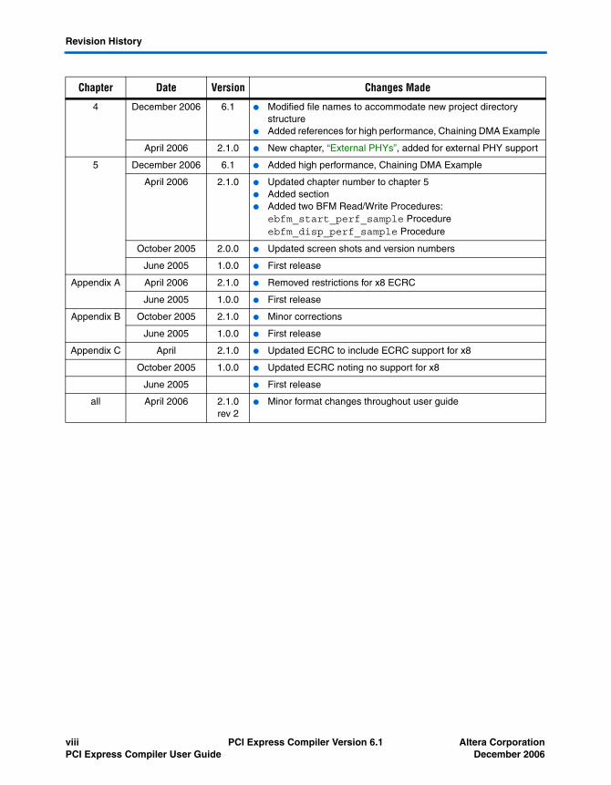
Revision History The table below displays the revision history for the chapters in this User Guide.
Chapter Date Version Changes Made
1 December 2006 6.1 ● Added support for the Stratix® III device family ● Updated version and performance information
April 2006 2.1.0 ● Rearranged content● Updated performance information
October 2005 2.0.0 ● Added x8 support● Added device support for Stratix II GX and Cyclone® II ● Updated performance information
June 2005 1.0.0 ● First release
2 December 6.1 ● Updated screen shots and version numbers ● Modified text to accommodate new MegaWizard® interface ● Updated installation diagram● Updated walkthrough to accommodate new MegaWizard
interface
April 2006 2.1.0 ● Updated screen shots and version numbers ● Added steps for sourcing Tcl constraint file during compilation to
the walkthrough in the section “Compile the Design” on page 2–15
● Moved installation information to release notes
October 2005 2.0.0 ● Updated screen shots and version numbers
June 2005 1.0.0 ● First release
3 December 2006 6.1 ● Updated screen shots and parameters for new MegaWizard interface
● Corrected timing diagrams
April 2006 2.1.0 ● Added section “Analyzing Throughput” on page 3–11● Updated screen shots and version numbers● Updated System Settings, Capabilities, Buffer Setup, and Power
Management Pages and their parameters● Added three waveform diagrams:
Transfer for a single writeTransaction layer not ready to accept packetTransfer with wait state inserted for a single DWORD
October 2005 2.0.0 ● Updated screen shots and version numbers
June 2005 1.0.0 ● First release
Altera Corporation PCI Express Compiler Version 6.1 viiDecember 2006 PCI Express Compiler User Guide
Revision History
4 December 2006 6.1 ● Modified file names to accommodate new project directory structure
● Added references for high performance, Chaining DMA Example
April 2006 2.1.0 ● New chapter, “External PHYs”, added for external PHY support
5 December 2006 6.1 ● Added high performance, Chaining DMA Example
April 2006 2.1.0 ● Updated chapter number to chapter 5● Added section ● Added two BFM Read/Write Procedures:
ebfm_start_perf_sample Procedureebfm_disp_perf_sample Procedure
October 2005 2.0.0 ● Updated screen shots and version numbers
June 2005 1.0.0 ● First release
Appendix A April 2006 2.1.0 ● Removed restrictions for x8 ECRC
June 2005 1.0.0 ● First release
Appendix B October 2005 2.1.0 ● Minor corrections
June 2005 1.0.0 ● First release
Appendix C April 2.1.0 ● Updated ECRC to include ECRC support for x8
October 2005 1.0.0 ● Updated ECRC noting no support for x8
June 2005 ● First release
all April 2006 2.1.0 rev 2
● Minor format changes throughout user guide
Chapter Date Version Changes Made
viii PCI Express Compiler Version 6.1 Altera CorporationPCI Express Compiler User Guide December 2006

About This User Guide
How to Contact Altera
For the most up-to-date information about Altera® products, go to the Altera website at www.altera.com. For technical support on this product, go to www.altera.com/mysupport. For additional information about Altera products, consult the sources shown below.
Information Type USA & Canada All Other Locations
Technical support www.altera.com/mysupport/ www.altera.com/mysupport/
(800) 800-EPLD (3753)(7:00 a.m. to 5:00 p.m. Pacific Time)
+1 408-544-87677:00 a.m. to 5:00 p.m. (GMT -8:00) Pacific Time
Product literature www.altera.com www.altera.com
Altera literature services [email protected] [email protected]
Nontechnical customer service
(800) 767-3753 + 1 408-544-70007:00 a.m. to 5:00 p.m. (GMT -8:00) Pacific Time
FTP site ftp.altera.com ftp.altera.com
Altera Corporation PCI Express Compiler Version 6.1 ixDecember 2006 PCI Express Compiler User Guide

Typographic Conventions
Typographic Conventions
This document uses the typographic conventions shown below.
Visual Cue Meaning
Bold Type with Initial Capital Letters
Command names, dialog box titles, checkbox options, and dialog box options are shown in bold, initial capital letters. Example: Save As dialog box.
bold type External timing parameters, directory names, project names, disk drive names, filenames, filename extensions, and software utility names are shown in bold type. Examples: fMAX, \qdesigns directory, d: drive, chiptrip.gdf file.
Italic Type with Initial Capital Letters
Document titles are shown in italic type with initial capital letters. Example: AN 75: High-Speed Board Design.
Italic type Internal timing parameters and variables are shown in italic type. Examples: tPIA, n + 1.
Variable names are enclosed in angle brackets (< >) and shown in italic type. Example: <file name>, <project name>.pof file.
Initial Capital Letters Keyboard keys and menu names are shown with initial capital letters. Examples: Delete key, the Options menu.
“Subheading Title” References to sections within a document and titles of on-line help topics are shown in quotation marks. Example: “Typographic Conventions.”
Courier type Signal and port names are shown in lowercase Courier type. Examples: data1, tdi, input. Active-low signals are denoted by suffix n, e.g., resetn.
Anything that must be typed exactly as it appears is shown in Courier type. For example: c:\qdesigns\tutorial\chiptrip.gdf. Also, sections of an actual file, such as a Report File, references to parts of files (for example, the VHDL keyword BEGIN), as well as logic function names (for example, TRI) are shown in Courier.
1., 2., 3., anda., b., c., etc.
Numbered steps are used in a list of items when the sequence of the items is important, such as the steps listed in a procedure.
■ ● • Bullets are used in a list of items when the sequence of the items is not important.
v The checkmark indicates a procedure that consists of one step only.
1 The hand points to information that requires special attention.
cA caution calls attention to a condition or possible situation that can damage or destroy the product or the user’s work.
w A warning calls attention to a condition or possible situation that can cause injury to the user.
r The angled arrow indicates you should press the Enter key.
f The feet direct you to more information on a particular topic.
x PCI Express Compiler Version 6.1 Altera CorporationPCI Express Compiler User Guide December 2006

Altera Corporation PCI ExpDecember 2006
1. About This Compiler
Release Information
Table 1–1 provides information about this release of the Altera® PCI Express Compiler.
Device Family Support
MegaCore® functions provide either full or preliminary support for target Altera device families:
■ Full support means the MegaCore function meets all functional and timing requirements for the device family and may be used in production designs
■ Preliminary support means the MegaCore function meets all functional requirements, but may still be undergoing timing analysis for the device family; it may be used in production designs with caution.
Table 1–1. PCI Express Compiler Release Information
Item Description
Version 6.1
Release Date December 2006
Ordering Code IP-PCIE/1IP-PCIE/4IP-PCIE/8
Product IDs 00A900AA00AB
Vendor ID 6A66
ress Compiler Version 6.1 1–1Preliminary
New in PCI Express Compiler Version 6.1
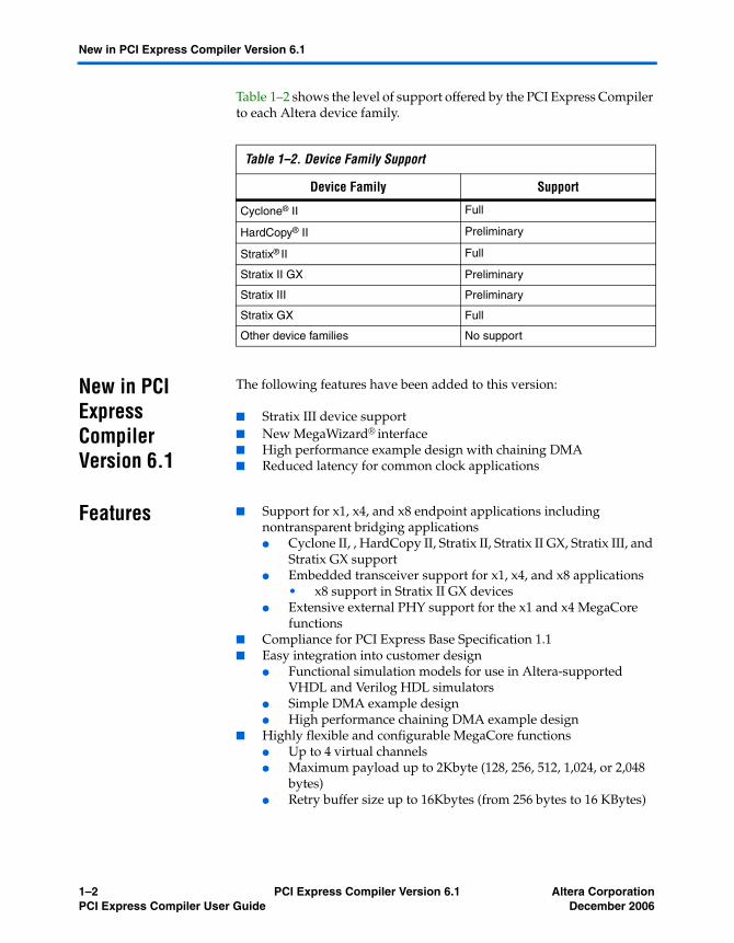
Table 1–2 shows the level of support offered by the PCI Express Compiler to each Altera device family.
New in PCI Express Compiler Version 6.1
The following features have been added to this version:
■ Stratix III device support■ New MegaWizard® interface■ High performance example design with chaining DMA ■ Reduced latency for common clock applications
Features ■ Support for x1, x4, and x8 endpoint applications including nontransparent bridging applications● Cyclone II, , HardCopy II, Stratix II, Stratix II GX, Stratix III, and
Stratix GX support● Embedded transceiver support for x1, x4, and x8 applications
• x8 support in Stratix II GX devices● Extensive external PHY support for the x1 and x4 MegaCore
functions■ Compliance for PCI Express Base Specification 1.1■ Easy integration into customer design
● Functional simulation models for use in Altera-supported VHDL and Verilog HDL simulators
● Simple DMA example design● High performance chaining DMA example design
■ Highly flexible and configurable MegaCore functions● Up to 4 virtual channels● Maximum payload up to 2Kbyte (128, 256, 512, 1,024, or 2,048
bytes)● Retry buffer size up to 16Kbytes (from 256 bytes to 16 KBytes)
Table 1–2. Device Family Support
Device Family Support
Cyclone® II Full
HardCopy® II Preliminary
Stratix® II Full
Stratix II GX Preliminary
Stratix III Preliminary
Stratix GX Full
Other device families No support
1–2 PCI Express Compiler Version 6.1 Altera CorporationPCI Express Compiler User Guide December 2006

About This Compiler
■ Access to high reliability features● Optional end-to-end cyclic redundancy code (ECRC)/advanced
error reporting (AER) support for x1, x4, and x8 lanes■ Free evaluation using OpenCore Plus
General Description
The PCI Express Compiler generates customized PCI Express MegaCore functions you use to design PCI Express endpoints, including non-transparent bridges, or truly unique designs combining multiple PCI Express components in a single Altera device. The PCI Express MegaCore functions are PCI Express Base Specification Revision 1.1 or PCI Express™ Base Specification Revision 1.0a compliant, and implement all required and most optional features of the specification for the transaction, data link, and physical layers.
The PCI Express Compiler allows you to select from 3 MegaCore functions that support x1, x4, or x8 operation and that are suitable for endpoint applications. Figure 1–1 shows how the PCI Express MegaCore functions can be used in an example system. If you target the MegaCore function for Stratix GX or Stratix II GX devices, the MegaCore function includes a complete PHY layer, including the MAC, PCS, and PMA layers. If you target other device architectures, the PCI Express Compiler generates the MegaCore function with the Intel-designed PIPE interface, making the MegaCore function usable with other PIPE-compliant external PHY devices.
When selecting your external PHY, the PCI Express MegaCore functions support a wide range of PHYs including the TI XIO1100 PHY in 8-bit DDR mode or 16-bit SDR mode; Philips PX1011A for 8-bit SDR mode, a serial PHY for Stratix II GX and Stratix GX devices, and a range of custom PHYs using 8-bit/16-bit SDR with or without source synchronous transmit cock modes and 8-bit DDR with or without source synchronous transmit clock modes.
Altera Corporation PCI Express Compiler Version 6.1 1–3December 2006 PCI Express Compiler User Guide

General Description
Figure 1–1. Example PCI Express System
Optimized for Altera devices, the PCI Express Compiler supports all memory, I/O, configuration, and message transactions. The MegaCore functions have a highly optimized application interface to achieve maximum effective throughput. Because the Compiler is parameterizable, you can customize them to meet design requirements by using the MegaWizard interface in the Quartus® II software. For example, the MegaCore functions can support up to 4 virtual channels for x1 or x4 configurations, or up to 2 channels for x8 configurations. You also can customize the payload size, buffer sizes, and configuration space (base address registers support and other registers). Additionally, the PCI Express Compiler supports end-to-end cyclic redundancy code (ECRC) and advanced error reporting for x1, x4, and x8 configurations.
The PCI Express MegaCore functions also include debug features that allow observation and control of the MegaCore functions. These additional inputs and outputs help with faster debugging of system-level problems.
RootComplex
Switch
Stratix GX or Stratix II GX Device
User Application Logic
PCI ExpressMegaCore Function
Endpoint
Stratix II or Cyclone II Device
User Application Logic
PCI ExpressMegaCore Function
Endpoint
PIPE Interface
PCI Express Link
External PHY
PCI Express Link
1–4 PCI Express Compiler Version 6.1 Altera CorporationPCI Express Compiler User Guide December 2006

About This Compiler
Testbench & Example Designs: Simple DMA and Chaining DMA
The PCI Express Compiler includes an endpoint testbench that incorporates a basic root port bus functional model (BFM) and two endpoint design examples: simple DMA and chaining DMA. Both endpoint design examples illustrate the application interface to the PCI Express MegaCore function and are delivered as clear-text source-code (VHDL and Verilog HDL) suitable for both simulation and synthesis, as well as OpenCore Plus evaluation of the MegaCore function in hardware. The basic root port BFM incorporates a driver and an IP functional simulation model of a root port. Figure 1–2 illustrates the endpoint testbench setup for the simple DMA example. Figure 1–3 illustrates the testbench for the chaining DMA example.
Figure 1–2. Testbench for the Simple DMA Example
Endpoint Simple DMA Example
Root Port Driver
x8 Root Port Model
User Interface
Root Port BFM
TargetControl
PCI ExpressMegaCore Function
Endpoint Application Layer Example
DMAControl
Registers
DMAControl
TargetMemory
(32 KBytes)
DMAMemory
(32 KBytes)
Traffic Control/Virtual Channel MappingRequest/Completion Routing
User Interface
PCI Express Link
Altera Corporation PCI Express Compiler Version 6.1 1–5December 2006 PCI Express Compiler User Guide

General Description
You can replace the endpoint application layer example shown in Figure 1–2 or Figure 1–3 with your own application layer design and then modify the BFM driver to generate the transactions needed to test your application layer.
Figure 1–3. Testbench for the Chaining DMA Example
OpenCore Plus Evaluation
With Altera’s free OpenCore Plus evaluation feature, you can perform the following actions:
■ Simulate the behavior of a MegaCore function within your system■ Verify the functionality of your design, as well as quickly and easily
evaluate its size and speed
Endpoint Example
Root Port Driver
x8 Root Port Model
User Interface
Root Port BFM
PCI ExpressMegaCore Function
Endpoint Application Layer Example
DMAWrite
RCSlave
(Optional)
Endpoint Memory
(32 KBytes)
Traffic Control/Virtual Channel MappingRequest/Completion Routing
User Interface
PCI Express Link
DMARead
1–6 PCI Express Compiler Version 6.1 Altera CorporationPCI Express Compiler User Guide December 2006

About This Compiler
■ Generate time-limited device programming files for designs that include MegaCore functions
■ Program a device and verify your design in hardware
You only need to purchase a license for the MegaCore function when you are completely satisfied with its functionality and performance, and want to take your design to production.
f For more information on OpenCore Plus hardware evaluation using the PCI Express compiler, see “OpenCore Plus Time-Out Behavior” on page 3–30 and AN 320: OpenCore Plus Evaluation of Megafunctions.
Performance Tables in this section show typical expected performance for various parameters using the Quartus II software, version 6.1 for the device families listed.
For the performance data in Table 1–3 through Table 1–7, the parameters below were set.
■ On the Buffer Setup page, for x1, x4, and x8 configurations, the following values were set:● Maximum payload size was set to 256 Bytes unless specified
otherwise.● Desired performance for received requests and Desired
performance for completions were both set to Medium. unless otherwise specified.
1 For a description of the Buffer Setup page settings, see Table 3–20 on page 3–38.
■ On the Capabilities page, the number of Tags supported was set as to 16 for all configurations unless specified otherwise.
1 For a description of Capabilities page settings, see Table 3–19 on page 3–35.
Altera Corporation PCI Express Compiler Version 6.1 1–7December 2006 PCI Express Compiler User Guide

Performance
Table 1–3 shows the typical expected performance for different parameters, using the Quartus II software, version 6.1 for Cyclone II (EP2C35F484C6) devices.
Table 1–3. Performance - Cyclone II Devices
Parameters Memory Blocks
x1/x4 InternalClock MHz
Number of Virtual
Channels
Logic Elements M4K
x1 125 1 9500 10
x1 125 2 12400 15
x1(1) 62.5 1 7800 11
x1 62.5 2 10500 18
x4 125 1 12100 18
x4 125 2 15200 27
Notes for Table 1–3(1) Max payload was set to 128B, the number of Tags supported was set to 4, and Desired
performance for received requests and Desired performance for completions were both set to Low.
1–8 PCI Express Compiler Version 6.1 Altera CorporationPCI Express Compiler User Guide December 2006

About This Compiler
6.1 Table 1–4 shows the typical expected performance for different parameters, using the Quartus II software, version 6.1 for Stratix II (EP2S130GF1508C3) devices.
Table 1–4. Performance - Stratix II Devices
Parameters Memory Blocks
x1/x4InternalClock MHz
Number of Virtual
Channels
Combinational ALUTs
DedicatedRegisters M512 M4K
x1 125 1 6600 3400 2 8
x1 125 2 8900 4500 3 12
x4 125 1 8700 4400 6 12
x4 125 2 11000 5600 7 20
Altera Corporation PCI Express Compiler Version 6.1 1–9December 2006 PCI Express Compiler User Guide

Performance
Table 1–5 shows the typical expected performance for different parameters, using the Quartus II software version 6.1 for Stratix II GX (EP2SGX130GF1508C3) devices.
Table 1–5. Performance - Stratix II GX Devices
Parameters Memory Blocks
x1/x4/x8InternalClock MHz
Number of Virtual
Channels
Combinational ALUTs
DedicatedRegisters M512 M4K
x1 125 1 6600 3400 2 8
x1 125 2 8900 4500 3 12
x4 125 1 8700 4400 6 12
x4 125 2 11000 5600 7 20
x8 250 1 8300 5800 10 12
x8 250 2 10200 6900 11 20
1–10 PCI Express Compiler Version 6.1 Altera CorporationPCI Express Compiler User Guide December 2006

About This Compiler
Table 1–6 shows the typical expected performance for different parameters, using the Quartus II software version 6.1 for Stratix III (EP3SL200F1152C3) devices.
Table 1–7 shows the typical expected performance for different parameters, using the Quartus II software version 6.1 for Stratix GX (EP1SGX25CF672C5) devices.
Table 1–6. Performance - Stratix III Devices
Parameters Memory Blocks
x1/x4InternalClock MHz
Max Payload
Bytes
Number of VirtualChannels
Combinational ALUTs
DedicatedRegisters M9K
x1 125 256 1 6500 3400 5
x1 125 256 2 8700 4500 9
x4 125 256 1 8500 4500 7
x4 125 256 2 10900 5600 12
Table 1–7. Performance - Stratix GX
Parameters Memory Blocks
x1/x4 InternalClock MHz
Number of Virtual
Channels
LogicElements M512 M4K
x1 125 1 9500 2 9
x1 125 2 12300 2 14
x4 125 1 14500 6 16
x4 125 2 17100 7 24
Altera Corporation PCI Express Compiler Version 6.1 1–11December 2006 PCI Express Compiler User Guide

Performance
The following table shows the recommended device family speed grades for the supported link widths and internal clock frequencies. When the internal clock frequency is 125 MHz or 250 MHz, the recommended setting is that the Quartus II Analysis & Synthesis Optimization Technique be set to Speed.
f See the Quartus II Development Software Handbook for more information on how to set this.
Table 1–8. Recommended Device Family and Speed Grades
Device Family Link Width Internal Clock Frequency
Recommended Speed Grades
Cyclone II x1, x4 125MHz -6
x1 62.5MHz -6, -7, -8(4)
Stratix II GX x1, x4 125MHz -3, -4, -5 (1)
x8 250MHz -3(1), -4(2),(3)
Stratix II x1, x4 125MHz -3, -4, -5 (1)
x1 62.5Mhz -3, -4, -5
Stratix III x1, x4 125MHz -2,-3,-4
x1 62.5MHz -2,-3,-4
Stratix GX x1, x4 125MHz -5(1)
x1 62.5MHz -5,-6
Notes:(1) To achieve timing closure for these speed grades and variations enabling Physical Synthesis
in the Quartus II Fitter Settings is required with these options enabled: Perform physical synthesis for combinational logic, perform register duplication, and perform register retiming. See the Quartus II Development Software Handbook for more information on how to set these options.
(2) Achieving timing closure for x8 in Stratix II GX -4 will require use of the Quartus Design Space Explorer with multiple seeds.
(3) Multiple VCs, ECRC support, and greater than 16 tags are not recommended for x8 variations in Stratix II GX -4.
(4) In the -8 speed grade, the External PHY 16-bit SDR or 8-bit SDR modes are recommended
1–12 PCI Express Compiler Version 6.1 Altera CorporationPCI Express Compiler User Guide December 2006

Altera Corporation PCI ExDecember 2006
2. Getting Started
Design Flow To evaluate the PCI Express Compiler using the OpenCore Plus feature include these steps in your design flow:
1. Obtain and install the PCI Express Compiler.
The PCI Express Compiler is part of the MegaCore® IP Library, which is distributed with the Quartus II software and downloadable from the Altera website, www.altera.com.
For system requirements and installation instructions, refer to Quartus II Installation & Licensing for Windows or Quartus II Installation & Licensing for UNIX & Linux on the Altera website at
www.altera.com/literature/lit-qts.jsp
Figure 2–1 shows the directory structure after you install the PCI Express Compiler, where <path> is the installation directory. The default installation directory on Windows is c:\altera\61; on UNIX and Linux it is /opt/altera/61.
Figure 2–1. Directory Structure
commonContains shared components.
pci_express_compilerContains the PCI Express Compiler files and documentation.
doc Contains documentation for the MegaCore function.
lib Contains encrypted lower-level design files and other support files.
<path>Installation directory
ip Contains the MegaCore IP Library
press Compiler Version 6.1 2–1Preliminary

PCI Express Walkthrough
2. Create a custom variation using the PCI Express Compiler.
3. Implement the rest of your design using the design entry method of your choice.
4. Use the IP functional simulation model to verify the operation of your design.
f For more information on IP functional simulation models, refer to the Simulating Altera IP in Third-Party Simulation Tools chapter in volume 3 of the Quartus II Development Software Handbook.
5. Use the Quartus II software to compile your design.
1 You can also generate an OpenCore Plus time-limited programming file, which you can use to verify the operation of your design in hardware.
6. Purchase a license for the PCI Express Compiler.
After you have purchased a license for the PCI Express Compiler Compiler, follow these additional steps:
1. Set up licensing.
2. Generate a programming file for the Altera® device(s) on your board.
3. Program the Altera device(s) with the completed design.
PCI Express Walkthrough
The PCI Express Compiler comes with 2 example designs. This walkthrough guides you through the process of launching the MegaWizard interface using the MegaWizard Plug-in Manager, parameterizing the MegaCore, and simulating the MegaCore with your choice of the 2 supplied example designs. After generating a custom variation of the PCI Express MegaCore function, you can incorporate it into your overall project.
This walkthrough consists of the following steps:
■ Launch the MegaWizard Plug-In Manager■ Parameterize■ Set Up Simulation■ Generate Files
2–2 PCI Express Compiler Version 6.1 Altera CorporationPCI Express Compiler User Guide December 2006

Getting Started
The PCI Express Compiler MegaWizard interface creates two example top-level designs to connect with the PCI Express MegaCore function variation that you create. The example top-level designs can be compiled for an Altera device by the Quartus II software. The example simple DMA top-level design is named <variation name>_example_top. This walkthrough uses pex as the variation name and pex_example_top as the simple DMA top-level example design.
The example chaining DMA top-level design is named pex_example_chaining_top.
Launch the MegaWizard Plug-In Manager
To launch the MegaWizard® Plug-In Manager in the Quartus II software, follow these steps:
1. Start the MegaWizard Plug-In Manager by choosing MegaWizard Plug-In Manager (Tools menu). The MegaWizard Plug-In Manager dialog box displays (see Figure 2–2).
1 Refer to the Quartus II Help for more information on how to use the MegaWizard Plug-In Manager.
Figure 2–2. MegaWizard Plug-In Manager
2. Specify that you want to create a new custom megafunction variation and click Next.
Altera Corporation PCI Express Compiler Version 6.1 2–3December 2006 PCI Express Compiler User Guide

PCI Express Walkthrough
3. Expand the Interfaces directory under Installed Plug-Ins by clicking the + icon left of the directory name, then click PCI Express Compiler v6.1.
4. Choose the device family you want to use for this MegaCore function variation. For example, Stratix II GX.
5. Select the output file type for your design; the MegaWizard Plug-In Manager supports VHDL and Verilog HDL. In this example, choose Verilog HDL.
6. The MegaWizard Plug-In Manager shows the project path that you specified. Append a variation name for the MegaCore function output files <project path>\<variation name>. For this walkthrough, specify pex for the name of the MegaCore function files:
c:\altera\pcie_project\pex.vhd
Figure 2–3 shows the MegaWizard Plug-In Manager after you have made these settings.
Figure 2–3. Select the MegaCore Function
2–4 PCI Express Compiler Version 6.1 Altera CorporationPCI Express Compiler User Guide December 2006

Getting Started
7. Click Next to display the Parameter Settings page for the PCI Express Compiler (see Figure 2–4).
1 You can change the page that the MegaWizard Plug-In Manager displays by clicking Next or Back at the bottom of the dialog box. You can move directly to a named page by clicking Parameter Settings, Simulation Model, or Summary tab.
Also, you can directly display individual parameter settings by clicking on options on specific parameter pages.
Parameterize
To parameterize your MegaCore function, follow these steps:
1 For this section, you can use the parameter settings shown in the figures or your own settings. The example design is generated to adapt to most settings, although some tests may not run for specific settings. The parameter settings required to use the testbench fully are noted for each MegaWizard page.
1. Click the Parameter Settings tab in the MegaWizard interface (see Figure 2–4).
The System Settings page is the first page displayed. Set parameters on this page that are appropriate for the MegaCore function instance you will implement. See Figure 2–4.
Altera Corporation PCI Express Compiler Version 6.1 2–5December 2006 PCI Express Compiler User Guide

PCI Express Walkthrough
Figure 2–4. System Settings Page
To enable all of the tests in the provided testbench and Simple DMA example design, make the BAR assignments shown in Table 2–1 below.
1 Many other BAR settings allow full testing of the Simple DMA example design. See the “BFM Test Driver Module For Simple DMA Example Design” on page 5–20 for a description of what settings the test module uses.
Table 2–1. BAR Assignments
BAR BAR TYPE BAR Size
1:0 64-Bit Prefetchable Memory 16 MBytes - 24 bits
2 32-bit Non-Prefetchable Memory 256 Kbytes -18 bits
2–6 PCI Express Compiler Version 6.1 Altera CorporationPCI Express Compiler User Guide December 2006

Getting Started
See “Parameter Settings” on page 3–31 for a detailed description of the available parameters.
2. Click Next to display the Capabilities page.
3. With the Capabilities page open, make the appropriate settings and click Next to display the Buffer Setup page. See Figure 2–5.
Figure 2–5. Capabilities Page
Altera Corporation PCI Express Compiler Version 6.1 2–7December 2006 PCI Express Compiler User Guide

PCI Express Walkthrough
4. The Buffer Setup page opens. Make the appropriate settings and click Next. See Figure 2–6.
Figure 2–6. Buffer Setup Page
To determine the appropriate settings for the Desired performance for received requests and Desired performance for received completions parameters, refer to Table 3–20 on page 3–38. For additional information regarding data credits, refer to Table 3–2 on page 3–15.
2–8 PCI Express Compiler Version 6.1 Altera CorporationPCI Express Compiler User Guide December 2006

Getting Started
5. The Power Management page opens. Make the appropriate settings. See Figure 2–7.
Figure 2–7. Power Management Page
6. To apply the settings, click Finish.
7. Click Next (or the Simulation Model page) to display the simulation setup page (see Figure 2–8).
Set Up Simulation
An IP functional simulation model is a cycle-accurate VHDL or Verilog HDL model produced by the Quartus II software. The model allows for fast functional simulation of IP using industry-standard VHDL and Verilog HDL simulators.
Altera Corporation PCI Express Compiler Version 6.1 2–9December 2006 PCI Express Compiler User Guide

PCI Express Walkthrough
c You may only use these simulation model output files for simulation purposes and expressly not for synthesis or any other purposes. Using these models for synthesis will create a nonfunctional design.
To generate an IP functional simulation model for your MegaCore function, follow these steps:
1. Click the Simulation Model tab (see Figure 2–8).
Figure 2–8. Set Up Simulation
2. Click the checkbox to enable the Generate Simulation Model (see Figure 2–8).
3. Choose the language in the Language list pulldown.
2–10 PCI Express Compiler Version 6.1 Altera CorporationPCI Express Compiler User Guide December 2006

Getting Started
4. Click Next (or the Summary tab) to display the summary page (see Figure 2–9).
Figure 2–9. Summary
Generate Files
To generate the files, follow these steps:
1. Turn on the files you wish to generate.Use the check boxes on the Summary page to enable or disable the generation of specified files. A gray checkmark indicates a file that is automatically generated; any other checkmark indicates an optional file.
1 At this stage you can still click Back or any of the tabs, Parameters Setting, Simulation Model, or Summary, tabs to display any of the other pages in the MegaWizard Plug-In Manager, if you want to change any of the parameters.
Altera Corporation PCI Express Compiler Version 6.1 2–11December 2006 PCI Express Compiler User Guide

PCI Express Walkthrough
2. To generate the specified files and close the MegaWizard Plug-In Manager, click Finish.
The Generation Panel displays file generation status. When all files have been generated, the Generation panel returns a Generation Successful status message. Click Exit to close the panel. The generation phase can take several minutes to complete. A generation report, written to the project directory and named <variation name>.html, lists the files and ports generated.
Figure 2–10. Generation Panel
Table 2–2 describes the generated files and other files that may be in your project directory. The names and types of files specified in the summary vary based on whether you created your design using VHDL or Verilog HDL.
Table 2–2. Generated Files Notes (1)& (2) (Part 1 of 2)
Filename Description
<variation name>.ppf This XML file describes the MegaCore pin attributes to the Quartus II Pin Planner. MegaCore pin attributes include pin direction, location, I/O standard assignments, and drive strength. If you launch the MegaWizard outside of the Pin Planner application, you must explicitly load this file to use Pin Planner.
<variation name>.ppx This XML file is a Pin Planner support file that Pin Planner automatically uses. This file must remain in the same directory as the pex.ppf file.
<variation name>.html MegaCore function report file.
2–12 PCI Express Compiler Version 6.1 Altera CorporationPCI Express Compiler User Guide December 2006

Getting Started
You can now integrate your custom MegaCore function variation into your design, simulate, and compile.
Quartus II software also creates a three-level subdirectory in your project directory named <variation name>_examples. Figure 2–11 illustrates this directory structure. This subdirectory contains a PCI Express BFM and testbench for testing both the Simple DMA example design and the chaining DMA example design. The directory also includes scripts for running the testbench in the ModelSim simulator. See Chapter 5, Testbench & Example Designs for a list and brief description of the files created for the testbench.
<variation name>.vhd or <variation name>.v
This file instantiates the <variation name>_core module (or entity) that is described elsewhere in this table and includes additional logic required to support the specific external or internal PHY you have chosen for your variation. You must instantiate this file inside of your design. You should include this file when you compile your design in the Quartus II software and in your simulation project.
<variation name>_core.vhd or <variation name>_core.v
This file instantiates the PCI Express Transaction, Data Link, and Physical layers. It is instantiated inside the <variation name> module (or entity). Include this file when you compile your design in the Quartus II software.
<variation name>_core.vho oror <variation name>_core.vo
This file includes the VHDL or Verilog HDL IP functional simulation model of the <variation name>_core entity (or module). Include this file when simulating your design.
Notes to Table 2–1:(1) These files are variation dependent, some may be absent or their names may change.(2) <variation name> is a prefix variation name supplied automatically by the MegaWizard Plug-In Manager.
Table 2–2. Generated Files Notes (1)& (2) (Part 2 of 2)
Filename Description
Altera Corporation PCI Express Compiler Version 6.1 2–13December 2006 PCI Express Compiler User Guide

Simulate the Design
Figure 2–11. PCI Express Directory Structure With Example Directory
Simulate the Design
You can simulate your design using the MegaWizard-generated VHDL and Verilog HDL IP functional simulation models.
f For more information on IP functional simulation models, refer to the Simulating Altera IP in Third-Party Simulation Tools chapter in volume 3 of the Quartus II Development Software Handbook.
IP Functional Simulation Model
To run the testbench in the ModelSim simulator, follow these steps:
1. Start the ModelSim simulator.
2. From the ModelSim File menu, use Change Directory to change the working directory to the appropriate example design directory.
For the simple DMA example design, change to the directory:<your project directory>/<variation name>_examples/simple_dma
<Quartus II project>.qpf
<variation_name>.v or <variation_name>.vhd
<PCI Express variation_name>_examples
chaining_dmadirectory contains the files:<PCIe variation_name>_example_chaining_top>.v or <PCIe variation_name>_example_chaining_top>.vhd,<PCIe variation_name>_example_chaining_pipen1b>.v or <PCIe variation_name>_example_chaining_pipen1b>.vhd, a<PCIe variation_name>_example_chaining_top.qpf
testbenchaltpcietb_bfm_driver_chaining.vtop_chaining_testbench.v
common
testbench
testbench contains the files:altpcietb_bfm_driver.vtop_testbench.v
simple_dmacontains the files:<PCIe variation_name>_example_top.v or<PCIe variation_name>_example_top.vhd,<PCIe variation_name>_example_pipen1b.v or<PCIe variation_name>_example_pipen1b.vhd, and <PCIe variation_name>_example_top.qpf
2–14 PCI Express Compiler Version 6.1 Altera CorporationPCI Express Compiler User Guide December 2006

Getting Started
or
for the chaining DMA example design, change to the directory:<variation name>_examples/chaining_dma
Click OK.
3. In the ModelSim Transcript window, execute the command do runtb.do, which sets up the required libraries, compiles the netlist files, and runs the testbench. The ModelSim Transcript window displays messages from the BFM reflecting various values read from the variation file’s configuration space. These messages reflect the values entered during the parameterize step of the walkthrough.
1 Altera also provides the DOS command window batch file runtb.bat and the shell script runtb.sh to run the testbench in ModelSim command-line mode.
f For more information on the testbench, BFM, and included example application, see Chapter 5, Testbench & Example Designs.
Compile the Design
You can use the Quartus II software to compile the example designs. Refer to Quartus II Help for instructions on compiling your design. In the Quartus II software, open the Simple DMA example design project that you created in “PCI Express Walkthrough” on page 2–2:
c:\altera\pcie_project\pex_examples\simple_dma\pex_example_top
This example Quartus II project has the recommended synthesis, fitter, and timing analysis settings for the parameters chosen in the variation used in this example design.
To verify the PCI Express assignments in your project, follow these steps:
1. Choose Start Compilation (Processing menu) in the Quartus II software.
2. After compilation, expand the Timing Analyzer or TimeQuest Timing Analyzer folder in the Compilation Report panel by clicking the + icon next to the folder name. Note whether the timing constraints were successfully met from this section of the Compilation Report.
Altera Corporation PCI Express Compiler Version 6.1 2–15December 2006 PCI Express Compiler User Guide

Program a Device
1 If your design does not initially meet the timing constraints, try using the Design Space Explorer in the Quartus II software to find the optimal Fitter settings for your design to meet the timing constraints. To use the Design Space Explorer, choose Launch Design Space Explorer (Tools Menu).
Program a Device
After you have compiled your design, program your targeted Altera device, and verify your design in hardware.
With Altera's free OpenCore Plus evaluation feature, you can evaluate the PCI Express MegaCore function before you purchase a license. OpenCore Plus evaluation allows you to generate an IP functional simulation model and produce a time-limited programming file.
f For more information on IP functional simulation models, see the Simulating Altera IP in Third-Party Simulation Tools chapter in volume 3 of the Quartus II Development Software Handbook.
You can simulate the PCI Express MegaCore function in your design and perform a time-limited evaluation of your design in hardware.
f For more information on OpenCore Plus hardware evaluation using the PCI Express MegaCore function, see “OpenCore Plus Time-Out Behavior” on page 3–30 and AN 320: OpenCore Plus Evaluation of Megafunctions.
Set Up Licensing You need to purchase a license for the MegaCore function only when you are completely satisfied with its functionality and performance, and want to take your design to production.
After you purchase a license for the PCI Express MegaCore function, you can request a license file from the Altera website at www.altera.com/licensing and install it on your computer. When you request a license file, Altera emails you a license.dat file. If you do not have Internet access, contact your local Altera representative.
2–16 PCI Express Compiler Version 6.1 Altera CorporationPCI Express Compiler User Guide December 2006

Altera Corporation PCI ExpDecember 2006
3. Specifications
Functional Description
Figure 3–1 broadly describes the roles of each layer of the PCI Express MegaCore function.
Figure 3–1. The MegaCore Function’s Three Layers
The PCI Express MegaCore functions comply with the PCI Express Base Specification 1.1 or the PCI Express Base Specification Revision 1.0a, and implements all three layers of the specification:
■ Transaction Layer—The transaction layer contains the configuration space, which manages communication with the your application layer: the receive and transmit channels, the receive buffer, and flow control credits.
■ Data Link Layer—The data link layer, located between the physical layer and the transaction layer, manages packet transmission and maintains data integrity at the link level. Specifically, the data link layer:● Manages transmission and reception of data link layer packets● Generates all transmission cyclical redundancy code (CRC)
checks and checks all CRCs during reception
tx_desc
tx _data
rx_desc
rx _data
Tx
Rx
Transaction Layer Data Link Layer Physical Layer
PCI Express MegaCore Function
Towards Application Layer Towards Link
With information sent by the application layer, the transaction layer generates a TLP, which includes a header and, optionally, a data payload.
The data link layer ensures packet integrity, and adds a sequence number and link cyclic redundancy code (LCRC) check to the packet.
The physical layer encodes the packet and transmits it to the receiving device on the other side of the link.
The transaction layerdisassembles thetransaction and transfers data to the application layer in a form that it recognizes.
The data link layer verifies the packet's sequence number and checks for errors.
The physical layer decodes the packet and transfers it to the data link layer.
ress Compiler Version 6.1 3–1Preliminary

Functional Description
● Manages the retry buffer and retry mechanism according to received ACK/NAK data link layer packets
● Initializes the flow control mechanism for data link layer packets and routes flow control credits to and from the transaction layer
■ Physical Layer—The physical layer initializes the speed, lane numbering, and lane width of the PCI Express link according to packets received from the link and directives received from higher layers.
Endpoint Types
The MegaCore function can implement either a native PCI Express endpoint or a legacy endpoint. Altera recommends using native PCI Express endpoints for new applications; they support memory space read and write transactions only. Legacy endpoints provide compatibility with existing applications and can support I/O space read and write transactions.
f See the PCI Express specification endpoint description for further information on the differences between native PCI Express and legacy endpoints.
Transaction Layer
The transaction layer lies between the application layer and the data link layer. It generates and receives transaction layer packets. Figure 3–2 illustrates the transaction layer of a component with two initialized virtual channels. The transaction layer contains three general subblocks: the transmit data path, the configuration space, and the receive data path, which are shown with vertical braces in Figure 3–2.
3–2 PCI Express Compiler Version 6.1 Altera CorporationPCI Express Compiler User Guide December 2006

Specifications
Figure 3–2. Architecture of the Transaction Layer: Dedicated Receive Buffer per Virtual Channel
Tx1 Data
Tx1 Descriptor
Tx1 RequestSequencing
Tx1 ControlFlow Control
Check & Reordering
Virtual Channel 1
Tx0 Data
Tx0 Descriptor
Tx0 RequestSequencing
Tx0 ControlFlow Control
Check & Reordering
Virtual Channel 0
Rx Flow Control Credits
Tx Transaction Layer Packet Description & Data
Virtual ChannelArbitration & Tx
Sequencing
Rx0 Data
Rx0 Descriptor
Rx0 Sequencing& Reordering
Rx0 Control& Status
Flow Control Update
Virtual Channel 0
Rx1 Data
Rx1 Descriptor
Rx1 Sequencing& Reordering
Rx1 Control& Status
Virtual Channel 1
Type 0 Configuration Space
Transaction Layer Packet FIFO
Receive Buffer
Posted & Completion
Non-Posted
Tx Flow Control Credits
Flow Control Update
Transaction Layer Packet FIFO
Receive Buffer
Posted & Completion
Non-Posted
Rx Transaction Layer Packet
Interface Established per Virtual Channel Interface Established per Component
TransmitData Path
ConfigurationSpace
ReceiveData Path
Towards Data Link LayerTowards Application Layer
Altera Corporation PCI Express Compiler Version 6.1 3–3December 2006 PCI Express Compiler User Guide

Functional Description
Tracing a transaction through the receive data path involves the following steps:
1. The transaction layer receives a transaction layer packet from the data link layer.
2. The configuration space determines whether the transaction layer packet is well formed and directs the packet to the appropriate virtual channel based on TC/virtual channel mapping.
3. Within each virtual channel, transaction layer packets are stored in a specific part of the receive buffer depending on the type of transaction (posted, non-posted, and completion).
4. The transaction layer packet FIFO block stores the address of the buffered transaction layer packet.
5. The receive sequencing and reordering block shuffles the order of waiting transaction layer packets as needed, fetches the address of the priority transaction layer packet from the transaction layer packet FIFO block, and initiates the transfer of the transaction layer packet to the application layer. Receive logic separates the descriptor from the data of the transaction layer packet and transfers them across the receive descriptor bus rx_desc[135:0], and receive data bus rx_data[63:0] to the application layers.
Tracing a transaction through the transmit data path involves the following steps:
1. The MegaCore function informs the application layer with transmit credit tx_cred[21:0] that sufficient flow control credits exist for a particular type of transaction. The application layer may choose to ignore this information.
2. The application layer requests a transaction layer packet transmission. The application layer must provide the PCI Express transaction header on the tx_desc[127:0] bus and be prepared to provide the entire data payload on the tx_data[63:0] bus in consecutive cycles.
3. The MegaCore function verifies that sufficient flow control credits exist, and acknowledges or postpones the request.
4. The transaction layer packet is forwarded by the application layer, the transaction layer arbitrates among virtual channels, and then forwards the priority transaction layer packet to the data link layer.
3–4 PCI Express Compiler Version 6.1 Altera CorporationPCI Express Compiler User Guide December 2006

Specifications
Transmit Virtual Channel Arbitration
The PCI Express MegaCore function allows you to divide the virtual channels into high and low priority groups as specified in Chapter 6 of the PCI Express Base Specification 1.1 or the PCI Express Base Specification Revision 1.0a.
Arbitration of high-priority virtual channels uses a strict priority arbitration scheme in which higher numbered virtual channels always have higher priority than lower numbered virtual channels. Low-priority virtual channels use a fixed round robin arbitration scheme.
You can use the settings on the Buffer Setup page accessible from the Parameter Settings tab in the MegaWizard interface to specify the number of virtual channels and the number of virtual channels in the low priority group. See “Buffer Setup Page” on page 3–37.
Configuration Space
The configuration space implements all configuration registers and associated functions below.
■ Type 0 Configuration Space■ PCI Power Management Capability Structure■ Message Signaled Interrupt (MSI) Capability Structure■ PCI Express Capability Structure■ Virtual Channel Capabilities
The configuration space also generates all messages (PME#, INT, error, power slot limit, etc.), MSI requests, and completion packets from configuration requests that flow in the direction of the root complex, except power slot limit messages, which are generated by a downstream port in the direction of the PCI Express link. All such transactions are dependent upon the content of the PCI Express configuration space as described in the PCI Express™ Base Specification Revision 1.0a.
f See “Configuration Space Register Content” on page 3–18 or Chapter 7 in the PCI Express Base Specification 1.1 or the PCI Express Base Specification Revision 1.0a for the complete content of these registers.
Altera Corporation PCI Express Compiler Version 6.1 3–5December 2006 PCI Express Compiler User Guide

Functional Description
Transaction Layer Routing Rules
Transactions follow these routing rules.
■ In the receive direction (i.e., from the PCI Express link), memory and I/O requests that match to the defined BARs route to the receive interface. The application layer logic processes the requests and generates the read completions, if needed.
■ Received type 0 configuration requests route to the internal configuration space and the MegaCore function generates and transmits the completion.
■ The MegaCore function internally handles supported received message transactions (power management and slot power limit).
■ The transaction layer treats all other received transactions (including memory or I/O requests that do not match a defined BAR) as unsupported requests. The transaction layer sets the appropriate error bits and transmits a completion, if needed. These unsupported requests are not made visible to the application layer, the header and data is dropped.
■ The transaction layer sends all memory and I/O requests, as well as completions generated by the application layer and passed to the transmit interface, to the PCI Express link.
■ The MegaCore function can generate and transmit power management, interrupt, and error signaling messages automatically under the control of dedicated signals. Additionally, the MegaCore function can generate MSI requests under the control of the dedicated signals.
Receive Buffer Bypass Mode
If the receive buffer is empty and the rx_descriptor register of a given virtual channel does not contain valid data, the MegaCore function bypasses the receive buffer, which decreases latency.
In reality, the receive buffer is not truly bypassed, because the descriptor is written simultaneously to the receive buffer and the rx_descriptor register. However, barring the need to resend the transaction layer packet, the data in the receive buffer is never accessed.
3–6 PCI Express Compiler Version 6.1 Altera CorporationPCI Express Compiler User Guide December 2006

Specifications
Receive Buffer Reordering
The receive data path implements a receive buffer reordering function that allows posted and completion transactions to pass non-posted transactions (as allowed by PCI Express ordering rules) when the application layer is unable to accept additional non-posted transactions.
The application layer dynamically enables the Rx Buffer reordering by asserting the rx_mask signal. rx_mask masks non-posted request transactions made to the application interface so that only posted and completion transactions are presented to the application.
The MegaCore function operates in receive buffer bypass mode when rx_mask is asserted. However, if masked requests exist, the MegaCore function exits receive buffer bypass mode upon deassertion of rx_mask.
Data Link Layer
The data link layer is located between the transaction layer and the physical layer. It is responsible for maintaining packet integrity and for communication (by data link layer packet transmission) at the PCI Express link level (as opposed to component communication by transaction layer packet transmission within the fabric). Specifically, the data link layer is responsible for the following:
■ Link management through the reception and transmission of data link layer packets, which are used:● To initialize and update flow control credits for each virtual
channel● For power management of data link layer packet reception and
transmission● To transmit and receive ACK/NACK packets
■ Data integrity through generation and checking of CRCs for transaction layer packets and data link layer packets
■ Transaction layer packet retransmission in case of NAK data link layer packet reception using the retry buffer
■ Management of the retry buffer■ Link retraining requests in case of error (through the LTSSM of the
physical layer)
Figure 3–3 illustrates the architecture of the data link layer.
Altera Corporation PCI Express Compiler Version 6.1 3–7December 2006 PCI Express Compiler User Guide

Functional Description
Figure 3–3. Data Link Layer
The data link layer has the following subblocks:
■ Data Link Control and Management State Machine—This state machine is synchronized with the physical layer’s LTSSM state machine and is also connected to the configuration space registers. It initializes the link and virtual channel flow control credits and reports status to the configuration space. (Virtual channel 0 is initialized by default, as are additional virtual channels if they have been physically enabled and the software permits them.)
■ Power Management—This function handles the handshake to enter low power mode. Such a transition is based on register values in the configuration space and received PM DLLPs.
■ Data Link Layer Packet Generator and Checker—This block is associated with the data link layer packet’s 16-bit CRC and maintains the integrity of transmitted packets.
Transaction LayerPacket Generator
Retry Buffer
AckNackPackets
Power Management
Function
Data Link Control & Management State Machine
DLLPChecker
DLLPGenerator
Transaction LayerPacket Checker
Configuration Space
Control& Status
Rx Transaction LayerPacket Description & Data
Rx Packets
Rx Flow Control Credits
Tx Transaction LayerPacket Description & Data
Tx Flow Control Credits
Tx Packets
TransmitData Path
ReceiveData Path
Towards Physical LayerTowards Transaction Layer
Tx Arbitration
3–8 PCI Express Compiler Version 6.1 Altera CorporationPCI Express Compiler User Guide December 2006

Specifications
■ Transaction Layer Packet Generator—This block generates transmit packets according to the descriptor and data received from the transaction layer, generating a sequence number and a 32-bit CRC. The packets are also sent to the retry buffer for internal storage. In retry mode, the transaction layer packet generator receives the packets from the retry buffer and generates the CRC for the transmit packet.
■ Retry Buffer—The retry buffer stores transaction layer packets and retransmits all unacknowledged packets in the case of NAK DLLP reception. For ACK DLLP reception, the retry buffer discards all acknowledged packets.
■ ACK/NACK Packets—The ACK/NACK block handles ACK/NACK data link layer packets and generates the sequence number of transmitted packets.
■ Transaction Layer Packet Checker—This block checks the integrity of the received transaction layer packet and generates a request for transmission of an ACK/NACK data link layer packet.
■ Tx Arbitration—This block arbitrates transactions, basing priority on the following order:
a. Initialize FC data link layer packet
b. ACK/NAK data link layer packet (high priority)
c. Update FC data link layer packet (high priority)
d. PM data link layer packet
e. Retry buffer transaction layer packet
f. Transaction layer packet
g. Update FC data link layer packet (low priority)
h. ACK/NAK FC data link layer packet (low priority)
Altera Corporation PCI Express Compiler Version 6.1 3–9December 2006 PCI Express Compiler User Guide

Functional Description
Physical Layer
The physical layer is located at the lowest level of the MegaCore function, i.e., it is the layer closest to the link. It encodes and transmits packets across a link and accepts and decodes received packets. The physical layer connects to the link through a high-speed SERDES running at 2.5 Gbps. The physical layer is responsible for the following actions:
■ Initializing the link■ Scrambling/descrambling and 8b/10b encoding/decoding of 2.5
Gbps per lane■ Serializing and deserializing data
Physical Layer Architecture
Figure 3–4 illustrates the physical layer architecture.
Figure 3–4. Physical Layer
Scrambler8B/10BEncoder
Lane nTx+ / Tx-
Scrambler8B/10BEncoder
Lane 0Tx+ / Tx-
Descrambler8B/10BDecoder
Lane nRx+ / Rx-Elastic
Buffer
LTSSM State Machine
SKIPGeneration
Control & StatusPIPE
Emulation Logic
Link
Ser
ializ
erfo
r an
x8
Link
Tx Packets
Rx MAC Lane
Str
atix
GX
Tra
nsce
iver
(pe
r La
ne)
with
2.5
Gbp
s S
ER
DE
S &
PLL
Descrambler8B/10BDecoder
Lane 0Rx+ / Rx-Elastic
Buffer
Rx MAC Lane
PIPEInterface
Mul
tilan
e D
eske
w
Link
Ser
ializ
er fo
r an
x8
Link
Rx Packets
TransmitData Path
ReceiveData Path
MAC Layer PHY layer
Towards LinkTowards Data Link Layer
3–10 PCI Express Compiler Version 6.1 Altera CorporationPCI Express Compiler User Guide December 2006

Specifications
The physical layer is itself subdivided by the PIPE Interface Specification into two layers (bracketed horizontally in Figure 3–4):
■ Media Access Controller (MAC) Layer—The MAC layer includes the link training and status state machine and the scrambling/descrambling and multilane deskew functions.
■ PHY Layer—The PHY layer includes the 8B/10B encode/decode functions, elastic buffering, and serialization/deserialization functions.
The physical layer integrates both digital and analog elements. Intel designed the PIPE interface to separate the MAC from the PHY. The MegaCore function is compliant with the PIPE interface, allowing integration with other PIPE-compliant external PHY devices.
The MegaCore function automatically instantiates a complete PHY layer when targeting the Stratix GX/Stratix II GX device family.
Lane Initialization
Connected PCI Express components may not support the same number of lanes. The x4 MegaCore function supports initialization and operation with components that have 1, 2, or 4 lanes.
The x8 MegaCore function supports initialization and operation with components that have 1, 4, or 8 lanes. Components with 2 lanes operate with 1 lane.
Analyzing Throughput
Throughput analysis requires that you understand the Flow Control Loop (see Figure 3–5 on page 3–13). This section discusses the Flow Control Loop and issues that will help you improve throughput.
Throughput of Posted Writes
The throughput of Posted Writes is limited primarily by the Flow Control Update loop shown in Figure 3–5 on page 3–13. If the requester of the Writes sources the data as quickly as possible and the completer of the Writes consumes the data as quickly as possible, then the Flow Control Update loop can be the biggest determining factor in Write throughput, besides the actual bandwidth of the link.
Altera Corporation PCI Express Compiler Version 6.1 3–11December 2006 PCI Express Compiler User Guide

Functional Description
Figure 3–5, Flow Control Update Loop, shows the main components of the Flow Control Update loop. In Figure 3–5, you see two communicating PCI Express ports:
■ Write Requester■ Write Completer
As the PCI Express specification describes, each Transmitter, the Write Requester in this case, maintains a Credit Limit register and Credits Consumed register. The Credit Limit register is the sum of all credits issued by the Receiver, the Write Completer in this case. The Credit Limit register is initialized during the flow control initialization phase of link initialization and then updated during operation by Flow Control (FC) Update DLLPs. The Credits Consumed register is the sum of all credits consumed by packets transmitted. Separate Credit Limit and Credits Consumed registers exist for each of the six types of Flow Control:
■ Posted Headers■ Posted Data■ Non-Posted Headers■ Non-Posted Data■ Completion Headers ■ Completion Data
Each Receiver also maintains a Credit Allocated counter which is initialized to the total available space in the Rx Buffer (for the specific Flow Control class) and then incremented as packets are pulled out of the Rx Buffer by the application layer. The value of this register is sent as the FC Update DLLP value.
3–12 PCI Express Compiler Version 6.1 Altera CorporationPCI Express Compiler User Guide December 2006

Specifications
Figure 3–5. Flow Control Update Loop
The following numbered steps describe each step in the Flow Control Update loop. The corresponding numbers on the diagram above show the general area to which they correspond.
1. When the Application Layer has a packet to transmit, the number of credits required is calculated. If the current value of the Credit Limit minus Credits Consumed is greater than or equal to the required credits, then the packet can be transmitted immediately. However, if the Credit Limit minus Credits Consumed is less than the required credits, then the packet must be held until the Credit Limit is raised to a sufficient value by an FC Update DLLP. This check is performed separately for both the header and data credits, a single packet only consumes a single header credit.
2. After the packet is selected to transmit, the Credits Consumed register is incremented by the number of credits consumed by this packet. This happens for both the header and data Credit Consumed registers.
3. The packet is received at the other end of the link and placed in the Rx Buffer.
4. At some point the packet is read out of the Rx Buffer by the Application Layer. After the entire packet is read out of the Rx Buffer, the Credit Allocated register can be incremented by the number of credits the packet has used. There are separate Credit Allocated registers for the Header and Data credits.
Credits
ConsumedCounter
Credit
Limit
Data Packet
Flow
ControlGating
Logic
(Credit
Check)
Allow
Incr
Rx
BufferData Packet
Credit
Allocated
FCUpdate
DLLP
Generate
FCUpdate
DLLPDecode
FC Update DLLP
App
Layer
Transaction
Layer
Data Link
Layer
Physical
Layer
Incr
Physical
Layer
Data Link
Layer
Transaction
Layer
App
Layer
Data Source
PCI
Express
Link
Data Sink
1 23
45
6
7
Altera Corporation PCI Express Compiler Version 6.1 3–13December 2006 PCI Express Compiler User Guide

Functional Description
5. The value in the Credit Allocated register is used to create an FC Update DLLP.
6. After an FC Update DLLP is created, it arbitrates for access to the PCI Express Link. The FC Update DLLPs are typically scheduled with a low priority. This means that a continuous stream of Application Layer TLPs or other DLLPs (such as ACKs) can delay the FC Update DLLP for a long time. To prevent starving the attached transmitter, FC Update DLLPs are raised to a high priority under three circumstances:
a. When the Last Sent Credit Allocated counter minus the amount of received data is less than a Max Sized Payload and the current Credit Allocated counter is greater than the Last Sent Credit Counter. Essentially, this means the Data Sink knows the Data Source has less than a full Max Payload worth of credits, and therefore is starving.
b. When an internal timer expires from the time the last FC Update DLLP was sent, which is configured to 30 us to meet the PCI Express specification for resending FC Update DLLPs.
c. When the Credit Allocated counter minus the Last Sent Credit Allocated counter is greater than or equal to 25% of the total credits available in the Rx Buffer, then the FC Update DLLP request is raised to High Priority.
After arbitrating the FC Update DLLP to be the next item transmitted, in the worst case, the FC Update DLLP may need to wait for a currently being transmitted maximum sized TLP to complete before it can be sent.
7. The FC Update DLLP is received back at the original Write Requester and the Credit Limit value is updated. If there were packets stalled waiting for credits, they now can be transmitted.
To allow the Write Requester in the above description to transmit packets continuously, the Credit Allocated and the Credit Limit counters must be initialized with sufficient credits to allow multiple TLPs to be transmitted while waiting for the FC Update DLLP that corresponds to freeing of the credits from the very first TLP transmitted.
3–14 PCI Express Compiler Version 6.1 Altera CorporationPCI Express Compiler User Guide December 2006

Specifications
Table 3–1, “FC Update Loop Delay Components For Stratix II GX,” shows the delay components for the FC Update in which the PCI Express MegaCore functions are used with a Stratix II GX device. These delay components are the delays independent of the packet length. The total delays in the loop are increased by the packet length.
Based on the above FC Update Loop delays and additional arbitration and packet length delays, Table 3–2 shows the number of flow control credits that need to be advertised to cover the delay. The Rx Buffer needs to be sized to support this number of credits to maintain full bandwidth.
The above credits assume that there are devices with PCI Express MegaCore function and Stratix II GX delays at both ends of the PCI Express Link. Some devices at the other end of the link could have smaller or larger delays, which would affect the minimum number of credits
Table 3–1. FC Update Loop Delay Components For Stratix II GX
Delayx8 Function x4 Function x1 Function
Min Max Min Max Min Max
From decrement of Transmit Credit Consumed counter to PCI Express Link (ns).
60 68 104 120 272 288
From PCI Express Link until packet is available at Application Layer interface (ns).
124 168 200 248 488 536
From Application Layer draining packet to generation and transmission of FC Update DLLP on PCI Express Link (assuming no arbitration delay) (ns).
60 68 120 136 216 232
From receipt of FC Update DLLP on the PCI Express Link to updating of transmitter's Credit Limit register (ns).
116 160 184 232 424 472
Table 3–2. Data Credits Required By Packet Size
Max Packet Sizex8 Function x4 Function x1 Function
Min Max Min Max Min Max
128 64 96 56 80 40 48
256 80 112 80 96 64 64
512 128 160 128 128 96 96
1024 192 256 192 192 192 192
2048 384 384 384 384 384 384
Altera Corporation PCI Express Compiler Version 6.1 3–15December 2006 PCI Express Compiler User Guide

Functional Description
required. If the application layer cannot drain received packets immediately in all cases, it also may be necessary to offer additional credits to cover this delay.
Setting the Desired performance for received requests to High on the Buffer Setup page under the Parameter Settings tab in the MegaWizard interface will configure the Rx Buffer with enough space to meet the above required credits. You can adjust the Desired performance for received request up or down from the High setting to tailor the Rx Buffer size to your delays and required performance.
Throughput of Non-Posted Reads
To support a high throughput of read data, you must analyze the overall delay from the application layer issuing the read request until all of the completion data has been returned. The application must be able to issue enough read requests, and the read completer must be capable of processing (or at least offering enough non-posted header credits) to cover this delay.
However, much of the delay encountered in this loop is well outside the PCI Express MegaCore function and is very difficult to estimate. PCI Express switches can be inserted in this loop, which makes determining a bound on the delay more difficult.
However, maintaining maximum throughput of completion data packets is important. PCI Express Endpoints must offer an infinite number of completion credits. However, the PCI Express MegaCore function must buffer this data in the Rx Buffer until the application can process it. The difference is that the PCI Express MegaCore function is no longer managing the Rx Buffer through the flow control mechanism. Instead, the application is managing the Rx Buffer by the rate at which it issues read requests.
To determine the appropriate settings for the amount of space to reserve for completions in the Rx Buffer, you must make an assumption about how long read completions take to be returned. This can be estimated in terms of an additional delay above the FC Update Loop Delay as discussed in the section “Throughput of Posted Writes” on page 3–11. The paths for the Read Requests and the Completions are not exactly the same as those for the Posted Writes and FC Updates within the PCI Express Logic. However, the delay differences are probably small compared with the inaccuracy in guessing what the external Read to Completion delays are.
3–16 PCI Express Compiler Version 6.1 Altera CorporationPCI Express Compiler User Guide December 2006

Specifications
Assuming there is a PCI Express switch in the path between the read requester and the read completer and assuming typical read completion times for root ports, Table 3–3 shows the estimated completion space required to cover the read round trip delay.
Note also that the Completions can be broken up into multiple completions that are less than the Maximum Packet Size. To do this, there needs to be more room for completion headers than the completion data space divided by the maximum packet size. Instead, the room for headers needs to be the completion data space (in bytes) divided by 64 because this is the smallest possible Read Completion Boundary. Setting the Desired performance for received completions to High on the Buffer Setup page when using Parameter Settings in your MegaCore function will configure the Rx Buffer with enough space to meet the above requirements. You can adjust the Desired performance for received completions up or down from the High setting to tailor the Rx Buffer size to your delays and required performance.
An additional constraint is the amount of read request data that can be outstanding at one time. This is limited by the number of header tag values that can be issued by the application and the maximum read request size that can be issued. The number of header tag values that can be used is also limited by the PCI Express MegaCore function. For the x1 and x4 functions, you can specify up to 256 tags to be used, though configuration software can restrict the application to use only 32 tags. However, 32 tags should be enough.
In the x8 core case, the MegaCore function offers a maximum of 8 tags. But PCI Express systems today allow a maximum read request size of 512 or more, even when the Max Payload Size is restricted to 128 Bytes. The 512-byte read requests equate to reads of 32 credits. Therefore, issuing eight (tag limit) 512 Byte read requests consumes 256 data credits, which is enough to keep the Read Request loop full and maximize the throughput.
Table 3–3. Completion Data Space (in Credit units) to Cover Read Round Trip Delay
Max Packet Size x8 FunctionTypical
x4 FunctionTypical
x1 FunctionTypical
128 120 96 56
256 144 112 80
512 192 160 128
1024 256 256 192
2048 384 384 384
4096 768 768 768
Altera Corporation PCI Express Compiler Version 6.1 3–17December 2006 PCI Express Compiler User Guide

Functional Description
Configuration Space Register Content
This section describes the configuration space registers. See chapter 7 of the PCI Express Base Specification Revision 1.0a for more details.
Table 3–4 shows the common configuration space header. The following tables provide more details.
Table 3–4. Common Configuration Space Header
31:24 23:16 15:8 7:0 Byte Offset
Type 0 configuration registers (see Table 3–5 for details.) 000h..03Ch
Reserved 040h..04Ch
MSI capability structure (see Table 3–6 for details.) 050..05Ch
Reserved 060h..074h
Power management capability structure (see Table 3–7 for details.) 078..07Ch
PCI Express capability structure (see Table 3–8 for details.) 080h..0A0h
Reserved 0A4h..0FCh
Virtual channel capability structure (see Table 3–9 for details.) 100h..16Ch
Reserved 170h..17Ch
Virtual channel arbitration table 180h..1FCh
Port VC0 arbitration table (Reserved) 200h..23Ch
Port VC1 arbitration table (Reserved) 240h..27Ch
Port VC2 arbitration table (Reserved) 280h..2BCh
Port VC3 arbitration table (Reserved) 2C0h..2FCh
Port VC4 arbitration table (Reserved) 300h..33Ch
Port VC5 arbitration table (Reserved) 340h..37Ch
Port VC6 arbitration table (Reserved) 380h..3BCh
Port VC7 arbitration table (Reserved) 3C0h..3FCh
Reserved 400h..7FCh
AER (optional) 800..834
Reserved 838..FFF
3–18 PCI Express Compiler Version 6.1 Altera CorporationPCI Express Compiler User Guide December 2006

Specifications
Table 3–5 describes the type 0 configuration settings.
Table 3–6 describes the MSI capability structure.
Table 3–5. Type 0 Configuration Settings
31:24 23:16 15:8 7:0 Byte Offset
Device ID Vendor ID 000h
Status Command 004h
Class Code Revision ID 008h
0x00 Header Type 0x00 Cache Line Size 00Ch
Base Address 0 010h
Base Address 1 014h
Base Address 2 018h
Base Address 3 01Ch
Base Address 4 020h
Base Address 5 024h
Reserved 028h
Subsystem ID Subsystem Vendor ID 02Ch
Expansion ROM base address 030h
Reserved Capabilities PTR 034h
Reserved 038h
0x00 0x00 Int. Pin Int. Line 03Ch
Table 3–6. MSI Capability Structure
31:24 23:16 15:8 7:0 Byte Offset
Message Control Next Pointer Cap ID 050h
Message Address 054h
Message Upper Address 058h
Reserved Message Data 05Ch
Altera Corporation PCI Express Compiler Version 6.1 3–19December 2006 PCI Express Compiler User Guide

Functional Description
Table 3–7 describes the power management capability structure.
Table 3–8 describes the PCI Express capability structure.
Table 3–7. Power Management Capability Structure
31:24 23:16 15:8 7:0 Byte Offset
Capabilities Register Next Cap PTR Cap ID 078h
Data PM Control/Status Bridge Extensions
Power Management Status & Control 07Ch
Table 3–8. PCI Express Capability Structure
31:24 23:16 15:8 7:0 Byte Offset
Power Management Capabilities Next Cap PTR Capability ID 080h
Device capabilities 084h
Device Status Device control 088h
Link capabilities 08Ch
Link Status Link control 090h
Slot capabilities 094h
Slot Status Slot Control 098h
RsvdP Root Control 09Ch
Root Status 0A0h
3–20 PCI Express Compiler Version 6.1 Altera CorporationPCI Express Compiler User Guide December 2006

Specifications
Table 3–9 describes the virtual channel capability structure.
Table 3–10 describes the PCI Express advanced error reporting extended capability structure.
Table 3–9. Virtual Channel Capability Structure
31:24 23:16 15:8 7:0 Byte Offset
Next Cap PTR Vers. Extended Cap ID 100h
RsvdP Port VC Cap 1 104h
VAT offset RsvdP VC arbit. cap 108h
Port VC Status Port VC control 10Ch
PAT offset 0 (31:24) VC Resource Capability Register (0) 110h
VC Resource Control Register (0) 114h
VC Resource Status Register (0) RsvdP 118h
PAT offset 1 (31:24) VC Resource Capability Register (1) 11Ch
VC Resource Control Register (1) 120h
VC Resource Status Register (1) RsvdP 124h
...
PAT offset 7 (31:24) VC Resource Capability Register (7) 164h
VC Resource Control Register (7) 168h
VC Resource Status Register (7) RsvdP 16Ch
Table 3–10. PCI Express Advanced Error Reporting Extended Capability Structure
31:24 23:16 15:8 7:0 Byte Offset
PCI Express Enhanced Capability Header 800h
Uncorrectable Error Status Register 804h
Uncorrectable Error Mask Register 808h
Uncorrectable Error Severity REgister 80Ch
Correctable Error Status Register 810h
Correctable Error Mask Register 814h
Advanced Error Capabilities and Control Register 818h
Header Log Register 81Ch
Root Error Command 82Ch
Root Error Status 830h
Error Source Identification Register Correctable Error Source ID Register 834h
Altera Corporation PCI Express Compiler Version 6.1 3–21December 2006 PCI Express Compiler User Guide

Functional Description
Active State Power Management (ASPM)
The PCI Express protocol mandates link power conservation, even if a device has not been placed in a low power state by software. ASPM is initiated by software but is subsequently handled by hardware. The MegaCore function automatically shifts to one of two low power states to conserve power:
■ L0s ASPM—The PCI Express protocol specifies the automatic transition to L0s. In this state, the MegaCore function passes to transmit electrical idle but can maintain an active reception interface (i.e., only one component across a link moves to a lower power state). Main power and reference clocks are maintained.
1 L0s ASPM is not supported when using the Stratix GX internal PHY. It can be optionally enabled when using the Stratix II GX internal PHY. It is supported for other device families to the extent allowed by the attached external PHY device.
■ L1 ASPM—Transition to L1 is optional and conserves even more power than L0s. In this state, both sides of a link power down together, i.e., neither side can send or receive without first transitioning back to L0
1 L1 ASPM is not supported when using the Stratix GX or Stratix II GX internal PHY. It is supported for other device families to the extent allowed by the attached external PHY device.
Exit from L0s or L1
How quickly a component awakens from a low-power state, and even whether a component has the right to transition to a low power state in the first place, depends on exit latency and acceptable latency.
Exit LatencyA component’s exit latency is defined as the time it takes for the component to awake from a low-power state to L0, and depends on the SERDES PLL synchronization time and the common clock configuration programmed by software. A SERDES generally has one transmit PLL for all lanes and one receive PLL per lane.
■ Transmit PLL—When transmitting, the transmit PLL must be locked.
■ Receive PLL—Receive PLLs train on the reference clock. When a lane exits electrical idle, each receive PLL synchronizes on the receive data (clock data recovery operation). If receive data has been generated on the reference clock of the slot, and if each receive PLL
3–22 PCI Express Compiler Version 6.1 Altera CorporationPCI Express Compiler User Guide December 2006
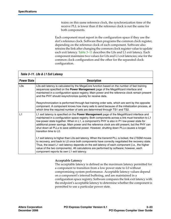
Specifications
trains on this same reference clock, the synchronization time of the receive PLL is lower than if the reference clock is not the same for both components.
Each component must report in the configuration space if they use the slot’s reference clock. Software then programs the common clock register, depending on the reference clock of each component. Software also retrains the link after changing the common clock register value to update each exit latency. Table 3–11 describes the L0s and L1 exit latency. Each component maintains two values for L0s and L1 exit latencies; one for the common clock configuration and the other for the separated clock configuration.
Acceptable LatencyThe acceptable latency is defined as the maximum latency permitted for a component to transition from a low power state to L0 without compromising system performance. Acceptable latency values depend on a component’s internal buffering, and are maintained in a configuration space registry. Software compares the link exit latency with the endpoint’s acceptable latency to determine whether the component is permitted to use a particular power state.
Table 3–11. L0s & L1 Exit Latency
Power State Description
L0s L0s exit latency is calculated by the MegaCore function based on the number of fast training sequences specified on the Power Management page of the MegaWizard interface and maintained in a configuration space registry. Main power and the reference clock remain present and the PHY should resynchronize quickly for receive data.
Resynchronization is performed through fast training order sets, which are sent by the opposite component. A component knows how many sets to send because of the initialization process, at which time the required number of sets are determined through TS1 and TS2.
L1 L1 exit latency is specified on the Power Management page of the MegaWizard interface and maintained in a configuration space registry. Both components across a link must transition to L1 low-power state together. When in L1, a component’s PHY is also in P1 low-power state for additional power savings. Main power and the reference clock are still present, but the PHY can shut down all PLLs to save additional power. However, shutting down PLLs causes a longer transition time to L0.
L1 exit latency is higher than L0s exit latency. When the transmit PLL is locked, the LTSSM moves to recovery, and back to L0 once both components have correctly negotiated the recovery state. Thus, the exact L1 exit latency depends on the exit latency of each component (i.e., the higher value of the two components). All calculations are performed by software; however, each component reports its own L1 exit latency.
Altera Corporation PCI Express Compiler Version 6.1 3–23December 2006 PCI Express Compiler User Guide

Functional Description
■ For L0s, the opposite component and the exit latency of each component between the root port and endpoint is compared with the endpoint’s acceptable latency. For example, for an endpoint connected to a root port, if the root port’s L0s exit latency is 1 µs and the endpoint’s L0s acceptable latency is 512 ns, software will probably not enable the entry to L0s for the endpoint.
■ For L1, software calculates the L1 exit latency of each link between the endpoint and the root port, and compares the maximum value with the endpoint’s acceptable latency. For example, for an endpoint connected to a root port, if the root port’s L1 exit latency is 1.5 µs and the endpoint’s L1 exit latency is 4 µs, and the endpoint acceptable latency is 2 µs, the exact L1 exit latency of the link will be 4 µs and software will probably not enable the entry to L1.
Some time adjustment may be necessary if one or more switches are located between the endpoint and the root port.
1 To maximize performance, Altera recommends that you set L0s and L1 acceptable latency values to their minimum values.
Error Handling
Each PCI Express compliant device must implement a basic level of error management and can optionally implement advanced error management. The MegaCore function does both, as described in this section. Given its position and role within the fabric, error handling for a root port is more complex than that of an endpoint.
The PCI Express specifications defines three types of errors, outlined in Table 3–12.
Table 3–12. Error Classification
Type Responsible Agent Description
Correctable Hardware While correctable errors may affect system performance, data integrity is maintained.
Uncorrectable, Non-Fatal Device Software Uncorrectable nonfatal errors are defined as errors in which data is lost, but system integrity is maintained, i.e., the fabric may lose a particular TLP, but it still works without problems.
Uncorrectable, Fatal System Software Errors generated by a loss of data and system failure are considered uncorrectable and fatal. Software must determine how to handle such errors: whether to reset the link or implement other means to minimize the problem.
3–24 PCI Express Compiler Version 6.1 Altera CorporationPCI Express Compiler User Guide December 2006
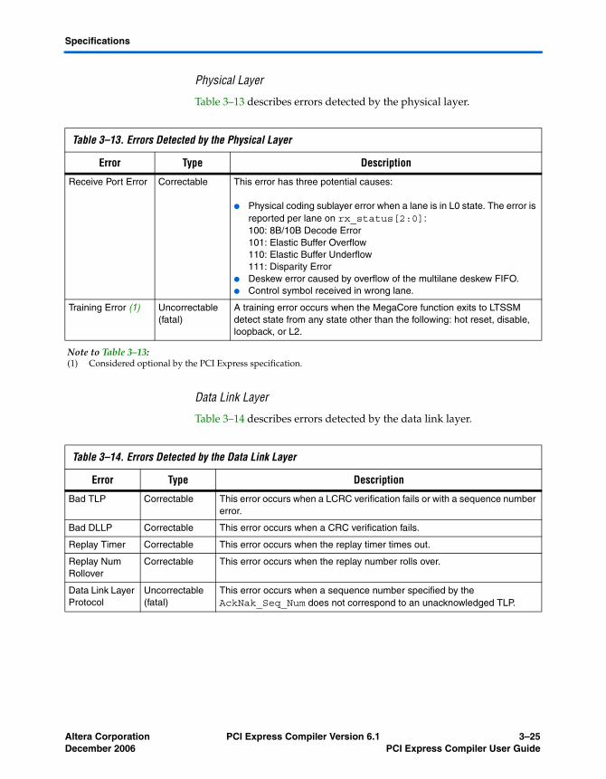
Specifications
Physical Layer
Table 3–13 describes errors detected by the physical layer.
Data Link Layer
Table 3–14 describes errors detected by the data link layer.
Table 3–13. Errors Detected by the Physical Layer
Error Type Description
Receive Port Error Correctable This error has three potential causes:
● Physical coding sublayer error when a lane is in L0 state. The error is reported per lane on rx_status[2:0]:100: 8B/10B Decode Error101: Elastic Buffer Overflow110: Elastic Buffer Underflow111: Disparity Error
● Deskew error caused by overflow of the multilane deskew FIFO.● Control symbol received in wrong lane.
Training Error (1) Uncorrectable(fatal)
A training error occurs when the MegaCore function exits to LTSSM detect state from any state other than the following: hot reset, disable, loopback, or L2.
Note to Table 3–13:(1) Considered optional by the PCI Express specification.
Table 3–14. Errors Detected by the Data Link Layer
Error Type Description
Bad TLP Correctable This error occurs when a LCRC verification fails or with a sequence number error.
Bad DLLP Correctable This error occurs when a CRC verification fails.
Replay Timer Correctable This error occurs when the replay timer times out.
Replay Num Rollover
Correctable This error occurs when the replay number rolls over.
Data Link Layer Protocol
Uncorrectable(fatal)
This error occurs when a sequence number specified by the AckNak_Seq_Num does not correspond to an unacknowledged TLP.
Altera Corporation PCI Express Compiler Version 6.1 3–25December 2006 PCI Express Compiler User Guide

Functional Description
Transaction Layer
Table 3–15 describes errors detected by the transaction layer.
Table 3–15. Errors Detected by the Transaction Layer (Part 1 of 2)
Error Type Description
Poisoned TLP Received
Uncorrectable (Non-Fatal)
This error occurs if a received transaction layer packet has the EP poison bit set.The received TLP is presented on the rx_desc and rx_data busses and the application layer logic must take application appropriate action in response to the poisoned TLP.
ECRC Check Failed (1)
Uncorrectable (Non-Fatal)
This error is caused by an ECRC check failing despite the fact that the transaction layer packet is not malformed and the LCRC check is valid.The MegaCore function handles this transaction layer packet automatically. If the TLP is a non-posted request, the MegaCore function generates a completion with completer abort status. In all cases the TLP is deleted internal to the MegaCore function and not presented to the application layer.
Unsupported Request
Uncorrectable (Non-Fatal)
This error occurs whenever a component receives an unsupported request, including any of the following:
● Completion transaction for which the RID does not match the bus/device.
● Unsupported message.● A type 1 configuration request transaction layer packet.● A locked memory read (MEMRDLK) on native endpoint.● A locked completion transaction.● A 64-bit memory transaction in which the 32 MSBs of an address are
set to 0.● A memory or I/O transaction for which there is no BAR match.
If the TLP is a non-posted request the MegaCore function generates a completion with unsupported request status. In all cases the TLP is deleted internal to the MegaCore function and not presented to the application layer.
Completion Timeout
Uncorrectable (Non-Fatal)
This error occurs when a request originating from the application layer does not generate a corresponding completion transaction layer packet within the established time. It is the responsibility of the application layer logic to provide the completion timeout mechanism. The completion timeout should be reported to the transaction layer via the cpl_err[0] signal.
Completer Abort (1)
Uncorrectable (Non-Fatal)
The application layer reports this error via the cpl_err[1]signal when it aborts reception of a transaction layer packet.
Unexpected Completion
Uncorrectable (Non-Fatal)
This error is caused by an unexpected completion transaction, either input from the application layer via the cpl_err[2] signal or when the requestor ID does not match the endpoint's configured ID.
3–26 PCI Express Compiler Version 6.1 Altera CorporationPCI Express Compiler User Guide December 2006
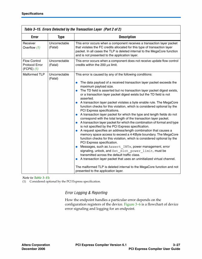
Specifications
Error Logging & Reporting
How the endpoint handles a particular error depends on the configuration registers of the device. Figure 3–6 is a flowchart of device error signaling and logging for an endpoint.
Receiver Overflow (1)
Uncorrectable (Fatal)
This error occurs when a component receives a transaction layer packet that violates the FC credits allocated for this type of transaction layer packet. In all cases the TLP is deleted internal to the MegaCore function and is not presented to the application layer.
Flow Control Protocol Error (FCPE) (1)
Uncorrectable (Fatal)
This error occurs when a component does not receive update flow control credits within the 200 μs limit.
Malformed TLP Uncorrectable (Fatal)
This error is caused by any of the following conditions:
● The data payload of a received transaction layer packet exceeds the maximum payload size.
● The TD field is asserted but no transaction layer packet digest exists, or a transaction layer packet digest exists but the TD field is not asserted.
● A transaction layer packet violates a byte enable rule. The MegaCore function checks for this violation, which is considered optional by the PCI Express specifications.
● A transaction layer packet for which the type and length fields do not correspond with the total length of the transaction layer packet.
● A transaction layer packet for which the combination of format and type is not specified by the PCI Express specification.
● A request specifies an address/length combination that causes a memory space access to exceed a 4-KByte boundary. The MegaCore function checks for this violation, which is considered optional by the PCI Express specification.
● Messages, such as Assert_INTx, power management, error signaling, unlock, and Set_Slot_power_limit, must be transmitted across the default traffic class.
● A transaction layer packet that uses an uninitialized virtual channel.
The malformed TLP is deleted internal to the MegaCore function and not presented to the application layer.
Note to Table 3–15:(1) Considered optional by the PCI Express specification.
Table 3–15. Errors Detected by the Transaction Layer (Part 2 of 2)
Error Type Description
Altera Corporation PCI Express Compiler Version 6.1 3–27December 2006 PCI Express Compiler User Guide

Functional Description
Figure 3–6. Endpoint Device Error Logging & Reporting
Is the detectederror correctable?
Adjust severity accordingto uncorrectable error
severity register.
Set fatal/nonfatal errordetected bit in device
status register.
Set corresponding bitin uncorrectable error
status register.
If first error pointer is notvalid, update first error
pointer and header registers.
Set correctable errordetected bit in device
status register.
Set corresponding bitin correctable error
status register.
Masked inuncorrectable error mask
register?
Masked incorrectable error mask
register?
Uncorrectable errorreporting enabled in device
control register? Correctable errorreporting enabled in device
control register?
Fatal?
YesNo
End
End
End
End
Yes
NoYes
No
Yes
No
Yes
No
YesNo
Send ERR_FATALMessage
End
Send ERR_NONFATALMessage
End
Send ERR_CORRMessage
End
Advanced Error Management Only
Start
3–28 PCI Express Compiler Version 6.1 Altera CorporationPCI Express Compiler User Guide December 2006

Specifications
Data Poisoning
The MegaCore function implements data poisoning, a mechanism for indicating that the data associated with a transaction is corrupted. Poisoned transaction layer packets have the error/poisoned bit of the header set to 1 and observe the following rules:
■ Received poisoned transaction layer packets are sent to the application layer and status bits are automatically updated in the configuration space.
■ Received poisoned configuration write transaction layer packets are not written in the configuration space.
■ The configuration space never generates a poisoned transaction layer packet, i.e., the error/poisoned bit of the header is always set to 0.
Poisoned transaction layer packets can also set the parity error bits in the PCI configuration space status register. Parity errors are caused by the conditions specified in Table 3–16.
Poisoned packets received by the MegaCore function are passed to the application layer. Poisoned transmit transaction layer packets are likewise sent to the link.
Stratix GX PCI Express Compatibility
If during the PCI Express receiver detection sequence, some other PCI Express devices cannot detect the Stratix GX receiver, the other device remains in the LTSSM Detect state, the Stratix GX device remains in the Compliance state, and the link is not initialized. This occurs because Stratix GX devices do not exhibit the correct receiver impedance characteristics when the receiver input is at electrical idle. Stratix GX devices were designed before the PCI Express specification was
Table 3–16. Parity Error Conditions
Status Bit Conditions
Detected Parity Error (status register bit 15)
Set when any received transaction layer packet is poisoned.
Master Data Parity Error (status register bit 8)
This bit is set when the command register parity enable bit is set and one of the following conditions is true:
● Transmission of a write request transaction layer packet with poisoned bit set. ● Reception of a completion transaction layer packet with poison bit set.
Altera Corporation PCI Express Compiler Version 6.1 3–29December 2006 PCI Express Compiler User Guide
Functional Description
developed. Stratix II GX devices were designed to meet the PCI Express protocol and do not have this issue. However, a Stratix II GX is one of the PCI Express devices that is unable to detect Stratix GX.
The resulting design impact is that Stratix GX will not interoperate with some other PCI Express devices. However, you can workaround this issue by doing either of the following:
■ If possible, force the other PCI Express device to ignore the results of the Rx Detect protocol and try to train the link anyway.
■ Migrate Stratix GX PCI Express designs to Stratix II GX.
OpenCore Plus Time-Out Behavior
OpenCore® Plus hardware evaluation can support the following two modes of operation:
■ Untethered—the design runs for a limited time■ Tethered—requires a connection between your board and the host
computer. If tethered mode is supported by all MegaCore functions in a design, the device can operate for a longer time or indefinitely
All MegaCore functions in a device time out simultaneously when the most restrictive evaluation time is reached. If there is more than one MegaCore function in a design, a specific MegaCore function’s time-out behavior may be masked by the time-out behavior of the other MegaCore functions.
1 For MegaCore functions, the untethered time out is 1 hour; the tethered time-out value is indefinite.
When the hardware evaluation time expires, the MegaCore function does the following:
1. The link training and status state machine are forced to the detect quiet state and held there. This disables the PCI Express link preventing additional data transfer.
2. The PCI Express capability registers in the configuration space are held in a reset state.
f For more information on OpenCore Plus hardware evaluation, see “OpenCore Plus Evaluation” on page 1–6 and AN 320: OpenCore Plus Evaluation of Megafunctions.
3–30 PCI Express Compiler Version 6.1 Altera CorporationPCI Express Compiler User Guide December 2006

Specifications
Parameter Settings
This section describes the PCI Express function parameters, which can only be set using the MegaWizard interface Parameter Settings tab.
System Settings Page
The first page of the MegaWizard interface contains the parameters for the overall system settings and the base address registers. See Figure 3–7.
Figure 3–7. System Settings Page
Altera Corporation PCI Express Compiler Version 6.1 3–31December 2006 PCI Express Compiler User Guide

Parameter Settings
Table 3–17 describes the parameters you can set on this page.
Table 3–17. System Settings Page Parameters (Part 1 of 2)
Parameter Value Description
PHY type Custom Allows all PHY interfaces (except serial), allows x1 and x4 lanes
Stratix GX Stratix GX uses the Stratix GX device family's built-in altgxb transceiver. Selecting this PHY allows only a serial PHY interface and restricts the Number of Lanes to be x1 or x4.
Stratix II GX Stratix II GX uses the Stratix II GX device family's built-in alt2gxb transceiver. Selecting this PHY allows only serial PHY interface and the Number of Lanes can be x1, x4, or x8.
TI XIO1100 TI XIO1100 allows an 8 -bit DDR with a transmit clock (txclk) or a 16-bit SDR with a transmit clock PHY interface. Both of these restricts the Number of Lanes to x1.
Philips PX1011A Philips PX1011A uses a PHY interface of 8-bit SDR with a TxClk. This option restricts the number of lanes to x1.
PHY interface Serial, 16-bit SDR,16-bit SDR w/TxClk, 8-bit DDR, 8-bit DDR w/TxClk, 8-bit SDR,8-bit SDR w/TxClk
This selects the specific type of external PHY interface based on datapath width and clocking mode. See Chapter 4, External PHYs for additional detail on specific PHY modes. Stratix II GX and Stratix GX are serial only PHY interfaces, and they are the only available serial interfaces.
Lanes x1, x4, x8 Specifies the maximum number of lanes supported.The x8 value is supported only for a Stratix II GX PHY.
Port type Native Endpoint, Legacy Endpoint
Specifies the port type. Altera recommends Native endpoint for all new designs. Select Legacy Endpoint only when you require I/O transaction support for compatibility. See “Endpoint Types” on page 3–2 for more information.
Xcvr ref_clk 100 MHz, 125 MHz, 156.25 MHz
Specifies the frequency of the refclk input clock signal when using the Stratix GX PHY. The Stratix GX PHY can use either a 125- or 156.25-MHz clock directly. If you select 100 MHz, the MegaCore function uses a Stratix GX PLL to create a 125-MHz clock from the 100-MHz input.
If you use a generic PIPE, the refclk is not required.A Stratix II GX PHY requires a 100 MHz clock.
PCI Express version 1.0A or 1.1 Selects the PCI Express specification that the variation will be compatible with
3–32 PCI Express Compiler Version 6.1 Altera CorporationPCI Express Compiler User Guide December 2006

Specifications
MegaCore Function BAR Support
The x1 and x4 MegaCore functions support Memory Space BARs ranging in size from 128 bytes to the maximum allowed by a 32-bit or 64-bit BAR. The x8 MegaCore functions support Memory Space BARs from 4 KBytes to the maximum allowed by a 32-bit or 64-bit BAR.
The x1 and x4 MegaCore functions in Legacy Endpoint mode support I/O Space BARs sized from 16 Bytes to 4 KBytes. The x8 MegaCore function only supports I/O Space BARs of 4 KBytes.
Configure transceiver block
Enable fast recovery mode or Enable rate match fifo
Displays a dialog box that allows you to configure the transceiver block. This option is valid only when you select a Stratix II GX PHY. See Table 3–18 and Figure 3–8 for details on these available options.
Internal clock 62.5, 125, 250 MHz Specifies the frequency of the internal clock which is based on the number of lanes and the selected PHY type. This is also the frequency at which the application layer interface of the core operates.
For x8 configurations, the internal clock is fixed at 250 MHz. For x4 configurations, the internal clock is fixed at 125 MHz. For x1 configurations in Stratix II GX, the internal clock is fixed at 125 MHz. For other x1 configurations, the Internal Clock can be selected to be either 62.5 MHz or 125 MHz.
BAR Table (BAR0) BAR type and size BAR0 size and type mapping (I/O space, memory space, prefetchable). BAR0 and BAR1 can be combined to form a 64-bit BAR.
BAR Table (BAR1) BAR type and size BAR1 size and type mapping (I/O space, memory space, prefetchable).
BAR Table (BAR2) BAR type and size BAR2 size and type mapping (I/O space, memory space, prefetchable). BAR2 and BAR3 can be combined to form a 64-bit BAR.
BAR Table (BAR3) BAR type and size BAR3 size and type mapping (I/O space, memory space, prefetchable).
BAR Table (BAR4) BAR type and size BAR4 size and type mapping (I/O space, memory space, prefetchable).
BAR Table (BAR5) BAR type and size BAR5 size and type mapping (I/O space, memory space, prefetchable). BAR4 and BAR5 can be combined to form a 64-bit BAR.
BAR Table (EXP-ROM) BAR type and size Expansion ROM BAR size and type mapping (I/O space, memory space, prefetchable).
Table 3–17. System Settings Page Parameters (Part 2 of 2)
Parameter Value Description
Altera Corporation PCI Express Compiler Version 6.1 3–33December 2006 PCI Express Compiler User Guide

Parameter Settings
Configure Transceiver Block for Stratix II GX PHY
When you use the Stratix II GX PHY, you can configure the transceiver block by modifying the settings in the dialog box available from Configure transceiver block on the System Settings page.
Figure 3–8. Configure Transceiver Dialog
Table 3–18. Configure Transceiver Block Parameters
Parameter Description
Enable fast recovery mode When enabled this option adds additional logic to allow a faster exit from the Rx ASPM L0s state. When disabled exit from Rx ASPM L0s will typically require link recovery to be invoked.
Enable rate match fifo When enabled this option enables the Rate Matching FIFO to allow different clocks with PPM differences at each end of the PCI Express link.
When disabled the rate match FIFO is bypassed, allowing for lower latency, but it is required that the ports at both ends of the PCI Express link use the same clock source. There can be no PPM difference between the clocks at each end.
3–34 PCI Express Compiler Version 6.1 Altera CorporationPCI Express Compiler User Guide December 2006

Specifications
Capabilities Page Parameters
The Capabilities page contains the parameters for the PCI read-only registers and main capability settings. See Figure 3–9.
Figure 3–9. Capabilities Page
Table 3–19 describes the parameters that you can set on this page.
Table 3–19. Capabilities Page Parameters (Part 1 of 2)
Parameter Value Description
Device ID 16-bit Hex Sets the read-only value of the device ID register.
Vendor ID 16-bit Hex Sets the read-only value of the vendor ID register. This parameter can not be set to 0xFFFF per the PCI Express Specification.
Class code 24-bit Hex Sets the read-only value of the class code register.
Revision ID 8-bit Hex Sets the read-only value of the revision ID register.
Altera Corporation PCI Express Compiler Version 6.1 3–35December 2006 PCI Express Compiler User Guide

Parameter Settings
Subsystem ID 16-bit Hex Sets the read-only value of the subsystem device ID register.
Subsystem vendor ID 16-bit Hex Sets the read-only value of the subsystem vendor ID register. This parameter can not be set to 0xFFFF per the PCI Express Specification.
Link common clock On/Off Indicates if the common reference clock supplied by the system is used as the reference clock for the PHY. This parameter sets the read-only value of the slot clock configuration bit in the link status register.
Implement advanced error reporting
On/Off Implement the advanced error reporting capability.
Implement ECRC check On/Off Enable ECRC checking capability. Sets the read-only value of the ECRC check capable bit in the advanced error capabilities and control register. This parameter requires you to implement the advanced error reporting capability.
Implement ECRC generation
On/Off Enable ECRC generation capability. Sets the read-only value of the ECRC generation capable bit in the advanced error capabilities and control register. This parameter requires you to implement the advanced error reporting capability.
Link port number 8-bit Hex Sets the read-only values of the port number field in the link capabilities register.
Tags supported 4, 8, 16, 32, 64, 128, 256
Indicates the number of tags supported for non-posted requests transmitted by the application layer. The transaction layer tracks all outstanding completions for non-posted requests made by the application. This parameter configures the transaction layer for the maximum number to track. The Application Layer must set the Tag values in all Non-Posted PCI Express headers to be less than this value. Values greater than 32 also set the Extended Tag Field Supported bit in the configuration space device capabilities register. The application can only use tag numbers greater than 31 if configuration software sets the Extended Tag Field Enable bit of the device control register. This bit is available to the application as cfg_devcsr[8]. This value is limited to a maximum of 8 for the x8 MegaCore function.
MSI messages requested 1, 2, 4, 8, 16, 32
Indicates how many messages the application requests. Sets the value of the multiple message capable field of the message control register. See “MSI & INTx Interrupt signals” on page 3–82 for more information.
MSI message 64-bit capable
On/Off Indicates whether the MSI capability message control register is 64-bit addressing capable. PCI Express native endpoints always support MSI 64-bit addressing.
Table 3–19. Capabilities Page Parameters (Part 2 of 2)
Parameter Value Description
3–36 PCI Express Compiler Version 6.1 Altera CorporationPCI Express Compiler User Guide December 2006

Specifications
Buffer Setup Page
The Buffer Setup page contains the parameters for the receive and retry buffers. See Figure 3–10.
Figure 3–10. Buffer Setup Page
Altera Corporation PCI Express Compiler Version 6.1 3–37December 2006 PCI Express Compiler User Guide

Parameter Settings
Table 3–20 describes the parameters you can set on this page.
Table 3–20. Buffer Setup Page Parameters (Part 1 of 3)
Parameter Value Description
Maximum payload size
128 Bytes, 256 Bytes, 512 Bytes, 1 KByte, 2 KBytes
Specify the maximum payload size supported. This parameter sets the Read Only value of the max payload size supported field of the device capabilities register and optimizes the MegaCore function for this size payload.
Number of virtual channels
1 - 4 Specify the number of virtual channels supported. This parameter sets the read-only extended virtual channel count field of the port virtual channel capability register 1 and controls how many virtual channel transaction layer interfaces are implemented.
Number of low priority VCs
None, 2, 3, 4 Specify the number of virtual channels in the low-priority arbitration group. The virtual channels numbered less than this value are low priority. Virtual channels numbered greater than or equal to this value are high priority. See “Transmit Virtual Channel Arbitration” on page 3–5 for more information. This parameter sets the read-only low-priority extended virtual channel count field of the port virtual channel capability register 1.
Auto configure retry buffer size
On/Off Controls automatic configuration of the retry buffer based on the maximum payload size.
Retry buffer size 512 Bytes to 16 KBytes (powers of 2)
Set the size of the retry buffer for storing transmitted PCI Express packets until acknowledged.
Maximum retry packets
4 to 256 (powers of 2)
Set the maximum number of packets that can be stored in the retry buffer.
3–38 PCI Express Compiler Version 6.1 Altera CorporationPCI Express Compiler User Guide December 2006

Specifications
Desired performance for received requests
Low, Medium, High, Maximum
Specify how to configure the Rx Buffer size and the flow control credits.
● Low—Provides the minimal amount of space for desired traffic. Select this option when the throughput of the received requests is not critical to the system design. Doing this will minimize the device resource utilization.
● Medium—Provides a moderate amount of space for received requests. Select this option when the received request traffic does not need to use the full link bandwidth, but is expected to occasionally use bursts of a couple maximum sized payload packets.
● High—Provides enough buffer space to maintain full link bandwidth of received requests with typical external link delays and FC Update processing delays by the attached PCI Express port. Use this setting in most circumstances where full link bandwidth is needed. This is the default.
● Maximum—Provides additional space to allow for additional external delays (link side and application side) and still allows full throughput.
If you need more buffer space than this parameter supplies, select a larger payload size and this setting. Doing this increases the buffer size and slightly increase the number of logic elements (LEs) to support a larger Payload size than will be used.
For more information, see data credits in the section, “Analyzing Throughput” on page 3–11.
Table 3–20. Buffer Setup Page Parameters (Part 2 of 3)
Parameter Value Description
Altera Corporation PCI Express Compiler Version 6.1 3–39December 2006 PCI Express Compiler User Guide

Parameter Settings
Desired performance for received completions
Low, Medium, High, Maximum
Specify how to configure the Rx Buffer size and the flow control credits.
● Low—Provides the minimal amount of space for received completions. Select this option when the throughput of the received completions is not critical to the system design. This would also be used when you application is expected to never initiate read requests on the PCI Express links. Selecting this option will minimize the device resource utilization.
● Medium—Provides a moderate amount of space for received completions. Select this option when the received completion traffic does not need to use the full link bandwidth, but is expected to occasionally use bursts of a couple maximum sized payload packets.
● High—Provides enough buffer space to main full link bandwidth of received requests with typical external link delays and FC Update processing delays by the attached PCI Express port. Use this setting in most circumstances where full link bandwidth is needed. This is the default.
● Maximum—Provides additional space to allow for additional external delays (link side and application side) and still allows full throughput.
If you need more buffer space than this parameter supplies, select a larger payload size and this setting. Doing this increases the buffer size and slightly increase the number of logic elements (LEs) to support a larger Payload size than will be used.
For more information, see data credits in the section, “Analyzing Throughput” on page 3–11.
RX Buffer Space Allocation
Read-Only Table The Rx Buffer Space Allocation table shows the credits and space allocated for each flow-controllable type, based on the Rx Buffer Size setting. All virtual channels use the same Rx Buffer space allocation.
The table does not show non-posted data credits because the MegaCore function always advertises infinite non-posted data credits and automatically has room for the maximum 1 DWORD of data that can be associated with each non-posted header.
The numbers shown for completion headers and completion data indicate how much space is reserved in the Rx Buffer for completions. However, infinite completion credits are advertised on the PCI Express link as is required for endpoints. It is up to the application layer to manage the rate of non-posted requests made to ensure that the Rx Buffer completion space does not overflow.
Table 3–20. Buffer Setup Page Parameters (Part 3 of 3)
Parameter Value Description
3–40 PCI Express Compiler Version 6.1 Altera CorporationPCI Express Compiler User Guide December 2006

Specifications
Power Management Page
The Power Management page contains the parameters for setting various power management properties of the MegaCore function. See Figure 3–11.
Figure 3–11. Power Management Page
Altera Corporation PCI Express Compiler Version 6.1 3–41December 2006 PCI Express Compiler User Guide

Parameter Settings
Table 3–21 describes the parameters you can set on this page.
Table 3–21. Power Management Page Parameters (Part 1 of 2)
Parameter Value Description
Idle threshold for L0s entry
256 ns to 8,192 ns (in 256-ns increments)
Indicate the idle threshold for L0s entry. This parameter specifies the amount of time the link must be idle before the transmitter transitions to L0s state. The PCI Express specification states that this time should be no more than 7 μs, but the exact value is implementation-specific. If you select the Stratix GX PHY or Stratix II GX PHY, this parameter is disabled and set to its maximum value If you are using an external PHY; consult the PHY vendor's documentation to determine the correct value for this parameter.
Endpoint L0s acceptable latency
< 64 ns to > 4 μs Indicate the acceptable endpoint L0s latency for the device capabilities register. Sets the read-only value of the endpoint L0s acceptable latency field of the device capabilities register. This value should be based on how much latency the application layer can tolerate.
Number of Fast TrainingSequencesCommon clock
0 - 255 Indicate the number of fast training sequences needed in common clock mode. The number of fast training sequences required is transmitted to the other end of the link during link initialization and is also used to calculate the L0s exit latency field of the device capabilities register. If you select the Stratix GX PHY or Stratix II GX PHY, this parameter is disabled and set to its maximum value. If you are using an external PHY, consult the PHY vendor's documentation to determine the correct value for this parameter.
Number of Fast TrainingSequences Separate clock
0 - 255 Indicate the number of fast training sequences needed in separate clock mode. The number of fast training sequences required is transmitted to the other end of the link during link initialization and is also used to calculate the L0s exit latency field of the device capabilities register. If you select the Stratix GX PHY or Stratix II GX PHY, this parameter is disabled and set to its maximum value. If you are using an external PHY, consult the PHY vendor's documentation to determine the correct value for this parameter.
Enable L1 ASPM On/Off Set the L1 active state power management support bit in the link capabilities register. If you select the Stratix GX PHY or Stratix II GX PHY, this option is turned off and disabled.
Endpoint L1 acceptable latency
< 1μs to > 64 μs Indicate the endpoint L1 acceptable latency. Sets the read-only value of the endpoint L1 acceptable latency field of the device capabilities register. This value should be based on how much latency the application layer can tolerate.
3–42 PCI Express Compiler Version 6.1 Altera CorporationPCI Express Compiler User Guide December 2006

Specifications
Signals The application interface has four categories of signals:
■ Transmit data path interface signals■ Receive data path interface signals■ Configuration interface signals■ Global signals
Figure 3–12 shows all PCI Express MegaCore function signals.
Transmit and receive signals apply to each implemented virtual channel, while configuration and global signals are common to all virtual channels on a link.
L1 Exit Latency Common clock
< 1μs to > 64 μs Indicate the L1 exit latency for the separate clock. Used to calculate the value of the L1 exit latency field of the device capabilities register. If you select the Stratix GX PHY or Stratix II GX PHY, this parameter is disabled and set to its maximum value. If you are using an external PHY, consult the PHY vendor's documentation to determine the correct value for this parameter.
L1 Exit Latency Separate clock
< 1μs to > 64 μs Indicate the L1 exit latency for the common clock. Used to calculate the value of the L1 exit latency field of the device capabilities register. If you select the Stratix GX PHY or Stratix II GX PHY, this parameter is disabled and set to its maximum value. If you are using an external PHY, consult the PHY vendor's documentation to determine the correct value for this parameter.
Table 3–21. Power Management Page Parameters (Part 2 of 2)
Parameter Value Description
Altera Corporation PCI Express Compiler Version 6.1 3–43December 2006 PCI Express Compiler User Guide

Signals
Figure 3–12. MegaCore Function I/O Signals
tx_req0
tx_desc0
tx_ack0
tx_dfr0
tx_dv0
tx_data0[63:0]
tx_ws0
tx_cred0[21:0]
rx_req0
rx_desc0[135:0]
rx_ack0
rx_abort0
rx_retry0
rx_mask0
rx_dfr0
rx_dv0
rx_data0[63:0]
rx_be0[7:0]
rx_ws0
pme_to_cr
pme_to_sr
cfg_pmcsr[31:0]
app_msi_req
app_msi_ack
ack_msi_tc[2:0]
msi_num[4:0]
cfg_msicsr[15:0]
pex_msi_num[4:0]
app_int_sts
refclk
clk125_in
clk125_out
npor
srst
crst
12_exit
hotrst_exit
dlup_exit
cfg_tcvcmap[23:0]
cfg_busdev[12:0]
cfg_prmcfr[31:0]
cfg_devcsr[31:0]
cfg_linkcsr[31:0]
cpl_err[2:0]
cpl_pending
test_in[31:0]
test_out[511:0]
PCI Express MegaCore Function
1-Bit Serial
tx[7:0]
rx[7:0]
pipe_mode
txdata0_ext[15:0]
txdatak0_ext[1:0]
txdetectrx0_ext
txelecidle0_ext
txcompliance0_ext
rxpolarity0_ext
powerdown0_ext[1:0]
rxdata0_ext[15:0]
rxdatak0_ext[1:0]
rxvalid0_ext
phystatus0_ext
rxelecidle0_ext
rxstatus0_ext[2:0]
16-Bit PIPE for x1 and x4 (Repeated for Lanes 1 - 3 in the x4 MegaCore Function)
Transmit Data Path (for VC0)
Receive Data Path (for VC0)
Power Management
Interrupt
Global
Configuration
Completion Interface
Test Interface
txdata0_ext[7:0]
txdatak0_ext
txdetectrx0_ext
txelecidle0_ext
txcompliance0_ext
rxpolarity0_ext
powerdown0_ext[1:0]
rxdata0_ext[7:0]
rxdatak0_ext
rxvalid0_ext
phystatus0_ext
rxelecidle0_ext
rxstatus0_ext[2:0]
8-Bit PIPE for x8(Repeated for Lanes 1 - 7in the x8 MegaCore Function)
(1)
(2)
(3)
(3)
(4)
Notes SignalChanges for x 8 MegaCore Functions: (1) clk125_in for the x1, x4 MegaCore function is changed to clk250_in for a x8 MegaCore function(2) clk125_out for the x1 or x4 MegaCore function is changed to clk250_out for the x8 MegaCore function (3) srst & crst are removed for the x8 MegaCore function(4) test_out[511:0] for the x1 or x4 MegaCore function is changed to test_out[127:0] for the x8 MegaCore function.
3–44 PCI Express Compiler Version 6.1 Altera CorporationPCI Express Compiler User Guide December 2006

Specifications
Transmit Interface Operation Signals
The transmit interface is established per initialized virtual channel and is based on two independent busses, one for the descriptor phase (tx_desc[127:0]) and one for the data phase (tx_data[63:0]). Every transaction includes a descriptor. A descriptor is a standard transaction layer packet header as defined by the PCI Express Base Specification Revision 1.0a with the exception of bits 126 and 127, which indicate the transaction layer packet group as described in the following section. Only transaction layer packets with a normal data payload include one or more data phases.
Transmit Data Path Signals
The MegaCore function assumes that transaction layer packets sent by the application layer are well-formed, i.e., the MegaCore function will not detect if the application layer sends it a malformed transaction layer packet.
Transmit data path signals can be divided into two groups:
■ Descriptor Phase signals■ Data Phase signals
1 In the following tables, transmit interface signal names suffixed with 0 are for virtual channel 0. If the MegaCore function implements additional virtual channels, there are an additional set of signals suffixed with the virtual channel number.
Altera Corporation PCI Express Compiler Version 6.1 3–45December 2006 PCI Express Compiler User Guide

Signals
Table 3–22 describes the standard descriptor phase signals.
Table 3–22. Standard Descriptor Phase Signals
Signal I/O Description
tx_reqn (1), (2) I Transmit request. This signal must be asserted for each request. It is always asserted with the tx_desc[127:0] and must remain asserted until tx_ack is asserted. This signal does not need to be deasserted between back-to-back descriptor packets.
tx_descn[127:0](1), (2)
I Transmit descriptor bus. The transmit descriptor bus, bits 127:0 of a transaction, can include a 3 or 4 DWORDS PCI Express transaction header. Bits have the same meaning as a standard transaction layer packet header as defined by the PCI Express Base Specification Revision 1.0a. Byte 0 of the header occupies bits 127:120 of the tx_desc bus, byte 1 of the header occupies bits 119:112, and so on, with byte 15 in bits 7:0. See Appendix B, Transaction Layer Packet Header Formats for the header formats.
The following bits have special significance:
● tx_desc[2] or tx_desc[34] indicate the alignment of data on tx_data.● tx_desc[2] (64-bit address) set to 0: The first DWORD is located on
tx_data[31:0].● tx_desc[34] (32-bit address) set to 0: The first DWORD is located on bits
tx_data[31:0].● tx_desc[2] (64-bit address) set to 1: The first DWORD is located on bits
tx_data[63:32].● tx_desc[34] (32-bit address) set to 1: The first DWORD is located on bits
tx_data[63:32].
Bit 126 of the descriptor indicates the type of transaction layer packet in transit:
● tx_desc[126] set to 0: transaction layer packet without data● tx_desc[126] set to 1: transaction layer packet with data
The following list provides a few examples of bit placement on this bus:
● tx_desc[105:96]: length[9:0]● tx_desc[126:125]: fmt[1:0]● tx_desc[126:120]: type[4:0]
tx_ackn(1), (2)
O Transmit acknowledge. This signal is asserted for one clock cycle when the MegaCore function acknowledges the descriptor phase requested by the application through the tx_req signal. On the following clock cycle, a new descriptor can be requested for transmission through the tx_req signal (kept asserted) and the tx_desc.
Notes for Table 3–22(1) where n is the virtual channel number; For x1 and x4, n can be 0 - 3(2) For x8, n can be 0 or 1
3–46 PCI Express Compiler Version 6.1 Altera CorporationPCI Express Compiler User Guide December 2006

Specifications
Table 3–23 describes the standard data phase signals.
Table 3–23. Standard Data Phase Signals (Part 1 of 2)
Signal I/O Description
tx_dfrn(1), (2)
I Transmit data phase framing. This signal is asserted on the same clock cycle as tx_req to request a data phase (assuming a data phase is needed). This signal must be kept asserted until the clock cycle preceding the last data phase.
tx_dvn(1), (2)
I Transmit data valid. This signal is asserted by the user application interface to signify that the tx_data[63:0] signal is valid. This signal must be asserted on the clock cycle following assertion of tx_dfr until the last data phase of transmission. The MegaCore function will accept data only when this signal is asserted and as long as tx_ws is not asserted.
The application interface can rely on the fact that the first data phase will never occur before a descriptor phase is acknowledged (through assertion of tx_ack). However, the first data phase can coincide with assertion of tx_ack if the transaction layer packet header is only 3 DWORDS.
tx_wsn(1), (2)
O Transmit wait states. This signal is used by the MegaCore function to insert wait states to prevent data loss. This signal might be used in the following circumstances:
● To give a DLLP transmission priority.● To give a high-priority virtual channel or the retry buffer transmission priority
when the link is initialized with fewer lanes than are permitted by the link.
If the MegaCore function is not ready to acknowledge a descriptor phase (through assertion of tx_ack), it will automatically assert tx_ws to throttle transmission.When tx_dv is not asserted, tx_ws should be ignored.
Altera Corporation PCI Express Compiler Version 6.1 3–47December 2006 PCI Express Compiler User Guide

Signals
Table 3–24 describes the advanced data phase signals.
tx_datan[63:0](1), (2)
I Transmit data bus. This signal transfers data from the application interface to the link. It is 2 DWORDS wide and is naturally aligned with the address in one of two ways, depending on bit 2 of the transaction layer packet address, which is located on bit 2 or 34 of the tx_desc (depending on the 3 or 4 DWORDS transaction layer packet header bit 125 of the tx_desc signal).
● tx_desc[2] (64-bit address) set to 0: The first DWORD is located on tx_data[31:0].
● tx_desc[34] (32-bit address) set to 0: The first DWORD is located on bits tx_data[31:0].
● tx_desc[2](64-bit address) set to 1: The first DWORD is located on bits tx_data[63:32].
● tx_desc[34] (32-bit address) set to 1: The first DWORD is located on bits tx_data[63:32].
This natural alignment allows you to connect the tx_data[63:0] directly to a 64-bit data path aligned on a QWORD address (in the little endian convention).
Bit 2 is set to 1 (5 DWORDS transaction).
Bit 2 is set to 0 (5 DWORDS transaction).
Notes for Table 3–23(1) where n is the virtual channel number; For x1 and x4, n can be 0 - 3(2) For x8, n can be 0 or 1
Table 3–23. Standard Data Phase Signals (Part 2 of 2)
Signal I/O Description
tx_data[63:32]
tx_data[31:0]
1 2 3 4 5 6
Clock Cycles
X DW 2DW 0 XDW 4
X DW 3DW 1 X
tx_data[63:32]
tx_data[31:0]
1 2 3 4 5 6
Clock Cycles
X DW 2DW 0 XDW 4
X DW 3DW 1 X
3–48 PCI Express Compiler Version 6.1 Altera CorporationPCI Express Compiler User Guide December 2006

Specifications
Table 3–24. Advanced Data Phase Signals
Signal I/O Description
tx_credn[65:0](1),(2)
O Transmit credit. This signal is used to inform the application layer whether it can transmit a transaction layer packet of a particular type based on available flow control credits. This signal is optional because the MegaCore function always checks for sufficient credits before acknowledging a request. However, by checking available credits with this signal, the application can improve system performance by dividing a large transaction layer packet into smaller transaction layer packets based on available credits or arbitrating among different types of transaction layer packets by sending a particular transaction layer packet across a virtual channel that advertises available credits. See Table 3–25 for the bit detail.
Once a transaction layer packet is acknowledged by the MegaCore function, the corresponding flow control credits are consumed and this signal is updated 1 clock cycle after assertion of tx_ack.
For a component that has received infinite credits at initialization, each field of this signal is set to its highest potential value.
For the x1 and x4 MegaCore functions this signal is 22 bits wide with some encoding of the available credits to make it easier for the application layer to check the available credits. Table 3–22 for details.
In the x8 MegaCore function this signal is 66 bits wide and provides the exact number of available credits for each flow control type. See Table 3–26 for details.
tx_errn(1)
I Transmit error. This signal is used to discard or nullify a transaction layer packet, and is asserted for one clock cycle during a data phase. The MegaCore function will automatically commit the event to memory and wait for the end of the data phase.
Upon assertion of tx_err, the application interface should stop transaction layer packet transmission by deasserting tx_dfr and tx_dv.
This signal only applies to transaction layer packets sent to the link (as opposed to transaction layer packets sent to the configuration space). If unused, this signal can be tied to zero. This signal is not available in the x8 MegaCore function.
Notes for Table 3–24(1) where n is the virtual channel number; For x1 and x4, n can be 0 - 3(2) For x8, n can be 0 or 1
Altera Corporation PCI Express Compiler Version 6.1 3–49December 2006 PCI Express Compiler User Guide

Signals
Table 3–25 shows the bit information for tx_cred0[21:0] for the x1 and x4 MegaCore functions.
Table 3–26 shows the bit information for tx_credn[65:0] for the x8 MegaCore functions.
Table 3–25. tx_cred0[21:0] Bits for the x1 and x4 MegaCore Functions
Bit Value Description
0 ● 0: No credits available● 1: Sufficient credit available for at least 1
transaction layer packet
Posted header.
9:1 ● 0: No credits available● 1-256: number of credits available● 257-511: reserved
Posted data: 9 bits permit advertisement of 256 credits, which corresponds to 4KBytes, the maximum payload size.
10 ● 0: No credits available● 1: Sufficient credit available for at least 1
transaction layer packet
Non-Posted header.
11 ● 0: No credits available● 1: Sufficient credit available for at least 1
transaction layer packet
Non-Posted data.
12 ● 0: No credits available● 1: Sufficient credit available for at least 1
transaction layer packet
Completion header.
21:13 9 bits permit advertisement of 256 credits, which corresponds to 4 KBytes, the maximum payload size.
Completion data, posted data.
Table 3–26. tx_cred[65:0] bits for x8 MegaCore Function (Part 1 of 2)
Bit Value Description
tx_cred[7:0] ● 0 No credits available● 1 Sufficient credit available for at least 1
TLP
Posted header Ignore this field if the value of Posted Header credits, tx_cred[60], are set to 1.
tx_cred[19:8] ● 0: No credits available● 1-256: number of credits available● 257-511: reserved
Posted Data: 9 bits permit advertisement of 256 credits, which corresponds to 4KB, the Maximum Payload Size. Ignore this field if value of the Posted Data credits, tx_cred[61], set to 1.
tx_cred[27:20]
● 0: No credits available● 1: Sufficient credit available for at least 1
TLP
Non-Posted HeaderIgnore this field if value of the Non-Posted Header credits, tx_cred[62], set to 1.
3–50 PCI Express Compiler Version 6.1 Altera CorporationPCI Express Compiler User Guide December 2006
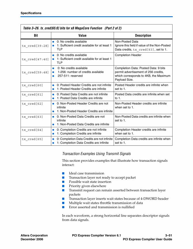
Specifications
Transaction Examples Using Transmit Signals
This section provides examples that illustrate how transaction signals interact:
■ Ideal case transmission■ Transaction layer not ready to accept packet■ Possible wait state insertion■ Priority given elsewhere■ Transmit request can remain asserted between transaction layer
packets■ Transaction layer inserts wait states because of 4-DWORD header■ Multiple wait states throttle transmission of data■ Error asserted and transmission is nullified
In each waveform, a strong horizontal line separates descriptor signals from data signals.
tx_cred[39:28]
● 0: No credits available● 1: Sufficient credit available for at least 1
TLP
Non-Posted DataIgnore this field if value of the Non-Posted Data credits, tx_cred[63], set to 1.
tx_cred[47:40]
● 0: No credits available● 1: Sufficient credit available for at least 1
TLP
Completion Header
tx_cred[59:48]
● 0: No credits available● 1-256: number of credits available● 257-511: reserved
Completion Data: Posted Data: 9 bits permit advertisement of 256 credits, which corresponds to 4KB, the Maximum Payload Size.
tx_cred[60] ● 0: Posted Header Credits are not infinite● 1: Posted Header Credits are infinite
Posted Header credits are infinite when set to 1.
tx_cred[61] ● 0: Posted Data Credits are not infinite● 1: Posted Data Credits are infinite
Posted Data credits are infinite.when set to 1.
tx_cred[62] ● 0: Non-Posted Header Credits are not infinite
● 1: Non-Posted Header Credits are infinite
Non-Posted Header credits are infinite when set to 1.
tx_cred[63] ● 0: Non-Posted Data Credits are not infinite
● 1: Non-Posted Data Credits are infinite
Non-Posted Data credits are infinite when set to 1.
tx_cred[64] ● 0: Completion Credits are not infinite● 1: Completion Credits are infinite
Completion Header credits are infinite when set to 1.
tx_cred[65] ● 0: Completion Data Credits are not infinite● 1: Completion Data Credits are infinite
Completion Data credits are infinite when set to 1.
Table 3–26. tx_cred[65:0] bits for x8 MegaCore Function (Part 2 of 2)
Bit Value Description
Altera Corporation PCI Express Compiler Version 6.1 3–51December 2006 PCI Express Compiler User Guide

Signals
Ideal Case TransmissionIn the ideal case, the descriptor and data transfer are independent of each other, and can even happen simultaneously. See Figure 3–13. The MegaCore function transmits a completion transaction of 8 DWORDS. Address bit 2 is set to 0.
In clock cycle 4, the first data phase is acknowledged at the same time as transfer of the descriptor.
Figure 3–13. 64-Bit Completion with Data Transaction of 8 DWORD Waveform
tx_req
tx_ack
tx_desc[127:0]
tx_dfr
tx_dv
tx_data[63:32]
tx_data[31:0]
tx_ws
tx_err
DescriptorSignals
DataSignals
1 2 3 4 5 6 7 8 9 10 11 12 13 14 15
CPLD
DW1 DW3 DW5 DW7X X
DW0 DW2 DW4 DW6X X
Clock Cycles
3–52 PCI Express Compiler Version 6.1 Altera CorporationPCI Express Compiler User Guide December 2006

Specifications
Figure 3–14 shows the MegaCore function transmitting a memory write of 1 DWORD.
Figure 3–14. Transfer for A Single DWORD Write
tx_desc[127:0]
tx_ack
_data[63:32]
tx_ws
1 2 3 4 5 6 7 10 11 12 13 14 15Clock Cycles
tx_err
tx_dfr
tx_req
8 9
tx_dv
tx_data[31:0]
MEMWR32
DW0
X
X
X
X
DescriptorSignals
txData
Signals
Altera Corporation PCI Express Compiler Version 6.1 3–53December 2006 PCI Express Compiler User Guide

Signals
Transaction Layer Not Ready to Accept PacketIn this example, the application transmits a 64-bit memory read transaction of 6 DWORDs. Address bit 2 is set to 0. See Figure 3–15.
Data transmission cannot begin if the MegaCore function’s transaction layer state machine is still busy transmitting the previous packet, as is the case in this example.
Figure 3–15. State Machine Is Busy with the Preceding Transaction Layer Packet Waveform
tx_req
tx_ack
tx_desc[127:0]
tx_dfr
tx_dv
tx_data[63:32]
tx_data[31:0]
tx_ws
tx_err
DescriptorSignals
DataSignals
1 2 3 4 5 6 7 8 9 10 11 12 13 14 15
MEMRD64
Clock Cycles
3–54 PCI Express Compiler Version 6.1 Altera CorporationPCI Express Compiler User Guide December 2006

Specifications
Figure 3–16 shows that the application layer must wait to receive an acknowledge before write data can be transferred.
Figure 3–16. Transaction Layer Not Ready to Accept Packet
Possible Wait State InsertionIf the MegaCore function is not initialized with its maximum potential lanes, data transfer is necessarily hindered. See Figure 3–18. The application transmits a 32-bit memory write transaction of 8 DWORDS. Address bit 2 is set to 0.
In clock cycle 3, data transfer can begin immediately as long as the transfer buffer is not full.
In clock cycle 5, once the buffer is full and the MegaCore function implements wait states to throttle transmission; 4 clock cycles are required per transfer instead of 1 because the MegaCore function is not configured with the maximum possible number of lanes implemented.
Figure 3–17 shows how the transaction layer extends the a data phase by asserting the wait state signal.
tx_desc[127:0]
tx_ack
tx_data[63:32]
tx_ws
1 2 3 4 5 6 7 10 11 12 13 14 15Clock Cycles
tx_err
tx_dfr
tx_req
8 9
tx_dv
tx_data[31:0]
MEMWR32
DW0
X
X
X
X
DescriptorSignals
DataSignals
Altera Corporation PCI Express Compiler Version 6.1 3–55December 2006 PCI Express Compiler User Guide

Signals
Figure 3–17. Transfer with Wait State Inserted for a Single DWORD Write
Figure 3–18. Signal Activity When MegaCore Function Has Fewer than Maximum Potential Lanes Waveform
tx_desc[127:0]
tx_ack
tx_data[63:32]
tx_ws
1 2 3 4 5 6 7 10 11 12 13 14 15Clock Cycles
tx_err
tx_dfr
tx_req
8 9
tx_dv
tx_data[31:0]
MEMWR32
DW0
X
X
X
X
DescriptorSignals
DataSignals
tx_req
tx_ack
tx_desc[127:0]
tx_dfr
tx_dv
tx_data[63:32]
tx_data[31:0]
tx_ws
tx_err
DescriptorSignals
DataSignals
1 2 3 4 5 6 7 8 9 10 11 12 13 14 15
MEMW32
Clock Cycles
X DW1 DW3 DW5 DW7 X
X DW0 DW2 DW4 DW6 X
3–56 PCI Express Compiler Version 6.1 Altera CorporationPCI Express Compiler User Guide December 2006
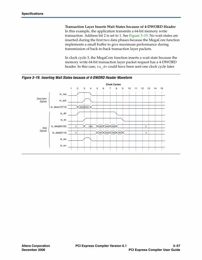
Specifications
Transaction Layer Inserts Wait States because of 4-DWORD HeaderIn this example, the application transmits a 64-bit memory write transaction. Address bit 2 is set to 1. See Figure 3–19. No wait states are inserted during the first two data phases because the MegaCore function implements a small buffer to give maximum performance during transmission of back-to-back transaction layer packets.
In clock cycle 3, the MegaCore function inserts a wait state because the memory write 64-bit transaction layer packet request has a 4-DWORD header. In this case, tx_dv could have been sent one clock cycle later.
Figure 3–19. Inserting Wait States because of 4-DWORD Header Waveform
tx_req
tx_ack
tx_desc[127:0]
tx_dfr
tx_dv
tx_data[63:32]
tx_data[31:0]
tx_ws
tx_err
DescriptorSignals
DataSignals
1 2 3 4 5 6 7 8 9 10 11 12 13 14 15
MEMWR64
Clock Cycles
X DW4DW0 DW2 DW6 X
X DW3DW1 DW5 DW7 X
Altera Corporation PCI Express Compiler Version 6.1 3–57December 2006 PCI Express Compiler User Guide

Signals
Priority Given ElsewhereIn this example, the application transmits a 64-bit memory write transaction of 8 DWORDS. Address bit 2 is set to 0. The transmit path has a 3-deep 64-bit buffer to handle back-to-back transaction layer packets as fast as possible, and it accepts the tx_desc and first tx_data without delay. See Figure 3–20.
In clock cycle 5, the MegaCore function asserts tx_ws a second time to throttle the flow of data because priority was not given immediately to this virtual channel. Priority was given to either a pending data link layer packet, a configuration completion, or another virtual channel. The tx_err is not available in the x8 MegaCore function.
Figure 3–20. 64-Bit Memory Write Request Waveform
tx_req
tx_ack
tx_desc[127:0]
tx_dfr
tx_dv
tx_data[63:32]
tx_data[31:0]
tx_ws
tx_err
DescriptorSignals
DataSignals
1 2 3 4 5 6 7 8 9 10 11 12 13 14 15
MEMWR64
Clock Cycles
X DW1 DW3 DW5 DW7 X
X DW0 DW2 DW4 DW6 X
3–58 PCI Express Compiler Version 6.1 Altera CorporationPCI Express Compiler User Guide December 2006

Specifications
Transmit Request Can Remain Asserted Between Transaction Layer PacketsIn this example, the application transmits a 64-bit memory read transaction followed by a 64-bit memory write transaction. Address bit 2 is set to 0. See Figure 3–21.
In clock cycle 4, tx_req is not deasserted between transaction layer packets.
In clock cycle 5, the second transaction layer packet is not immediately acknowledged because of additional overhead associated with a 64-bit address, such as a separate number and an LCRC. This situation leads to an extra clock cycle between two consecutive transaction layer packets.
Figure 3–21. 64-Bit Memory Read Request Waveform
tx_req
tx_ack
tx_desc[127:0]
tx_dfr
tx_dv
tx_data[63:32]
tx_data[31:0]
tx_ws
tx_err
DescriptorSignals
DataSignals
1 2 3 4 5 6 7 8 9 10 11 12 13 14 15
MEMRD64
Clock Cycles
X DW1 DW3 DW5 DW7 X
X DW0 DW2 DW4 DW6 X
MEMWR64
Altera Corporation PCI Express Compiler Version 6.1 3–59December 2006 PCI Express Compiler User Guide

Signals
Multiple Wait States Throttle Data TransmissionIn this example, the application transmits a 32-bit memory write transaction. Address bit 2 is set to 0. See Figure 3–22. No wait states are inserted during the first two data phases because the MegaCore function implements a small buffer to give maximum performance during transmission of back-to-back transaction layer packets.
In clock cycles 5, 7, 9, and 11, the MegaCore function inserts wait states to throttle the flow of transmission.
Figure 3–22. Multiple Wait States that Throttle Data Transmission Waveform
tx_req
tx_ack
tx_desc[127:0]
tx_dfr
tx_dv
tx_data[63:32]
tx_data[31:0]
tx_ws
tx_err
DescriptorSignals
DataSignals
1 2 3 4 5 6 7 8 9 10 11 12 13 14 15
MEMWR64
Clock Cycles
X DW5DW1 DW3 DW7 XDW9 DW11
X DW4DW0 DW2 DW6 XDW8 DW10
3–60 PCI Express Compiler Version 6.1 Altera CorporationPCI Express Compiler User Guide December 2006

Specifications
Error Asserted & Transmission Is NullifiedIn this example, the application transmits a 64-bit memory write transaction of 14 DWORDS. Address bit 2 is set to 0. See Figure 3–23.
In clock cycle12, tx_err is asserted which nullifies transmission of the transaction layer packet on the link. Nullified packets have the LCRC inverted from the calculated value and use the end bad packet (EDB) control character instead of the normal END control character.
Figure 3–23. Error Assertion Waveform
Receive Interface Operation Signals
The receive interface, like the transmit Interface, is based on two independent busses, one for the descriptor phase (rx_desc[135:0]) and one for the data phase (rx_data[63:0]). Every transaction includes a descriptor. A descriptor is a standard transaction layer packet header as defined by the PCI Express Base Specification Revision 1.0a with two exceptions. Bits 126 and 127 indicate the transaction layer packet group and bits 135:128 describe BAR and address decoding information (see rx_desc[135:0] below for details).
Receive Data Path Signals
Receive data path signals can be divided into two groups:
■ Descriptor phase signals■ Data phase signals
tx_req
tx_ack
tx_desc[127:0]
tx_dfr
tx_dv
tx_data[63:32]
tx_data[31:0]
tx_ws
tx_err
DescriptorSignals
DataSignals
1 2 3 4 5 6 7 8 9 10 11 12 13 14 15
MEMWR64
Clock Cycles
DW5DW1 DW3 DW7 DW9 DWB DWD DWF
DW4DW0 DW2 DW6 DW8 DWA DWC DWE
Altera Corporation PCI Express Compiler Version 6.1 3–61December 2006 PCI Express Compiler User Guide

Signals
1 In the following tables, transmit interface signal names suffixed with 0 are for virtual channel 0. If the MegaCore function implements additional virtual channels, there are an additional set of signals suffixed with the virtual channel number.
Table 3–27 describes the standard descriptor phase signals.
Table 3–27. Standard Descriptor Phase Signals (Part 1 of 2)
Signal I/O Description
rx_req0(1),(2)
O Receive request. This signal is asserted by the MegaCore function to request a packet transfer to the application interface. It is asserted when the first two DWORDS of a transaction layer packet header are valid. This signal is asserted for a minimum of two clock cycles and rx_abort, rx_retry, and rx_ack cannot be asserted at the same time as this signal. The complete descriptor is valid on the second clock cycle that this signal is asserted.
rx_descn[135:0](1),(2)
O Receive descriptor bus. Bits (125:0) have the same meaning as a standard transaction layer packet header as defined by the PCI Express Base Specification Revision 1.0a. Byte 0 of the header occupies bits 127:120 of the rx_desc bus, byte 1 of the header occupies bits 119:112, and so on, with byte 15 in bits 7:0. See Appendix B, Transaction Layer Packet Header Formats for the header formats.
For bits 135:128 (descriptor and BAR decoding), see Table 3–28. Completion transactions received by an endpoint do not have any bits asserted and must be routed to the master block in the application layer.
rx_desc[127:64] begins transmission on the same clock cycle that rx_req is asserted, allowing precoding and arbitrating to begin as quickly as possible. The other bits of rx_desc are not valid until the following clock cycle as shown in the following diagram.
Bit 126 of the descriptor indicates the type of transaction layer packet in transit:
● rx_desc[126] set to 0: transaction layer packet without data● rx_desc[126] set to 1: transaction layer packet with data
rx_req
rx_ack
rx_desc[135:128]
rx_desc[127:64]
rx_desc[63:0]
1 2 3 4 5 6
Clock Cycles
X Valid X
X Valid X
X Valid X
3–62 PCI Express Compiler Version 6.1 Altera CorporationPCI Express Compiler User Guide December 2006

Specifications
The MegaCore function generates the eight MSBs of this signal with BAR decoding information. See Table 3–28.
rx_ackn(1),(2)
I Receive acknowledge. This signal is asserted for 1 clock cycle when the application interface acknowledges the descriptor phase and starts the data phase, if any. The rx_req signal is deasserted on the following clock cycle and the rx_desc is ready for the next transmission.
rx_abortn(1),(2)
I Receive abort. This signal is asserted by the application interface if the application cannot accept the requested descriptor. In this case, the descriptor is removed from the receive buffer space, flow control credits are updated, and, if necessary, the application layer generates a completion transaction with unsupported request (UR) status on the transmit side.
rx_retryn(1),(2)
I Receive retry. The application interface asserts this signal if it is not able to accept a non-posted request. In this case, the application layer must assert rx_mask0 along with rx_retry0 so that only posted and completion transactions are presented on the receive interface for the duration of rx_mask0.
rx_maskn(1),(2)
I Receive mask (non-posted requests). This signal is used to mask all non-posted request transactions made to the application interface to present only posted and completion transactions. This signal must be asserted with rx_retry0 and deasserted when the MegaCore function can once again accept non-posted requests.
Notes for Table 3–27(1) where n is the virtual channel number; For x1 and x4, n can be 0 - 3(2) For x8, n can be 0 or 1
Table 3–27. Standard Descriptor Phase Signals (Part 2 of 2)
Signal I/O Description
Table 3–28. rx_desc[135:128]: Descriptor & BAR Decoding
Bit Type 0 Component
128 = 1: BAR 0 decoded
129 = 1: BAR 1 decoded
130 = 1: BAR 2 decoded
131 = 1: BAR 3 decoded
132 = 1: BAR 4 decoded
133 = 1: BAR 5 decoded
134 = 1: Expansion ROM decoded
135 Reserved
Altera Corporation PCI Express Compiler Version 6.1 3–63December 2006 PCI Express Compiler User Guide

Signals
Table 3–29 describes the data phase signals.
Table 3–29. Data Phase Signals (Part 1 of 2)
Signal I/O Description
rx_ben[7:0](1),(2)
O Receive byte enable. These signals qualify data on rx_data[63:0]. Each bit of the signal indicates whether the corresponding byte of data on rx_data[63:0] is valid. These signals are not available in the x8 MegaCore function.
rx_dfrn(1),(2))
O Receive data phase framing. This signal is asserted on the same or subsequent clock cycle as rx_req to request a data phase (assuming a data phase is needed). It is deasserted on the clock cycle preceding the last data phase to signal to the application layer the end of the data phase. The application layer does not need to implement a data phase counter.
rx_dvn(1),(2)
O Receive data valid. This signal is asserted by the MegaCore function to signify that rx_data[63:0] contains data.
rx_datan[63:0](1),(2)
O Receive data bus. This bus transfers data from the link to the application layer. It is 2 DWORDS wide and is naturally aligned with the address in one of two ways, depending on bit 2 of rx_desc.
● rx_desc[2] (64-bit address) set to 0: The first DWORD is located on rx_data[31:0].
● rx_desc[34] (32-bit address) set to 0: The first DWORD is located on bits rx_data[31:0].
● rx_desc[2] (64-bit address) set to 1: The first DWORD is located on bits rx_data[63:32].
● rx_desc[34] (32-bit address) set to 1: The first DWORD is located on bits rx_data[63:32].
This natural alignment allows you to connect rx_data[63:0] directly to a 64-bit data path aligned on a QW address (in the little endian convention).
Bit 2 is set to 1 (5 DWORD transaction)
Bit 2 is set to 0 (5 DWORD transaction)
rx_wsn(1),(2)
I Receive wait states. With this signal, the application layer can insert wait states to throttle data transfer.
rx_data[63:32]
rx_data[31:0]
1 2 3 4 5 6
Clock Cycles
X DW 2DW 0 XDW 4
X DW 3DW 1 X
rx_data[63:32]
rx_data[31:0]
1 2 3 4 5 6
Clock Cycles
X DW 2DW 0 XDW 4
X DW 3DW 1 X
3–64 PCI Express Compiler Version 6.1 Altera CorporationPCI Express Compiler User Guide December 2006

Specifications
Transaction Examples Using Receive Signals
This section provides additional examples that illustrate how transaction signals interact:
■ Transaction without data payload■ Retried transaction and masked non-posted transactions■ Transaction aborted■ Transaction with data payload■ Transaction with data payload and wait states
In each waveform, a strong horizontal line separates descriptor signals from data signals.
Notes for Table 3–29(1) where n is the virtual channel number; For x1 and x4, n can be 0 - 3(2) For x8, n can be 0 or 1
Table 3–29. Data Phase Signals (Part 2 of 2)
Signal I/O Description
Altera Corporation PCI Express Compiler Version 6.1 3–65December 2006 PCI Express Compiler User Guide

Signals
Transaction without Data PayloadIn Figure 3–24, the MegaCore function receives three consecutive transactions, none of which have data payloads:
■ Memory read request (64-bit addressing mode)■ Memory read request (32-bit addressing mode)■ I/O read request
In clock cycles 4, 7, and 12, the MegaCore function updates flow control credits after each transaction layer packet has either been acknowledged or aborted. When necessary, the MegaCore function generates flow control DLLPs to advertise flow control credit levels.
In clock cycle 8, the I/O read request initiated at clock cycle 8 is not acknowledged until clock cycle 11 with assertion of rx_ack. The relatively late acknowledgment could be due to possible congestion.
Figure 3–24. Three Transactions without Data Payloads Waveform
rx_req
rx_ack
rx_desc[135:128]
rx_desc[127:64]
rx_desc[63:0]
rx_abort
rx_retry
rx_mask
rx_dfr
rx_dv
rx_ws
rx_data[63:32]
rx_data[31:0]
rx_be[7:0]
DescriptorSignals
DataSignals
1 2 3 4 5 6 7 8 9 10 11 12 13 14
Clock Cycles
XX MEMRD64 MEMRD32 X I/O RD X
X
X
X
XX Valid X Valid X
XX Valid X Valid X
Valid
Valid
3–66 PCI Express Compiler Version 6.1 Altera CorporationPCI Express Compiler User Guide December 2006

Specifications
Retried Transaction & Masked Non-Posted TransactionsWhen the application layer can no longer accept non-posted requests, one of two things happen: either the application layer requests the packet be resent or it asserts rx_mask. For the duration of rx_mask, the MegaCore function masks all non-posted transactions and reprioritizes waiting transactions in favor of posted and completion transactions. When the application layer can once again accept non-posted transactions, rx_mask is deasserted and priority is given to all non-posted transactions that have accumulated in the receive buffer.
Each virtual channel has a dedicated data path and associated buffers, and no ordering relationships exist between virtual channels. While one virtual channel may be temporarily blocked, data flow continues across other virtual channels without impact. Within a virtual channel, reordering is mandatory only for non-posted transactions to prevent deadlock. Reordering is not implemented in the following cases:
■ Between traffic classes mapped in the same virtual channel■ Between posted and completion transactions■ Between transactions of the same type regardless of the relaxed-
ordering bit of the transaction layer packet
In Figure 3–25, the MegaCore function receives a memory read request transaction of 4 DWORDS that it cannot immediately accept. A second transaction (memory write transaction of 1 DWORD) is waiting in the receive buffer. Bit 2 of rx_data[63:0] for the memory write request is set to 1.
In clock cycle 3, transmission of non-posted transactions is not permitted for as long as rx_mask is asserted.
Flow control credits are updated only after a transaction layer packet has been extracted from the receive buffer and both the descriptor phase and data phase (if any) have ended. This update happens in clock cycles 8 and 12 in Figure 3–25.
Altera Corporation PCI Express Compiler Version 6.1 3–67December 2006 PCI Express Compiler User Guide

Signals
Figure 3–25. Retried Transaction & Masked Non-Posted Transaction Waveform
Transaction AbortedIn Figure 3–26, a memory read of 16 DWORDS is sent to the application layer. Having determined it will never be able to accept the transaction layer packet, the application layer discards it by asserting rx_abort. An alternative design might implement logic whereby all transaction layer packets are accepted and, after verification, potentially rejected by the application layer. An advantage of asserting rx_abort is that transaction layer packets with data payloads can be discarded in 1 clock cycle.
Having aborted the first transaction layer packet, the MegaCore function can transmit the second, a 3 DWORD completion in this case. The MegaCore function does not treat the aborted transaction layer packet as an error and updates flow control credits as if the transaction were acknowledged. In this case, the application layer is responsible for generating and transmitting a completion with completer abort status and to signal a completer abort event to the MegaCore function configuration space through assertion of cpl_err.
rx_req
rx_ack
rx_desc[135:128]
rx_desc[127:64]
rx_desc[63:0]
rx_abort
rx_retry
rx_mask
rx_dfr
rx_dv
rx_ws
rx_data[63:32]
rx_data[31:0]
rx_be[7:0]
DescriptorSignals
DataSignals
1 2 3 4 5 6 7 8 9 10 11 12 13 14
Clock Cycles
XX ValidValid X Valid X
X
XX DW 0
00h00h F0h
XX MEMWR 1DWMEMRD 4DW X MEMRD 4DW X
XX ValidValid X Valid X
3–68 PCI Express Compiler Version 6.1 Altera CorporationPCI Express Compiler User Guide December 2006

Specifications
In clock cycle 6, rx_abort is asserted and transmission of the next transaction begins on clock cycle 8.
Figure 3–26. Aborted Transaction Waveform
rx_req
rx_ack
rx_desc[135:128]
rx_desc[127:64]
rx_desc[63:0]
rx_abort
rx_retry
rx_mask
rx_dfr
rx_dv
rx_ws
rx_data[63:32]
rx_data[31:0]
rx_be[7:0]
DescriptorSignals
DataSignals
1 2 3 4 5 6 7 8 9 10 11 12 13 14
Clock Cycles
Valid X Valid X
XX DW 1
0FhX FFh X
DW 2X DW 0 X
MEMRD 16DW X CPL 3DW X
Valid X Valid X
Altera Corporation PCI Express Compiler Version 6.1 3–69December 2006 PCI Express Compiler User Guide

Signals
Transaction with Data PayloadIn Figure 3–27, the MegaCore function receives a completion transaction of 8 DWORDS and a second memory write request of 3 DWORDS. Bit 2 of rx_data[63:0] is set to 0 for the completion transaction and to 1 for the memory write request transaction.
Normally, rx_dfr is asserted on the same or following clock cycle as rx_req; however, in this case the signal is already asserted until clock cycle 7 to signal the end of transmission of the first transaction. It is immediately reasserted on clock cycle 8 to request a data phase for the second transaction.
Figure 3–27. Transaction with a Data Payload Waveform
rx_req
rx_ack
rx_desc[135:128]
rx_desc[127:64]
rx_desc[63:0]
rx_abort
rx_retry
rx_mask
rx_dfr
rx_dv
rx_ws
rx_data[63:32]
rx_data[31:0]
rx_be[7:0]
DescriptorSignals
DataSignals
1 2 3 4 5 6 7 8 9 10 11 12 13 14
Clock Cycles
ValidValid X
FFhX FFh X
DW 2X DW 0 X
X X
DW 3DW 1 DW 7DW 5 X
X DW 1 XDW 2DW 0 DW 6DW 4 X
F0h
MEMWR AD1 3DWCPLD 8DW XX X
ValidValid XX X
3–70 PCI Express Compiler Version 6.1 Altera CorporationPCI Express Compiler User Guide December 2006

Specifications
Transaction with Data Payload & Wait StatesThe application layer can assert rx_ws as often as it likes. In Figure 3–28, the MegaCore function receives a completion transaction of 4 DWORDS. Bit 2 of rx_data[63:0] is set to 1. Both the application layer and the MegaCore function insert wait states. Normally rx_data[63:0] would contain data in clock cycle 4, but the MegaCore function has inserted a wait state by deasserting rx_dv.
In clock cycle 11, data transmission does not resume until both of the following conditions are met:
■ The MegaCore function asserts rx_dv at clock cycle 10, thereby ending a MegaCore function-induced wait state.
■ The application layer deasserts rx_ws at clock cycle 11, thereby ending an application interface-induced wait state.
Figure 3–28. Transaction with a Data Payload & Wait States Waveform
rx_req
rx_ack
rx_desc[135:128]
rx_desc[127:64]
rx_desc[63:0]
rx_abort
rx_retry
rx_mask
rx_dfr
rx_dv
rx_ws
rx_data[63:32]
rx_data[31:0]
rx_be[7:0]
DescriptorSignals
DataSignals
1 2 3 4 5 6 7 8 9 10 11 12 13 14
Clock Cycles
Valid
X DW 1 X
X X
DW 3X
FFhX F0h X0FhX
DW 2X DW 0 X
CPLD 4DWX X
ValidX X
Altera Corporation PCI Express Compiler Version 6.1 3–71December 2006 PCI Express Compiler User Guide

Signals
Dependencies Between Receive Signals
Table 3–30 describes the minimum and maximum latency values in clock cycles between various receive signals.
Clocking
The Altera PCI Express MegaCore functions use one of several possible clocking configurations, depending on the PHY (generic PIPE or Stratix GX) and the reference clock frequency. The functions have two clock input signals, refclk and clk125_in.
The functions also have an output clock, clk125_out, that is a 125-MHz transceiver clock. In Stratix GX PHY implementations, clk125_out is a 125-MHz version of the transceiver reference clock and must be used to generate clk125_in. In generic PIPE PHY implementations, this signal is driven from the refclk input.
■ refclk–This signals provides the reference clock for the transceiver for Stratix GX PHY implementations. For generic PIPE PHY implementations, refclk is driven directly to clk125_out.
■ clk125_in–This signal is the clock for all of the function’s registers, except for a small portion of the receive PCS layer that is clocked by a recovered clock in Stratix GX PHY implementations. All synchronous application layer interface signals are synchronous to this clock. clk125_in must be 125 MHz and in Stratix GX PHY implementations it must be the exact same frequency as clk125_out. In generic PIPE PHY implementations, it must be connected to the pclk signal from the PHY.
1 Implementing the x4 MegaCore function in Stratix GX devices uses 4 additional clock resources for the recovered clocks on a per lane basis. The PHY layer elastic buffer uses these clocks.
Table 3–30. Minimum & Maximum Latency Values in Clock Cycles Between Receive Signals
Signal 1 Signal 2 Min Typical Max Notes
rx_req rx_ack 1 1 N
rx_req rx_dfr 0 0 0 Always asserted on the same clock cycle if a data payload is present, except when a previous data transfer is still in progress. See Figure 3–27 on page 3–70.
rx_req rx_dv 1 1-2 N Assuming data is sent.
rx_retry rx_req 1 2 N rx_req refers to the next transaction request.
3–72 PCI Express Compiler Version 6.1 Altera CorporationPCI Express Compiler User Guide December 2006

Specifications
Generic PIPE PHY Clocking Configuration
When you implement a generic PIPE PHY in the MegaCore function, you must provide a 125-MHz clock on the clk125_in input. Typically, the generic PIPE PHY provides the 125-MHz clock across the PIPE interface.
All of the function’s interfaces, including the user application interface and the PIPE interface, are synchronous to the clk125_in input. You are not required to use the refclk and clk125_out signals in this case. See Figure 3–29.
Figure 3–29. Generic PIPE PHY Clock Configuration (1)
Note to Figure 3–29:(1) User and PIPE interface signals are synchronous to clk125_in.
Stratix GX PHY, 100 MHz Reference Clock
If you implement a Stratix GX PHY with a 100-MHz reference clock, you must provide a 100-MHz clock on the refclk input. Typically, this clock is the 100-MHz PCI Express reference clock as specified by the Card Electro-Mechanical (CEM) specification.
In this configuration, the 100-MHz refclk connects to an enhanced PLL within the MegaCore function to create a 125-MHz clock for use by the Stratix GX transceiver and as the clk125_out signal. The 125-MHz clock is provided on the clk125_out signal.
You must connect clk125_out back to the clk125_in input, for example, through a distribution circuit needed in the application. All of the function’s interfaces, including the user application interface and the PIPE interface, are synchronous to the clk125_in input. See Figure 3–30.
altpcie_64b_x4_pipen1b: External PHY
refclk
clk125_in
clk125_outNot Required Not Required
clk
All Logic in MegaCore Function
125-MHz pclkfrom PIPE PHY
Altera Corporation PCI Express Compiler Version 6.1 3–73December 2006 PCI Express Compiler User Guide

Signals
Figure 3–30. Stratix GX PHY, 100 MHz Reference Clock Configuration (1)
Note to Figure 3–30:(1) User and PIPE interface signals are synchronous to clk125_in.
If you want to use other outputs of the enhanced PLL for other purposes or with different phases or frequencies, you should use the 125-MHz reference clock mode and use a 100- to 125-MHz PLL external to the MegaCore function.
Stratix GX PHY, 125 MHz Reference Clock
When implementing the Stratix GX PHY with a 125-MHz reference clock, you must provide a 125-MHz clock on the refclk input. The same clock is provided to the clk125_out signal with no delay.
You must connect clk125_out back to the clk125_in input, for example, through a distribution circuit needed in the application. All of the function’s interfaces, including the user application interface and the PIPE interface, are synchronous to the clk125_in input. See Figure 3–31.
altpcie_64b_x4_pipen1b: Stratix GX 100 MHz
refclk
clk125_in
clk125_out
clk
All Logic in MegaCore Function
100-MHz Clock Source PLL
100 -> 125
inclkrx_cruclk
tx_coreclk
ALTGXB Transceiver
3–74 PCI Express Compiler Version 6.1 Altera CorporationPCI Express Compiler User Guide December 2006

Specifications
Figure 3–31. Stratix GX PHY, 125 MHz Reference Clock Configuration (1)
Note to Figure 3–31:(1) User and PIPE interface signals are synchronous to clk125_in.
Stratix GX PHY, 156.25 MHz Reference Clock
When implementing the Stratix GX PHY with a 156.25-MHz reference clock, you must provide a 156.25-MHz clock on the refclk input. The 156.25-MHz clock goes directly to the Stratix GX transceiver. The transceiver’s coreclk_out output becomes the function’s 125-MHz clk125_out output.
You must connect clk125_out back to the clk125_in input, for example, through a distribution circuit needed in the application. All of the function’s interfaces, including the user application interface and the PIPE interface, are synchronous to the clk125_in input. See Figure 3–32.
altpcie_64b_x4_pipen1b: Stratix GX 125 MHz
refclk
clk125_in
clk125_out
clk
All Logic in MegaCore Function
125-MHz Clock Source
inclkrx_cruclk
tx_coreclk
ALTGXB Transceiver
Altera Corporation PCI Express Compiler Version 6.1 3–75December 2006 PCI Express Compiler User Guide

Signals
Figure 3–32. Stratix GX PHY, 156.25 MHz Reference Clock Configuration (1)
Note to Figure 3–32:(1) User and PIPE interface signals are synchronous to clk125_in.
Stratix II GX PHY X1 & X4 100 MHz Reference Clock
When implementing the Stratix II GX PHY in a x1 or x4 configuration, the 100 MHz clock is connected directly to the ALT2GXB transceiver. The clk125_out is driven by the output of the ALT2GXB transceiver.
The clk125_out must be connected back to the clk125_in input, possibly through any distribution circuit needed in the specific application. All of the interfaces of the function, including the user application interface and the PIPE interface are synchronous to the clk125_in input. See Figure 3–34 on page 3–78 for this clocking configuration.
altpcie_64b_x4_pipen1b: Stratix GX 156.25 MHz
refclk
clk125_in
clk125_out
clk
All Logic in MegaCore Function
156.25-MHz Clock Source inclk
rx_cruclk
tx_coreclk
ALTGXB Transceiver
coreclk_out
3–76 PCI Express Compiler Version 6.1 Altera CorporationPCI Express Compiler User Guide December 2006
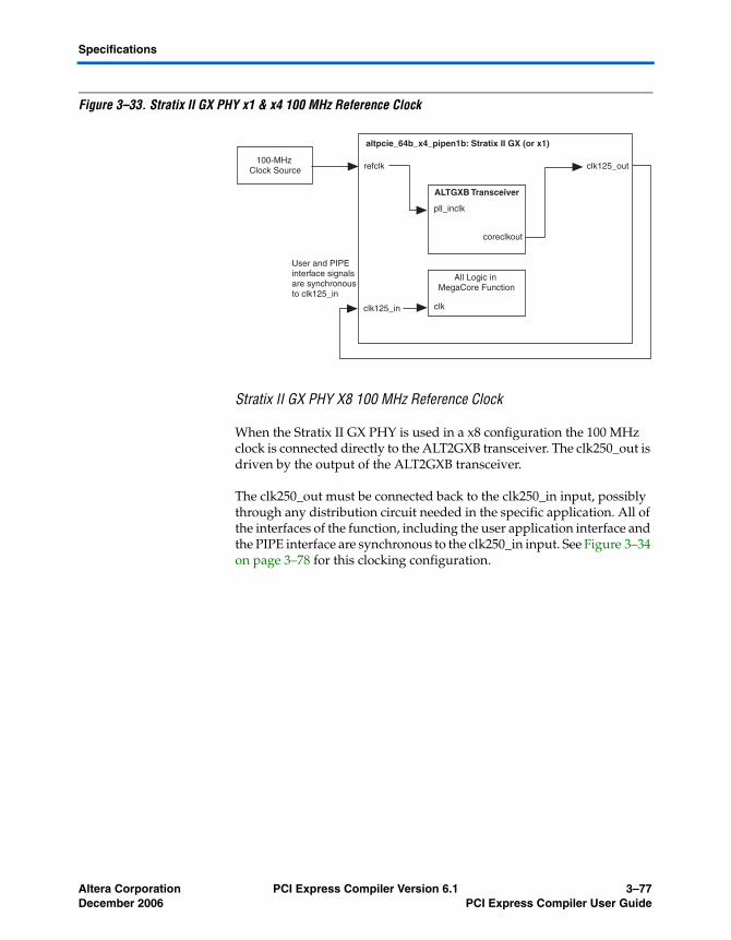
Specifications
Figure 3–33. Stratix II GX PHY x1 & x4 100 MHz Reference Clock
Stratix II GX PHY X8 100 MHz Reference Clock
When the Stratix II GX PHY is used in a x8 configuration the 100 MHz clock is connected directly to the ALT2GXB transceiver. The clk250_out is driven by the output of the ALT2GXB transceiver.
The clk250_out must be connected back to the clk250_in input, possibly through any distribution circuit needed in the specific application. All of the interfaces of the function, including the user application interface and the PIPE interface are synchronous to the clk250_in input. See Figure 3–34 on page 3–78 for this clocking configuration.
altpcie_64b_x4_pipen1b: Stratix II GX (or x1)
refclk
clk125_in
clk125_out100-MHz
Clock Source
ALTGXB Transceiver
All Logic in MegaCore Function
clk
pll_inclk
coreclkout
User and PIPE interface signalsare synchronousto clk125_in
Altera Corporation PCI Express Compiler Version 6.1 3–77December 2006 PCI Express Compiler User Guide

Signals
Figure 3–34. Stratix II GX PHY x8 100 MHz Reference Clock
Utility Signals
Refer to Figure 3–12 on page 3–44 for a diagram of all PCI Express MegaCore function signals.
Table 3–31 describes the function’s global signals.
altpcie_64b_x8_pipen1b: Stratix II GX
refclk
clk250_in
clk250_out100-MHz
Clock Source
ALTGXB Transceiver
All Logic in MegaCore Function
clk
pll_inclk
coreclkout
User and PIPE interface signalsare synchronousto clk250_in
Table 3–31. Global Signals (Part 1 of 2)
Signal I/O Description
refclk I Reference clock for the MegaCore function. It must be the frequency specified on the System Settings page accessible from the Parameter Settings tab in the MegaWizard interface. This signal is only required for Stratix GX PHY implementations. For generic PIPE implementations, this signal drives the clk125_out signal directly.
clk125_in I Input clock for the x1 and x4 MegaCore function. All of the MegaCore function I/O signals (except refclk, clk125_out, and npor) are synchronous to this clock signal. This signal must be a 125-MHz clock signal. In Stratix GX PHY implementations, the clk125_out signal can drive it, if desired. In Stratix GX PHY implementations that use a 125-MHz reference clock, the reference clock can also drive this signal. In generic PIPE implementations, the pclk supplied by the PIPE PHY device typically drives clk125_in. This signal is not on the x8 MegaCore function.
clk125_out O Output clock for the x1 and x4 MegaCore function. 125-MHz clock output derived from the refclk input in Stratix GX PHY implementations. In generic PIPE PHY implementations, the refclk input drives this signal. This signal is not on the x8 MegaCore function.
3–78 PCI Express Compiler Version 6.1 Altera CorporationPCI Express Compiler User Guide December 2006

Specifications
Figure 3–35 shows the function’s global reset signals.
clk250_in I Input clock for the x8 MegaCore function. All of the MegaCore function I/O signals (except refclk, clk250_out, and npor) are synchronous to this clock signal. This signal must be identical in frequency to the clk250_out clock signal. This signal is only on the x8 MegaCore Function.
clk250_out O Output from the x8 MegaCore function. 250-MHz clock output derived from the refclk input. This signal is only on the x8 MegaCore Function.
rstn I Asynchronous Reset of Configuration Space and Data Path Logic. Active Low. This signal is only available on the x8 MegaCore function.
npor I Power on reset. This signal is the asynchronous active-low power-on reset signal. This reset signal is used to initialize all configuration space sticky registers, PLL, and SERDES circuitry. In 100- or 156.25-MHz reference clock implementations, clk125_out is held low while npor is asserted.
srst I Synchronous data path reset. This signal is the synchronous reset of the data path state machines of the MegaCore function. It is active high. This signal is only available on the x1 and x4 MegaCore functions.
crst I Synchronous configuration reset. This signal is the synchronous reset of the nonsticky configuration space registers of the MegaCore function. It is active high. This signal is only available on the x1 and x4 MegaCore functions.
app_clk O Output clock from x1 MegaCore function to the application layer. The clock can be 125Mhz or 62.5Mhz and is derived from refclk. This signal is only on the x1Megacore function.
l2_exit O L2 exit. The PCI Express specifications define fundamental hot, warm, and cold reset states. A cold reset (assertion of crst and srst) must be performed when the LTSSM exits L2 state (signaled by assertion of this signal). This signal is active low and otherwise remains high.
hotrst_exit O Hot reset exit. This signal is asserted for 1 clock cycle when the LTSSM exists hot reset state. It informs the application layer that it is necessary to assert a global reset (crst and srst). This signal is active low and otherwise remains high.
dlup_exit O DL up exit. This signal indicates the transition from DL_UP to DL_DOWN. It is another source of internal reset and should cause the assertion of the crst and srst synchronous resets. This signal is active low.
Table 3–31. Global Signals (Part 2 of 2)
Signal I/O Description
Altera Corporation PCI Express Compiler Version 6.1 3–79December 2006 PCI Express Compiler User Guide

Signals
Figure 3–35. Global Reset Signals for x1 and x4 MegaCore Functions
The x1 and x4 MegaCore functions have three reset inputs, npor, srst, and crst. npor is used internally for all sticky registers (registers that may not be reset in L2 low power mode or by the fundamental reset). npor is typically generated by a logical OR of the power-on-reset generator and the perst signal as specified in the PCI Express card electromechanical specification.
The srst signal is a synchronous reset of the data path state machines. The crst signal is a synchronous reset of the nonsticky configuration space registers. srst and crst should be asserted whenever the l2_exit, hotrst_exit, or dlup_exit signals are asserted.
The reset block shown in Figure 3–36 is not included as part of the MegaCore function to provide some flexibility for implementation-specific methods of generating a reset.
Figure 3–35 shows the function’s global reset signals.
Figure 3–36. Global Reset Signals for x8 MegaCore Functions
Other PowerOn Reset
PCI Express x1 or x4 MegaCore
Function
perst#npor
srstcrst
l2_exithotrst_exitdlup_exit
Other PowerOn Reset
PCI Expressx8 MegaCore
Function
perst#npor
rstn
l2_exithotrst_exitdlup_exit
3–80 PCI Express Compiler Version 6.1 Altera CorporationPCI Express Compiler User Guide December 2006

Specifications
The x8 MegaCore function has two reset inputs, npor and rstn. The npor reset is used internally for all sticky registers (registers that may not be reset in L2 low power mode or by the fundamental reset). npor is typically generated by a logical OR of the power-on-reset generator and the perst signal as specified in the PCI Express card electromechanical specification.
The rstn signal is an asynchronous reset of the data path state machines and the nonsticky configuration space registers. rstn should be asserted whenever the l2_exit, hotrst_exit, or dlup_exit signals are asserted.
The reset block shown in Figure 3–36 is not included as part of the MegaCore function to provide some flexibility for implementation-specific methods of generating a reset.
Table 3–32 shows the function’s power management signals.
Table 3–32. Power Management Signals (Part 1 of 2)
Signal I/O Description
pme_to_cr I Power management turn off control register. This signal is asserted to acknowledge the PME_turn_off message by sending pme_to_ack to the root port.
pme_to_sr O Power management turn off status register. This signal is asserted when the endpoint receives the PME_turn_off message from the root port. It is asserted until pme_to_cr is asserted.
Altera Corporation PCI Express Compiler Version 6.1 3–81December 2006 PCI Express Compiler User Guide

Signals
Figure 3–37 illustrates the behavior of pme_to_sr and pme_to_cr in an endpoint. First, the MegaCore function receives the PME_turn_off message. Then, the application attempts to send the PME_to_ack message to the root port.
Figure 3–37. pme_to_sr & pme_to_cr in an Endpoint Waveform
MSI & INTx Interrupt signals
The MegaCore function supports both message signaled interrupt (MSI) and INTx interrupts. MSI transactions are write transaction layer packets.
cfg_pmcsr[31:0] O Power management capabilities register. This register is read only and provides information related to power management for a specific function.
● cfg_pmcsr[31:24]: Data register: This field indicates which power states a function can assert PME#.
● cfg_pmcsr[23:16]: Reserved.● cfg_pmcsr[15]: PME_status: When this signal is set to 1, it indicates
that the function would normally assert the PME# signal independent of the state of the PME_en bit.
● cfg_pmcsr[14:13]: Data_scale: This field indicates the scaling factor when interpreting the value retrieved from the Data register. This field is read -only.
● cfg_pmcsr[12:9]: Data_select: This field indicates which data should be reported through the Data register and the Data_scale field.
● cfg_pmcsr[8]: PME_EN: 1: indicates that the function can assert PME#0: indicates that the function cannot assert PME#
● cfg_pmcsr[7:2]: Reserved● cfg_pmcsr[1:0]: PM_STATE
Table 3–32. Power Management Signals (Part 2 of 2)
Signal I/O Description
Data Register
31 24 23 16 012789131415 12
Reserved
PME_status
Data_scale
Data_select
PME_EN
Reserved
PM_state
pme_to_sr
pme_to_cr
1 2 3 4 5 6 7 8 9 10 11 12 13 14
Clock Cycles
15
3–82 PCI Express Compiler Version 6.1 Altera CorporationPCI Express Compiler User Guide December 2006

Specifications
Table 3–33 describes MegaCore function’s interrupt signals.
Table 3–33. Interrupt Signals (Part 1 of 2)
Signal I/O Description
app_msi_req I Application MSI request. This signal is used by the application to request an MSI.
app_msi_ack O Application MSI acknowledge. This signal is sent by the MegaCore function to acknowledge the application’s request for an MSI.
app_msi_tc[2:0] I Application MSI traffic class. This signal indicates the traffic class used to send the MSI (unlike INTx interrupts, any traffic class can be used to send MSIs).
app_msi_num[4:0] I Application MSI offset number. This signal is used by the application to indicate the offset between the base message data and the MSI to send.
cfg_msicsr[15:0] O Configuration MSI control status register. This bus provides MSI software control. ● cfg_msicsr[15:9]: Reserved.● cfg_msicsr[8]: Per vector masking capable
1: function supports MSI per vector masking0: function does not support MSI per vector masking
● cfg_msicsr[7]: 64-bit address capable1: function capable of sending a 64-bit message address0: function not capable of sending a 64-bit message address
● cfg_msicsr[6:4]: Multiple message enable: This field indicates permitted values for MSI signals. For example, if “100” is written to this field 16 MSI signals are allocated.000: 1 MSI allocated001: 2 MSI allocated010: 4 MSI allocated011: 8 MSI allocated100: 16 MSI allocated101: 32 MSI allocated110: Reserved111: Reserved
● cfg_msicsr[3:1]: Multiple message capable: This field is read by system software to determine the number of requested MSI messages. 000: 1 MSI requested001: 2 MSI requested010: 4 MSI requested011: 8 MSI requested100: 16 MSI requested101: 32 MSI requested110: Reserved111: Reserved
● cfg_msicsr[0]: MSI enable: If set to 0, this component is not permitted to use MSI.
Altera Corporation PCI Express Compiler Version 6.1 3–83December 2006 PCI Express Compiler User Guide
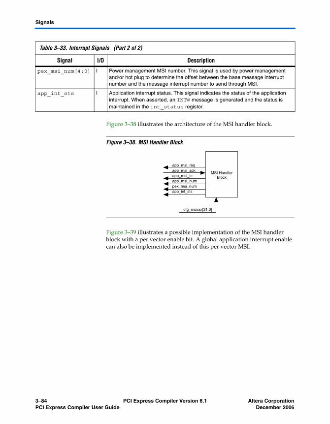
Signals
Figure 3–38 illustrates the architecture of the MSI handler block.
Figure 3–38. MSI Handler Block
Figure 3–39 illustrates a possible implementation of the MSI handler block with a per vector enable bit. A global application interrupt enable can also be implemented instead of this per vector MSI.
pex_msi_num[4:0] I Power management MSI number. This signal is used by power management and/or hot plug to determine the offset between the base message interrupt number and the message interrupt number to send through MSI.
app_int_sts I Application interrupt status. This signal indicates the status of the application interrupt. When asserted, an INT# message is generated and the status is maintained in the int_status register.
Table 3–33. Interrupt Signals (Part 2 of 2)
Signal I/O Description
MSI HandlerBlock
app_msi_reqapp_msi_ackapp_msi_tcapp_msi_numpex_msi_numapp_int_sts
cfg_msicsr[31:0]
3–84 PCI Express Compiler Version 6.1 Altera CorporationPCI Express Compiler User Guide December 2006

Specifications
Figure 3–39. Example Implementation of the MSI Handler Block
There are 32 possible MSI messages. The number of messages requested by a particular component does not necessarily correspond to the number of messages allocated. For example, in Figure 3–40, the endpoint requests eight MSI but is only allocated two. In this case, the application layer must be designed to use only two allocated messages.
Figure 3–40. MSI Request Example
app_int_en0
app_int_sts0
app_msi_req0
app_int_en1
app_int_sts1
app_msi_req1
app_int_sts
MSIArbitration
msi_enable & Master Enable
app_msi_req
app_msi_ack
Vector 1
Vector 0
R/W
R/W
Endpoint
8 Requested2 Allocated
Root Complex
RootPort
InterruptBlock
CPU
Interrupt Register
Altera Corporation PCI Express Compiler Version 6.1 3–85December 2006 PCI Express Compiler User Guide

Signals
Figure 3–41 illustrates the interactions among MSI interrupt signals for the root port in Figure 3–40. The minimum latency possible between app_msi_req and app_msi_ack is 1 clock cycle.
Figure 3–41. MSI Interrupt Signals Waveform
Table 3–34 describes 3 example implementations; one in which all 32 MSI messages are allocated and two in which only four are allocated.
MSI generated for hot plug, power management events, and system errors always use TC0. MSI generated by the application layer can use any traffic class. For example, a DMA that generates an MSI at the end of a transmission can use the same traffic control as was used to transfer data.
app_msi_req
app_msi_tc[2:0]
app_msi_num[4:0]
app_msi_ack
1 2 3 4 5 6 7 8 9 10 11 12 13
Clock Cycles
Valid
Valid
Table 3–34. MSI Messages Requested, Allocated & Mapped
MSIAllocated
32 4 4
System error 31 3 3
Hot plug and power management event 30 2 3
Application 29:0 1:0 2:0
3–86 PCI Express Compiler Version 6.1 Altera CorporationPCI Express Compiler User Guide December 2006

Specifications
.
Configuration Space Signals
The signals in Table 3–35 reflect the current values of several configuration space registers that the application layer may need to access.
Table 3–35. Configuration Space Signals
Signal I/O Description
cfg_tcvcmap[23:0] O Configuration traffic class/virtual channel mapping: The application layer uses this signal to generate a transaction layer packet mapped to the appropriate virtual channel based on the traffic class of the packet.
● cfg_tcvcmap[2:0]: Mapping for TC0 (always 0).● cfg_tcvcmap[5:3]: Mapping for TC1.● cfg_tcvcmap[8:6]: Mapping for TC2.● cfg_tcvcmap[11:9]: Mapping for TC3.● cfg_tcvcmap[14:12]: Mapping for TC4.● cfg_tcvcmap[17:15]: Mapping for TC5.● cfg_tcvcmap[20:18]: Mapping for TC6.● cfg_tcvcmap[23:21]: Mapping for TC7.
cfg_busdev[12:0] O Configuration bus device: This signal generates a transaction ID for each transactionlayer packet, and indicates the bus and device number of the MegaCore function. Because the MegaCore function only implements one function, the function numberof the transaction ID must be set to 000b.
● cfg_busdev[12:5]: Bus number.● cfg_busdev[4:0]: Device number.
cfg_prmcsr[31:0] O Configuration primary control status register. The content of this register controls thePCI status.
cfg_devcsr[31:0] O Configuration dev control status register. See PCI Express specification for details
cfg_linkcsr[31:0] O Configuration link control status register. See PCI Express specification for details.
Altera Corporation PCI Express Compiler Version 6.1 3–87December 2006 PCI Express Compiler User Guide

Signals
Completion Interface Signals
Table 3–36 shows the function’s completion interface signals.
Table 3–36. Completion Interface Signals
Signal I/O Description
cpl_err[2:0] I Completion error. This signal reports completion errors to the configuration space. The three types of errors that the application layer must report are:
● Completion time out error: cpl_err[0]: This signal must be asserted when a master-like interface has performed a non-posted request that never receives a corresponding completion transaction after the 50 ms time-out period. The MegaCore function automatically generates an error message that is sent to the root complex.
● Completer abort error: cpl_err[1]: This signal must be asserted when a target block cannot process a non-posted request. In this case, the target block generates and sends a completion packet with completer abort (CA) status to the requestor and then asserts this error signal to the MegaCore function. The block automatically generates the error message and sends it to the root complex.
● Unexpected completion error: cpl_err[2]: This signal must be asserted when a master block detects an unexpected completion transaction, i.e., no completion resource is waiting for a specific packet.
cpl_pending I Completion pending. The application layer must assert this signal when a master block is waiting for completion, i.e., a transaction is pending. If this signal is asserted and low power mode is requested, the MegaCore function waits for deassertion of this signal before transitioning into low-power state.
3–88 PCI Express Compiler Version 6.1 Altera CorporationPCI Express Compiler User Guide December 2006

Specifications
Maximum Completion Space Signals
Table 3–37 shows the maximum completion space signals.
alt2gxb Support Signals
This section describes signals alt2gxb support signals, which are only present on variants that use the Stratix II GX integrated PHY, ALT2GXB. They are connected directly to the ALT2GXB instance. In many cases these signals need to be shared with ALT2GXB instances that will be implemented in the same device. The following signals exist:
■ cal_blk_clk ■ reconfig_clk ■ reconfig_togxb■ reconfig_fromgxb
Table 3–38 describes these alt2gxb support signals.
Table 3–37. Maximum Completion Space Signals
Signal I/O Description
ko_cpl_spc_vcn[19:0]where n is 0 - 3 for the x1 and x4 cores, and 0 - 1 for the x8 core
O This static signal reflects the amount of Rx Buffer space reserved for completion headers and data. It provides the same information as what is shown in the Rx buffer space allocation table of the wizard’s Buffer Setup page (see “Buffer Setup Page” on page 3–37). The bit field assignments for this signal are:
● ko_cpl_spc_vcn[7:0] : Number of completion headers that can be stored in the Rx buffer.
● ko_cpl_spc_vcn[19:8] : Number of 16-byte completion data segments that can be stored in the Rx buffer.
The application layer logic is responsible for making sure that the completion buffer space does not overflow. It needs to limit the number and size of non-posted requests outstanding to ensure this.
Altera Corporation PCI Express Compiler Version 6.1 3–89December 2006 PCI Express Compiler User Guide

Signals
l
Physical Layer Interface Signals
This section describes signals for the three possible types of physical interfaces (1-bit, 20-bit, or PIPE). Refer to Figure 3–12 on page 3–44 for a diagram of all of the PCI Express MegaCore function signals.
Table 3–38. alt2gxb Support Signals
Signal I/O Description
cal_blk_clk I The cal_blk_clk input signal is connected to the ALT2GXB calibration block clock (cal_blk_clk) input. All instances of ALT2GXB in the same device musthave their cal_blk_clk inputs connected to the same signal because there is only one calibration block per device. This input should be connected to a clock operating as recommended by the Stratix II GX Device Handbook.
reconfig_clk I The reconfig_clk input signal is the ALT2GXB dynamic reconfiguration clock.ALT2GXB dynamic reconfiguration is not supported for PCI Express. Therefore, this signal usually can be tied low in your design. This signal is provided for casesin which the PCI Express instance shares a Stratix II GX transceiver quad with another protocol that supports dynamic reconfiguration. In these cases, this signamust be connected as described in the Stratix II GX Device Handbook.
reconfig_togxb I The reconfig_togxb[2:0] input bus is the ALT2GXB dynamic reconfigurationdata input. ALT2GXB dynamic reconfiguration is not supported for PCI Express. Therefore, this bus usually can be tied '010' in your design. This bus is provided forcases in which the PCI Express instance shares a Stratix II GX transceiver quad with another protocol that supports dynamic reconfiguration. In these cases, this signal must be connected as described in the Stratix II GX Device Handbook.
reconfig_fromgxb O The reconfig_fromgxb output signal is the ALT2GXB dynamic reconfigurationdata output. ALT2GXB dynamic reconfiguration is not supported for PCI Express.Therefore, this output signal can be left unconnected in your design. This signal isprovided for cases in which the PCI Express instance shares a Stratix II GX transceiver quad with another protocol that supports dynamic reconfiguration. In these cases, this signal must be connected as described in the Stratix II GX DeviceHandbook.
3–90 PCI Express Compiler Version 6.1 Altera CorporationPCI Express Compiler User Guide December 2006

Specifications
Serial Interface Signals
Table 3–39 describes the serial interface signals. Signals that include lane number 0 also exist for lanes 1 - 3, as marked in the table. These signals are available if you use the Stratix GX PHY or the Stratix II GX PHY.
PIPE Interface Signals
The x1 and x4 MegaCore function is compliant with the 16-bit version of the PIPE interface, enabling use of an external PHY. The x8 MegaCore function is compliant with the 8-bit version of the PIPE interface. These signals are available even when you select the Stratix GX PHY or Stratix II GX PHY so that you can simulate using both the 1-bit and the PIPE interface. Typically, simulation is much faster using the PIPE interface. See Table 3–40. Signals that include lane number 0 also exist for lanes 1-7, as marked in the table.
Table 3–39. 1-Bit Interface Signals
Signal I/O Description
tx_outnwhere n is the lane number ranging from 0-7
O Transmit input 0. This signal is the serial output of lane 0 (2.5 Gbps on differential signals).
rx_innwhere n is the lane number 0-7
I Receive input 0. This signal is the serial input of lane 0 (2.5 Gbps on differential signals).
pipe_mode I pipe_mode selects whether the MegaCore function uses the PIPE interface or the 1-bit interface. Setting pipe_mode to a 1 selects the PIPE interface, setting it to 0 selects the 1-bit interface. When simulating, you can set this signal to indicate which interface is used for the simulation. When compiling your design for an Altera device, set this signal to 0.
Altera Corporation PCI Express Compiler Version 6.1 3–91December 2006 PCI Express Compiler User Guide

Signals
Table 3–40. PIPE Interface Signals (Part 1 of 2)
Signal I/O Description
txdatan_extn[15:0](1) O Transmit data 0 (2 symbols on lane 0). This bus transmits data on lane 0. The first transmitted symbol is txdata_ext[7:0] and the second transmitted symbol is txdata0_ext[15:8]. For the x8 MegaCore
function or 8-bit PIPE mode only txdata0_ext[7:0] is available. txdatakn_ext[1:0](1)
O Transmit data control 0 (2 symbols on lane 0). This signal serves as the control bit for txdatan_ext; txdatakn_ext[0] for the first transmitted symbol and txdatakn_ext[1] for the second (8b/10b encoding). For the x8 MegaCore function or 8-bit PIPE mode only the single bit signal txdatakn_ext is available.
txdetectrxn_ext(1)
O Transmit detect receive 0. This signal is used to tell the PHY layer to start a receive detection operation or to begin loopback.
txelecidlen_ext(1)
O Transmit electrical idle 0. This signal forces the transmit output to electrical idle.
txcompln_ext(1)
O Transmit compliance 0. This signal forces the running disparity to negative in compliance mode (negative COM character).
rxpolarityn_ext(1)
O Receive polarity 0. This signal instructs the PHY layer to do a polarity inversion on the 8b/10b receiver decoding block.
powerdownn_ext[1:0](1)
O Power down 0. This signal requests the PHY to change it’s power state to the specified state (P0, P0s, P1, or P2).
rxdatan_ext[15:0](1)
I Receive data 0 (2 symbols on lane 0). This bus receives data on lane 0. The first received symbol is rxdatan_ext[7:0] and the second is rxdatan_ext[15:8]. For the x8 MegaCore function or 8 Bit PIPE mode only rxdatan_ext[7:0] is available.
rxdatakn_ext[1:0](1)
I Receive data control 0 (2 symbols on lane 0). This signal is used for separating control and data symbols. The first symbol received is aligned with rxdatakn_ext[0] and the second symbol received is aligned with rxdatan_ext[1]. For the x8 MegaCore function or 8 Bit PIPE mode only the single bit signal rxdatakn_ext is available.
rxvalidn_ext(1)
I Receive valid 0. This symbol indicates symbol lock and valid data on rxdatan_ext and rxdatakn_ext.
phystatusn_ext(1)
I PHY status 0. This signal is used to communicate completion of several PHY requests.
rxelecidlen_ext(1)
I Receive electrical idle 0. This signal forces the receive output to electrical idle.
rxstatusn_ext[2:0](1)
I Receive status 0: This signal encodes receive status and error codes for the receive data stream and receiver detection.
3–92 PCI Express Compiler Version 6.1 Altera CorporationPCI Express Compiler User Guide December 2006

Specifications
Test Signals
Table 3–40 describes the available test signals.
pipe_rstn O Asynchronous reset to external phy. It is tied high and expects a pull-down resistor on the board. During FPGA configuration, the pull-down resistor will reset the phy and after that the FPGA will drive the phy out of reset. This signal is only on MegaCore function configured for the external phy.
pipe_txclk O Transmit data path clock to external phy. This clock is derived from refclk and it provides the source synchronous clock for the transmit data of the phy.
Notes for Table 3–40(1) where n is the lane number ranging from 0-7
Table 3–40. PIPE Interface Signals (Part 2 of 2)
Signal I/O Description
Table 3–41. Test Interface Signals
Signal I/O Description
test_in[31:0] I The test_in bus provides run-time control for specific MegaCore features as well as error injection capability. See Appendix C, Test Port Interface Signals for a complete description of the individual bits in this bus. For normal operation this bus can be driven to all 0s.
test_out[511:0]for x1 or x4 test_out[127:0] for x8
O The test_out bus provides extensive monitoring of the internal state of the MegaCore function. See Appendix C, Test Port Interface Signals for a complete description of the individual bits in this bus. For normal operation this bus can be left unconnected.
Altera Corporation PCI Express Compiler Version 6.1 3–93December 2006 PCI Express Compiler User Guide

MegaCore Verification
MegaCore Verification
To ensure PCI Express compliance, Altera has performed extensive validation of the PCI Express MegaCore functions. Validation includes both simulation and hardware testing.
Simulation Environment
Altera’s verification simulation environment for the PCI Express MegaCore functions uses multiple testbenches consisting of industry-standard bus functional models driving the PCI Express link interface. A custom bus functional model connects to the application-side interface.
Altera ran the following tests in the simulation environment:
■ Directed tests that test all types and sizes of transaction layer packets and all bits of the configuration space.
■ Error injection tests that inject errors in the link, transaction layer packets, data link layer packets, and check for the proper response from the MegaCore functions.
■ PCI-SIG Compliance Checklist tests that specifically test the items in the checklist.
■ Random tests that test a wide range of traffic patterns across one or more virtual channels.
Compatibility Testing Environment
Altera has performed significant hardware testing of the PCI Express MegaCore functions to ensure a reliable solution. The MegaCore functions have been tested at various PCI-SIGs PCI Express Compliance Workshops in 2005 and 2006 with Stratix II GX and various external PHYs, and they have passed all PCI-SIG gold tests and interoperability tests with a wide selection of motherboards and test equipment. In addition, Altera internally tests every release with motherboards and switch chips from a variety of manufacturers. All PCI-SIG compliance tests are also run with each release.
3–94 PCI Express Compiler Version 6.1 Altera CorporationPCI Express Compiler User Guide December 2006

Altera Corporation PCI ExDecember 2006
4. External PHYs
External PHY Support
This chapter discusses external PHY support, which includes the new external PHYs and interface modes shown in Table 4–1.
When an external PHY is selected additional logic required to connect directly to the external PHY is included in the <variation name> module or entity.
The user logic must instantiate this module or entity in his design. The implementation details for each of these modes are discussed in the following sections.
Table 4–1. External PHY Interface Modes
PHY Interface Mode Clock Frequency Notes
16-bit SDR 125 MHz In this generic 16-bit PIPE interface, both the Tx and Rx data are clocked by the pclk from the PHY.
16-bit SDR Mode (with source synchronous transmit cock)
125 MHz This enhancement to the generic PIPE interface adds a TxClk to clock the TxData source synchronously to the External PHY. The TIXIO1100 Phy uses this mode.
8-bit DDR 125 MHz This double data rate version saves I/O pins without increasing the clock frequency. It uses a single pclk from the PHY for clocking data in both directions.
8-bit DDR Mode (with 8-bit DDR source synchronous transmit cock)
125 MHz This double data rate version saves I/O pins without increasing the clock frequency. A TxClk clocks the data source synchronously in the transmit direction. he TIXIO1100 Phy uses this mode.
8-bit SDR 250 MHz This is the generic 8-bit PIPE interface. Both the Tx and Rx data are clocked by the pclk from the PHY. The Philips PX1011APHY uses this mode.
8-bit SDR Mode (with Source Synchronous Transmit Clock)
250 MHz This enhancement to the generic PIPE interface adds a TxClk to clock the TxData source synchronously to the external PHY.
press Compiler Version 6.1 4–1

External PHY Support
16-bit SDR Mode
The implementation of this 16-bit SDR mode PHY support is shown in Figure 4–1 and is included in the file <variation name>.v or <variation name>.vhd and includes a PLL. The PLL inclock is driven by refclk and has the following 3 outputs:
1 The refclk is the same as pclk, the parallel clock provided by the external PHY. This documentations uses the terms refclk and pclk interchangeably.
■ clk125_out is a 125 MHz output that has the same phase-offset as refclk. The clk125_out must drive the clk125_in input in the user logic as shown in the Figure 4–1. The clk125_in is used to capture the incoming receive data and also is used to drive the clk125_in input of the MegaCore.
■ clk125_early is a 125 MHz output that is phase shifted. This phase-shifted output clocks the output registers of the transmit data. Based on your board delays, you may need to adjust the phase-shift of this output. To alter the phase shift, copy the PLL source file referenced in your variation file from the <path>/ip/PCI Express Compiler/lib directory to your project directory. Then use the MegaWizard Plug In Manger in the Quartus II software to edit the PLL source file to set the required phase shift. Then add the modified PLL source file to your Quartus II project.
■ tlp_clk62p5 is a 62.5 MHz output that drives the tlp_clk input of the MegaCore function when the MegaCore internal clock frequency is 62.5 MHz.
4–2 PCI Express Compiler Version 6.1 Altera CorporationPCI Express Compiler User Guide December 2006

External PHYs
Figure 4–1. 16-bit SDR Mode
16-bit SDR Mode with a Source Synchronous TxClk
The implementation of the 16-bit SDR mode with a source synchronous TxClk is shown in Figure 4–2 and is included in the file <variation name>.v or <variation name>.vhd. In this mode the following clocking scheme is used:
■ refclk is used as the clk125_in for the core
■ refclk clocks a single data rate register for the incoming receive data
■ refclk clocks the Transmit Data Register (txdata) directly
A
D
Q1
Q4
ENB
refclk
rxdata
A
D
Q 1
Q 4
ENB
txdata
125Mhz SDR Mode without txclk
A
D
Q1
Q4
ENB
PCIe IP MegaCore
Mode 1PLL tlp_clk_62p5
clk125_out
refclk clk125_out
clk125_in
clk125_in
A
D
Q1
Q4
ENB
External connection in user logic
tlp_clkclk125_early
Altera Corporation PCI Express Compiler Version 6.1 4–3December 2006 PCI Express Compiler User Guide

External PHY Support
■ refclk also clocks a DDR register that is used to create a center aligned TxClk.
This is the only external PHY mode that does not require a PLL. However, if the slow tlp_clk feature is used with this PIPE interface mode, then a PLL is required to create the slow tlp_clk. In the case of the slow tlp_clk, the circuit is similar to the one shown previously in Figure 4–1, the 16-bit SDR, but with TxClk output added.
Figure 4–2. 16-bit SDR Mode with a Source Synchronous TxClk
125Mhz 16-bit SDR Mode with txclktlp_clk @ 125Mhz
A
D
Q1
Q4
ENB
DDIO
txclk (~refclk)
A
D
Q1
Q4
ENB
refclk
rxdata
A
D
Q 1
Q 4
ENB
txdata A
D
Q1
Q4
ENB PCIe IP MegaCore
clk125_out
refclk clk125_out
ck125_in
clk125_in
External connection in user logic
tlp_clk
4–4 PCI Express Compiler Version 6.1 Altera CorporationPCI Express Compiler User Guide December 2006

External PHYs
8-bit DDR Mode
The implementation of the 8-bit DDR mode shown in Figure 4–3 is included in the file <variation name>.v or <variation name>.vhd and includes a PLL. The PLL inclock is driven by refclk (pclk from the external PHY) and has the following 3 outputs:
■ A zero delay copy of the 125 MHz refclk. The zero delay PLL output is used as the clk125_in for the core and clocks a double data rate register for the incoming receive data.
■ A 250 MHz "early" output this is multiplied from the 125 MHz refclk is early in relation to the refclk. The 250 MHz early clock PLL output is used to clock an 8-bit SDR transmit data output register. A 250 MHz single data rate register is used for the 125 MHz DDR output because this allows the use of the SDR output registers in the Cyclone II IOB. The early clock is required to meet the required clock to out times for the common refclk for the PHY. You may need to adjust the phase shift for your specific PHY and board delays. To alter the phase shift, copy the PLL source file referenced in your variation file from the <path>/ip/PCI Express Compiler/lib directory to your project directory. Then use the MegaWizard Plug In Manger in the Quartus II software to edit the PLL source file to set the required phase shift. Then add the modified PLL source file to your Quartus II project.
■ An optional 62.5 MHz TLP Slow clock is provided for x1 implementations.
An edge detect circuit is used to detect the relationships between the 125 MHz clock and the 250 MHz rising edge to properly sequence the 16-bit data into the 8-bit output register.
Altera Corporation PCI Express Compiler Version 6.1 4–5December 2006 PCI Express Compiler User Guide

External PHY Support
Figure 4–3. 8-Bit DDR Mode
8-bit DDR with a Source Synchronous TxClk
The implementation of the 8-bit DDR mode with a source synchronous transmit clock (TxClk) is shown in Figure 4-4 and is included in the file <variation name>.v or <variation name>.vhd and includes a PLL. The PLL inclock is driven by refclk (pclk from the external PHY) and has the following 3 outputs:
■ A zero delay copy of the 125 MHz refclk used as the clk125_in for the MegaCore function and also to clock DDR input registers for the Rx data and status signals.
clk125_in
rxdata
8-bit DDR without txclk
Edge Detect and Sync
0
0
0
0
0
txdata_h
txdata_l
A
D
Q1
Q4
ENB
txdata
PCIe IP MegaCore
A
D
Q1
Q4
ENB
DDIO
Mode 3PLL tlp_clk
clk250_early
clk125_out
refclk
Clk125_pll_in
clk125_out
refclk
clk125_in
Tlp_clkt
A
D
Q1
Q4
ENB
External connection in user logic
out txclk
4–6 PCI Express Compiler Version 6.1 Altera CorporationPCI Express Compiler User Guide December 2006

External PHYs
■ A 250 MHz "early" clock PLL output clocks an 8-bit SDR transmit data output register. This 250 MHz early output is multiplied from the 125 MHz refclk and is early in relation to the refclk. A 250 MHz single data rate register for the 125 MHz DDR output allows you to use the SDR output registers in the Cyclone II IOB.
■ An optional 62.5 MHz TLP Slow clock is provided for x1 implementations.
An edge detect circuit is used to detect the relationships between the 125 MHz clock and the 250 MHz rising edge to properly sequence the 16-bit data into the 8-bit output register.
Figure 4–4. 8-bit DDR Mode with a Source Synchronous Transmit Clock
clk125_in
rxdata
8-bit DDR Mode with txclk
Edge Detect and Sync
0
0
0
0
0
txdata_h
txdata_l
A
D
Q 1
Q 4
ENB
txdata
A
D
Q 1
Q 4
ENB
txclk
PCIe IP MegaCore
A
D
Q1
Q4
ENB
DDIO
Mode 3PLL tlp_clk
clk250_early
clk125_out
pclk
clk125_out
refclk
clk125_in
tlp_clk
A
D
Q 1
Q 4
ENB
External connection in user logic
Altera Corporation PCI Express Compiler Version 6.1 4–7December 2006 PCI Express Compiler User Guide

External PHY Support
8-bit SDR Mode
The implementation of the 8-bit SDR mode is shown in Figure 4–5 and is included in the file <variation name>.v or <variation name>.vhd and includes a PLL. The PLL inclock is driven by refclk (pclk from the external PHY) and has the following 3 outputs:
■ A 125 MHz output derived from the 250 MHz refclk used as the clk125_in for the core and also to transition the incoming 8-bit data into a 16-bit register for the rest of the logic.
■ A 250 MHz "early" output that is skewed early in relation to the refclk that is used to clock an 8-bit SDR transmit data output register. The early clock PLL output is used to clock the transmit data output register. The early clock is required to meet the required clock to out times for the common clock. You may need to adjust the phase shift for your specific PHY and board delays. To alter the phase shift, copy the PLL source file referenced in your variation file from the <path>/ip/PCI Express Compiler/lib directory to your project directory. Then use the MegaWizard Plug In Manger in the Quartus II software to edit the PLL source file to set the required phase shift. Then add the modified PLL source file to your Quartus II project.
■ An optional 62.5 MHz TLP Slow clock is provided for x1 implementations.
An edge detect circuit is used to detect the relationships between the 125 MHz clock and the 250 MHz rising edge to properly sequence the 16-bit data into the 8-bit output register.
4–8 PCI Express Compiler Version 6.1 Altera CorporationPCI Express Compiler User Guide December 2006

External PHYs
Figure 4–5. 8-bit SDR Mode
8-bit SDR with a Source Synchronous TxClk
The implementation of the 16-bit SDR mode with a source synchronous TxClk is shown in Figure 4–6 and is included in the file <variation name>.v or <variation name>.vhd and includes a PLL. The PLL inclock is driven by refclk (pclk from the external PHY) and has the following 3 outputs:
■ A 125 MHz output derived from the 250 MHz refclk. This 125 MHz PLL output is used as the clk125_in for the MegaCore function.
■ A 250 MHz "early" output that is skewed early in relation to the refclk the 250 MHz early clock PLL output is used to clock an 8-bit SDR transmit data output register.
clk125_in
A
D
Q1
Q4
ENB
refclk (250 Mhz)
rxdata
250Mhz SDR Mode
Edge Detect and Sync
0
0
0
0
0
txdata_h
txdata_l
A
D
Q1
Q4
ENB
txdata
PCIe IP MegaCore
A
D
Q1
Q4
ENB
A
D
Q1
Q4
ENB
rxdata_h
rxdata_l
Mode 4PLL
tlp_clk
clk250_early
clk125_out
A
D
Q1
Q4
ENB
A
D
Q1
Q4
ENB
A
D
Q1
Q4
ENB
clk125_in
tlp_clk
refclkExternal connection in user logic
Altera Corporation PCI Express Compiler Version 6.1 4–9December 2006 PCI Express Compiler User Guide
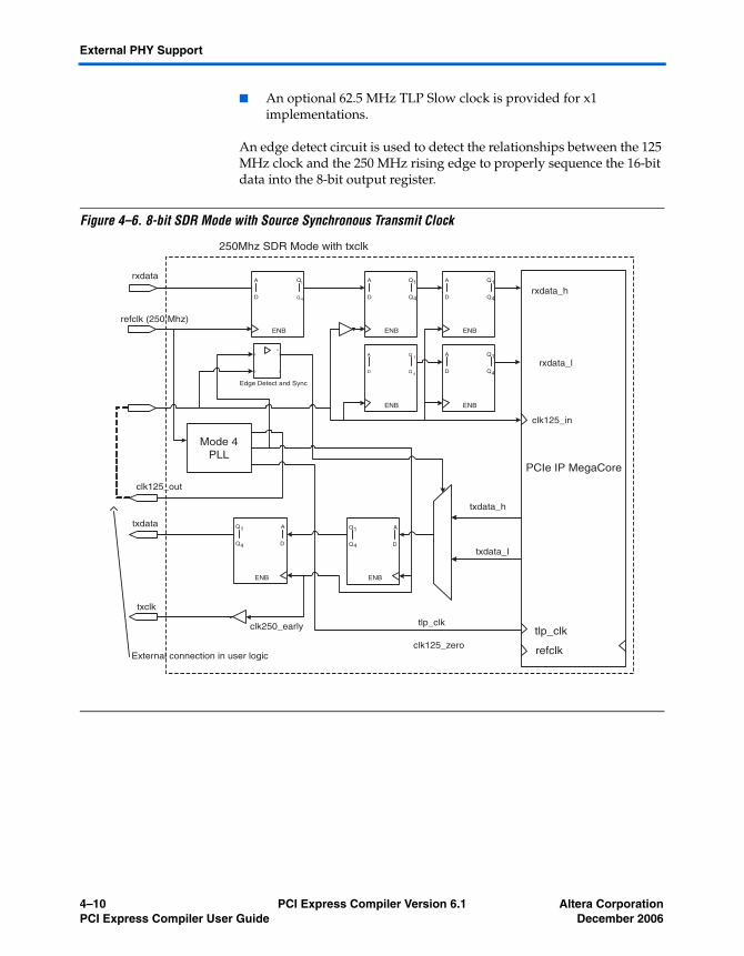
External PHY Support
■ An optional 62.5 MHz TLP Slow clock is provided for x1 implementations.
An edge detect circuit is used to detect the relationships between the 125 MHz clock and the 250 MHz rising edge to properly sequence the 16-bit data into the 8-bit output register.
Figure 4–6. 8-bit SDR Mode with Source Synchronous Transmit Clock
A
D
Q1
Q4
ENB
refclk (250 Mhz)
rxdata
250Mhz SDR Mode with txclk
Edge Detect and Sync
0
0
0
0
0
txdata_h
txdata_l
A
D
Q1
Q4
ENB
txdata
txclk
PCIe IP MegaCore
A
D
Q1
Q4
ENB
A
D
Q 1
Q 4
ENB
rxdata_h
rxdata_l
Mode 4PLL
clk125_zero
tlp_clkclk250_early
clk125_out
A
D
Q1
Q4
ENB
A
D
Q1
Q4
ENB
A
D
Q1
Q4
ENB
External connection in user logic
clk125_in
refclk
tlp_clk
4–10 PCI Express Compiler Version 6.1 Altera CorporationPCI Express Compiler User Guide December 2006

External PHYs
16-bit PHY Interface Signals
The external I/O signals for the 16-bit PIPE Interface Modes are summarized in Table 4–2. Depending on the number of lanes selected and whether the PHY mode has a TxClk, some of the signals may not be available as noted.
Table 4–2. 16-bit PHY Interface Signals (Part 1 of 2)
Signal Name Direction Description Availability
pcie_rstn I PCI Express Reset signal, active low. Always
phystatus_ext I PIPE Interface phystatus signal. PHY is signaling completion of the requested operation
Always
powerdown_ext[1:0] O PIPE Interface powerdown signal, requests the PHY to enter the specified power state.
Always
refclk I Input clock connected to the PIPE Interface pclk signal from the PHY. 125 MHz clock used to clock all of the status and data signals
Always
pipe_txclk O Source synchronous transmit cock signal for clocking Tx Data and Control signals going to the PHY.
Only in modes that have the TxClk
rxdata0_ext[15:0] I PIPE Interface Lane 0 Rx Data signals, carries the parallel received data.
Always
rxdatak0_ext[1:0] I PIPE Interface Lane 0 Rx Data K-character flags. Always
rxelecidle0_ext I PIPE Interface Lane 0 Rx Electrical Idle Indication.
Always
rxpolarity0_ext O PIPE Interface Lane 0 Rx Polarity Inversion Control
Always
rxstatus0_ext[1:0] I PIPE Interface Lane 0 Rx Status flags. Always
rxvalid0_ext I PIPE Interface Lane 0 Rx Valid indication Always
txcompl0_ext O PIPE Interface Lane 0 Tx Compliance control Always
txdata0_ext[15:0] O PIPE Interface Lane 0 Tx Data signals, carries the parallel transmit data.
Always
txdatak0_ext[1:0] O PIPE Interface Lane 0 Tx Data K-character flags. Always
txelecidle0_ext O PIPE Interface Lane 0 Tx Electrical Idle Control Always
rxdata1_ext[15:0] I PIPE Interface Lane 1 Rx Data signals, carries the parallel received data.
Only in x4
rxdatak1_ext[1:0] I PIPE Interface Lane 1 Rx Data K-character flags. Only in x4
rxelecidle1_ext I PIPE Interface Lane 1 Rx Electrical Idle Indication.
Only in x4
rxpolarity1_ext O PIPE Interface Lane 1 Rx Polarity Inversion Control
Only in x4
Altera Corporation PCI Express Compiler Version 6.1 4–11December 2006 PCI Express Compiler User Guide

External PHY Support
rxstatus1_ext[1:0] I PIPE Interface Lane 1 Rx Status flags. Only in x4
rxvalid1_ext I PIPE Interface Lane 1 Rx Valid indication Only in x4
txcompl1_ext O PIPE Interface Lane 1 Tx Compliance control Only in x4
txdata1_ext[15:0] O PIPE Interface Lane 1 Tx Data signals, carries the parallel transmit data.
Only in x4
txdatak1_ext[1:0] O PIPE Interface Lane 1 Tx Data K-character flags. Only in x4
txelecidle1_ext O PIPE Interface Lane 1 Tx Electrical Idle Control Only in x4
rxdata2_ext[15:0] I PIPE Interface Lane 2 Rx Data signals, carries the parallel received data.
Only in x4
rxdatak2_ext[1:0] I PIPE Interface Lane 2 Rx Data K-character flags. Only in x4
rxelecidle2_ext I PIPE Interface Lane 2 Rx Electrical Idle Indication.
Only in x4
rxpolarity2_ext O PIPE Interface Lane 2 Rx Polarity Inversion Control
Only in x4
rxstatus2_ext[1:0] I PIPE Interface Lane 2 Rx Status flags. Only in x4
rxvalid2_ext I PIPE Interface Lane 2 Rx Valid indication Only in x4
txcompl2_ext O PIPE Interface Lane 2 Tx Compliance control Only in x4
txdata2_ext[15:0] O PIPE Interface Lane 2 Tx Data signals, carries the parallel transmit data.
Only in x4
txdatak2_ext[1:0] O PIPE Interface Lane 2 Tx Data K-character flags. Only in x4
txelecidle2_ext O PIPE Interface Lane 2 Tx Electrical Idle Control Only in x4
rxdata3_ext[15:0] I PIPE Interface Lane 3 Rx Data signals, carries the parallel received data.
Only in x4
rxdatak3_ext[1:0] I PIPE Interface Lane 3 Rx Data K-character flags. Only in x4
rxelecidle3_ext I PIPE Interface Lane 3 Rx Electrical Idle Indication.
Only in x4
rxpolarity3_ext O PIPE Interface Lane 3 Rx Polarity Inversion Control
Only in x4
rxstatus3_ext[1:0] I PIPE Interface Lane 3 Rx Status flags. Only in x4
rxvalid3_ext I PIPE Interface Lane 3 Rx Valid indication Only in x4
txcompl3_ext O PIPE Interface Lane 3 Tx Compliance control Only in x4
txdata3_ext[15:0] O PIPE Interface Lane 3 Tx Data signals, carries the parallel transmit data.
Only in x4
txdatak3_ext[1:0] O PIPE Interface Lane 3 Tx Data K-character flags. Only in x4
txelecidle3_ext O PIPE Interface Lane 3 Tx Electrical Idle Control Only in x4
Table 4–2. 16-bit PHY Interface Signals (Part 2 of 2)
Signal Name Direction Description Availability
4–12 PCI Express Compiler Version 6.1 Altera CorporationPCI Express Compiler User Guide December 2006

External PHYs
8-bit PHY Interface Signals
The external I/O signals for the 8-bit PIPE Interface Modes are summarized in Table 4–3. Depending on the number of lanes selected and whether the PHY mode has a TxClk, some of the signals may not be available as noted.
Table 4–3. 8-bit PHY Interface Signals (Part 1 of 2)
Signal Name Direction Description Availability
pcie_rstn I PCI Express Reset signal, active low. Always
phystatus_ext I PIPE Interface phystatus signal. PHY is signaling completion of the requested operation
Always
powerdown_ext[1:0] O PIPE Interface powerdown signal, requests the PHY to enter the specified power state.
Always
refclk I Input clock connected to the PIPE Interface pclk signal from the PHY. Used to clock all of the status and data signals. Depending on whether this is an SDR or DDR interface this clock will be either 250 MHz or 125 MHz.
Always
pipe_txclk O Source synchronous transmit cock signal for clocking Tx Data and Control signals going to the PHY.
Only in modes that have the TxClk
rxdata0_ext[7:0] I PIPE Interface Lane 0 Rx Data signals, carries the parallel received data.
Always
rxdatak0_ext I PIPE Interface Lane 0 Rx Data K-character flag. Always
rxelecidle0_ext I PIPE Interface Lane 0 Rx Electrical Idle Indication. Always
rxpolarity0_ext O PIPE Interface Lane 0 Rx Polarity Inversion Control Always
rxstatus0_ext[1:0] I PIPE Interface Lane 0 Rx Status flags. Always
rxvalid0_ext I PIPE Interface Lane 0 Rx Valid indication Always
txcompl0_ext O PIPE Interface Lane 0 Tx Compliance control Always
txdata0_ext[7:0] O PIPE Interface Lane 0 Tx Data signals, carries the parallel transmit data.
Always
txdatak0_ext O PIPE Interface Lane 0 Tx Data K-character flag. Always
txelecidle0_ext O PIPE Interface Lane 0 Tx Electrical Idle Control Always
rxdata1_ext[7:0] I PIPE Interface Lane 1 Rx Data signals, carries the parallel received data.
Only in x4
rxdatak1_ext I PIPE Interface Lane 1 Rx Data K-character flag. Only in x4
rxelecidle1_ext I PIPE Interface Lane 1 Rx Electrical Idle Indication. Only in x4
rxpolarity1_ext O PIPE Interface Lane 1 Rx Polarity Inversion Control Only in x4
rxstatus1_ext[1:0] I PIPE Interface Lane 1 Rx Status flags. Only in x4
rxvalid1_ext I PIPE Interface Lane 1 Rx Valid indication Only in x4
Altera Corporation PCI Express Compiler Version 6.1 4–13December 2006 PCI Express Compiler User Guide

External PHY Support
txcompl1_ext O PIPE Interface Lane 1 Tx Compliance control Only in x4
txdata1_ext[7:0] O PIPE Interface Lane 1 Tx Data signals, carries the parallel transmit data.
Only in x4
txdatak1_ext O PIPE Interface Lane 1 Tx Data K-character flag. Only in x4
txelecidle1_ext O PIPE Interface Lane 1 Tx Electrical Idle Control Only in x4
rxdata2_ext[7:0] I PIPE Interface Lane 2 Rx Data signals, carries the parallel received data.
Only in x4
rxdatak2_ext I PIPE Interface Lane 2 Rx Data K-character flag. Only in x4
rxelecidle2_ext I PIPE Interface Lane 2 Rx Electrical Idle Indication. Only in x4
rxpolarity2_ext O PIPE Interface Lane 2 Rx Polarity Inversion Control Only in x4
rxstatus2_ext[1:0] I PIPE Interface Lane 2 Rx Status flags. Only in x4
rxvalid2_ext I PIPE Interface Lane 2 Rx Valid indication Only in x4
txcompl2_ext O PIPE Interface Lane 2 Tx Compliance control Only in x4
txdata2_ext[7:0] O PIPE Interface Lane 2 Tx Data signals, carries the parallel transmit data.
Only in x4
txdatak2_ext O PIPE Interface Lane 2 Tx Data K-character flag. Only in x4
txelecidle2_ext O PIPE Interface Lane 2 Tx Electrical Idle Control Only in x4
rxdata3_ext[7:0] I PIPE Interface Lane 3 Rx Data signals, carries the parallel received data.
Only in x4
rxdatak3_ext I PIPE Interface Lane 3 Rx Data K-character flag. Only in x4
rxelecidle3_ext I PIPE Interface Lane 3 Rx Electrical Idle Indication. Only in x4
rxpolarity3_ext O PIPE Interface Lane 3 Rx Polarity Inversion Control Only in x4
rxstatus3_ext[1:0] I PIPE Interface Lane 3 Rx Status flags. Only in x4
rxvalid3_ext I PIPE Interface Lane 3 Rx Valid indication Only in x4
txcompl3_ext O PIPE Interface Lane 3 Tx Compliance control Only in x4
txdata3_ext[7:0] O PIPE Interface Lane 3 Tx Data signals, carries the parallel transmit data.
Only in x4
txdatak3_ext O PIPE Interface Lane 3 Tx Data K-character flag. Only in x4
txelecidle3_ext O PIPE Interface Lane 3 Tx Electrical Idle Control Only in x4
Table 4–3. 8-bit PHY Interface Signals (Part 2 of 2)
Signal Name Direction Description Availability
4–14 PCI Express Compiler Version 6.1 Altera CorporationPCI Express Compiler User Guide December 2006

External PHYs
Selecting an External PHY
From the Systems Setting page which displays during the parameterization process, you select an external PHY. You have two choices:
■ Select the exact PHY ■ Select the type of interface to the PHY. Several PHYs have multiple
interface modes.
By selecting the Custom option, you can select any of the supported interfaces. Figure 4–4 shows Systems Setting Page from which you select the external PHY.
Figure 4–7. Selecting an External PHY During Parameterization
Altera Corporation PCI Express Compiler Version 6.1 4–15December 2006 PCI Express Compiler User Guide

External PHY Constraint Support
Table 4–4 summarizes the PHY support matrix. For every supported PHY Type and Interface, the table lists the allowed lane widths.
The TI XIO1100 device has some additional control signals that need to be driven by your design. These can be statically pulled high or low in the board design, unless additional flexibility is needed by your design and you want to drive them from the Altera device. These signals are:
■ P1_SLEEP must be pulled low. The PCI Express MegaCore function requires the refclk (RX_CLK from the XIO1100) to remain active while in the P1 powerdown state.
■ DDR_EN must be pulled high if your variation of the PCI Express MegaCore function uses the 8-bit DDR (w/TxClk) mode. It must be pulled low if the 16-bit SDR (w/TxClk) mode is used.
■ CLK_SEL must be set correctly based on the reference clock provided to the XIO1100. Consult the XIO1100 data sheet for specific recommendations.
External PHY Constraint Support
PCI Express Compiler supports constraints. When you parameterize and generate your MegaCore, Quartus II software creates a Tcl file that you run when run compile your design. The Tcl files incorporates the following constraints that you specify when you parameterize and generate your MegaCore function:
■ pclk frequency constraint (125 MHz or 250 Mhz)■ Setup and Hold constraints for the input signals■ Clock to out constraints for the output signals■ I/O Interface Standard
1 For more information on using the adding the constraint file when you compile your design, refer to “Compile the Design” on page 2–15.
Table 4–4. External PHY Support Matrix
PHY Type Allowed Interfaces and Lanes
16-bit SDR(pclk only)
16-bit SDR(w/TxClk)
8-bit DDR(pclk only)
8-bit DDR(w/TxClk)
8-bit SDR(pclk only)
8-bit SDR(w/TxClk)
SerialInterface
Stratix GX - - - - - - x1, x4
Stratix II GX - - - - - - x1, x4, x8
TI XIO1100 - x1 - x1 - - -
Philips PX1011A - - - - - x1 -
Custom x1, x4 x1, x4 x1, x4 x1, x4 x1, x4 x1, x4 -
4–16 PCI Express Compiler Version 6.1 Altera CorporationPCI Express Compiler User Guide December 2006

External PHYs
Using External PHYs With the Stratix GX Device Family
If you will be using an external PHY with a design that will be implemented in the Stratix GX device family, you must modify the PLL instance required by some external PHYs to work in the Stratix GX family. If you are using the Stratix GX internal PHY this is not necessary.
To modify the PLL instance, follow these steps:
1. Copy the PLL source file referenced in your variation file from the <path>/ip/PCI Express Compiler/lib directory to your project directory.
2. Use the MegaWizard Plug In Manger in the Quartus II software to edit the PLL to use the Stratix GX device family.
3. Add the modified PLL source file to your Quartus II project.
Altera Corporation PCI Express Compiler Version 6.1 4–17December 2006 PCI Express Compiler User Guide

External PHY Constraint Support
4–18 PCI Express Compiler Version 6.1 Altera CorporationPCI Express Compiler User Guide December 2006

Altera Corporation PCI ExDecember 2006
5. Testbench &Example Designs
This chapter introduces the PCI Express MegaCore function testbench, the BFM test driver module, and two example designs:
■ A simple DMA example design
■ A chaining DMA example design
After reviewing the components and the concepts in this chapter, you will have the information that you need to modify the BFM test driver module to exercise and test your own application layer design.
When you create a MegaCore function variation as described in “Generate Files” on page 2–11, an example design and testbench, customized to your variation also is generated.
The testbench instantiates an example design and a root port BFM, which provides the following configuration routine and interface:
■ A configuration routine that sets up all the basic configuration registers in the endpoint. This allows the endpoint application to be the target of and initiate PCI Express transactions.
■ A VHDL/Verilog HDL procedure interface to initiate PCI Express transactions to the endpoint.
The testbench uses test driver modules (altpcietb_bfm_driver for the simple DMA design and altpcietb_bfm_driver_chaining for the chaining DMA design) to exercise the example design’s target memory and DMA channel. This test driver module also displays information from the endpoint’s configuration space registers which lets you verify the parameters you specified in the MegaWizard interface.
Using one of the provided example designs as a sample, you can easily modify the testbench test driver module to use your own application layer design instead of the provided example design’s application layer logic. The testbench and root port BFM design simplifies the process of exercising the application layer logic that interfaces to the MegaCore function endpoint variation. PCI Express link monitoring and error injection capabilities are limited to those provided by the MegaCore function’s test_in and test_out signals. The following sections describe the testbench, two example designs, and root BFM in detail.
press Compiler Version 6.1 5–1

The Altera testbench and root port BFM provide a simple method to do basic testing of the application layer logic that interfaces to the MegaCore function endpoint variation. However, the testbench and root port BFM are not intended to be a substitute for a full verification environment. To thoroughly test your application, Altera suggests that you obtain commercially available PCI Express verification IP and tools, and/or do your own extensive hardware testing.
Your application layer design may need to handle at least the following scenarios that are not possible to create with the Altera testbench and the root port BFM. The Altera root port BFM has the following limitations:
■ It is unable to generate or receive vendor defined messages. Some systems generate vendor defined messages and the application layer must be designed to process them. The MegaCore function passes these messages on to the application layer which in most cases should ignore them, but in all cases must issue an rx_ack to clear the message from the Rx buffer.
■ It can only handle received read requests that are less than or equal to the currently set max payload size. Many systems are capable of handling larger read requests that are then returned in multiple completions.
■ It always returns a single completion for every read request. Some systems split completions on every 64-byte address boundary.
■ It always returns completions in the same order the read requests were issued. Some systems will generate the completions out of order.
■ It is unable to generate zero-length read requests that some systems generate as flush requests following some write transactions. The application layer must be capable of generating the completions to the zero length read requests.
The simple and chaining DMA example designs provided with the core are designed to handle all of the above behaviors, even though the provided testbench cannot test them.
Additionally PCI Express link monitoring and error injection capabilities are limited to those provided by the MegaCore function’s test_in and test_out signals. The testbench and root port BFM will not NAK any transactions.
5–2 PCI Express Compiler Version 6.1 Altera CorporationPCI Express Compiler User Guide December 2006

Testbench & Example Designs
Testbench The MegaWizard interface provides the Testbench in the subdirectory <variation name>_examples/simple_dma/testbench for the simple DMA design example and <variation name>_examples/chaining_dma/testbench for the chaining DMA design example in your project directory. The testbench top level is named <variation name>_testbench for the simple DMA example design, and <variation name>_chaining_testbench for the chaining DMA example design.
This testbench allows the simulation of up to an eight-lane PCI Express link using either the PIPE interfaces of the root port and endpoints or the serial PCI Express interface. See Figure 5–1 for a high level view of the testbench.
Figure 5–1. Testbench Top-Level Module: <variation name>_testbench
The top-level of the testbench instantiates four main modules:
■ <variation name>_example_pipen1b —This is the example endpoint design that includes your variation of the MegaCore function. For more information about this module, see “Simple DMA Example Design” on page 5–5.
■ altpcietb_bfm_rp_top_x8_pipen1b —This is the root port PCI Express bus functional model (BFM). For detailed information about this module, see “Root Port BFM” on page 5–27.
■ altpcietb_pipe_phy —There are eight instances of this module, one per lane. These modules interconnect the PIPE MAC layer interfaces of the root port and the endpoint. The module mimics the behavior of the PIPE PHY layer to both MAC interfaces.
Testbench Top Level (<variation name>_testbench)
Endpoint Example Design<variation name>_example_pipen1b
PIPE InterconnectionModule (x8)
(altpcierd_pipe_phy)
Root Port BFM(altpcierd_bfm_rp_top_x8_pipen1b)
Test Driver Module(altpcietb_bfm_driver)
Test Driver Module(altpcietb_bfm_driver_chaining)
Simple DMAChaining DMA
Altera Corporation PCI Express Compiler Version 6.1 5–3December 2006 PCI Express Compiler User Guide

Testbench
■ altpcietb_bfm_driver—This module drives transactions to the root port BFM. This is the module that you modify to vary the transactions sent to the example endpoint design or your own design. For more information about this module, see “BFM Test Driver Module For Simple DMA Example Design” on page 5–20.
In addition, the testbench has routines that perform the following tasks:
● Generate the reference clock for the endpoint at the required frequency
● Provide a PCI Express reset at start up.
The testbench has several VHDL generics/Verilog HDL parameters that control the overall operation of the testbench. These generics are described in Table 5–1.
Table 5–1. Testbench VHDL Generics /Verilog HDL Parameters
Generic/Parameter Allowed Values
Default Value
Description
PIPE_MODE 0 or 1 1 Controls whether the PIPE interface (PIPE_MODE = 1) or serial interface (PIPE_MODE = 0) is used for the simulation. The PIPE interface typically simulates much faster than the serial interface. If the variation name file only implements the PIPE interface, then setting PIPE_MODE to 0 has no effect and the PIPE interface always is used.
NUM_CONNECTED_LANES 1,2,4,8 8 This controls how many lanes are interconnected by the testbench. Setting this generic value to a lower number simulates the endpoint operating on a narrower PCI Express interface than the maximum.
If your variation only implements the x1 MegaCore function, then this setting has no effect and only one lane is used.
FAST_COUNTERS 0 or 1 1 Setting this parameter to a 1 speeds up simulation by making many of the timing counters in the PCI Express MegaCore function operate faster than specified in the PCI Express specification.This should usually be set to 1, but can be set to 0 if there is a need to simulate the true time-out values.
5–4 PCI Express Compiler Version 6.1 Altera CorporationPCI Express Compiler User Guide December 2006

Testbench & Example Designs
Simple DMA Example Design
This example design shows how to create an endpoint application layer design that interfaces to the PCI Express MegaCore function. The design includes the following:
■ Memory that can be a target for PCI Express memory read and write transactions.
■ A DMA channel that can initiate memory read and write transactions on the PCI Express link.
The example endpoint design is completely contained within a supported Altera device and relies on no other hardware interface than the PCI Express link. This allows you to use the example design for the initial hardware validation of your system.
The Quartus II software generates the example design in the same language that you used for the variation (generated by the variation name file); the example design is either Verilog HDL or VHDL.
When the MegaWizard interface generates the MegaCore variant, the example endpoint design is created with the MegaCore function variation. The example design includes two main components, the MegaCore function variation and an application layer example design as shown in “Top-Level Simple DMA Example Design for Simulation” on page 5–6.
The example endpoint design application layer provides these features:
■ Shows you how to interface to the PCI Express MegaCore function■ Target memory that can be written to and read from PCI Express
memory write and read transactions■ DMA channel that can be used to initiate memory read and write
transactions on the PCI Express link■ Master memory block that can be used to source and sink data for
DMA initiated memory transactions■ Data pattern generator that can be used to source data for DMA
initiated memory write transactions■ Support for two virtual channels (VCs)
The example endpoint design can be used in the testbench simulation and to compile a complete design for an Altera device. All of the modules necessary to implement the example design with the variation file are contained in separate files, based on the language you use:
<variation name>_example_top.vhd <variation name>_example_top.v altpcierd_dprambe.v or altpcierd_dprambe.vhd
Altera Corporation PCI Express Compiler Version 6.1 5–5December 2006 PCI Express Compiler User Guide

Simple DMA Example Design
altpcierd_example_app.v or altpcierd_example_app.vhdaltpcierd_master.v or altpcierd_master.vhdaltpcierd_slave.v or altpcierd_slave.vhd<variation name>_example_pipen1b.v or <variation name>_example_pipen1b. vhd<variation name>_example_top.v or <variation name>_example_top.vhd
This file is created in the project directory of the generated the MegaCore function. See “Generate Files” on page 2–11 for more information.
Figure 5–2 shows the high level block diagram of the simple DMA example endpoint design.
Figure 5–2. Top-Level Simple DMA Example Design for Simulation
The following modules are included in the example design:
■ <variation name>_example_pipen1b. This module is the top level of the example endpoint design that you use for simulation.
This module provides both PIPE and serial interfaces for the simulation environment. This module has two debug ports named test_out and test_in (see Appendix C) which allows you to monitor and control internal states of the MegaCore function.
For synthesis the top level module is <variation name>_example_top. This module instantiates the module <variation name>_example_pipen1b and propagates only a small sub-set of the test ports to the external I/Os. These test ports can be used in your design.
Master Module(altpcierd_master)
Includes DMA, Memory & Data Generator
Traffic Class to Virtual Channel
Mapping
Simple DMA Example Design Simulation Top Level (<variation name>_example_pipenb)
Slave Module(altpcierd_slave)
Includes Memory &Control Registers
Simple DMA Example Application Layer (altpcierd_example_app)
PCI Express MegaCoreFunction Variation
PHY Support Module (<variation name>)
VC0 Tx
VC0 Rx
VC1 Tx
VC1 Rx
5–6 PCI Express Compiler Version 6.1 Altera CorporationPCI Express Compiler User Guide December 2006

Testbench & Example Designs
■ <variation name>.vhd or <variation name>.v— This file instantiates the <variation name>_core entity (or module) that is described elsewhere in this section and includes additional logic required to support the specific PHY you have chosen for your variation. You should include this file when you compile your design in the Quartus II software.
■ <variation name>_core.v or <variation name>_core.vhd —This variation name module is created by MegaWizard interface during the generate phase, based on the parameters that you set when you parameterize the MegaCore function (see “Parameterize” on page 2–5). For simulation purposes, the IP functional simulation model produced by Quartus II software is used. The IP functional simulation model is either the <variation name>_core.vho or <variation name>_core.vo file. The associated <variation name>_core.vhd or <variation name>_core.v file is used by the Quartus II software during compilation. For information on producing a functional simulation model, see “Set Up Simulation” on page 2–9.
■ altpcierd_example_app —This example application layer design contains the master and slave modules. It also includes Traffic Class (TC) to Virtual Channel (VC) mapping logic that maps requests as specified by the mapping tables in the MegaCore functions configuration space. For more information, see Table 3–35 on page 3–87
■ altpcierd_slave —The slave module handles all memory read and write transactions received from the PCI Express link. Depending on which Base Address Register (BAR) the transaction matched, the transaction is directed either to the target memory or the control register space. For more information on the BAR and address mapping, see “Example Design BAR/Address Map”. For any read transactions received, the slave module generates the required completion and passes it to the MegaCore function for transmission.
■ altpcierd_master —This is the master module that includes the following functions:
● DMA channel that generates memory read and write transactions on the PCI Express link.
● Master memory block that can be the source of data for memory write transactions initiated by the DMA channel and the sink of data for memory read transactions.
Altera Corporation PCI Express Compiler Version 6.1 5–7December 2006 PCI Express Compiler User Guide

Simple DMA Example Design
● Data generator function that can alternatively be the source of data for memory write transactions initiated by the DMA channel.
For more information on setting up the DMA channel and registers, including the base address registers (BARs) for controlling the DMA channel, see the following section, “Example Design BAR/Address Map”.
Example Design BAR/Address Map
The example design maps received memory transactions to either the target memory block or the control register block based on which BAR the transaction matched. There are multiple BARs that map to each of these blocks to maximize interoperability with different variation files. Table 5–2 shows the mapping.
The example design control register block is used primarily to set up DMA channel operations. The control register block sets the addresses, size, and attributes of the DMA channel operation. Executing a DMA channel operation includes the following steps:
1. Writing the PCI Express address to the registers at offset 0x00 and 0x04.
2. Writing the master memory block address to the register at offset 0x14.
3. Writing the length of the requested operation to the register at offset 0x08.
Table 5–2. Example Design BAR Map
Memory BAR Mapping
32-bit BAR032-bit BAR164-bit BAR1:0
Maps to 32-KByte target memory block. Lower address bits select the RAM locations to be read and written. Address bits 15 and above are ignored.
32-bit BAR232-bit BAR364-bit BAR3:2
Maps to control register block. For details, see Table 5–3 Example Design Control Registers.
32-bit BAR432-bit BAR564-bit BAR5:4
Maps to 32-KByte target memory block. Lower address bits select the RAM locations to be read and written. Address bits 15 and above are ignored.
Expansion ROM BAR Not implemented by Example Design; behavior is unpredictable.
I/O Space BAR (any) Not implemented by Example Design; behavior is unpredictable.
5–8 PCI Express Compiler Version 6.1 Altera CorporationPCI Express Compiler User Guide December 2006

Testbench & Example Designs
4. Writing the attributes (including PCI Express memory write or read direction) of the requested operation to the register at offset 0x0C. Writing to this register starts the execution of the DMA channel operation.
5. Reading the DMA channel operation in progress bit at offset 0x0C to determine when the DMA channel operation has completed.
Table 5–3. Example Design Control Registers (Part 1 of 2)
Register Byte Address
(offset from BAR2,3)
Bit Field Description
0x00 31:0 DMA channel PCI Express address[31:0] —These are the lower 32 bits of the starting address used for memory transactions created by the DMA channel.
0x04 31:0 DMA channel PCI Express Address[63:32] —These are the upper 32 bits of the starting address used for memory transactions created by the DMA channel.
0x08 31:0 DMA channel operation size — This register specifies the length in bytes of the DMA operation to perform.
0x0C All DMA channel control register. Writing to any byte in this register starts a DMA operation.
31 DMA channel operation in progress —This is the read-only bit. When this bit is set to 1 a DMA operation is in progress.
30:23 Reserved.
22 DMA channel uses an incrementing DWORD pattern for memory write transactions.
21 DMA channel uses an incrementing byte pattern for memory write transactions.
20 DMA channel uses all zeros as the data for memory write transactions.
19 Reserved.
0x0C 18:16 Specifies the maximum payload size for DMA channel transactions — This can be used to restrict the DMA channel to using smaller transactions than allowed by the configuration space Max Payload Size and Max Read Request Size. The transaction size is the smallest allowed. This uses the same encoding as those fields:
000—128 Bytes001—256 Bytes010—512 Bytes 011—1 KBytes100—2 KBytes
15 Sets value of the TD bit in all PCI Express request headers generated by this DMA channel operation. The TD bit is the TLP digest field present bit.
14 Sets value of the EP bit in all PCI Express request headers generated by this DMA channel operation. The EP bit is the poisoned data bit.
Altera Corporation PCI Express Compiler Version 6.1 5–9December 2006 PCI Express Compiler User Guide

Simple DMA Example Design
0x0C 13 Sets the value of the Relaxed Ordering Attribute bit in all PCI Express request headers generated by this DMA channel operation.
12 Sets the value of the No Snoop Attribute bit in all PCI Express request headers generated by this DMA channel operation.
11 Reserved.
10:8 Sets the value of the Traffic Class field in all PCI Express request headers generated by this DMA channel operation.
7 Reserved.
6:5 Sets the value of the Packet Format Field in all PCI Express request headers generated by this DMA channel operation. The encoding is as follows:
00b—Memory read (3DW w/o data)01b—Memory read (4DW w/o data)10b—Memory write (3DW w/data)11b—Memory write (4DW w/data)
4:0 Sets the value of the Type field in all PCI Express request headers generated by this DMA channel operation. The supported encoding is:00000b—Memory read or write
0x10 31:15 Reserved
14:12 MSI Traffic Class, when requesting an MSI. Write to this field to specify which PCI-Express Traffic Class to send the MSI memory write packet.
11:9 Reserved
8:4 MSI Number, when requesting and MSI. Write to this field to specify which MSI should be sent.
3:1 Reserved
0 Interrupt Request. If MSI is enabled in the endpoint (EP) design, then writing to this bit sends a Message Signaled Interrupt (MSI). Otherwise, MSI is disabled in the EP, and so a Legacy Interrupt message is sent.
0x14 31:15 Reserved.
14:3 Starting master memory block address for the DMA channel operation.
2:0 Bits 2:0 of the starting master memory block address are copied from the starting PCI Express address.
Table 5–3. Example Design Control Registers (Part 2 of 2)
Register Byte Address
(offset from BAR2,3)
Bit Field Description
5–10 PCI Express Compiler Version 6.1 Altera CorporationPCI Express Compiler User Guide December 2006

Testbench & Example Designs
Chaining DMA Example Design
This example design shows how to create a chaining DMA endpoint in which two DMA modules support simultaneous DMA read and write transactions. One DMA module implements write operations on the upstream flow from Endpoint (EP) memory to Root Complex (RC) memory, and the other DMA implements read operations on the downstream flow from RC memory to EP memory.
The chaining DMA example design endpoint design is completely contained within a supported Altera device and relies on no other hardware interface than the PCI Express link. This allows you to use the example design for the initial hardware validation of your system.
The MegaWizard interface generates the example design in the same language that you used for the variation (generated by the variation name file); the example design is either Verilog HDL or VHDL. The chaining DMA design example requires that BAR 2 or BAR 3 is set to a minimum of 256 bytes.
During the generate step, the example endpoint design is created with the MegaCore function variation. The example design includes two main components:
■ The MegaCore function variation
■ An application layer example design
In the simple DMA example design, the software application (on the root port side) needs to program the end point DMA registers for every transfer of a given block of memories. This can introduce a performance limitation when transferring a large amount of noncontiguous memory between the BFM shared memory and the Endpoint buffer memory. The chaining DMA example design shows an architecture which is capable of transferring a large amount of fragmented memory without reprogramming the DMA registers for every memory block.
The chaining DMA example design uses descriptor tables for each block of memory to be transferred. Each descriptor table contains the following information
■ Length of the transfer■ Address of the source■ Address of the destination■ Control bits to set the handshaking behavior between the software
application and the chaining DMA module.
Altera Corporation PCI Express Compiler Version 6.1 5–11December 2006 PCI Express Compiler User Guide

Chaining DMA Example Design
The software application writes these descriptor tables in the BFM shared memory. The chaining DMA design engine continuously collects these descriptor tables for DMA read and/or DMA write. At the beginning of the transfer, the software application programs the DMA engine registers with the descriptor table header. The descriptor table header contains information such as total number of descriptor and BFM shared memory address of the first descriptor table. When the descriptor header is set, the chaining DMA engine continuously fetches descriptors from the BFM shared memory for both DMA reads and DMA writes, and then performs the data transfer for each descriptor.
Figure 5–3 shows a block diagram of the example design on the left and an external RC CPU on the left. The block diagram contains the following elements:
■ EP DMA write and read requester modules, mentioned just above.
■ An EP read/write MUX to arbitrate access to the EP memory over an Avalon®-MM bus.
■ An EP Transaction Layer Packet (TLP) translator module used to perform TLP formatting as well as traffic management to and from the appropriate submodule (DMA read or write configuration).
■ Two Root Complex (RC) memory descriptor tables, one for each DMA module. These are described in the following section.
■ An RC CPU and associated PCI Express PHY link to the EP example design, using a Root Port and a North/South Bridge.
5–12 PCI Express Compiler Version 6.1 Altera CorporationPCI Express Compiler User Guide December 2006

Testbench & Example Designs
Figure 5–3. Top-Level Chaining DMA Example for Simulation
The example endpoint design application layer has these features:
■ Shows you how to interface to the PCI Express MegaCore function
■ Provides a chaining DMA channel that can be used to initiate memory read and write transactions on the PCI Express link
You can use the example endpoint design in the testbench simulation and compile a complete design for an Altera device. All of the modules necessary to implement the example design with the variation file are contained in one of the following files, based on the language you use:
<variation name>_examples/chaining_dma/<variation name>_example_chaining.vhd or<variation name>_examples/chaining_dma/<variation name>_example_chaining.v
This file is created in the project directory when files are generated.
The following modules are included in the example design and located in the subdirectory <variation name>_example/chaining_dma:
CPU
RC Slave
Root Complex Chaining DMA Example
Endpoint Memory
Avalon-MM buses
Root Port
SS
MemoryReadDescriptorTable
WriteDescriptorTable
Data
PCI Express MegaCore Function
Variation (DUT)
MM
DMA WriteRequester
Descriptor
Header Register
DMA ReadRequester
Descriptor
Header Register
Altera Corporation PCI Express Compiler Version 6.1 5–13December 2006 PCI Express Compiler User Guide

Chaining DMA Example Design
■ <variation name>_example_pipen1b—This module is the top level of the example endpoint design that you use for simulation. This module is contained in the following files produced by the MegaWizard interface:
<variation name>_example_chaining_top.vhd
<variation name>_example_chaining_top.v
This module provides both PIPE and serial interfaces for the simulation environment. This module has two debug ports named test_out and test_in (see Appendix C, ) which allows you to monitor and control internal states of the MegaCore function.
For synthesis the top level module is <variation name>_example_chaining_top. This module instantiates the module <variation name>_example_pipen1b and propagates only a small sub-set of the test ports to the external I/Os. These test ports can be used in your design.
■ <variation name>v or <variation name>vhd —This variation name module is created by the MegaWizard interface when files are generated based on the parameters that you set. For simulation purposes, the IP functional simulation model produced by the MegaWizard interface is used. The IP functional simulation model is either the <variation name>.vho or <variation name>.vo file. The associated <variation name>.vhd or <variation name>.v file is used by the Quartus II software during compilation. For information on producing a functional simulation model, see the Getting Started chapter.
The chaining DMA example design hierarchy consists of these components:
● A DMA read and a DMA Write module
● On chip EP memory (Avalon slave) which uses two Avalon-MM buses for each engine
● RC Slave module for performance monitoring and single DWORD Mrd/Mwr
Each DMA modules consists of these components:
● Header Register module: RC programs the descriptor header (4 DWORDS) at the beginning of the DMA
5–14 PCI Express Compiler Version 6.1 Altera CorporationPCI Express Compiler User Guide December 2006

Testbench & Example Designs
● Descriptor module: DMA engine collects chaining descriptors from EP memory
● Requester module: For a given descriptor, the DMA engine performs the memory transfer between EP memory and BFM shared memory
The following modules reflect each hierarchical level:
● altpcierd_example_app_chaining —This module is the top level which arbitrates PCI Express packets for the modules altpcie_dma_dt (read or write) and altpcie_rc_slave. altpcierd_example_app_chaining instantiates the Endpoint memory used for the DMA read and write transfer
altpcie_rc_slave — is used by the software application (Root Port) to retrieve the DMA Performance counter values and performs single DWORD read and write to the Endpoint memory by bypassing the DMA engine. By default, this module is disabled.
● altpcie_dma_dt — arbitrates PCI Express packets issued by the submodules the modules altpcie_dma_prg_reg, altpcie_read_dma_requester, altpcie_write_dma_requester and altpcie_dma_descriptor
● altpcie_dma_prg_reg — contains the descriptor header table registers which get programmed by the software application. This module collects PCI Express TL packets from the software application with the tlp type MWr on BAR 2 or 3
● altpcie_dma_descriptor— retrieves DMA read or write descriptor from the root port memory, and store it in a descriptor FIFO. This module issues PCI Express TL packets to the BFM shared memory with the tlp type MRd
● altpcie_read_dma_requester—For each descriptor located in the altpcie_descriptor FIFO, this module transfer data from the BFM shared memory to the Endpoint memory by issuing MRd PCI Express TL packets
● altpcie_write_dma_requester—For each descriptor located in the altpcie_descriptor FIFO, this module transfer data from the Endpoint memory to the BFM shared memory to the by issuing MWr PCI Express TL packets
Altera Corporation PCI Express Compiler Version 6.1 5–15December 2006 PCI Express Compiler User Guide

Chaining DMA Example Design
Example Design BAR/Address Map
The example design maps received memory transactions to either the target memory block or the control register block based on which BAR the transaction matched. There are multiple BARs that map to each of these blocks to maximize interoperability with different variation files. Table 5–4 shows the mapping.
The example design control register block is used primarily to set up DMA channel operations. The control register block sets the addresses, size, and attributes of the DMA channel operation. Executing a DMA channel operation includes the following steps:
1. Writing the PCI Express address to the registers at offset 0x00 and 0x04.
2. Writing the master memory block address to the register at offset 0x14.
3. Writing the length of the requested operation to the register at offset 0x08.
4. Writing the attributes (including PCI Express memory write or read direction) of the requested operation to the register at offset 0x0C. Writing to this register starts the execution of the DMA channel operation.
5. Reading the DMA channel operation in progress bit at offset 0x0C to determine when the DMA channel operation has completed.
Table 5–4. Example Design BAR Map
Memory BAR Mapping
32-bit BAR032-bit BAR164-bit BAR1:0
Maps to 32-KByte target memory block. Use the rc_slave module to bypass the chaining DMA
32-bit BAR232-bit BAR364-bit BAR3:2
Maps to control DMA Read and DMA write register header, requires a minimum of 256 bytes.
32-bit BAR432-bit BAR564-bit BAR5:4
Maps to 32-KByte target memory block. Use the rc_slave module to bypass the chaining DMA
Expansion ROM BAR Not implemented by Example Design; behavior is unpredictable.
I/O Space BAR (any) Not implemented by Example Design; behavior is unpredictable.
5–16 PCI Express Compiler Version 6.1 Altera CorporationPCI Express Compiler User Guide December 2006

Testbench & Example Designs
Chaining DMA Descriptor Tables
Each descriptor table consists of a descriptor header at a base address, followed by a contiguous list of descriptors. Each subsequent descriptor consists of a minimum of four DWORDs (PCI-Express 32 bit double word) of data, and corresponds to one DMA transfer. The software application writes the descriptor header in the EP point Header Descriptor register. Tables 5–5, 5–6, and , describe each of the fields of this header.
Table 5–5. Chaining DMA Descriptor Header Format Address Map
Table 5–6. Chaining DMA Descriptor Header Format (Control Fields)
31 16 15 0
Control Fields (see Table 5–6) Size
BDT Upper DWORD
BDT Lower DWORD
Reserved RCLAST
31 30 28 27 25 24 20 19 18 17 16
Reserved MSI Traffic Class
Reserved MSI Number Reserved EPLAST_ENA MSI Direction
Table 5–7. Chaining DMA Descriptor Header Fields (Part 1 of 2)
Descriptor Header Field
EP Access
RC Access EP Address Description
Size R R/W 0x00 (DMA write) 0x10 (DMA read)
Specifies the number n of the descriptor in the descriptor table.
Direction R R/W 0x00 (DMA write) 0x10 (DMA read)
Specifies the DMA module to the descriptor table mapping rules. When this bit is set the descriptor table refers to the DMA write logic. When this bit is cleared the descriptor table refers to the DMA read logic.
Message Signaled Interrupt(MSI)
R R/W 0x00 (DMA write) 0x10 (DMA read)
Enables interrupts across all descriptors. When this bit is set the EP DMA module issues an interrupt using MSI to the RC. Your software application can use this interrupt to monitor the DMA transfer status.
Altera Corporation PCI Express Compiler Version 6.1 5–17December 2006 PCI Express Compiler User Guide

Chaining DMA Example Design
MSI Number R R/W 0x00 (DMA write) 0x10 (DMA read)
When your RC reads the MSI capabilities of the EP, these register bits map to the PCI Express back-end MSI signals app_msi_num [4:0].If there is more than one MSI, the default mapping if all the MSIs are available, is:MSI 0 = ReadMSI 1 = Write
MSI Traffic Class
R R/W 0x00 (DMA write) 0x10 (DMA read)
When the RC application software reads the MSI capabilities of the EP, this value is assigned by default to MSI traffic class 0. These register bits map to the PCI Express back-end signal app_msi_tc [2:0}
BDT Upper DWORD
R R/W 0x04 (DMA write) 0x14 (DMA read)
Base Address Descriptor table address
BDT Lower DWORD
R R/W 0x08 (DMA write) 0x18 (DMA read)
Base Address Descriptor table address
EPLAST_ENA R R/W 0x00 (DMA write) 0x10 (DMA read)
Enables EPLAST logic across all descriptors Enables memory polling across all descriptors. When this bit is set, the EP DMA module issues a memory write to the BFM shared memory to report the number of DMA descriptors completed. Your software application can poll this memory location to monitor the DMA transfer status.
RCLAST R R/W 0x0C (DMA write) 0x1C (DMA read)
RCLAST reflects the number of descriptors ready to be transferred. Your software application can periodically update this register based on system level memory scheduling constraints.
Table 5–7. Chaining DMA Descriptor Header Fields (Part 2 of 2)
Descriptor Header Field
EP Access
RC Access EP Address Description
5–18 PCI Express Compiler Version 6.1 Altera CorporationPCI Express Compiler User Guide December 2006

Testbench & Example Designs
See Table 5–8 for the format of the descriptor fields following the descriptor header. Each descriptor provides the hardware information on one DMA transfer. Table describes each descriptor field.
Tables 5–8, 5–9, are related to the list of descriptor tables which resides on the BFM shared memory.
Table 5–8. Chaining DMA Descriptor Format Map
Table 5–9. Chaining DMA Descriptor Format Map (Control Fields)
31 22 21 16 15 0
Reserved Control Fields (see Table 5–9) DMA Length
EP Address
RC Address Upper DWORD
RC Address Lower DWORD
21 20 19 18 17 16
Reserved Reserved Reserved MSI EPLAST_ENA
Table 5–10. Chaining DMA Descriptor Fields
Descriptor Field EP Access RC Access Description
EP Address R R/W A 32-bit field that specifies the base address of the memory transfer on the EP site.
RC AddressUpper DWORD
R R/W Specifies the upper base address of the memory transfer on the RC site.
RC Address Lower DWORD
R R/W Specifies the lower base address of the memory transfer on the RC site.
DMA Length R R/W Specifies the number of DMA bytes to transfer.
EPLAST_ENA R R/W This bit is OR’d with the EPLAST_ENA bit of the descriptor header. When EPLAST_ENA is set the EP DMA module updates the EPLast RC memory register with the value of the last completed descriptor, in the form 0 – n.
MSI R R/W This bit is OR’d with the MSI bit of the descriptor header. When this bit is set the EP module sends an interrupt completion message at the end of the DMA transfer of each channel.
Altera Corporation PCI Express Compiler Version 6.1 5–19December 2006 PCI Express Compiler User Guide

Test Driver Modules
Test Driver Modules
This section describes the test driver modules used to test the example designs:
■ “BFM Test Driver Module For Simple DMA Example Design”■ “BFM Test Driver Module for Chaining DMA Example Design”
BFM Test Driver Module For Simple DMA Example Design
The BFM driver module generated by the MegaWizard interface during the generate step is configured to test the simple DMA example endpoint design. The BFM driver module configures the endpoint configuration space registers and then tests the example endpoint design target memory and DMA channel.
For a VHDL version of this file, see: <variation name>_example_simple_dma/altpcietb_bfm_driver.vhd
or
For a Verilog HDL file, see: <variation name>_example_simple_dma/altpcietb_bfm_driver.v
The BFM test driver module performs the following steps in sequence:
1. Configures the root port and endpoint configuration spaces, which the BFM test driver module does by calling the procedure ebfm_cfg_rp_ep, which is part of altpcierd_bfm_configure.
2. Finds a suitable BAR to use for accessing the example endpoint design target memory space. One of the BARs 0, 1, 4, or 5 must be at least a 4KB memory BAR to perform the target memory test. Procedure find_mem_bar contained in the altpcietb_bfm_driver does this.
3. If a suitable BAR is found in the previous step, the target_mem_test procedure in the altpcietb_bfm_driver tests the example endpoint design target memory space. This procedure executes the following sub-steps:
a. Sets up a 4,096 byte data pattern in the BFM shared memory, which is done by a call to the shemem_fill procedure in altpcietb_bfm_shmem.
b. Writes those 4,096 bytes to the example endpoint design target memory, which is done by a call to the ebfm_barwr procedure in altpcietb_bfm_rdwr.
5–20 PCI Express Compiler Version 6.1 Altera CorporationPCI Express Compiler User Guide December 2006

Testbench & Example Designs
c. Reads the same 4,096 bytes from the target memory to a separate location in the BFM shared memory, which is done by a call to the ebfm_barrd_wait procedure in altpcietb_bfm_rdwr. This procedure blocks (waits) until the completion has been received for the read.
d. The data read back from the target memory is checked to ensure the data is the same as what was initially written, which is done by a call to the shmem_chk_ok procedure in the altpcietb_bfm_shmem.
4. Finds a suitable BAR to access the example endpoint design control register space. One of the BARs 2 or 3 must be at least a 128 byte memory BAR to perform the DMA channel test. The find_mem_bar procedure in the altpcietb_bfm_driver does this.
5. If a suitable BAR is found in the previous step, the example endpoint design DMA channel is tested by the procedure target_dma_test in the altpcietb_bfm_driver. This procedure executes the following substeps:
a. Sets up a 4,096 byte data pattern in the BFM shared memory, which is done by a call to the shemem_fill procedure in altpcietb_bfm_shmem.
b. Sets up the DMA channel control registers and starts the DMA channel to transfer data from BFM shared memory to the master memory in the example design. This is done by a series of calls to the ebfm_barwr_imm procedure in altpcietb_bfm_rdwr. The last of these ebfm_barwr_imm calls starts the DMA channel.
c. Waits for the DMA channel to finish by checking the DMA channel in-progress bit in the control register space until it is clear. This is done by a loop around the call to the ebfm_barrd_wait procedure in altpcietb_bfm_rdwr.
d. Sets up the DMA channel control registers and starts the DMA channel to transfer data back from the example design master memory to the BFM shared memory. This is done by a series of calls to the ebfm_barwr_imm procedure in altpcietb_bfm_rdwr. The last of these ebfm_barwr_imm calls starts the DMA channel.
Altera Corporation PCI Express Compiler Version 6.1 5–21December 2006 PCI Express Compiler User Guide

Test Driver Modules
e. Waits for the DMA channel to finish by checking the DMA channel in-progress bit in the control register space until it is clear. This is done by a loop around the call to the ebfm_barrd_wait procedure in altpcietb_bfm_rdwr.
f. Checks the data transferred back from the master memory by the DMA channel to ensure the data is the same as the data that was initially written. This is done by a call to the shmem_chk_ok procedure in altpcietb_bfm_shmem.
6. If a suitable BAR was found for the DMA channel test, the BFM attempts the legacy interrupt test:
a. Checks to see if the endpoint supports legacy interrupts. If so the test proceeds, otherwise the test finishes.
b. Checks the MSI message control register to see if the MSI is disabled. If MSI is enable, then the test disables MSI.
c. Sets a watchdog timer and writes to the endpoint register to trigger a legacy interrupt.
d. Waits to receive a legacy interrupt or until the watchdog timer expires.
e. Reports the results of the test, restores the value of the MSI message control register, and clears the interrupt bit in the EP.
7. If a suitable BAR was found for the legacy interrupt test, the BFM attempts the MSI interrupt test:
a. Checks the MSI capabilities register to see how many MSI registers are supported.
b. Initializes the MSI capabilities structure with the target MSI address, data, and number of messages granted to the EP.
c. Checks each MSI number by triggering the MSI in the endpoint, then polling the BFM shared memory for an interrupt from the EP. The test then loops through all MSIs that the EP supports. The test next checks that each MSI is received before the watchdog timer expires, and that the MSI data received is correct.
d. Restores the MSI control register to the pre-test state, and reports the results of the test.
5–22 PCI Express Compiler Version 6.1 Altera CorporationPCI Express Compiler User Guide December 2006

Testbench & Example Designs
e. The simulation is stopped by calling the procedure ebfm_log_stop_sim in altpcieb_bfm_log.
BFM Test Driver Module for Chaining DMA Example Design
The BFM driver module generated by the MegaWizard interface during the generate step is configured to test the chain DMA example endpoint design. The BFM driver module configures the endpoint configuration space registers and then tests the example endpoint chaining DMA channel.
For a VHDL version of this file, see: <variation name>_example_chaining_dma/testbench/<variation name>_altpcietb_bfm_driver_chaining.vhd
For a Verilog HDL file, see: <variation name>_example_chaining_dma/testbench/<variation name>_altpcietb_bfm_driver_chaining.v
The BFM test driver module performs the following steps in sequence:
1. Configures the root port and endpoint configuration spaces, which the BFM test driver module does by calling the procedure ebfm_cfg_rp_ep, which is part of altpcierd_bfm_configure.
2. Finds a suitable BAR to access the example endpoint design control register space. One of BARs, 2 or 3, must be at least a 128 byte memory BAR to perform the DMA channel test. The find_mem_bar procedure in the altpcietb_bfm_driver_chaining does this.
3. If a suitable BAR is found in the previous step, the example endpoint design chaining DMA is tested by the procedure chained_dma_test in the altpcietb_bfm_driver. This procedure is a wrapper which calls the procedures dma_wr_test and dma_rd_test for respectively DMA write and DMA read, based on the value of the direction argument.
DMA Write Cycles
The procedure dma_wr_test used for DMA writes uses the following steps:
1. Configure the BFM shared memory. This is done with three descriptors tables with the content shown below:
Altera Corporation PCI Express Compiler Version 6.1 5–23December 2006 PCI Express Compiler User Guide

Test Driver Modules
Table 5–11. Write Descriptor 0
Write Descriptor 0
Offset in BFM shared memory. Value Description
DW0 0x810 64 Transfer length in DWORDS and control bits (as described in table 5.7)
DW1 0x814 0 End Point Address value
DW2 0x818 0 BFM shared memory upper address value
DW3 0x81c 0x1800 BFM shared memory lower address value
Data 0x1800 Increment from 0xAAA0_FFFF
Data content in the BFM shared memory from address: 0x01800 0x1840
Table 5–12. Write Descriptor 1
Write Descriptor 1
Offset in BFM Shared Memory Value Description
DW0 0x820 32 Transfer length in DWORDS and control bits (as described in Table on page 5–19)
DW1 0x824 0 End Point Address value
DW2 0x828 0 BFM shared memory upper address value
DW3 0x82c 0x2800 BFM shared memory lower address value
Data 0x02800 Increment from 0xBBB0_FFFF
Data content in the BFM shared memory from address: 0x02800 0x2820
Table 5–13. Write Descriptor 2
Write Descriptor 2
Offset in BFM Shared Memory Value Description
DW0 0x830 96 Transfer length in DWORDS and control bits (as described in table 5.7)
DW1 0x834 0 End Point Address value
DW2 0x838 0 BFM shared memory upper address value
DW3 0x83c 0x04800 BFM shared memory lower address value
Data 0x04800 Increment from 0xCCC0_FFFF
Data content in the BFM shared memory from address: 0x04800 0x4860
5–24 PCI Express Compiler Version 6.1 Altera CorporationPCI Express Compiler User Guide December 2006

Testbench & Example Designs
2. Set up the chaining DMA descriptor header and starts the transfer data from the EP memory to the BFM shared memory. This is done by a call to the procedure dma_set_header which writes the following four DWORDS into the DMA write register module:
After writing the last DWORD of the Descriptor header (DW3), the DMA write starts the three subsequent data transfers
3. Wait for the DMA write completion by polling the BFM share memory location 0x80c, where the DMA write engine is updating the value of the number of completed DMA. This is done by a call to the procedure rcmem_poll.
DMA Read Cycles
The procedure dma_rd_test used for DMA reads uses the following three steps:
1. Configure the BFM shared memory. This is done by a call to the procedure dma_set_rd_desc_data which sets three descriptors tables with the content shown below:
2. Set up the chaining DMA descriptor header and start the transfer data from the EP memory to the BFM shared memory. This is done by a call to the procedure dma_set_header which writes the following four DWORDS into the DMA write register module:
After writing the last DWORD of the Descriptor header (DW3), the DMA write starts the three subsequent data transfers.
3. Wait for the DMA write completion by polling the BFM share memory location 0x90c, where the DMA write engine is updating the value of the number of completed DMA. This is done by a call to the procedure rcmem_poll.
Table 5–14. Descriptor Header for DMA Write
Descriptor Header for DMA Write
Offset in EP Memory Value Description
DW0 0x0 3 Number of descriptors and control bits (as described in Table 5–5 on page 5–17)
DW1 0x4 0 BFM shared memory upper address value
DW2 0x8 0x800 BFM shared memory lower address value
DW3 0xc 2 Last descriptor written
Altera Corporation PCI Express Compiler Version 6.1 5–25December 2006 PCI Express Compiler User Guide

Test Driver Modules
Table 5–15. Read Descriptor 0 a.
Read Descriptor 0
Offset in BFM Shared Memory Value Description
DW0 0x910 64 Transfer length in DWORDS and control bits (as described in Table on page 5–19)
DW1 0x914 0 End Point Address value
DW2 0x918 0 BFM shared memory upper address value
DW3 0x91c 0x8900 BFM shared memory lower address value
Data 0x8900 Increment from 0xAAA0_FFFF
Data content in the BFM shared memory from address: 0x8900 0x8940
Table 5–16. Read Descriptor 1
Read Descriptor 1
Offset in BFM Shared Memory Value Description
DW0 0x920 32 Transfer length in DWORDS and control bits (as described in Table on page 5–19)
DW1 0x924 0 End Point Address value
DW2 0x928 10 BFM shared memory upper address value
DW3 0x92c 0x10900 BFM shared memory lower address value
Data 0x10900 Increment from 0xBBB0_FFFF
Data content in the BFM shared memory from address: 0x10900 0x10920
Table 5–17. Read Descriptor 2
Read Descriptor 2
Offset in BFM Shared Memory (BRC , the base BFM shared
memory address)Value Description
DW0 0x930 96 Transfer length in DWORDS and control bits (as described in Table on page 5–19)
DW1 0x934 0 End Point Address value
DW2 0x938 0 BFM shared memory upper address value
DW3 0x93c 0x20900 BFM shared memory lower address value
Data 0x20900 Increment from 0xCCC0_FFFF
Data content in the BFM shared memory from address: 0x20900 0x20960
5–26 PCI Express Compiler Version 6.1 Altera CorporationPCI Express Compiler User Guide December 2006

Testbench & Example Designs
Root Port BFM The basic root port BFM provides a VHDL procedure-based or Verilog HDL task-based interface for requesting transactions that are issued to the PCI Express link. The root port BFM also handles requests received from the PCI Express link. See Figure 5–4 for a high level view of the root port BFM.
Figure 5–4. Root Port BFM High Level View
The root port BFM consists of these main components:
■ BFM shared memory (altpcietb_bfm_shmem VHDL package or Verilog HDL include file) — The root port BFM is based on the BFM memory that is used for the following purposes:
● Storing data received with all completions from the PCI Express link
● Storing data received with all write transactions received from the PCI Express link
● Sourcing data for all completions in response to read transactions received from the PCI Express link
BFM Shared Memory(altpcietb_bfm_shmem)
BFM Read/Write SharedRequest Procedures(altpcietb_bfm_rdwr)
BFM ConfigurationProcedures
(altpcietb_bfm_configure)
BFM Log Interface(altpcietb_bfm_log)
BFM Request Interface(altpcietb_bfm_req_intf)
Root Port RTL Model (altpcietb_bfm_rp_top_x8_pipen1b)
IP Functional SimulationModel of the Root
Port Interface (altpcietb_bfm_rpvar_64b_x8_pipen1b)
VC0 Interface(altpcietb_bfm_vcintf)
VC1 Interface(altpcietb_bfm_vcintf)
VC2 Interface(altpcietb_bfm_vcintf)
VC3 Interface(altpcietb_bfm_vcintf)
Root Port BFM
Altera Corporation PCI Express Compiler Version 6.1 5–27December 2006 PCI Express Compiler User Guide

Root Port BFM
● Sourcing data for most write transactions issued to the PCI Express link. The only exception is certain BFM write procedures that have a four-byte field of write data passed in the call.
● Storing a data structure that contains the sizes of and the values programmed in the BARs of the endpoint
A set of procedures is provided to read, write, fill, and check the shared memory from the BFM driver. For details on these procedures, see “BFM Shared Memory Access Procedures” on page 5–46.
■ BFM Read/Write Request Procedures/Functions (altpcietb_bfm_rdwr VHDL package or Verilog HDL include file) — This package provides the basic BFM procedure calls to request PCI Express read and write requests. For details on these procedures, see “BFM Read/Write Request Procedures” on page 5–42.
■ BFM Configuration Procedures/Functions (altpcietb_bfm_configure VHDL package or Verilog HDL include file) — These procedures and functions provide the BFM calls to request configuration of the PCI Express link and the endpoint configuration space registers. For details on these procedures and functions, see “BFM Configuration Procedures” on page 5–44.
■ BFM Log Interface (altpcietb_bfm_log VHDL package or Verilog HDL include file) — The BFM log interface provides routines for writing commonly formatted messages to the simulator standard output and optionally to a log file. It also provides controls that stop simulation on errors. For details on these procedures, see “BFM Log & Message Procedures” on page 5–50.
■ BFM Request Interface (altpcietb_bfm_req_intf VHDL package or Verilog HDL include file) — This interface provides the low level interface between the altpcietb_bfm_rdwr and altpcietb_bfm_configure procedures or functions and the root port RTL Model. This interface stores a write-protected data structure containing the sizes and the values programmed in the BAR registers of the endpoint, as well as, other critical data used for internal BFM management. You do not need to access these files directly to adapt the testbench to test your endpoint application.
■ Root Port RTL Model (altpcietb_bfm_rp_top_x8_pipen1b VHDL entity or Verilog HDL Module) — This is the Register Transfer Level (RTL) portion of the model. This takes the requests from the above
5–28 PCI Express Compiler Version 6.1 Altera CorporationPCI Express Compiler User Guide December 2006

Testbench & Example Designs
modules and handles them at an RTL level to interface to the PCI Express link. You do not need to access this module directly to adapt the testbench to test your endpoint application.
■ VC0:3 Interfaces (altpcietb_bfm_vc_intf) — These interface modules handle the VC-specific interfaces on the root port interface model. They take requests from the BFM request interface and generate the required PCI Express transactions. They handle completions received from the PCI Express link and notify the BFM request interface when requests are complete. Additionally, they handle any requests received from the PCI Express link, and store or fetch data from the shared memory before generating the required completions.
■ Root port interface model (altpcietb_bfm_rpvar_64b_x8_pipen1b) — This is an IP functional simulation model of a version of the MegaCore function specially modified to support root port operation. It’s application layer interface is very similar to the application layer interface of the MegaCore function used for endpoint mode.
All of the files for the BFM are generated by the MegaWizard interface in the testbench/<variation name> directory.
BFM Memory Map
The BFM shared memory is configured to be 2MB in size. The BFM shared memory is mapped into the first 2MB of I/O space and also the first 2MB of memory space. When the endpoint application generates an I/O or memory transaction in this range, the BFM reads or writes the shared memory.
Configuration Space Bus and Device Numbering
The root port interface is assigned to be device number 0 on internal bus number 0.
The endpoint can be assigned to be any device number on any bus number (greater than 0) through the call to procedure ebfm_cfg_rp_ep. The specified bus number is assigned to be the secondary bus in the root port configuration space.
Altera Corporation PCI Express Compiler Version 6.1 5–29December 2006 PCI Express Compiler User Guide

Root Port BFM
Configuration of Root Port and Endpoint
Before you issue transactions to the endpoint, you must configure the root port and endpoint configuration space registers. To configure these registers, call the procedure ebfm_cfg_rp_ep, which is part of altpcierd_bfm_configure.
1 Configuration procedures and functions are in the VHDL package file altpcierd_bfm_configure.vhd or in the Verilog HDL include file altpcierd_bfm_configure.v that uses the altpcierd_bfm_configure_common.v.
The ebfm_cfg_rp_ep executes the following steps to initialize the configuration space:
1. Sets root port configuration space to ready the root port to send transactions on the PCI Express link.
2. Sets the root port and endpoint PCI Express capability device control registers as follows:
a. Disables Error Reporting in both the root port and endpoint. BFM does not have error handling capability.
b. Enables Relaxed Ordering in both root port and endpoint.
c. Enables Extended Tags for the endpoint, if the endpoint has that capability.
d. Disables Phantom Functions, Aux Power PM, and No Snoop in both the root port and endpoint.
e. Sets the Max Payload Size to what the endpoint supports since the root port supports the maximum payload size.
f. Sets the root port Max Read Request Size to 4KB since the example endpoint design supports breaking the read into as many completions as necessary.
g. Sets the endpoint Max Read Request Size equal to the Max Payload Size since the root port does not support breaking the read request into multiple completions.
5–30 PCI Express Compiler Version 6.1 Altera CorporationPCI Express Compiler User Guide December 2006

Testbench & Example Designs
3. Assigns values to all the endpoint BAR registers. The BAR addresses are assigned by the algorithm outlined below.
a. I/O BARs are assigned smallest to largest starting just above the ending address of BFM shared memory in I/O space and continuing as needed throughout a full 32-bit I/O space.
b. The 32-bit non-prefetchable memory BARs are assigned smallest to largest, starting just above the ending address of BFM shared memory in memory space and continuing as needed throughout a full 32-bit memory space.
c. Assignment of the 32-bit prefetchable and 64-bit prefetchable memory BARS are based on the value of the addr_map_4GB_limit input to the ebfm_cfg_rp_ep. The default value of the addr_map_4GB_limit is 0.
If the addr_map_4GB_limit input to the ebfm_cfg_rp_ep is set to 0, then the 32-bit prefetchable memory BARs are assigned largest to smallest, starting at the top of 32-bit memory space and continuing as needed down to the ending address of the last 32-bit non-prefetchable BAR.
However, if the addr_map_4GB_limit input is set to 1, the address map is limited to 4GB, the 32-bit and 64-bit prefetchable memory BARs are assigned largest to smallest, starting at the top of the 32-bit memory space and continuing as needed down to the ending address of the last 32-bit non-prefetchable BAR.
d. If the addr_map_4GB_limit input to the ebfm_cfg_rp_ep is set to 0, then the 64-bit prefetchable memory BARs are assigned smallest to largest starting at the 4GB address assigning memory ascending above the 4GB limit throughout the full 64-bit memory space.
If the addr_map_4GB_limit input to the ebfm_cfg_rp_ep is set to 1, then the 32-bit and the 64-bit prefetchable memory BARs are assigned largest to smallest starting at the 4GB address and assigning memory by descending below the 4GB address to addresses memory as needed down to the ending address of the last 32-bit non-prefetchable BAR.
The above algorithm cannot always assign values to all BARs when there are a few very large (1GB or greater) 32-bit BARs. Although assigning addresses to all BARs may be possible, a more complex algorithm would be required to effectively assign these addresses.
Altera Corporation PCI Express Compiler Version 6.1 5–31December 2006 PCI Express Compiler User Guide

Root Port BFM
However, such a configuration is unlikely to be useful in real systems. If the procedure is unable to assign the BARs, it displays an error message and stops the simulation.
4. Based on the above BAR assignments, the root port configuration space address windows are assigned to encompass the valid BAR address ranges.
5. The endpoint PCI Control Register is set to enable master transactions, memory address decoding, and I/O address decoding.
The ebfm_cfg_rp_ep procedure also sets up a bar_table data structure in BFM shared memory that lists the sizes and assigned addresses of all endpoint BARs. This area of BFM shared memory is write-protected, which means any user write accesses to this area cause a fatal simulation error. This data structure is then used by subsequent BFM procedure calls to generate read and write requests to particular offsets from a BAR.
The configuration routine does not configure any advanced PCI Express capabilities such as Virtual Channel Capability or Advanced Error Reporting capability.
Besides the ebfm_cfg_rp_ep procedure in altpcietb_bfm_configure, routines to read and write endpoint configuration space registers directly are available in the altpcietb_bfm_rdwr VHDL package or Verilog HDL include file.
Issuing Read & Write Transactions to the Application Layer
Read and write transactions are issued to the endpoint application layer by calling one of the ebfm_bar procedures in altpcietb_bfm_rdwr. The procedures and functions listed below are available in the VHDL package file altpcietb_bfm_rdwr.vhd or in the Verilog HDL include file altpcietb_bfm_rdwr.v. The complete list of available procedures and functions is:
■ ebfm_barwr —writes data from BFM shared memory to an offset from a specific endpoint BAR. This procedure returns as soon as the request has been passed to the VC interface module for transmission.
■ ebfm_barwr_imm —writes a maximum of four bytes of immediate data (passed in a procedure call) to an offset from a specific endpoint BAR. This procedure returns as soon as the request has been passed to the VC interface module for transmission.
5–32 PCI Express Compiler Version 6.1 Altera CorporationPCI Express Compiler User Guide December 2006

Testbench & Example Designs
■ ebfm_barrd_wait — reads data from an offset of a specific endpoint BAR and stores it in BFM shared memory. This procedure blocks waiting for the completion data to be returned before returning control to the caller.
■ ebfm_barrd_nowt — reads data from an offset of a specific endpoint BAR and stores it in the BFM shared memory. This procedure returns as soon as the request has been passed to the VC interface module for transmission. This allows subsequent reads to be issued in the interim.
These routines take as parameters a BAR number to access the memory space and the BFM shared memory address of the bar_table data structure that was set up by the ebfm_cfg_rp_ep procedure (see “Configuration of Root Port and Endpoint” on page 5–30). Using these parameters simplifies the BFM test driver routines that access an offset from a specific BAR and eliminates calculating the addresses assigned to the specified BAR.
The root port BFM does not support accesses to endpoint I/O space BARs.
For further details on these procedure calls, see the section “BFM Read/Write Request Procedures” on page 5–42.
BFM Procedures and Functions
This section documents the interface to all of the BFM procedures, functions, and tasks that the BFM driver uses to drive endpoint application testing.
1 The last subsection describes procedures that are specific to the chaining DMA example design
This section describes both VHDL procedures and functions and Verilog HDL functions and tasks where applicable. Although most VHDL procedure are implemented as Verilog HDL tasks, some VHDL procedures are implemented as Verilog functions rather than Verilog HDL tasks to allow these functions to be called by other Verilog HDL functions. Unless explicitly specified otherwise, all procedures in the following sections also are implemented as Verilog HDL tasks.
1 The Verilog HDL user can see some underlying procedures and functions that are called by other procedures that normally are hidden in the VHDL package. These undocumented procedures are not intended to be called by the user.
Altera Corporation PCI Express Compiler Version 6.1 5–33December 2006 PCI Express Compiler User Guide

BFM Procedures and Functions
The following procedures and functions are available in the VHDL package altpcietb_bfm_rdwr.vhd or in the Verilog HDL include file altpcietb_bfm_rdwr.v. These procedures and functions support issuing memory and configuration transactions on the PCI Express link.
All VHDL arguments are subtype NATURAL and are input-only unless specified otherwise. All Verilog HDL arguments are type INTEGER and are input-only unless specified otherwise.
BFM Read and Write Procedures
This section describes the procedures used to read and write data among BFM shared memory, endpoint BARs, and specified configuration registers
ebfm_barwr Procedure
The ebfm_barwr procedure writes a block of data from BFM shared memory to an offset from the specified endpoint BAR. The length can be longer than the configured Maximum Payload Size; the procedure breaks the request up into multiple transactions as needed. This routine returns as soon as the last transaction has been accepted by the VC interface module.
Table 5–18. ebfm_barwr Procedure
Syntax ebfm_barwr(bar_table, bar_num, pcie_offset, lcladdr, byte_len, tclass)
Arguments bar_table Address of the endpoint bar_table structure in BFM shared memory
bar_num Number of the BAR used with pcie_offset to determine PCI Express address
pcie_offset Address offset from the BAR base
lcladdr BFM shared memory address of the data to be written
byte_len Length, in bytes, of the data written. Can be 1 to the minimum of the bytes remaining in the BAR space or BFM shared memory
tclass Traffic class used for the PCI Express transaction
5–34 PCI Express Compiler Version 6.1 Altera CorporationPCI Express Compiler User Guide December 2006

Testbench & Example Designs
ebfm_barwr_imm Procedure
The ebfm_barwr_imm procedure writes up to four bytes of data to an offset from the specified endpoint BAR.
Table 5–19. ebfm_barwr_imm Procedure
Syntax ebfm_barwr_imm(bar_table, bar_num, pcie_offset, imm_data, byte_len, tclass)
Arguments bar_table Address of the endpoint bar_table structure in BFM shared memory
bar_num Number of the BAR used with pcie_offset to determine PCI Express address
pcie_offset Address offset from the BAR base
imm_data Data to be written. In VHDL, this argument is a std_logic_vector(31 downto 0). In Verilog HDL, this argument is reg [31:0].
In both languages, the bits written depend on the length as follows:
Length Bits Written4 31 downto 0 3 23 downto 02 15 downto 0 1 7 downto 0
byte_len Length of the data to be written in bytes. Maximum length is 4 bytes.
tclass Traffic Class to be used for the PCI Express transaction.
Altera Corporation PCI Express Compiler Version 6.1 5–35December 2006 PCI Express Compiler User Guide

BFM Procedures and Functions
ebfm_barrd_wait Procedure
The ebfm_barrd_wait procedure reads a block of data from the offset of the specified endpoint BAR and stores it in BFM shared memory. The length can be longer than the configured maximum read request size; the procedure breaks the request up into multiple transactions as needed. This procedure waits until all of the completion data is returned and places it in shared memory.
Table 5–20. ebfm_barrd_wait Procedure
Syntax ebfm_barrd_wait(bar_table, bar_num, pcie_offset, lcladdr, byte_len, tclass)
Arguments bar_table Address of the endpoint bar_table structure in BFM shared memory
bar_num Number of the BAR used with pcie_offset to determine PCI Express address
pcie_offset Address offset from the BAR base
lcladdr BFM shared memory address where the read data is stored
byte_len Length, in bytes, of the data to be read. Can be 1 to the minimum of the bytes remaining in the BAR space or BFM shared memory
tclass Traffic class used for the PCI Express transaction
5–36 PCI Express Compiler Version 6.1 Altera CorporationPCI Express Compiler User Guide December 2006

Testbench & Example Designs
ebfm_barrd_nowt Procedure
The ebfm_barrd_nowt procedure reads a block of data from the offset of the specified endpoint BAR and stores the data in BFM shared memory. The length can be longer than the configured maximum read request size; the procedure breaks the request up into multiple transactions as needed. This routine returns as soon as the last read transaction has been accepted by the VC interface module. This allows subsequent reads to be issued immediately.
Table 5–21. ebfm_barrd_nowt Procedure
Syntax ebfm_barrd_nowt(bar_table, bar_num, pcie_offset, lcladdr, byte_len, tclass)
Arguments bar_table Address of the endpoint bar_table structure in BFM shared memory
bar_num Number of the BAR used with pcie_offset to determine PCI Express address
pcie_offset Address offset from the BAR base
lcladdr BFM shared memory address where the read data is stored
byte_len Length, in bytes, of the data to be read. Can be 1 to the minimum of the bytes remaining in the BAR space or BFM shared memory
tclass Traffic Class to be used for the PCI Express transaction
Altera Corporation PCI Express Compiler Version 6.1 5–37December 2006 PCI Express Compiler User Guide

BFM Procedures and Functions
ebfm_cfgwr_imm_wait Procedure
The ebfm_cfgwr_imm_wait procedure writes up to four bytes of data to the specified configuration register. This procedure waits until the write completion has been returned.
Table 5–22. ebfm_cfgwr_imm_wait Procedure
Syntax ebfm_cfgwr_imm_wait(bus_num, dev_num, fnc_num, imm_regb_ad, regb_ln, imm_data, compl_status
Arguments bus_num PCI Express bus number of the target device
dev_num PCI Express device number of the target device
fnc_num Function number in the target device to be accessed
regb_ad Byte-specific address of the register to be written
regb_ln Length, in bytes, of the data written. Maximum length is four bytes. The regb_ln and the regb_ad arguments cannot cross a DWORD boundary.
imm_data Data to be written. In VHDL, this argument is a std_logic_vector(31 downto 0).In Verilog HDL, this argument is reg [31:0].In both languages, the bits written depend on the length:
Length Bits Written 4 31 downto 03 23 downto 02 5 downto 01 7 downto 0
compl_status In VHDL. this argument is a std_logic_vector(2 downto 0) and is set by the procedure on return. In Verilog HDL, this argument is re [2:0].In both languages, this argument is the completion status as specified in the PCI Express specification:
compl_status Definition000 SC —Successful completion001 UR —Unsupported Request010 CRS —Configuration Request Retry Status100 CA —Completer Abort
5–38 PCI Express Compiler Version 6.1 Altera CorporationPCI Express Compiler User Guide December 2006

Testbench & Example Designs
ebfm_cfgwr_imm_nowt Procedure
The ebfm_cfgwr_imm_nowt procedure writes up to four bytes of data to the specified configuration register. This procedure returns as soon as the VC interface module accepts the transaction, allowing other writes to be issued in the interim. Use this procedure only when successful completion status is expected.
Table 5–23. ebfm_cfgwr_imm_nowt Procedure
Syntax ebfm_cfgwr_imm_nowt(bus_num, dev_num, fnc_num, imm_regb_adr, regb_len, imm_data)
Arguments bus_num PCI Express bus number of the target device
dev_num PCI Express device number of the target device
fnc_num Function number in the target device to be accessed
regb_ad Byte-specific address of the register to be written
regb_ln Length, in bytes, of the data written. Maximum length is four bytes, The regb_ln the regb_ad arguments cannot cross a DWORD boundary.
imm_data Data to be writtenIn VHDL. this argument is a std_logic_vector(31 downto 0).In Verilog HDL, this argument is reg [31:0].In both languages, the bits written depend on the length:
Length Bits Written 4 31 downto 03 23 downto 02 5 downto 01 7 downto 0
Altera Corporation PCI Express Compiler Version 6.1 5–39December 2006 PCI Express Compiler User Guide

BFM Procedures and Functions
ebfm_cfgrd_wait Procedure
The ebfm_cfgrd_wait procedure reads up to four bytes of data from the specified configuration register and stores the data in BFM shared memory. This procedure waits until the read completion has been returned.
Table 5–24. ebfm_cfgrd_wait Procedure
Syntax ebfm_cfgrd_wait(bus_num, dev_num, fnc_num, regb_ad, regb_ln, lcladdr, compl_status)
Arguments bus_num PCI Express bus number of the target device
dev_num PCI Express device number of the target device
fnc_num Function number in the target device to be accessed
regb_ad Byte-specific address of the register to be written.
regb_ln Length, in bytes, of the data read. Maximum length is four bytes. The regb_ln and the regb_ad arguments cannot cross a DWORD boundary.
lcladdr BFM shared memory address of where the read data should be placed
compl_status Completion status for the configuration transaction. In VHDL, this argument is a std_logic_vector(2 downto 0) and is set by the procedure on return. In Verilog HDL, this argument is reg [2:0].In both languages, this is the completion status as specified in the PCI Express specification:
compl_status Definition000 SC —Successful completion001 UR —Unsupported Request010 CRS —Configuration Request Retry Status100 CA —Completer Abort
5–40 PCI Express Compiler Version 6.1 Altera CorporationPCI Express Compiler User Guide December 2006

Testbench & Example Designs
ebfm_cfgrd_nowt Procedure
The ebfm_cfgrd_nowt procedure reads up to four bytes of data from the specified configuration register and stores the data in the BFM shared memory. This procedure returns as soon as the VC interface module has accepted the transaction, allowing other reads to be issued in the interim. Use this procedure only when successful completion status is expected and a subsequent read or write with a wait can be used to guarantee the completion of this operation.
BFM Performance Counting
This section describes BFM routines that allow you to access performance data. The Root Port BFM maintains a set of performance counters for the packets being transmitted and received by the Root Port. Counters exist for each of the following packets:
■ Transmitted Packets■ Transmitted QWORDs of Payload Data (A full QWORD is counted
even if not all bytes are enabled)■ Received Packets ■ Received QWORDs of Payload Data (A full QWORD is counted even
if not all bytes are enabled)
The above counters are continuously counting from the start of simulation. The procedure ebfm_start_perf_sample resets all of the counters to 0.
Table 5–25. ebfm_cfgrd_nowt Procedure
Syntax ebfm_cfgrd_nowt(bus_num, dev_num, fnc_num, regb_ad, regb_ln, lcladdr)
Arguments bus_num PCI Express bus number of the target device
bus_num PCI Express bus number of the target device
dev_num PCI Express device number of the target device
fnc_num Function number in the target device to be accessed
regb_ad Byte-specific address of the register to be written
regb_ln Length, in bytes, of the data written. Maximum length is four bytes. The regb_ln and regb_ad arguments cannot cross a DWORD boundary.
lcladdr BFM shared memory address where the read data should be placed
Altera Corporation PCI Express Compiler Version 6.1 5–41December 2006 PCI Express Compiler User Guide

BFM Procedures and Functions
The ebfm_disp_perf_sample procedure displays scaled versions of these counters to the standard output. These values are displayed as a sum across all of the Virtual Channels. The ebfm_disp_perf_sample also resets the counters to 0, which effectively starts the next performance sample.
Typically a performance measurement routine calls ebfm_start_perf_sample at the time when performance analysis should begin. Then ebfm_disp_perf_sample can be called at the end of the performance analysis time given the aggregate numbers for the entire performance analysis time. Alternatively, ebfm_disp_perf_sample could be called multiple times during the performance analysis window to give a more precise view of the performance. The aggregate performance numbers would need to be calculated by post-processing of the simulator standard output.
BFM Read/Write Request Procedures
ebfm_start_perf_sample Procedure
This procedure simply resets the performance counters. The procedure waits until the next Root Port BFM clock edge to ensure the counters are synchronously reset. Calling this routine effectively starts a performance sampling window.
5–42 PCI Express Compiler Version 6.1 Altera CorporationPCI Express Compiler User Guide December 2006

Testbench & Example Designs
ebfm_disp_perf_sample Procedure
This procedure displays performance information to the standard output. The procedure will also reset the performance counters on the next Root Port BFM clock edge. Calling this routine effectively starts a new performance sampling window. No performance count information is lost from one sample window to the next.
An example of the output from this routine is shown in the following figure:
Figure 5–5. Output from ebfm_disp_perf_sample Procedure
The above example is from a VHDL version of the testbench. The Verilog version may have slightly different formatting.
# INFO: 92850 ns PERF: Sample Duration: 5008 ns # INFO: 92850 ns PERF: Tx Packets: 33 # INFO: 92850 ns PERF: Tx Bytes: 8848 # INFO: 92850 ns PERF: Tx MByte/sec: 1767 # INFO: 92850 ns PERF: Tx Mbit/sec: 14134 # INFO: 92850 ns PERF: Rx Packets: 34 # INFO: 92850 ns PERF: Rx Bytes: 8832 # INFO: 92850 ns PERF: Rx MByte/sec: 1764 # INFO: 92850 ns PERF: Rx Mbit/sec: 14109
Altera Corporation PCI Express Compiler Version 6.1 5–43December 2006 PCI Express Compiler User Guide
BFM Procedures and Functions
Table 5–26 describes the information in Figure 5–5:
BFM Configuration Procedures
The following procedures are available in altpcietb_bfm_configure. These procedures support configuration of the root port and endpoint configuration space registers.
All VHDL arguments are subtype NATURAL and are input-only unless specified otherwise. All Verilog HDL arguments are type INTEGER and are input-only unless specified otherwise.
Table 5–26. Sample Duration & Tx Packets Description
Label Description
Sample Duration The time elapsed since the start of the sampling window, the time when ebfm_start_perf_sample or ebfm_disp_perf_sample was last called.
Tx Packets Total number of packet headers transmitted by the Root Port BFM during the sample window.
Tx Bytes Total number of payload data bytes transmitted by the Root Port BFM during the sample window. This is the number of QWORDs transferred multiplied by 8. No adjustment is made for partial QWORDs due to packets that don't start or end on QWORD boundary.
Tx MByte/sec Transmitted megabytes per second during the sample window. This is Tx Bytes divided by the Sample Duration.
Tx Mbit/sec Transmitted megabits per second during the sample window. This is the Tx MByte/sec multiplied by 8.
Rx Packets Total number of packet headers received by the Root Port BFM during the sample window.
Rx Bytes Total number of payload data bytes received by the Root Port BFM during the sample window. This is the number of QWORDs transferred multiplied by 8. No adjustment is made for partial QWORDs due to packets that don't start or end on QWORD boundary.
Rx MByte/sec Received megabytes per second during the sample window. This is Rx Bytes divided by the Sample Duration.
Rx Mbit/sec Received megabits per second during the sample window. This is the Rx MByte/sec multiplied by 8.
5–44 PCI Express Compiler Version 6.1 Altera CorporationPCI Express Compiler User Guide December 2006
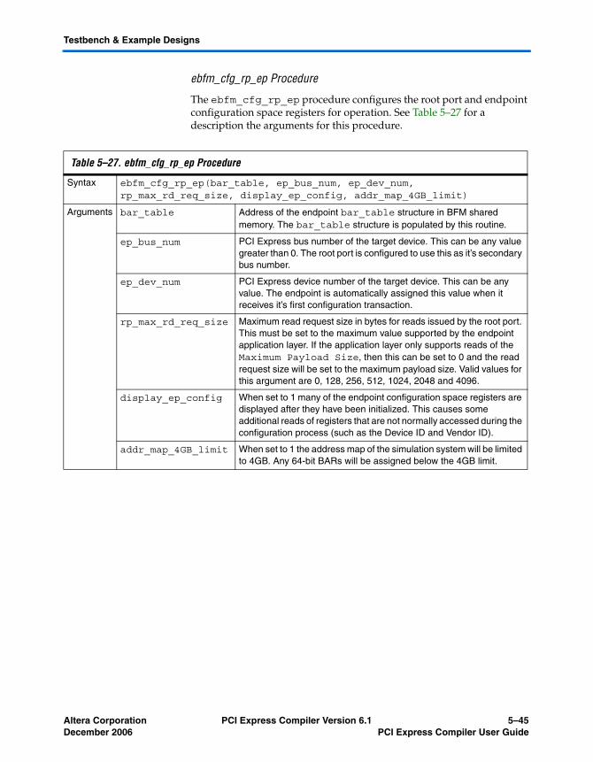
Testbench & Example Designs
ebfm_cfg_rp_ep Procedure
The ebfm_cfg_rp_ep procedure configures the root port and endpoint configuration space registers for operation. See Table 5–27 for a description the arguments for this procedure.
Table 5–27. ebfm_cfg_rp_ep Procedure
Syntax ebfm_cfg_rp_ep(bar_table, ep_bus_num, ep_dev_num, rp_max_rd_req_size, display_ep_config, addr_map_4GB_limit)
Arguments bar_table Address of the endpoint bar_table structure in BFM shared memory. The bar_table structure is populated by this routine.
ep_bus_num PCI Express bus number of the target device. This can be any value greater than 0. The root port is configured to use this as it’s secondary bus number.
ep_dev_num PCI Express device number of the target device. This can be any value. The endpoint is automatically assigned this value when it receives it’s first configuration transaction.
rp_max_rd_req_size Maximum read request size in bytes for reads issued by the root port. This must be set to the maximum value supported by the endpoint application layer. If the application layer only supports reads of the Maximum Payload Size, then this can be set to 0 and the read request size will be set to the maximum payload size. Valid values for this argument are 0, 128, 256, 512, 1024, 2048 and 4096.
display_ep_config When set to 1 many of the endpoint configuration space registers are displayed after they have been initialized. This causes some additional reads of registers that are not normally accessed during the configuration process (such as the Device ID and Vendor ID).
addr_map_4GB_limit When set to 1 the address map of the simulation system will be limited to 4GB. Any 64-bit BARs will be assigned below the 4GB limit.
Altera Corporation PCI Express Compiler Version 6.1 5–45December 2006 PCI Express Compiler User Guide
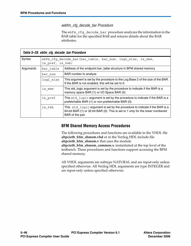
BFM Procedures and Functions
eebfm_cfg_decode_bar Procedure
The ebfm_cfg_decode_bar procedure analyzes the information in the BAR table for the specified BAR and returns details about the BAR attributes.
BFM Shared Memory Access Procedures
The following procedures and functions are available in the VHDL file altpcietb_bfm_shmem.vhd or in the Verilog HDL include file altpcietb_bfm_shmem.v that uses the module altpcietb_bfm_shmem_common.v, instantiated at the top level of the testbench. These procedures and functions support accessing the BFM shared memory.
All VHDL arguments are subtype NATURAL and are input-only unless specified otherwise. All Verilog HDL arguments are type INTEGER and are input-only unless specified otherwise.
Table 5–28. ebfm_cfg_decode_bar Procedure
Syntax ebfm_cfg_decode_bar(bar_table, bar_num, log2_size, is_mem, is_pref, is_64b)
Arguments bar_table Address of the endpoint bar_table structure in BFM shared memory
bar_num BAR number to analyze
log2_size This argument is set by the procedure to the Log Base 2 of the size of the BAR. If the BAR is not enabled, this will be set to 0
is_mem This std_logic argument is set by the procedure to indicate if the BAR is a memory space BAR (1) or I/O Space BAR (0)
is_pref This std_logic argument is set by the procedure to indicate if the BAR is a prefetchable BAR (1) or non-prefetchable BAR (0)
is_64b This std_logic argument is set by the procedure to indicate if the BAR is a 64-bit BAR (1) or 32-bit BAR (0). This is set to 1 only for the lower numbered BAR of the pair
5–46 PCI Express Compiler Version 6.1 Altera CorporationPCI Express Compiler User Guide December 2006

Testbench & Example Designs
Shared Memory Constants
The following constants are defined in the BFM shared memory package. They select a data pattern in the shmem_fill and shmem_chk_ok routines. These shared memory constants are all VHDL subtype NATURAL or Verilog HDL type INTEGER.
shmem_write
The shmem_write procedure writes data to the BFM shared memory.
Table 5–29. Constants: VHDL Subtype NATURAL or Verilog HDL Type INTEGER
Constant Description
SHMEM_FILL_ZEROS Specifies a data pattern of all zeros
SHMEM_FILL_BYTE_INC Specifies a data pattern of incrementing 8-bit bytes (0x00, 0x01, 0x02, etc.)
SHMEM_FILL_WORD_INC Specifies a data pattern of incrementing 16-bit words (0x0000, 0x0001, 0x0002, etc.)
SHMEM_FILL_DWORD_INC Specifies a data pattern of incrementing 32-bit double words (0x00000000, 0x00000001, 0x00000002, etc.)
SHMEM_FILL_QWORD_INC Specifies a data pattern of incrementing 64-bit quad words (0x0000000000000000, 0x0000000000000001, 0x0000000000000002, etc.)
SHMEM_FILL_ONE Specifies a data pattern of all ones
Table 5–30. shmem_write VHDL Procedure or Verilog HDL Task
Syntax shmem_write(addr, data, leng)
Arguments addr BFM shared memory starting address for writing data
data Data to write to BFM shared memory. In VHDL, this argument is an unconstrained std_logic_vector. This vector must be 8 times the leng long.In Verilog, this parameter is implemented as a 64-bit vector. leng is 1- 8 bytes.
In both languages, bits 7 downto 0 are written to the location specified by addr; bits 15 downto 8 are written to the addr+1 location, etc.
leng Length, in bytes, of data written
Altera Corporation PCI Express Compiler Version 6.1 5–47December 2006 PCI Express Compiler User Guide

BFM Procedures and Functions
shmem_read Function
The shmem_read function reads data to the BFM shared memory.
shmem_display VHDL Procedure or Verilog HDL Function
The shmem_display VHDL procedure or Verilog HDL function displays a block of data from the BFM shared memory.
Table 5–31. shmem_read Function
Syntax data:= shmem_read(addr, leng)
Arguments addr BFM shared memory starting address for reading data
leng Length, in bytes, of data read
Return data Data read from BFM shared memory.In VHDL, this is an unconstrained std_logic_vector, in which the vector is 8 times the leng long. In Verilog, this parameter is implemented as a 64-bit vector. leng is 1- 8 bytes. If the leng is less than 8 bytes, only the corresponding least significant bits of the returned data are valid.
In both languages, bits 7 downto 0 are read from the location specified by addr; bits 15 downto 8 are read from the addr+1 location, etc.
Table 5–32. shmem_display VHDL Procedure/ or Verilog Function
Syntax VHDL: shmem_display(addr, leng, word_size, flag_addr, msg_type)Verilog HDL: dummy_return:=shmem_display(addr, leng, word_size, flag_addr, msg_type);
Arguments addr BFM shared memory starting address for displaying data
leng Length, in bytes, of data to display
word_size Size of the words to display. Groups individual bytes into words. Valid values are 1, 2, 4, and 8
flag_addr Adds a <== flag to the end of the display line containing this address. Useful for marking specific data. Set to a value greater than 2**21 (size of BFM shared memory) to suppress the flag.
msg_type Specifies the message type to be displayed at the beginning of each line. See “BFM Log & Message Procedures” on page 5–50 for more information on message types. Should be on the constants defined in Table 5–35 on page 5–52.
5–48 PCI Express Compiler Version 6.1 Altera CorporationPCI Express Compiler User Guide December 2006

Testbench & Example Designs
shmem_fill Procedure
The shmem_fill procedure fills a block of BFM shared memory with a specified data pattern.
Table 5–33. shmem_fill Procedure
Syntax shmem_fill(addr, mode, leng, init)
Arguments addr BFM shared memory starting address for filling data
mode Data pattern used for filling the data. Should be one of the constants defined in section “Shared Memory Constants” on page 5–47.
leng Length, in bytes, of data to fill. If the length is not a multiple of the incrementing data pattern width, then the last data pattern is truncated to fit.
init Initial data value used for incrementing data pattern modes
In VHDL. this argument is type std_logic_vector(63 downto 0). In Verilog HDL, this argument is reg [63:0].
In both languages, the necessary least significant bits are used for the data patterns that are smaller than 64-bits.
Altera Corporation PCI Express Compiler Version 6.1 5–49December 2006 PCI Express Compiler User Guide

BFM Procedures and Functions
shmem_chk_ok Function
The shmem_chk_ok function checks a block of BFM shared memory against a specified data pattern.
BFM Log & Message Procedures
The following procedures and functions are available in the VHDL package file altpcietb_bfm_log.vhd or in the Verilog HDL include file altpcietb_bfm_log.v that uses the altpcietb_bfm_log_common.v module, instantiated at the top level of the testbench.
These procedures provide support for displaying messages in a common format, suppressing informational messages, and stopping simulation on specific message types.
Table 5–34. shmem_chk_ok Function
Syntax result:= shmem_chk_ok(addr, mode, leng, init, display_error)
Arguments addr BFM shared memory starting address for checking data.
mode Data pattern used for checking the data. Should be one of the constants defined in section “Shared Memory Constants” on page 5–47.
leng Length, in bytes, of data to check.
init In VHDL. this argument is type std_logic_vector(63 downto 0). In Verilog HDL, this argument is reg [63:0].
In both languages, the necessary least significant bits are used for the data patterns that are smaller than 64-bits.
display_error When set to 1, this argument displays the mis-comparing data on the simulator standard output.
Return Result Result is VHDL type Boolean.TRUE—Data pattern compared successfullyFALSE—Data pattern did not compare successfully
Result in Verilog HDL is 1-bit.1’b1 — Data patterns compared successfully1’b0 — Data patterns did not compare successfully
5–50 PCI Express Compiler Version 6.1 Altera CorporationPCI Express Compiler User Guide December 2006

Testbench & Example Designs
Log Constants
The following constants are defined in the BFM Log package. They define the type of message and their values determine whether a message is displayed or simulation is stopped after a specific message. Each displayed message has a specific prefix, based on the message type in Table 5–35.
You can suppress the display of certain message types. For the default value determining whether a message type is displayed, see Table 5–35. To change the default message display, modify the display default value with a procedure call to ebfm_log_set_suppressed_msg_mask.
Certain message types also stop simulation after the message is displayed. Table 5–35 shows the default value determining whether a message type stops simulation. You can specify whether simulation stops for particular messages with the procedure ebfm_log_set_stop_on_msg_mask.
All of these log message constants are VHDL subtype NATURAL or type INTEGER for Verilog HDL.
ebfm_display VHDL Procedure or Verilog HDL Function
The ebfm_display procedure or function displays a message of the specified type to the simulation standard output and also the log file if ebfm_log_open() is called.
A message can be suppressed and/or simulation stopped based on the default settings of the message type and the value of the bit mask for each of the procedures below when each is called. You can call one or both of these procedures based on what messages you want displayed and whether or not you want simulation to stop for specific messages.
■ When ebfm_log_set_suppressed_msg_mask() is called, the display of the message might be suppressed based on the value of the bit mask.
■ When ebfm_log_set_stop_on_msg_mask() is called, the simulation can be stopped after the message is displayed, based on the value of the bit mask.
Altera Corporation PCI Express Compiler Version 6.1 5–51December 2006 PCI Express Compiler User Guide

BFM Procedures and Functions
Table 5–35. Log Messages Using VHDL Constants - Subtype NATURAL (Part 1 of 2)
Constant (Message Type) DescriptionMask
Bit Number
Display by
Default
Simulation Stops by Default
Message Prefix
EBFM_MSG_DEBUG Specifies Debug Messages.
0 N N DEBUG:
EBFM_MSG_INFO Specifies informational messages, such as configuration register values, starting and ending of tests, etc.
1 Y N INFO:
EBFM_MSG_WARNING Specifies warning messages, such as tests being skipped due to the specific configuration, etc.
2 Y N WARNING:
EBFM_MSG_ERROR_INFO Specifies additional information for an error. Use this message to display preliminary information before an error message that stops simulation.
3 Y N ERROR:
EBFM_MSG_ERROR_CONTINUE Specifies a recoverable error that allows simulation to continue. The error can be something like a data mis-compare.
4 Y N ERROR:
EBFM_MSG_ERROR_FATAL Specifies an error that stops simulation because the error left the testbench in a state where further simulation is not possible.
N/A YCannot suppress
YCannot suppress
FATAL:
5–52 PCI Express Compiler Version 6.1 Altera CorporationPCI Express Compiler User Guide December 2006

Testbench & Example Designs
EBFM_MSG_ERROR_FATAL_TB_ERR Used for BFM test driver or root port BFM fatal errors. Specifies an error that stops simulation because the error left the testbench in a state where further simulation is not possible. Use this error message for errors that occur due to a problem in the BFM test driver module or the root port BFM, and is not caused by the endpoint application layer being tested.
N/A YCannot suppress
YCannot suppress
FATAL:
Table 5–35. Log Messages Using VHDL Constants - Subtype NATURAL (Part 2 of 2)
Constant (Message Type) DescriptionMask
Bit Number
Display by
Default
Simulation Stops by Default
Message Prefix
Table 5–36. ebfm_display Procedure
Syntax VHDL: ebfm_display(msg_type, message)Verilog HDL: dummy_return:=ebfm_display(msg_type, message);
Argument msg_type Message type for the message. Should be one of the constants defined in Table 5–35 on page 5–52.
message In VHDL, this argument is VHDL type string and contains the message text to be displayed.
In Verilog HDL, the message string is limited to a maximum of 100 characters. Also, because Verilog HDL does not allow variable length string This routine strips off leading characters of 8’h00 before displaying the message.
Return always 0 This applies only to the Verilog HDL routine.
Altera Corporation PCI Express Compiler Version 6.1 5–53December 2006 PCI Express Compiler User Guide

BFM Procedures and Functions
ebfm_log_stop_sim VHDL Procedure or Verilog HDL Function
The ebfm_log_stop_sim procedure stops the simulation.
ebfm_log_set_suppressed_msg_mask Procedure
The ebfm_log_set_suppressed_msg_mask procedure controls which message types are suppressed. This alters the Displayed by Default settings described in Table 5–35 on page 5–52.
Table 5–37. ebfm_log_stop_sim Procedure
Syntax VHDL: ebfm_log_stop_sim(success)Verilog VHDL: return:=ebfm_log_stop_sim(success);
Argument success When set to a 1, this process stops the simulation with a message indicating successful completion. The message is prefixed with SUCCESS:.
Otherwise, this process stops the simulation with a message indicating unsuccessful completion. The message is prefixed with FAILURE:.
Return Always 0 This value applies only to the Verilog HDL function.
Table 5–38. ebfm_log_set_suppressed_msg_mask Procedure
Syntax bfm_log_set_suppressed_msg_mask (msg_mask)
Argument msg_mask In VHDL, this argument is a subtype of std_logic_vector, EBFM_MSG_MASK. This vector has a range from EBFM_MSG_ERROR_CONTINUE downto EBFM_MSG_DEBUG.In Verilog HDL, this argument is reg [EBFM_MSG_ERROR_CONTINUE: EBFM_MSG_DEBUG].In both languages, a 1 in a specific bit position of the msg_mask causes messages of the type corresponding to the bit position to be suppressed.
5–54 PCI Express Compiler Version 6.1 Altera CorporationPCI Express Compiler User Guide December 2006

Testbench & Example Designs
ebfm_log_set_stop_on_msg_mask Procedure
The ebfm_log_set_stop_on_msg_mask procedure controls which message types stop simulation. This alters the Stop Sim by Default settings described in Table 5–35 on page 5–52.
ebfm_log_open Procedure
The ebfm_log_open procedure opens a log file of the specified name. All displayed messages are called by ebfm_display and are written to this log file as simulator standard output.
ebfm_log_close Procedure
The ebfm_log_close procedure closes the log file opened by a previous call to ebfm_log_open.
Table 5–39. ebfm_log_set_stop_on_msg_mask Procedure
Syntax ebfm_log_set_stop_on_msg_mask (msg_mask)
Argument msg_mask In VHDL, this argument is a subtype of std_logic_vector, EBFM_MSG_MASK. This vector has a range from EBFM_MSG_ERROR_CONTINUE downto EBFM_MSG_DEBUG.In Verilog HDL, this argument is reg [EBFM_MSG_ERROR_CONTINUE:EBFM_MSG_DEBUG].In both languages, a 1 in a specific bit position of the msg_mask causes messages of the type corresponding to the bit position to stop the simulation after the message is displayed.
Table 5–40. ebfm_log_open Procedure
Syntax ebfm_log_open (fn)
Argument fn This argument is type string. File name of log file to be opened
Table 5–41. ebfm_log_close Procedure
Syntax ebfm_log_close
Argument NONE
Altera Corporation PCI Express Compiler Version 6.1 5–55December 2006 PCI Express Compiler User Guide

BFM Procedures and Functions
himage (std_logic_vector) Function
The himage function is a utility routine that returns a hexadecimal string representation of the std_logic_vector argument. The string is the length of the std_logic_vector divided by four (rounded up). You can control the length of the string by padding or truncating the argument as needed.
himage (integer) Function
The himage function is a utility routine that returns a hexadecimal string representation of the integer argument. The string is the length specified by the hlen argument.
Verilog HDL Formatting Functions
This section outlines formatting functions that are only used by Verilog HDL. All these functions take one argument of a specified length and return a vector of a specified length.
Table 5–42. himage (std_logic_vector) Function
Syntax string:= himage(vec)
Argument vec This argument is a std_logic_vector that is converted to a hexadecimal string.
Return String Hexadecimal formatted string representation of the argument
Table 5–43. himage (integer) Function
Syntax string:= himage(num, hlen)
Arguments num Argument of type integer that is converted to a hexadecimal string
hlen Length of the returned string. The string is truncated or padded with 0’s on the right as needed.
Return string Hexadecimal formatted string representation of the argument
5–56 PCI Express Compiler Version 6.1 Altera CorporationPCI Express Compiler User Guide December 2006

Testbench & Example Designs
himage1
This function creates a 1-digit hexadecimal string representation of the input argument that can be concatenated into a larger message string and passed to ebfm_display.
himage2
This function creates a 2-digit hexadecimal string representation of the input argument that can be concatenated into a larger message string and passed to ebfm_display.
himage4
This function creates a 4-digit hexadecimal string representation of the input argument can be concatenated into a larger message string and passed to ebfm_display.
Table 5–44. himage1
syntax string:= himage(vec)
Argument vec Input data type reg with a range of 3:0.
Return range string Returns a 1-digit hexadecimal representation of the input argument. Return data is type reg with a range of 8:1
Table 5–45. himage2
syntax string:= himage(vec)
Argument range vec Input data type reg with a range of 7:0.
Return range string Returns a 2-digit hexadecimal presentation of the input argument, padded with leading 0’s, if they are needed. Return data is type reg with a range of 16:1
Table 5–46. himage4
syntax string:= himage(vec)
Argument range vec Input data type reg with a range of 15:0.
Return range string Returns a 4-digit hexadecimal representation of the input argument, padded with leading 0’s, if they are needed. Return data is type reg with a range of 32:1
Altera Corporation PCI Express Compiler Version 6.1 5–57December 2006 PCI Express Compiler User Guide

BFM Procedures and Functions
himage8
This function creates an 8-digit hexadecimal string representation of the input argument that can be concatenated into a larger message string and passed to ebfm_display.
himage16
This function creates a 16-digit hexadecimal string representation of the input argument that can be concatenated into a larger message string and passed to ebfm_display.
dimage1
This function creates a 1-digit hexadecimal string representation of the input argument that can be concatenated into a larger message string and passed to ebfm_display.
Table 5–47. himage8
syntax string:= himage(vec)
Argument range vec Input data type reg with a range of 31:0.
Return range string Returns an 8-digit hexadecimal representation of the input argument, padded with leading s 0’s, if they are needed. Return data is type reg with a range of 64:1
Table 5–48. himage16
syntax string:= himage(vec)
Argument range vec Input data type reg with a range of 63:0.
Return range string Returns a 16-digit hexadecimal representation of the input argument, padded with leading 0’s, if they are needed. Return data is type reg with a range of 128:1
Table 5–49. dimage1
syntax string:= dimage(vec)
Argument range vec Input data type reg with a range of 31:0.
Return range string Returns a 1-digit decimal representation of the input argument that is padded with leading 0’s if necessary. Return data is type reg with a range of 8:1.
Returns the letter U if the value cannot be represented.
5–58 PCI Express Compiler Version 6.1 Altera CorporationPCI Express Compiler User Guide December 2006

Testbench & Example Designs
dimage2
This function creates a 2-digit hexadecimal string representation of the input argument that can be concatenated into a larger message string and passed to ebfm_display.
dimage3
This function creates a 3-digit hexadecimal string representation of the input argument that can be concatenated into a larger message string and passed to ebfm_display.
dimage4
This function creates a 4-digit hexadecimal string representation of the input argument that can be concatenated into a larger message string and passed to ebfm_display.
Table 5–50. dimage2
syntax string:= dimage(vec)
Argument range vec Input data type reg with a range of 31:0.
Return range string Returns a 2-digit decimal representation of the input argument that is padded with leading 0’s if necessary. Return data is type reg with a range of 16:1.
Returns the letter U if the value cannot be represented.
Table 5–51. dimage3
syntax string:= dimage(vec)
Argument range vec Input data type reg with a range of 31:0.
Return range string Returns a 3-digit decimal representation of the input argument that is padded with leading 0’s if necessary. Return data is type reg with a range of 24:1.
Returns the letter U if the value cannot be represented.
Table 5–52. dimage4
syntax string:= dimage(vec)
Argument range vec Input data type reg with a range of 31:0.
Return range string Returns a 4-digit decimal representation of the input argument that is padded with leading 0’s if necessary. Return data is type reg with a range of 32:1.
Returns the letter U if the value cannot be represented.
Altera Corporation PCI Express Compiler Version 6.1 5–59December 2006 PCI Express Compiler User Guide

BFM Procedures and Functions
dimage5
This function creates a 5-digit hexadecimal string representation of the input argument that can be concatenated into a larger message string and passed to ebfm_display.
dimage6
This function creates a 6-digit hexadecimal string representation of the input argument that can be concatenated into a larger message string and passed to ebfm_display.
dimage7
This function creates a 7-digit hexadecimal string representation of the input argument that can be concatenated into a larger message string and passed to ebfm_display.
Table 5–53. dimage5
syntax string:= dimage(vec)
Argument range vec Input data type reg with a range of 31:0.
Return range string Returns a 5-digit decimal representation of the input argument that is padded with leading 0’s if necessary. Return data is type reg with a range of 40:1.
Returns the letter U if the value cannot be represented.
Table 5–54. dimage6
syntax string:= dimage(vec)
Argument range vec Input data type reg with a range of 31:0.
Return range string Returns a 6-digit decimal representation of the input argument that is padded with leading 0’s if necessary. Return data is type reg with a range of 48:1.
Returns the letter U if the value cannot be represented.
Table 5–55. dimage7
syntax string:= dimage(vec)
Argument range vec Input data type reg with a range of 31:0.
Return range string Returns a 7-digit decimal representation of the input argument that is padded with leading 0’s if necessary. Return data is type reg with a range of 56:1.
Returns the letter U if the value cannot be represented.
5–60 PCI Express Compiler Version 6.1 Altera CorporationPCI Express Compiler User Guide December 2006

Testbench & Example Designs
Procedures and Functions Specific to the chaining DMA Design
This section describes procedures that are specific to the chaining DMA example design.
chained_dma_test Procedure
The chained_dma_test procedure is the top level procedure that runs the chaining DMA read and the chaining DMA write
dma_rd_test Procedure
The dma_rd_test procedure is used for DMA read, from the Endpoint memory to the BFM shared memory.
Table 5–56. chained_dma_test Procedure
Syntax chained_dma_test (bar_table, bar_num, direction, use_msi, use_eplast)
Arguments bar_table Address of the endpoint bar_table structure in BFM shared memory
bar_num BAR number to analyze
direction When 0 read, When 1 write, When 2 Read then Write When 3 Write then Read
Use_msi When set, the Root Port uses native PCI express MSI to detect the DMA completion
Use_eplast When set, the Root Port uses BFM shared memory polling to detect the DMA completion.
Table 5–57. dma_rd_test Procedure
Syntax dma_rd_test (bar_table, bar_num, use_msi, use_eplast)
Arguments bar_table Address of the endpoint bar_table structure in BFM shared memory
bar_num BAR number to analyze
Use_msi When set, the Root Port uses native PCI express MSI to detect the DMA completion
Use_eplast When set, the Root Port uses BFM shared memory polling to detect the DMA completion.
Altera Corporation PCI Express Compiler Version 6.1 5–61December 2006 PCI Express Compiler User Guide

BFM Procedures and Functions
dma_wr_test Procedure
The dma_wr_test procedure is used for DMA write, from the BFM shared memory to the Endpoint memory.
dma_set_rd_desc_data Procedure
The dma_set_rd_desc_data procedure is used for to configure the BFM shared memory for the DMA read.
dma_set_wr_desc_data Procedure
The dma_set_wr_desc_data procedure is used for to configure the BFM shared memory for the DMA write.
dma_set_header Procedure
The dma_set_header procedure is used for to configure the DMA descriptor table for DMA read or DMA write.
Table 5–58. dma_wr_test Procedure
Syntax dma_wr_test (bar_table, bar_num, use_msi, use_eplast)
Arguments bar_table Address of the endpoint bar_table structure in BFM shared memory
bar_num BAR number to analyze
Use_msi When set, the Root Port uses native PCI express MSI to detect the DMA completion
Use_eplast When set, the Root Port uses BFM shared memory polling to detect the DMA completion.
Table 5–59. dma_set_rd_desc_data Procedure
Syntax dma_set_rd_desc_data (bar_table, bar_num)
Arguments bar_table Address of the endpoint bar_table structure in BFM shared memory
bar_num BAR number to analyze
Table 5–60. dma_set_wr_desc_data Procedure
Syntax dma_set_wr_desc_data (bar_table, bar_num)
Arguments bar_table Address of the endpoint bar_table structure in BFM shared memory
bar_num BAR number to analyze
5–62 PCI Express Compiler Version 6.1 Altera CorporationPCI Express Compiler User Guide December 2006

Testbench & Example Designs
Table 5–61. dma_set_wr_desc_data Procedure
Syntax dma_set_wr_desc_data (bar_table, bar_num)
Arguments bar_table Address of the endpoint bar_table structure in BFM shared memory
bar_num BAR number to analyze
Descriptor_size Number of descriptor
direction When 0 read, When 1 write,
Use_msi When set, the Root Port uses native PCI express MSI to detect the DMA completion
Use_eplast When set, the Root Port uses BFM shared memory polling to detect the DMA completion.
Bdt_msb BFM shared memory upper address value
Bdt_lsb BFM shared memory lower address value
Msi number When use_msi is set, this specifies the number of msi which is set by the procedure dma_set_msi
Msi_traffic_class When use_msi is set, this specifies the MSI traffic class which is set by the procedure dma_set_msi
msi_expected_dmawr When use_msi is set, this specifies expected MSI data value which is set by the procedure dma_set_msi
Multi_message_enable When use_msi is set, this specifies the MSI traffic class which is set by the procedure dma_set_msi
Altera Corporation PCI Express Compiler Version 6.1 5–63December 2006 PCI Express Compiler User Guide

BFM Procedures and Functions
rc_poll Procedure
The rc_poll procedure is used to polled a given DWORD in a given BFM shared memory location
.
msi_poll Procedure
The msi_poll procedure tracks MSI completion from the endpoint.
Table 5–62. rc_poll Procedure
Syntax rc_poll (rc_addr, rc_data)
Arguments rc_addr Address of the BFM shared memory which is being polled
rc_data Expected data value of the which is being polled
Table 5–63. msi_poll Procedure
Syntax dma_set_wr_desc_data (bar_table, bar_num)
Arguments Dma_read When set, poll MSI from the DMA read module
Dma_write When set, poll MSI from the DMA write module
Msi number When use_msi is set, this specifies the number of msi which is set by the procedure dma_set_msi
Msi_traffic_class When use_msi is set, this specifies the MSI traffic class which is set by the procedure dma_set_msi
msi_expected_dmawr When use_msi is set, this specifies expected MSI data value which is set by the procedure dma_set_msi
Multi_message_enable When use_msi is set, this specifies the MSI traffic class which is set by the procedure dma_set_msi
5–64 PCI Express Compiler Version 6.1 Altera CorporationPCI Express Compiler User Guide December 2006

Testbench & Example Designs
dma_set_msi Procedure
The dma_set_msi procedure sets PCI Express native MSI for the DMA read or the DMA write..
Table 5–64. dma_set_msi Procedure
Syntax et_msi (bar_table, bar_num)
Arguments bar_table Address of the endpoint bar_table structure in BFM shared memory
bar_num BAR number to analyze
Bus_num Set configuration bus number
dev_num Set configuration device number
Fun_num Set configuration function number
Direction When 0 read When 1 write
Msi number Returns the number of msi
Msi_traffic_class Returns the MSI traffic class value
msi_expected_dmawr Returns the expected MSI data value
Multi_message_enable Returns the MSI multi message enable status
Altera Corporation PCI Express Compiler Version 6.1 5–65December 2006 PCI Express Compiler User Guide

BFM Procedures and Functions
5–66 PCI Express Compiler Version 6.1 Altera CorporationPCI Express Compiler User Guide December 2006

Altera Corporation PCI ExDecember 2006
Appendix A.Configuration Signals
Configuration Signals for x1 and x4 MegaCore Functions
Table A–1 shows all of the MegaCore function’s available configuration signals for x1 and x4 MegaCore functions. These signals are set internal to the variation file created by the Quartus II software. They should not be modified except by MegaWizard interface. They are provided here for reference.
Table A–1. Configuration Signals for x1 and x4 MegaCore Functions (Part 1 of 6)
Signal Value or Wizard Page/Label Description
k_gbl[0] Fixed to 0 PCI Express specification compliance setting. When the value is set to 1, the MegaCore function is set to be compliant with the PCI Express 1.1 specification.When the value is set to 0, the MegaCore function is set to be compliant with PCI Express 1.0a specification.
k_gbl[9:1] Fixed to 0 Reserved.
k_gbl[10] Capabilities: Link Common Clock
Clock configuration, 0 = system reference clock not used, 1 = system reference clock used for PHY.
k_gbl[11] Fixed to 0 Reserved.
k_gbl[15:12] System: Interface Type Port type: 0 = native EP, 1 = legacy EP.
k_gbl[25:16] Fixed to 0 Reserved.
k_gbl[26] Fixed to 1 Implement reordering on receive path.
k_gbl[31:27] Fixed to 0 Reserved.
k_conf[15:0] Capabilities: Vendor ID Vendor ID register.
k_conf[31:16] Capabilities: Device ID Device ID register.
k_conf[39:32] Capabilities: Revision ID Revision ID register.
k_conf[63:40] Capabilities: Class Code Class code register.
k_conf[79:64] Capabilities: Subsystem Vendor ID
Subsystem vendor ID register.
k_conf[95:80] Capabilities: Subsystem Device ID
Subsystem device ID register.
k_conf[98:96] Fixed to 0b010 Power management capabilities register version field (set to 010).
press Compiler Version 6.1 A–1

Configuration Signals for x1 and x4 MegaCore Functions
k_conf[99] Fixed to 0 Power management capabilities register PME clock field.
k_conf[100] Fixed to 0 Reserved.
k_conf[101] Fixed to 0 Power management capabilities register device-specific initialization (DSI) field.
k_conf[104:102] Fixed to 0 Power management capabilities register maximum auxiliary current required while in d3cold to support PME.
k_conf[105] Fixed to 0 Power management capabilities register D1 support bit.
k_conf[106] Fixed to 0 Power management capabilities register D2 support bit.
k_conf[107] Fixed to 0 Power management capabilities register PME message can be sent in D0 state bit.
k_conf[108] Fixed to 0 Power management capabilities register PME message can be sent in D1 state bit.
k_conf[109] Fixed to 0 Power management capabilities register PME message can be sent in D2 state bit.
k_conf[110] Fixed to 0 Power management capabilities register PME message can be sent in D3 hot state bit.
k_conf[111] Fixed to 0 Power management capabilities register PME message can be sent in D3 cold state bit.
k_conf[112] Capabilities: Implement AER
Advanced error reporting capability supported.
k_conf[115:113] Buffer Setup: Low Priority Virtual Channels
Port VC capability register 1 low priority VC field.
k_conf[119:116] Fixed to 0b0001 Port VC capability register 2 VC arbitration capability field.
k_conf[127:120] Fixed to 0 Reserved.
k_conf[130:128] Fixed to 0 Reserved.
k_conf[132:131] Fixed to 0 Reserved.
k_conf[133] Calculated Device capabilities register: extended tag field supported. Set to 1 when number of tags > 32.
k_conf[136:134] Power Management: Endpoint L0s Acceptable Latency
Device capabilities register: endpoint L0s acceptable latency. 0 = < 64 ns, 1 = 64 - 128 ns, 2 = 128 - 256 ns, 3 = 256 - 512 ns, 4 = 512 ns - 1 μs, 5 = 1 - 2 μs, 6 = 2 -4 μs, 7 => 4 μs.
Table A–1. Configuration Signals for x1 and x4 MegaCore Functions (Part 2 of 6)
Signal Value or Wizard Page/Label Description
A–2 PCI Express Compiler Version 6.1 Altera CorporationPCI Express Compiler User Guide December 2006

k_conf[139:137] Power Management: Endpoint L1 Acceptable Latency
Device capabilities register: endpoint L1 acceptable latency. 0 =< 1 μs, 1 = 1 - 2 μs, 2 = 2 - 4 μs, 3 = 4 - 8 μs, 4 = 8 - 16 μs, 5 = 16 - 32 μs, 6 = 32 - 64 μs, 7 => 64 μs.
k_conf[143:140] Fixed to 0 Reserved.
k_conf[145:144] Fixed to 0 Reserved.
k_conf[151:146] Calculated from the number of lanes
Link capabilities register: maximum link width. 1 = x1, 4 = x4, others = reserved.
k_conf[153:152] Power Management: Enable L1 ASPM
Link capabilities register: active state power management support. 01 = L0s, 11 = L1 and L0s.
k_conf[156:154] Power Management: L1 Exit Latency Common Clock
Link capabilities register: L1 exit latency - separate clock. 0 =< 1 μs, 1 = 1 - 2 μs, 2 = 2 - 4 μs, 3 = 4 - 8 μs, 4 = 8 - 16 μs, 5 = 16 - 32 μs, 6 = 32 - 64 μs, 7 =>64 μs.
k_conf[159:157] Power Management: L1 Exit Latency Separate Clock
Link capabilities register: L1 exit latency - common clock. 0 =< 1 μs, 1 = 1 - 2 μs, 2 = 2 - 4 μs, 3 = 4 - 8 μs, 4 = 8 - 16 μs, 5 = 16 - 32 μs, 6 = 32 - 64 μs, 7 => 64 μs.
k_conf[166:160] Fixed to 0 Reserved.
k_conf[169:167] Capabilities: Tags Supported
Number of tags supported for non-posted requests transmitted.
k_conf[191:170] Fixed to 0 Reserved.
k_conf[199:192] Power Management: N_FTS Separate
Number of fast training sequences needed in separate clock mode (N_FTS).
k_conf[207:200] Power Management: N_FTS Common
Number of fast training sequences needed in common clock mode (N_FTS).
k_conf[215:208] Capabilities: Link Port Number
Link capabilities register: port number.
k_conf[216] Capabilities: Implement ECRC Check
Advanced error capabilities register: ECRC check enable.
k_conf[217] Capabilities: Implement ECRC Generation
Advanced error capabilities register: ECRC generation enable.
k_conf[218] Fixed to 0 Reserved.
k_conf[221:219] Capabilities: MSI Messages Requested
MSI capability message control register: multiple message capable request field. 0 = 1 message, 1 = 2 messages, 2 = 4 messages, 3 = 8 messages, 4 = 16 messages, 5 = 32 messages.
k_conf[222] Capabilities: MSI Message 64 bit Capable
MSI capability message control register: 64-bit capable. 0 = 32b, 1 = 64b or 32b.
k_conf[223] Capabilities: MSI Per Vector Masking
Per-bit vector masking (RO field).
Table A–1. Configuration Signals for x1 and x4 MegaCore Functions (Part 3 of 6)
Signal Value or Wizard Page/Label Description
Altera Corporation PCI Express Compiler Version 6.1 A–3December 2006 PCI Express Compiler User Guide

Configuration Signals for x1 and x4 MegaCore Functions
k_bar[31:0] System: BAR Table (BAR0)
BAR0 size mask and read only fields (I/O space, memory space, prefetchable). bit 31 - 4 = size mask, bit 3 = prefetchable, bit 2 = 64 bit, bit 1 = 0, bit 0 = I/O.
k_bar[63:32] System: BAR Table (BAR1)
BAR1 size mask and read only fields (I/O space, memory space, prefetchable). bit 31 - 4 = size mask, bit 3 = prefetchable, bit 2 = 64 bit, bit 1 = 0, bit 0 = I/O (or bit 31 - 0 = size mask if previous 64 bit).
k_bar[95:64] System: BAR Table (BAR2)
BAR2 size mask and read only fields (I/O space, memory space, prefetchable). bit 31 - 4 = size mask, bit 3 = prefetchable, bit 2 = 64 bit, bit 1 = 0, bit 0 = I/O.
k_bar[127:96] System: BAR Table (BAR3)
BAR3 size mask and read only fields (I/O space, memory space, prefetchable). bit 31 - 4 = size mask, bit 3 = Prefetchable, bit 2 = 64 bit, bit 1 = 0, bit 0 = I/O (or bit 31 - 0 = size mask if previous 64 bit).
k_bar[159:128] System: BAR Table (BAR4)
BAR4 size mask and read only fields (I/O space, memory space, prefetchable). bit 31 - 4 = size mask, bit 3 = prefetchable, bit 2 = 64 bit, bit 1 = 0, bit 0 = I/O.
k_bar[191:160] System: BAR Table (BAR5)
BAR5 size mask and read only fields (I/O space, memory space, prefetchable). bit 31 - 4 = size mask, bit 3 = prefetchable, bit 2 = 64 bit, bit1 = 0, bit 0 = I/O (or bit 31 - 0 = size mask if previous 64 bit).
k_bar[223:192] System: BAR Table (Exp ROM)
Expansion ROM BAR size mask. bit 31 - 11 = size mask, bit 10 - 1 = 0, bit 0 = enable.
k_cnt[95:0] Fixed to 0 Reserved.
k_cnt[106:96] Fixed to 17 Flow control initialization timer (number in μs). Number in cycles.
k_cnt[111:107] Power Management: Idle Threshold for L0s Entry
Idle threshold for L0s entry (in 256 ns steps).
k_cnt[116:112] Fixed to 30 Update flow control credit timer (number in μs).
k_cnt[119:117] Fixed to 0 Reserved.
k_cnt[127:120] Fixed to 200 Flow control Time-Out check (number in μs).
k_vc0[7:0] Calculated: VC Table Posted Header Credit
Receive flow control credit for VC0 posted headers.
k_vc0[19:8] Calculated: VC Table Posted Data Credit
Receive flow control credit for VC0 posted data.
k_vc0[27:20] Calculated: VC Table Non-Posted Header Credit
Receive flow control credit for VC0 non-posted headers.
Table A–1. Configuration Signals for x1 and x4 MegaCore Functions (Part 4 of 6)
Signal Value or Wizard Page/Label Description
A–4 PCI Express Compiler Version 6.1 Altera CorporationPCI Express Compiler User Guide December 2006

k_vc0[35:28] Fixed to 0 Receive flow control credit for VC0 non-posted data. The Rx buffer always has space for the maximum 1 DWORD of data that can be sent for non-posted writes (configuration or I/O writes).
k_vc0[43:36] Fixed to 0 Receive flow control credit for VC0 completion headers. Infinite completion credits must be advertised by endpoints.
k_vc0[55:44] Fixed to 0 Receive flow control credit for VC0 completion data. Infinite completion credits must be advertised by endpoints.
k_vc1[7:0] Calculated: VC Table Posted Header Credit
Receive flow control credit for VC1 posted headers.
k_vc1[19:8] Calculated: VC Table Posted Data Credit
Receive flow control credit for VC1 posted data.
k_vc1[27:20] Calculated: VC Table Non-Posted Header Credit
Receive flow control credit for VC1 non-posted headers.
k_vc1[35:28] Fixed to 0 Receive flow control credit for VC1 non-posted data. Non-posted writes (configuration and I/O writes) only use VC0.
k_vc1[43:36] Fixed to 0 Receive flow control credit for VC1 completion headers. Infinite completion credits must be advertised by endpoints.
k_vc1[55:44] Fix to 0 Receive flow control credit for VC1 completion data. Infinite completion credits must be advertised by endpoints.
k_vc2[7:0] Calculated: VC Table Posted Header Credit
Receive flow control credit for VC2 posted headers.
k_vc2[19:8] Calculated: VC Table Posted Data Credit
Receive flow control credit for VC2 posted data.
k_vc2[27:20] Calculated: VC Table Non-Posted Header Credit
Receive flow control credit for VC2 non-posted headers.
k_vc2[35:28] Fixed to 0 Receive flow control credit for VC2 non-posted data. Non-posted writes (configuration and I/O writes) only use VC0.
k_vc2[43:36] Fixed to 0 Receive flow control credit for VC2 completion headers. Infinite completion credits must be advertised by endpoints.
k_vc2[55:44] Fixed to 0 Receive flow control credit for VC2 completion data. Infinite completion credits must be advertised by endpoints.
Table A–1. Configuration Signals for x1 and x4 MegaCore Functions (Part 5 of 6)
Signal Value or Wizard Page/Label Description
Altera Corporation PCI Express Compiler Version 6.1 A–5December 2006 PCI Express Compiler User Guide
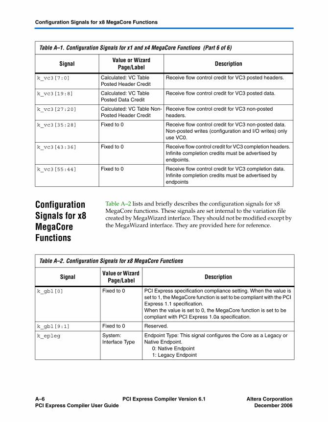
Configuration Signals for x8 MegaCore Functions
Configuration Signals for x8 MegaCore Functions
Table A–2 lists and briefly describes the configuration signals for x8 MegaCore functions. These signals are set internal to the variation file created by MegaWizard interface. They should not be modified except by the MegaWizard interface. They are provided here for reference.
k_vc3[7:0] Calculated: VC Table Posted Header Credit
Receive flow control credit for VC3 posted headers.
k_vc3[19:8] Calculated: VC Table Posted Data Credit
Receive flow control credit for VC3 posted data.
k_vc3[27:20] Calculated: VC Table Non-Posted Header Credit
Receive flow control credit for VC3 non-posted headers.
k_vc3[35:28] Fixed to 0 Receive flow control credit for VC3 non-posted data. Non-posted writes (configuration and I/O writes) only use VC0.
k_vc3[43:36] Fixed to 0 Receive flow control credit for VC3 completion headers. Infinite completion credits must be advertised by endpoints.
k_vc3[55:44] Fixed to 0 Receive flow control credit for VC3 completion data. Infinite completion credits must be advertised by endpoints
Table A–1. Configuration Signals for x1 and x4 MegaCore Functions (Part 6 of 6)
Signal Value or Wizard Page/Label Description
Table A–2. Configuration Signals for x8 MegaCore Functions
Signal Value or Wizard Page/Label Description
k_gbl[0] Fixed to 0 PCI Express specification compliance setting. When the value is set to 1, the MegaCore function is set to be compliant with the PCI Express 1.1 specification.When the value is set to 0, the MegaCore function is set to be compliant with PCI Express 1.0a specification.
k_gbl[9:1] Fixed to 0 Reserved.
k_epleg System: Interface Type
Endpoint Type: This signal configures the Core as a Legacy or Native Endpoint.
0: Native Endpoint1: Legacy Endpoint
A–6 PCI Express Compiler Version 6.1 Altera CorporationPCI Express Compiler User Guide December 2006

k_rxro Fixed to 1 Receive Reordering: This signal implements reordering capabilities on the Receive Path.
0: no Receive reordering1: Receive reordering
k_conf[15:0] Capabilities: Vendor ID
Vendor ID register.
k_conf[31:16] Capabilities: Device ID
Device ID register.
k_conf[39:32] Capabilities: Revision ID
Revision ID register.
k_conf[63:40] Capabilities: Class Code
Class code register.
k_conf[79:64] Capabilities: Subsystem Vendor ID
Subsystem vendor ID register.
k_conf[95:80] Capabilities: Subsystem Device ID
Subsystem device ID register.
k_conf[98:96] Fixed to 0b010 Power management capabilities register version field (set to 010).
k_conf[99] Fixed to 0 Power management capabilities register PME clock field.
k_conf[100] Fixed to 0 Reserved.
k_conf[101] Fixed to 0 Power management capabilities register device-specific initialization (DSI) field.
k_conf[104:102] Fixed to 0 Power management capabilities register maximum auxiliary current required while in d3cold to support PME.
k_conf[105] Fixed to 0 Power management capabilities register D1 support bit.
k_conf[106] Fixed to 0 Power management capabilities register D2 support bit.
k_conf[107] Fixed to 0 Power management capabilities register PME message can be sent in D0 state bit.
k_conf[108] Fixed to 0 Power management capabilities register PME message can be sent in D1 state bit.
k_conf[109] Fixed to 0 Power management capabilities register PME message can be sent in D2 state bit.
k_conf[110] Fixed to 0 Power management capabilities register PME message can be sent in D3 hot state bit.
k_conf[111] Fixed to 0 Power management capabilities register PME message can be sent in D3 cold state bit.
k_conf[112] Fixed to 0 Reserved.
Table A–2. Configuration Signals for x8 MegaCore Functions
Signal Value or Wizard Page/Label Description
Altera Corporation PCI Express Compiler Version 6.1 A–7December 2006 PCI Express Compiler User Guide

Configuration Signals for x8 MegaCore Functions
k_conf[115:113] Buffer Setup: Low Priority Virtual Channels
Port VC capability register 1 low priority VC field.
k_conf[119:116] Fixed to 0b0001 Port VC capability register 2 VC arbitration capability field.
k_conf[127:120] Fixed to 0 Reserved.
k_conf[130:128] Fixed to 0 Reserved.
k_conf[132:131] Fixed to 0 Reserved.
k_conf[133] Fixed to 0 Reserved.
k_conf[136:134] Power Management: Endpoint L0s Acceptable Latency
Device capabilities register: endpoint L0s acceptable latency. 0 = < 64 ns, 1 = 64 - 128 ns, 2 = 128 - 256 ns, 3 = 256 - 512 ns, 4 = 512 ns - 1 μs, 5 = 1 - 2 μs, 6 = 2 - 4 μs, 7 => 4 μs.
k_conf[139:137] Power Management: Endpoint L1 Acceptable Latency
Device capabilities register: endpoint L1 acceptable latency. 0 =< 1 μs, 1 = 1 - 2 μs, 2 = 2 - 4 μs, 3 = 4 - 8 μs, 4 = 8 - 16 μs, 5 = 16 - 32 μs, 6 = 32 - 64 μs, 7 => 64 μs.
k_conf[143:140] Fixed to 0 Reserved.
k_conf[145:144] Fixed to 0 Reserved.
k_conf[151:146] Calculated from the number of lanes
Link capabilities register: maximum link width. 1 = x1, 4 = x4, others = reserved.
k_conf[153:152] Power Management: Enable L1 ASPM
Link capabilities register: active state power management support. 01 = L0s, 11 = L1 and L0s.
k_conf[156:154] Power Management: L1 Exit Latency Common Clock
Link capabilities register: L1 exit latency - separate clock. 0 =< 1 μs, 1 = 1 - 2 μs, 2 = 2 - 4 μs, 3 = 4 - 8 μs, 4 = 8 - 16 μs, 5 = 16 - 32 μs, 6 = 32 - 64 μs, 7 =>64 μs.
k_conf[159:157] Power Management: L1 Exit Latency Separate Clock
Link capabilities register: L1 exit latency - common clock. 0 =< 1 μs, 1 = 1 - 2 μs, 2 = 2 - 4 μs, 3 = 4 - 8 μs, 4 = 8 - 16 μs, 5 = 16 - 32 μs, 6 = 32 - 64 μs, 7 => 64 μs.
k_conf[166:160] Fixed to 0 Reserved.
k_conf[169:167] Capabilities: Tags Supported
Number of tags supported for non-posted requests transmitted.
k_conf[191:170] Fixed to 0 Reserved.
Table A–2. Configuration Signals for x8 MegaCore Functions
Signal Value or Wizard Page/Label Description
A–8 PCI Express Compiler Version 6.1 Altera CorporationPCI Express Compiler User Guide December 2006

k_conf[199:192] Power Management: N_FTS Separate
Number of fast training sequences needed in separate clock mode (N_FTS).
k_conf[207:200] Power Management: N_FTS Common
Number of fast training sequences needed in common clock mode (N_FTS).
k_conf[215:208] Capabilities: Link Port Number
Link capabilities register: port number.
k_conf[216] Fixed to 0 Reserved.
k_conf[217] Fixed to 0 Reserved.
k_conf[218] Fixed to 0 Reserved.
k_conf[221:219] Capabilities: MSI Messages Requested
MSI capability message control register: multiple message capable request field. 0 = 1 message, 1 = 2 messages, 2 = 4 messages, 3 = 8 messages, 4 = 16 messages, 5 = 32 messages.
k_conf[222] Capabilities: MSI Message 64 bit Capable
MSI capability message control register: 64-bit capable. 0 = 32b, 1 = 64b or 32b.
k_conf[223] Capabilities: MSI Per Vector Masking
Per-bit vector masking (RO field).
k_bar[31:0] System: BAR Table (BAR0)
BAR0 size mask and read only fields (I/O space, memory space, prefetchable). bit 31 - 4 = size mask, bit 3 = prefetchable, bit 2 = 64 bit, bit 1 = 0, bit 0 = I/O.
k_bar[63:32] System: BAR Table (BAR1)
BAR1 size mask and read only fields (I/O space, memory space, prefetchable). bit 31 - 4 = size mask, bit 3 = prefetchable, bit 2 = 64 bit, bit 1 = 0, bit 0 = I/O (or bit 31 - 0 = size mask if previous 64 bit).
k_bar[95:64] System: BAR Table (BAR2)
BAR2 size mask and read only fields (I/O space, memory space, prefetchable). bit 31 - 4 = size mask, bit 3 = prefetchable, bit 2 = 64 bit, bit 1 = 0, bit 0 = I/O.
k_bar[127:96] System: BAR Table (BAR3)
BAR3 size mask and read only fields (I/O space, memory space, prefetchable). bit 31 - 4 = size mask, bit 3 = Prefetchable, bit 2 = 64 bit, bit 1 = 0, bit 0 = I/O (or bit 31 - 0 = size mask if previous 64 bit).
k_bar[159:128] System: BAR Table (BAR4)
BAR4 size mask and read only fields (I/O space, memory space, prefetchable). bit 31 - 4 = size mask, bit 3 = prefetchable, bit 2 = 64 bit, bit 1 = 0, bit 0 = I/O.
Table A–2. Configuration Signals for x8 MegaCore Functions
Signal Value or Wizard Page/Label Description
Altera Corporation PCI Express Compiler Version 6.1 A–9December 2006 PCI Express Compiler User Guide

Configuration Signals for x8 MegaCore Functions
k_bar[191:160] System: BAR Table (BAR5)
BAR5 size mask and read only fields (I/O space, memory space, prefetchable). bit 31 - 4 = size mask, bit 3 = prefetchable, bit 2 = 64 bit, bit1 = 0, bit 0 = I/O (or bit 31 - 0 = size mask if previous 64 bit).
k_bar[223:192] System: BAR Table (Exp ROM)
Expansion ROM BAR size mask. bit 31 - 11 = size mask, bit 10 - 1 = 0, bit 0 = enable.
k_cnt[10:0] Fixed to 17 Flow control initialization timer (number in μs). Number in cycles.
k_cnt[15:11] Power Management: Idle Threshold for L0s Entry
Idle threshold for L0s entry (in 256 ns steps).
k_cnt[20:12] Fixed to 30 Update flow control credit timer (number in μs).
k_cnt[23:21] Fixed to 0 Reserved.
k_cnt[35:24] Fixed to 200 Flow control Time-Out check (number in μs).
k_cred0[7:0] Calculated: VC Table Posted Header Credit
Receive flow control credit for VC0 posted headers.
k_cred0[19:8] Calculated: VC Table Posted Data Credit
Receive flow control credit for VC0 posted data.
k_cred0 [27:20] Calculated: VC Table Non-Posted Header Credit
Receive flow control credit for VC0 non-posted headers.
k_cred0[35:28] Fixed to 0 Receive flow control credit for VC0 non-posted data. The Rx buffer always has space for the maximum 1 DWORD of data that can be sent for non-posted writes (configuration or I/O writes).
Table A–2. Configuration Signals for x8 MegaCore Functions
Signal Value or Wizard Page/Label Description
A–10 PCI Express Compiler Version 6.1 Altera CorporationPCI Express Compiler User Guide December 2006

Altera Corporation PCI ExDecember 2006
Appendix B.Transaction Layer Packet
Header Formats
Content Without Data Payload
Tables B–2 through B–9 show the header format for transaction layer packets without a data payload. When these headers are transferred to and from the MegaCore function as tx_desc and rx_desc, the mapping shown in Table B–1 is used.
Table B–1. Header Mapping
Header Byte tx_desc/rx_desc Bits
Byte 0 127:120
Byte 1 119:112
Byte 2 111:104
Byte 3 103:96
Byte 4 95:88
Byte 5 87:80
Byte 6 79:72
Byte 7 71:64
Byte 8 63:56
Byte 9 55:48
Byte 10 47:40
Byte 11 39:32
Byte 12 31:24
Byte 13 23:16
Byte 14 15:8
Byte 15 7:0
press Compiler Version 6.1 B–1

Content with Data Payload
Content with Data Payload
Tables B–2 through B–9 show the register content for transaction layer packets with a data payload.
Table B–2. Memory Write Request, 32-Bit Addressing
+0 +1 +2 +3
7 6 5 4 3 2 1 0 7 6 5 4 3 2 1 0 7 6 5 4 3 2 1 0 7 6 5 4 3 2 1 0
Byte 0 0 1 0 0 0 0 0 0 0 TC 0 0 0 0 TD EP Attr 0 0 Length
Byte 4 Requester ID Tag Last BE First BE
Byte 8 Address[31:2] 0 0
Byte 12 R
Table B–3. Memory Write Request, 64-Bit Addressing
+0 +1 +2 +3
7 6 5 4 3 2 1 0 7 6 5 4 3 2 1 0 7 6 5 4 3 2 1 0 7 6 5 4 3 2 1 0
Byte 0 0 1 1 0 0 0 0 0 0 TC 0 0 0 0 TD EP Attr 0 0 Length
Byte 4 Requester ID Tag Last BE First BE
Byte 8 Address[63:32]
Byte 12 Address[31:2] 0 0
Table B–4. I/O Write Request
+0 +1 +2 +3
7 6 5 4 3 2 1 0 7 6 5 4 3 2 1 0 7 6 5 4 3 2 1 0 7 6 5 4 3 2 1 0
Byte 0 0 1 0 0 0 0 1 0 0 0 0 0 0 0 0 0 TD EP 0 0 0 0 0 0 0 0 0 0 0 0 0 1
Byte 4 Requester ID Tag 0 0 0 0 First BE
Byte 8 Address[31:2] 0 0
Byte 12 R
Table B–5. Type 0 Configuration Write Request
+0 +1 +2 +3
7 6 5 4 3 2 1 0 7 6 5 4 3 2 1 0 7 6 5 4 3 2 1 0 7 6 5 4 3 2 1 0
Byte 0 0 1 0 0 0 1 0 0 0 0 0 0 0 0 0 0 TD EP 0 0 0 0 0 0 0 0 0 0 0 0 0 1
Byte 4 Requester ID Tag 0 0 0 0 First BE
Byte 8 Bus Number Device Nb. Func 0 0 0 0 Ext. Reg. Register Nb. 0 0
Byte 12 R
B–2 PCI Express Compiler Version 6.1 Altera CorporationPCI Express Compiler User Guide December 2006

Table B–6. Type 1 Configuration Write Request
+0 +1 +2 +3
7 6 5 4 3 2 1 0 7 6 5 4 3 2 1 0 7 6 5 4 3 2 1 0 7 6 5 4 3 2 1 0
Byte 0 0 1 0 0 0 1 0 1 0 0 0 0 0 0 0 0 TD EP 0 0 0 0 0 0 0 0 0 0 0 0 0 1
Byte 4 Requester ID Tag 0 0 0 0 First BE
Byte 8 Bus Number Device Nb. Func 0 0 0 0 Ext. Reg. Register Nb. 0 0
Byte 12 R
Table B–7. Completion with Data
+0 +1 +2 +3
7 6 5 4 3 2 1 0 7 6 5 4 3 2 1 0 7 6 5 4 3 2 1 0 7 6 5 4 3 2 1 0
Byte 0 0 1 0 0 1 0 1 0 0 TC 0 0 0 0 TD EP Attr 0 0 Length
Byte 4 Completer ID Status B Byte Count
Byte 8 Requester ID Tag 0 Lower Address
Byte 12 R
Table B–8. Completion Locked with Data
+0 +1 +2 +3
7 6 5 4 3 2 1 0 7 6 5 4 3 2 1 0 7 6 5 4 3 2 1 0 7 6 5 4 3 2 1 0
Byte 0 0 1 0 0 1 0 1 1 0 TC 0 0 0 0 TD EP Attr 0 0 Length
Byte 4 Completer ID Status B Byte Count
Byte 8 Requester ID Tag 0 Lower Address
Byte 12
Table B–9. Message with Data
+0 +1 +2 +3
7 6 5 4 3 2 1 0 7 6 5 4 3 2 1 0 7 6 5 4 3 2 1 0 7 6 5 4 3 2 1 0
Byte 0 0 1 1 1 0 r2
r1
r0
0 TC 0 0 0 0 TD EP 0 0 0 0 Length
Byte 4 Requester ID Tag Message Code
Byte 8 Vendor defined or all zeros for Slot Power Limit
Byte 12 Vendor defined or all zeros for Slots Power Limit
Altera Corporation PCI Express Compiler Version 6.1 B–3December 2006 PCI Express Compiler User Guide

Content with Data Payload
B–4 PCI Express Compiler Version 6.1 Altera CorporationPCI Express Compiler User Guide December 2006
Altera Corporation PCI ExDecember 2006
Appendix C.Test Port Interface Signals
The test port includes test-out and test-in signals, which add additional observability and controllability to the PCI Express MegaCore function.
■ The output port offers a view of the internal node of the MegaCore function, providing information such as state machine status and error counters for each type of error.
■ The input port can be used to configure the MegaCore function in a noncompliant fashion. For example, it can be used to inject errors for automated tests or to add capabilities such as remote boot and force or disable compliance mode.
press Compiler Version 6.1 C–1

Test-Out Interface Signals for x1 and x4 MegaCore Functions
Test-Out Interface Signals for x1 and x4 MegaCore Functions
Table C–1 describes the test-out signals for the x1 and x4 MegaCore functions.
Table C–1. test_out Signals for the x1 and x4 MegaCore Functions (Part 1 of 17)
Signal Subblock Bit Description
rx_fval_tlprx_hval_tlprx_dval_tlp
TRN rxtl 2:0 Receive transaction layer packet reception state. These signals report the transaction layer packet reception sequencing.
● bit 0: DW0 and DW1 of the header are valid● bit 1: DW2 and DW3 of the header are valid● bit 2: The data payload is valid
rx_check_tlprx_discard_tlprx_mlf_tlptlp_errrxfc_ovfrx_ecrcerr_tlprx_uns_tlprx_sup_tlp
TRN rxtl 10:3 Receive transaction layer packet check state. These signals report the transaction layer packet reception sequencing:
● bit 0: Check LCRC● bit 1: Indicates an LCRC error or sequence number error● bit 2: Indicates a malformed transaction layer packet due to
a mismatch END/length field● bit 3: Indicates a malformed transaction layer packet that
doesn’t conform with formation rules● bit 4: Indicates violation of flow control rules● bit 5: Indicates a ECRC error (flow control credits are
updated)● bit 6: Indicates reception of an unsupported transaction
layer packet (flow control credits are updated)● bit 7: Indicates a transaction layer packet routed to the
Configuration space (flow control credits are updated)
If bits 1, 2, 3, or 4 are set, the transaction layer packet is removed from the receive buffer and no flow control credits are consumed. If bit 5, 6 or 7 is set, the transaction layer packet is routed to the configuration space after being written to the receive buffer and flow control credits are updated.
rx_vc_tlp TRN rxtl 13:11 Receive transaction layer packet virtual channel mapping. This signal reports the virtual channel resource on which the transaction layer packet is mapped (according to its traffic class).
C–2 PCI Express Compiler Version 6.1 Altera CorporationPCI Express Compiler User Guide December 2006

rx_reqid_tlp TRN rxtl 37:14 Receive ReqID. This 24-bit signal reports the requester ID of the completion transaction layer packet when rx_hval_tlp and rx_ok_tlp are asserted.
The 8 MSBs of this signal also report the type and format of the transaction when rx_fval_tlp and rx_ok_tlp are valid.
rx_ok_tlp TRN rxtl 38 Receive sequencing valid. This is a sequencing signal pulse. All previously-described signals (test_out[37:0]) are valid only when this signal is asserted.
tx_req_tlp TRN txtl 39 Transmit request to data link layer. This signal is a global virtual channel request for transmitting transaction layer packet to the data link layer.
tx_ack_tlp TRN txtl 40 Transmit request acknowledge from data link layer. This signal serves as the acknowledge signal for the global request from the transaction layer when accepting a transaction layer packet from the data link layer.
tx_dreq_tlp TRN txtl 41 Transmit data requested from data link layer. This is a sequencing signal that makes a request for next data from the transaction layer.
tx_err_tlp TRN txtl 42 Transmit nullify transaction layer packet request. This signal is asserted by the transaction layer in order to nullify a transmitted transaction layer packet.
gnt_vc TRN txtl 50:43 Transmit virtual channel arbitration result. This signal reports arbitration results of the transaction layer packet that is currently being transmitted.
tx_ok_tlp TRN txtl 51 Transmit sequencing valid. This signal, which depends on the number of initialized lanes on the link, is a sequencing signal pulse that enables data transfer from the transaction layer to the data link layer.
lpm_sm CFG pmgt 55:52 Power management state machine. This signal indicates the power management state machine encoding responsible for scheduling the transition to legacy low power:
● 0000b: l0_rst● 0001b: l0● 0010b: l1_in0● 0011b: l1_in1● 0100b: l0_in● 0101b: l0_in_wt● 0110b: l2l3_in0● 0111b: l2l3_in1● 1000b: l2l3_rdy● others: reserved
Table C–1. test_out Signals for the x1 and x4 MegaCore Functions (Part 2 of 17)
Signal Subblock Bit Description
Altera Corporation PCI Express Compiler Version 6.1 C–3December 2006 PCI Express Compiler User Guide
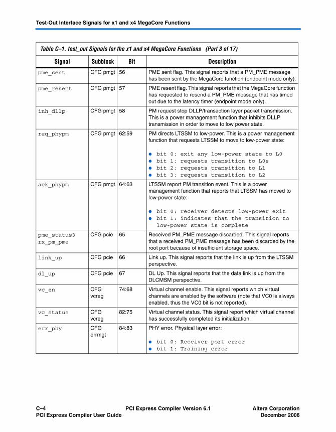
Test-Out Interface Signals for x1 and x4 MegaCore Functions
pme_sent CFG pmgt 56 PME sent flag. This signal reports that a PM_PME message has been sent by the MegaCore function (endpoint mode only).
pme_resent CFG pmgt 57 PME resent flag. This signal reports that the MegaCore function has requested to resend a PM_PME message that has timed out due to the latency timer (endpoint mode only).
inh_dllp CFG pmgt 58 PM request stop DLLP/transaction layer packet transmission. This is a power management function that inhibits DLLP transmission in order to move to low power state.
req_phypm CFG pmgt 62:59 PM directs LTSSM to low-power. This is a power management function that requests LTSSM to move to low-power state:
● bit 0: exit any low-power state to L0● bit 1: requests transition to L0s● bit 2: requests transition to L1● bit 3: requests transition to L2
ack_phypm CFG pmgt 64:63 LTSSM report PM transition event. This is a power management function that reports that LTSSM has moved to low-power state:
● bit 0: receiver detects low-power exit● bit 1: indicates that the transition to
low-power state is complete
pme_status3rx_pm_pme
CFG pcie 65 Received PM_PME message discarded. This signal reports that a received PM_PME message has been discarded by the root port because of insufficient storage space.
link_up CFG pcie 66 Link up. This signal reports that the link is up from the LTSSM perspective.
dl_up CFG pcie 67 DL Up. This signal reports that the data link is up from the DLCMSM perspective.
vc_en CFG vcreg
74:68 Virtual channel enable. This signal reports which virtual channels are enabled by the software (note that VC0 is always enabled, thus the VC0 bit is not reported).
vc_status CFG vcreg
82:75 Virtual channel status. This signal report which virtual channel has successfully completed its initialization.
err_phy CFG errmgt
84:83 PHY error. Physical layer error:
● bit 0: Receiver port error● bit 1: Training error
Table C–1. test_out Signals for the x1 and x4 MegaCore Functions (Part 3 of 17)
Signal Subblock Bit Description
C–4 PCI Express Compiler Version 6.1 Altera CorporationPCI Express Compiler User Guide December 2006

err_dll CFG errmgt
89:85 Data link layer error. Data link layer error:
● bit 0: Transaction layer packet error● bit 1: Data link layerP error● bit 2: Replay timer error● bit 3: Replay counter rollover● bit 4: Data link layer protocol error
err_trn CFG errmgt
98:90 TRN error. Transaction layer error:
● bit 0: Poisoned transaction layer packet received
● bit 1: ECRC check failed● bit 2: Unsupported request● bit 3: Completion timeout● bit 4: Completer abort● bit 5: Unexpected Completion● bit 6: Receiver overflow● bit 7: Flow control protocol error● bit 8: Malformed transaction layer packet
r2c_ackc2r_ackrxbuf_busyrxfc_updated
TRN rxvc0
102:99 Receive VC0 status. Reports different events related to VC0.
● bit 0: Transaction layer packet sent to the configuration space
● bit 1: Transaction layer packet received from configuration space
● bit 2: Receive buffer not empty● bit 3: Receive flow control credits
updated
r2c_ackc2r_ackrxbuf_busyrxfc_updated
TRN rxvc1
106:013 Receive VC1 status. Reports different events related to VC1:
● bit 0: transaction layer packet sent to the configuration space
● bit 1: transaction layer packet received from configuration space
● bit 2: Receive buffer not empty● bit 3: Receive flow control credits
updated
Table C–1. test_out Signals for the x1 and x4 MegaCore Functions (Part 4 of 17)
Signal Subblock Bit Description
Altera Corporation PCI Express Compiler Version 6.1 C–5December 2006 PCI Express Compiler User Guide

Test-Out Interface Signals for x1 and x4 MegaCore Functions
r2c_ackc2r_ackrxbuf_busyrxfc_updated
TRN rxvc2
110:107 Receive VC2 status. Reports different events related to VC2:
● bit 0: transaction layer packet sent to the configuration space
● bit 1: transaction layer packet received from configuration space
● bit 2: Receive buffer not empty● bit 3: Receive flow control credits
updated
r2c_ackc2r_ackrxbuf_busyrxfc_updated
TRN rxvc3
114:111 Receive VC3 status. Reports different events related to VC3:
● bit 0: Transaction layer packet sent to the configuration space
● bit 1: Transaction layer packet received from configuration space
● bit 2: Receive buffer not empty● bit 3: Receive flow control credits
updated
Reserved All consecutive signals between bits 131 and 255 depend on the virtual channel selected by the test_in[31:29] input.
desc_sm TRN rxvc 133:131 Receive descriptor state machine. Receive descriptor state machine encoding:
● 000: idle● 001: desc0● 010: desc1● 011: desc2● 100: desc_wt● others: reserved
desc_val TRN rxvc 134 Receive bypass mode valid. This signal reports that bypass mode is valid for the current received transaction layer packet.
data_sm TRN rxvc 136:135 Receive data state machine. Receive data state machine encoding:
● 00: idle● 01: data_first● 10: data_next● 11: data_last
req_ro TRN rxvc 137 Receive reordering queue busy. This signal reports that transaction layer packets are currently reordered in the reordering queue (information extracted from the transaction layer packet FIFO).
Table C–1. test_out Signals for the x1 and x4 MegaCore Functions (Part 5 of 17)
Signal Subblock Bit Description
C–6 PCI Express Compiler Version 6.1 Altera CorporationPCI Express Compiler User Guide December 2006

tlp_emp TRN rxvc 138 Receive transaction layer packet FIFO empty flag. This signal reports that the transaction layer packet FIFO is empty.
tlp_val TRN rxvc 139 Receive transaction layer packet pending in normal queue. This signal reports that a transaction layer packet has been extracted from the transaction layer packet FIFO, but is still pending for transmission to the application layer.
txbk_sm TRN txvc 143:140 Transmit state machine. Transmit state machine encoding:
● 0000: idle● 0001: desc4dw● 0010: desc3dw_norm● 0011: desc3dw_shft● 0100: data_norm● 0101: data_shft ● 0110: data_last● 0111: config0● 1000: config1● others: reserved
rx_sub TRN rxfc 199:144 Receive flow control credits. Receive buffer current credits available:
● bit [7:0]: Posted Header (PH)● bit [19:8]: Posted Data (PD)● bit [27:20]: Non-Posted Header (NPH)● bit [35:28]: Non-Posted Data (NPD)● bit [43:36]: Completion Header (CPLH)● bit [55:44]: Completion Data (CPLD)
Flow control credits for NPD is limited to 8 bits due to the fact that more NPD credits than NPH credits is meaningless.
tx_sub TRN txfc 255:200 Transmit flow control credits. Transmit buffer current credits available:
● bit [7:0]: Posted Header (PH)● bit [19:8]: Posted Data (PD)● bit [27:20]: Non-Posted Header (NPH)● bit [35:28]: Non-Posted Data (NPD)● bit [43:36]: Completion Header (CPLH)● bit [55:44]: Completion Data (CPLD)
Flow control credits for NPD is limited to 8 bits due to the fact that more NPD credits than NPH credits is meaningless.
Table C–1. test_out Signals for the x1 and x4 MegaCore Functions (Part 6 of 17)
Signal Subblock Bit Description
Altera Corporation PCI Express Compiler Version 6.1 C–7December 2006 PCI Express Compiler User Guide

Test-Out Interface Signals for x1 and x4 MegaCore Functions
dlcm_sm DLL dlcmsm
257:256 DLCM state machine. DLCM state machine encoding:
● 00: dl_inactive● 01: dl_init● 10: dl_active● 11: reserved
fcip_sm DLL dlcmsm
260:258 Transmit InitFC state machine. Transmit Init flow control state encoding:
● 000: idle● 001: prep0● 010: prep1● 011: initfc_p● 100: initfc_np● 101: initfc_cpl● 110: initfc_wt● 111: reserved
rxfc_sm DLL dlcmsm
263:261 Receive InitFC state machine. Receive Init flow control state encoding:
● 000: idle● 001: ifc1_p● 010: ifc1_np● 011: ifc1_cpl● 100: ifc2● 111: reserved
flag_fi1 DLL dlcmsm
264 Flag_fi1. FI1 flag as detailed in the PCI Express™ Base Specification Revision 1.0a
flag_fi2 DLL dlcmsm
265 Flag_fi2. FI2 flag as detailed in the PCI Express™ Base Specification Revision 1.0a
rxfc_sm DLL rtry 268:266 Retry state machine. Retry State Machine encoding:
● 000: idle● 001: rtry_ini● 010: rtry_wt0● 011: rtry_wt1● 100: rtry_req● 101: rtry_tlp● 110: rtry_end● 111: reserved
Table C–1. test_out Signals for the x1 and x4 MegaCore Functions (Part 7 of 17)
Signal Subblock Bit Description
C–8 PCI Express Compiler Version 6.1 Altera CorporationPCI Express Compiler User Guide December 2006

storebuf_sm DLL rtry 270:269 Retry buffer storage state machine. Retry buffer storage state machine encoding:
● 00: idle● 01: rtry● 10: str_tlp● 11: reserved
mem_replay DLL rtry 271 Retry buffer running. This signal keeps track of transaction layer packets that have been sent but not yet acknowledged. The replay timer is also running when this bit is set except if a replay is currently performed.
mem_rtry DLL rtry 272 Memorize replay request. This signal indicates that a replay time-out event has occurred or that a NAK DLLP has been received.
replay_num DLL rtry 274:273 Replay number counter. This signal counts the number of replays performed by the MegaCore function for a particular transaction layer packet (as described in the PCI Express™ Base Specification Revision 1.0a).
val_nak_r DLL rtry 275 ACK/NAK DLLP received. This signal reports that an ACK or a NAK DLLP has been received. The res_nak_r, tlp_ack, err_dl, and no_rtry signals detail the type of ACK/NAK DLLP received.
res_nak_r DLL rtry 276 NAK DLLP parameter. This signal reports that the received ACK/NAK DLLP is NAK.
tlp_ack DLL rtry 277 Real ACK DLLP parameter. This signal reports that the received ACK DLLP acknowledges one or several transaction layer packets in the retry buffer.
err_dl DLL rtry 278 Error ACK/NAK DLLP parameter. This signal reports that the received ACK/NAK DLLP has a sequence number higher than the sequence number of the last transmitted transaction layer packet.
no_rtry DLL rtry 279 No retry on NAK DLLP parameter. This signal reports that the received NAK DLLP sequence number corresponds to the last acknowledged transaction layer packet.
Table C–1. test_out Signals for the x1 and x4 MegaCore Functions (Part 8 of 17)
Signal Subblock Bit Description
Altera Corporation PCI Express Compiler Version 6.1 C–9December 2006 PCI Express Compiler User Guide

Test-Out Interface Signals for x1 and x4 MegaCore Functions
txdl_sm DLL txdl 282:280 Transmit transaction layer packet State Machine. Transmit transaction layer packet state machine encoding:
● 000: idle● 001: tlp1● 010: tlp2● 011: tlp3a● 100: tlp5a (ECRC only)● 101: tlp6a (ECRC only)● 111: reserved
This signal can be used to inject an LCRC or ECRC error.
tx3btx4tx5b
DLL txdl 283 Transaction layer packet transmitted. This signal is set on the last DWORD of the packet where the LCRC is added to the packet.This signal can be used to inject an LCRC or ECRC error.
tx0 DLL txdl 284 DLLP transmitted. This signal is set when a DLLP is sent to the physical layer. This signal can be used to inject a CRC on a DLLP.
gnt DLL txdl 292:285 Data link layer transmit arbitration result. This signal reports the arbitration result between a DLLP and a transaction layer packet:
● bit 0: InitFC DLLP● bit 1: ACK DLLP (high priority)● bit 2: UFC DLLP (high priority)● bit 3: PM DLLP ● bit 4: TXN transaction layer packet● bit 5: RPL transaction layer packet● bit 6: UFC DLLP (low priority)● bit 7: ACK DLLP (low priority)
sop DLL txdl 293 Data link layer to PHY start of packet. This signal reports that an SDP/STP symbol is in transition to the physical layer.
eop DLL txdl 294 Data link layer to PHY end of packet. This signal reports that an EDB/END symbol is in transition to the physical layer.
When sop and eop are transmitted together, it indicates that the packet is a DLLP. Otherwise the packet is a transaction layer packet.
eot DLL txdl 295 Data link layer to PHY end of transmit. This signal reports that the data link layer has finished its previous transmission and enables the physical layer to go to low-power state or to recovery.
Table C–1. test_out Signals for the x1 and x4 MegaCore Functions (Part 9 of 17)
Signal Subblock Bit Description
C–10 PCI Express Compiler Version 6.1 Altera CorporationPCI Express Compiler User Guide December 2006

init_lat_timer DLL rxdl 296 Enable ACK latency timer. This signal reports that the ACK latency timer is running.
req_lat DLL rxdl 297 ACK latency timeout. This signal reports that an ACK/NAK DLLP retransmission has been scheduled due to the ACK latency timer expiring.
tx_req_nak or tx_snd_nak
DLL rxdl 298 ACK/NAK DLLP requested for transmission. This signal reports that an ACK/NAK DLLP is currently requested for transmission.
tx_res_nak DLL rxdl 299 ACK/NAK DLLP type requested for transmission. This signal reports that type of ACK/NAK DLLP scheduled for transmission:
● 0: ACK● 1: NAK
rx_val_pm DLL rxdl 300 Received PM DLLP. This signal reports that a PM DLLP has been received (the specific type is indicated by rx_vcid_fc):
● 000: PM_Enter_L1● 001: PM_Enter_L23● 011: PM_AS_Request_L1● 100: PM_Request_ACK
rx_val_fc DLL rxdl 301 Received flow control DLLP. This signal reports that a PM DLLP has been received. The type of flow control DLLP is indicated by rx_typ_fc and rx_vcid_fc.
rx_typ_fc DLL rxdl 305:302 Received flow control DLLP type parameter. This signal reports the type of received flow control DLLP:
● 0100: InitFC1_P● 0101: InitFC1_NP● 0110: InitFC1_CPL● 1100: InitFC2_P● 1101: InitFC2_NP● 1110: InitFC2_CPL● 1000: UpdateFC_P● 1001: UpdateFC_NP● 1010: UpdateFC_CPL
Table C–1. test_out Signals for the x1 and x4 MegaCore Functions (Part 10 of 17)
Signal Subblock Bit Description
Altera Corporation PCI Express Compiler Version 6.1 C–11December 2006 PCI Express Compiler User Guide

Test-Out Interface Signals for x1 and x4 MegaCore Functions
rx_vcid_fc DLL rxdl 308:306 Received flow control DLLP virtual channel ID parameter. This signal reports the virtual channel ID of the received flow control DLLP:
● 000: VCID 0● 001: VCID 1● …● 111: VCID 7
This signal also indicates the type of PM DLLP received.
crcinv DLL rxdl 309 Received nullified transaction layer packet. This signal indicates that a nullified transaction layer packet has been received.
crcerr DLL rxdl 310 Received transaction layer packet with LCRC error. This signal reports that a transaction layer packet has been received that contains an LCRC error.
crcvaleqseq_r
DLL rxdl 311 Received valid transaction layer packet. This signal reports that a valid transaction layer packet has been received that contains the correct sequence number. Such a transaction layer packet is transmitted to the application layer.
crcval!eqseq_rinfseq_r
DLL rxdl 312 Received duplicated transaction layer packet. This signal indicates that a transaction layer packet has been received that has already been correctly received. Such a transaction layer packet is silently discarded.
crcval!eqseq_r!infseq_r
DLL rxdl 313 Received erroneous transaction layer packet. This signal indicates that a transaction layer packet has been received that contains a valid LCRC but a non-sequential sequence number (higher than the current sequence number).
rx_err_frame DLL dlink 314 Data link layer framing error detected. This signal indicates that received data cannot be considered as a DLLP or transaction layer packet, in which case a Receive Port error is generated and link retraining is initiated.
tlp_count DLL rtry 319:315 transaction layer packet count in retry buffer. This signal indicates the number of transaction layer packets stored in the retry buffer (saturation limit is 31).
Table C–1. test_out Signals for the x1 and x4 MegaCore Functions (Part 11 of 17)
Signal Subblock Bit Description
C–12 PCI Express Compiler Version 6.1 Altera CorporationPCI Express Compiler User Guide December 2006

ltssm_r MAC ltssm
324:320 LTSSM state. LTSSM state encoding:
● 00000: detect.quiet● 00001: detect.active● 00010: polling.active● 00011: polling.compliance● 00100: polling.configuration● 00101: reserved (polling.speed)● 00110: config.linkwidthstart● 00111: config.linkaccept● 01000: config:disable● 01001: config.loopback.entry● 01010: config.loopback.active● 01011: config.loopback.exit● 01100: recovery.rcvlock● 01101: recovery.rcvconfig● 01110: recovery.idle● 01111: L0● 10000: disable● 10001: loopback.entry● 10010: loopback.active● 10011: loopback.exit● 10100: hot.reset● 10101: L0s (transmit only)● 10110: L1.entry● 10111: L1.idle● 11000: L2.idle● 11001: L2.transmit.wake
rxl0s_sm MAC ltssm
326:325 Receive L0s state. Receive L0s state machine:
● 00: inact● 01: idle● 10: fts● 11: out.recovery
txl0s_sm MAC ltssm
329:327 TX L0s state. Transmit L0s state machine:
● 000b: inact● 001b: entry● 010b: idle● 011b: fts● 100b: out.l0
timeout MAC ltssm
330 LTSSM timeout. This signal serves as a flag that indicates that the LTSSM time-out condition has been reached for the current LTSSM state.
Table C–1. test_out Signals for the x1 and x4 MegaCore Functions (Part 12 of 17)
Signal Subblock Bit Description
Altera Corporation PCI Express Compiler Version 6.1 C–13December 2006 PCI Express Compiler User Guide

Test-Out Interface Signals for x1 and x4 MegaCore Functions
txos_end MAC ltssm
331 Transmit LTSSM exit condition. This signal serves as a flag that indicates that the LTSSM exit condition for the next state (to go to L0) has been completed. If the next state is not reached in a timely manner, it is due to a problem on the receiver.
tx_ack MAC ltssm
332 Transmit PLP acknowledge. This signal is active for 1 clock cycle when the requested PLP (physical layer packet) has been sent to the link. The type of packet is defined by the tx_ctrl signal.
tx_ctrl MAC ltssm
335:333 Transmit PLP type. This signal indicates the type of transmitted PLP:
● 000: Electrical Idle● 001: Receiver detect during Electrical
Idle● 010: TS1 OS● 011: TS2 OS● 100: D0.0 idle data● 101: FTS OS● 110: IDL OS● 111: Compliance pattern
txrx_det MAC ltssm
343:336 Receiver detect result. This signal serves as a per lane flag that reports the receiver detection result. The 4 MSB are always zero.
tx_pad MAC ltssm
351:344 Force PAD on transmitted TS pattern. This is a per lane internal signal that force PAD transmission on the link and lane field of the transmitted TS1/TS2 OS. The MegaCore function considers that lanes indicated by this signal should not be initialized during the initialization process.
The 4 MSB are always zero.
rx_ts1 MAC ltssm
359:352 Received TS1: This signal indicates that a TS1 has been received on the specified lane. This signal is cleared when a new state is reached by the LTSSM state machine.
The 4 MSB are always zero.
rx_ts2 MAC ltssm
367:360 Received TS2. This signal indicates that a TS1 has been received on the specified lane. This signal is cleared when a new state is reached by the LTSSM state machine.
The 4 MSB are always zero.
Table C–1. test_out Signals for the x1 and x4 MegaCore Functions (Part 13 of 17)
Signal Subblock Bit Description
C–14 PCI Express Compiler Version 6.1 Altera CorporationPCI Express Compiler User Guide December 2006

rx_8d00 MAC ltssm
375:368 Received 8 D0.0 symbol. This signal indicates that eight consecutive idle data symbols have been received. This signal is meaningful for config.idle and recovery.idle states.
The 4 MSB are always zero.
rx_idl MAC ltssm
383:376 Received IDL OS. This signal indicates that an IDL OS has been received on a per lane basis.
The 4 MSB are always zero.
rx_linkpad MAC ltssm
391:384 Received link pad TS. This signal indicates that the link field of the received TS1/TS2 is set to PAD for the specified lane.
The 4 MSB are always zero.
rx_lanepad MAC ltssm
399:392 Received lane pad TS. This signal indicates that the lane field of the received TS1/TS2 is set to PAD for the specified lane.
The 4 MSB are always zero.
rx_tsnum MAC ltssm
407:400 Received consecutive identical TSNumber. This signal reports the number of consecutive identical TS1/TS2 which have been received with exactly the same parameters since entering this state. When the maximum number is reached, this signal restarts from zero.
This signal corresponds to the lane configured as logical lane 0 (may vary depending on lane reversal).
lane_act MAC ltssm
411:408 Lane active mode. This signal indicates the number of Lanes that have been configured during training:
● 0001: 1 lane● 0010: 2 lanes● 0100: 4 lanes
lane_rev MAC ltssm
415:412 Reserved.
count0 MAC deskew
418:416 Deskew FIFO count lane 0. This signal indicates the number of Words in the deskew FIFO for physical lane 0.
count1 MAC deskew
421:419 Deskew FIFO count lane 1. This signal indicates the number of Words in the deskew FIFO for physical lane 1.
count2 MAC deskew
424:422 Deskew FIFO count lane 2. This signal indicates the number of Words in the deskew FIFO for physical lane 2.
count3 MAC deskew
427:425 Deskew FIFO count lane 3. This signal indicates the number of Words in the deskew FIFO for physical lane 3.
Reserved N/A 439:428 Reserved.
Table C–1. test_out Signals for the x1 and x4 MegaCore Functions (Part 14 of 17)
Signal Subblock Bit Description
Altera Corporation PCI Express Compiler Version 6.1 C–15December 2006 PCI Express Compiler User Guide

Test-Out Interface Signals for x1 and x4 MegaCore Functions
err_deskew MAC deskew
447:440 Deskew FIFO error. This signal indicates whether a deskew error (deskew FIFO overflow) has been detected on a particular physical lane. In such a case, the error is considered a receive port error and retraining of the link is initiated.
The 4 MSBs are hard-wired to zero.
rdusedw0 PCS0 451:448 Elastic buffer counter 0. This signal indicates the number of symbols in the elastic buffer.
Monitoring the elastic buffer counter of each lane can highlight the PPM between the receive clock and transmit clock as well as the skew between lanes. Not meaningful when using the generic PIPE PHY interface.
rxstatus0 PCS0 454:452 PIPE rxstatus 0. This signal is used to monitor errors detected and reported on a per lane basis. For example:
● 000: Receive data OK● 001: 1 SKP added● 010: 1 SKP removed● 011: Receiver detected● 100: 8B/10B decode error● 101: Elastic buffer overflow● 110: Elastic buffer underflow● 111: Running disparity error
Not meaningful when using the generic PIPE PHY interface.
rxpolarity0 PCS0 455 PIPE polarity inversion 0. When asserted, the LTSSM requires the PCS subblock to invert the polarity of the received 10-bit data during training.
rdusedw1 PCS1 459:456 Elastic buffer counter 1. This signal indicates the number of symbols in the elastic buffer.
Monitoring the elastic buffer counter of each lane can highlight the PPM between the receive clock and transmit clock as well as the skew between lanes. Not meaningful when using the generic PIPE PHY interface.
Table C–1. test_out Signals for the x1 and x4 MegaCore Functions (Part 15 of 17)
Signal Subblock Bit Description
C–16 PCI Express Compiler Version 6.1 Altera CorporationPCI Express Compiler User Guide December 2006

rxstatus1 PCS1 462:460 PIPE rxstatus 1. This signal is used to monitor errors detected and reported on a per lane basis. For example:
● 000: Receive data OK● 001: 1 SKP added● 010: 1 SKP removed● 011: Receiver detected● 100: 8B/10B decode error● 101: Elastic buffer overflow● 110: Elastic buffer underflow● 111: Running disparity error
Not meaningful when using the generic PIPE PHY interface.
rxpolarity1 PCS1 463 PIPE polarity inversion 1. When asserted, the LTSSM requires the PCS subblock to invert the polarity of the received 10-bit data during training. Not meaningful when using the generic PIPE PHY interface.
rdusedw2 PCS2 467:464 Elastic buffer counter 2. This signal reports the number of symbols in the elastic buffer.
Monitoring the elastic buffer counter of each lane can highlight the PPM between the receive clock and transmit clock as well as the skew between lanes. Not meaningful when using the generic PIPE PHY interface.
rxstatus2 PCS2 470:468 PIPE rxstatus 2. This signal is used to monitor errors detected and reported on a per lane basis. For example:
● 000: receive data OK● 001: 1 SKP added● 010: 1 SKP removed● 011: Receiver detected● 100: 8B/10B decode error● 101: Elastic buffer overflow● 110: Elastic buffer underflow● 111: Running disparity error
Not meaningful when using the generic PIPE PHY interface.
rxpolarity2 PCS2 471 PIPE polarity inversion 2. When asserted, the LTSSM requires the PCS subblock to invert the polarity of the received 10-bit data during training. Not meaningful when using the generic PIPE PHY interface.
Table C–1. test_out Signals for the x1 and x4 MegaCore Functions (Part 16 of 17)
Signal Subblock Bit Description
Altera Corporation PCI Express Compiler Version 6.1 C–17December 2006 PCI Express Compiler User Guide

Test-Out Interface Signals for x1 and x4 MegaCore Functions
rdusedw3 PCS3 475:472 Elastic buffer counter 3. This signal reports the number of symbols in the elastic Buffer.
Monitoring the elastic buffer counter of each lane can highlight the PPM between the receive clock and transmit clock as well as the skew between lanes. Not meaningful when using the generic PIPE PHY interface.
rxstatus3 PCS3 478:476 PIPE rxstatus 3. This signal is used to monitor errors detected and reported on a per lane basis. For example:
● 000: receive data OK● 001: 1 SKP added● 010: 1 SKP removed● 011: Receiver detected● 100: 8B/10B decode error● 101: Elastic buffer overflow● 110: Elastic buffer underflow● 111: Running disparity error
Not meaningful when using the generic PIPE PHY interface.
rxpolarity3 PCS3 479 PIPE polarity inversion 3. When asserted, the LTSSM requires the PCS subblock to invert the polarity of the received 10-bit data during training. Not meaningful when using the generic PIPE PHY interface.
Reserved PCS4 511:480 Reserved.
Table C–1. test_out Signals for the x1 and x4 MegaCore Functions (Part 17 of 17)
Signal Subblock Bit Description
C–18 PCI Express Compiler Version 6.1 Altera CorporationPCI Express Compiler User Guide December 2006

Test-Out Interface Signals for x8 MegaCore Functions
Table C–2 describes the test-out signals for the x8 MegaCore functions.
Table C–2. test_out Signals for the x8 MegaCore Functions (Part 1 of 4)
Signal Subblock Bit Description
ltssm_r MACltssm
4:0 LTSSM state: LTSSM state encoding:00000: detect.quiet00001: detect.active00010: polling.active00011: polling.compliance00100: polling.configuration00110: config.linkwidthstart00111: config.linkaccept01000: config.lanenumaccept01001: config.lanenumwait01010: config.complete01011: config.idle01100: recovery.rcvlock01101: recovery.rcvconfig01110: recovery.idle01111: L010000: disable10001: loopback.entry10010: loopback.active10011: loopback.exit10100: Hot reset10101: L0s10110: L1.entry10111: L1.idle11000: L2.idle11001: L2 transmit.wake
rxl0s_sm MACltssm
6:5 Receive L0s state: Receive L0s state machine00: inact01: idle10: fts11: out.recovery
Altera Corporation PCI Express Compiler Version 6.1 C–19December 2006 PCI Express Compiler User Guide

Test-Out Interface Signals for x8 MegaCore Functions
txl0s_sm MACltssm
9:7 TX L0s state: Transmit L0s state machine000b: inact001b: entry010b: idle011b: fts100b: out.l0
timeout MACltssm
10 LTSSM Timeout: This signal serves as a flag that indicates that the LTSSM timeout condition has been reached for the current LTSSM state.
txos_end MACltssm
11 Transmit LTSSM exit condition: This signal serves as a flag that indicates that the LTSSM exit condition for the next state (in order to go to L0) has been completed. If the next state is not reached in a timely manner, it is due to a problem on the receiver.
tx_ack MACltssm
12 Transmit PLP acknowledge: This signal is active for 1 clock cycle when the requested PLP (Physical Layer Packet) has been sent to the Link. The type of packet is defined by TX_CTRL.
tx_ctrl MACltssm
15:13 Transmit PLP type: This signal000: Electrical Idle001: Receiver detect during010: TS1 OS011: TS2 OS100: D0.0 idle data101: FTS OS110: IDL OS111: Compliance pattern
txrx_det MACltssm
23:16 Receiver detect result: This signal serves as a per-lane flag that reports the receiver detection result.
tx_pad MACltssm
31:24 Force PAD on transmitted TS pattern: This is a per-lane internal signal that force PAD transmission on the Link and lane field of the transmitted TS1/TS2 OS. The Core considers that Lanes indicated by this signal should not be initialized during the initialization process.
rx_ts1 MACltssm
39:32 Received TS1: This signal indicates that a TS1 has been received on the specified Lane. This signal is cleared when a new state is reached by the LTSSM state machine.
rx_ts2 MACltssm
47:40 Received TS2: This signal indicates that a TS1 has been received on the specified Lane. This signal is cleared when a new state is reached by the LTSSM state machine.
Table C–2. test_out Signals for the x8 MegaCore Functions (Part 2 of 4)
Signal Subblock Bit Description
C–20 PCI Express Compiler Version 6.1 Altera CorporationPCI Express Compiler User Guide December 2006

rx_8d00 MACltssm
55:48 Received 8 D0.0 symbol: This signal indicates that eight consecutive Idle data symbols have been received. This signal is meaningful for config.idle and recovery.idle states.
rx_idl MACltssm
63:56 Received 8 D0.0 symbol: This signal indicates that eight consecutive Idle data symbols have been received. This signal is meaningful for config.idle and recovery.idle states.
rx_linkpad MACltssm
71:64 Received Link Pad TS: This signal indicates that the Link field of the received TS1/TS2 is set to PAD for the specified lane.
rx_lanepad MACltssm
79:72 Received Lane Pad TS: This signal indicates that the Lane field of the received TS1/TS2 is set to PAD for the specified lane.
rx_tsnum MACltssm
87:80 Received Consecutive Identical TSNumber: This signal reports the number of consecutive identical TS1/TS2 which have been received with exactly the same parameters since entering this state. When the maximum number is reached, this signal restarts from zero. Note that this signal corresponds to the lane configured as logical lane 0.
lane_act MACltssm
91:88 Lane Active Mode: This signal indicates the number of Lanes that have been configured during training:
0001: 1 lane0010: 2 lanes0100: 4 lanes1000: 8 lanes
lane_rev MACltssm
95:92 Reserved
count0 MACdeskew
98:96 Deskew fifo count lane 0: This signal indicates the number of Words in the deskew fifo for physical lane 0.
count1 MACdeskew
101:99 Deskew fifo count lane 1: This signal indicates the number of Words in the deskew fifo for physical lane 1.
count2 MACdeskew
104:102 Deskew fifo count lane 2: This signal indicates the number of Words in the deskew fifo for physical lane 2.
count3 MACdeskew
107:105 Deskew fifo count lane 3: This signal indicates the number of Words in the deskew fifo for physical lane 3.
count4 MACdeskew
110:108 Deskew fifo count lane 4: This signal indicates the number of Words in the deskew fifo for physical lane 4.
count5 MACdeskew
113:111 Deskew fifo count lane 5:This signal indicates the number of Words in the deskew fifo for physical lane 5.
Table C–2. test_out Signals for the x8 MegaCore Functions (Part 3 of 4)
Signal Subblock Bit Description
Altera Corporation PCI Express Compiler Version 6.1 C–21December 2006 PCI Express Compiler User Guide

Test-In Interface
Test-In Interface You must implement specific logic in order to use the error-injection capabilities of the test_in port. For example, to force an LCRC error on the next transmitted transaction layer packet, test_in[21] must be asserted for 1 clock cycle when transmit txdl_sm, (test_out[282:280]) is in a non-idle state.
Table C–3 describes test_in signals.
count6 MACdeskew
116:114 Deskew fifo count lane 6: This signal indicates the number of Words in the deskew fifo for physical lane 6.
count7 MACdeskew
119:117 Deskew fifo count lane 7: This signal indicates the number of Words in the deskew fifo for physical lane 7.
err_deskew MACdeskew
127:120 Deskew fifo error: This signal indicates whether a deskew error (deskew fifo overflow) has been detected on a particular physical Lane. In such a case, the error is considered a Receive Port error and retraining of the Link is initiated.
Table C–2. test_out Signals for the x8 MegaCore Functions (Part 4 of 4)
Signal Subblock Bit Description
Table C–3. test_in Signals (Part 1 of 5)
Signal Subblock Bit Description
test_sim MAC ltssm 0 Simulation mode. This signal must be set to 1 to accelerate MegaCore function initialization.
test_lpbk MAC ltssm 1 Loopback master. This signal must be set to 1 to direct the link to loopback (in master mode). This bit is reserved on the x8 MegaCore function.
test_discr MAC ltssm 2 Descramble mode. This signal must be set to 1 during initialization to disable data scrambling.
test_nonc_phy MAC ltssm 3 Force_rxdet mode. This signal can be set to 1 in cases where the PHY implementation does not support the Rx Detect feature. The MegaCore function always detects the maximum number of receivers during the detect state, and only goes to compliance state if at least one lane has the correct pattern. This signal is forced internal to the MegaCore function for Stratix GX PHY implementations.
test_boot CFGcfgchk 4 Remote boot mode. When asserted, this signal disables the BAR check if the link is not initialized and the boot is located behind the component.
C–22 PCI Express Compiler Version 6.1 Altera CorporationPCI Express Compiler User Guide December 2006

test_compliance MAC ltssm 6:5 Compliance test mode. Disable/force compliance mode:
● bit 0 completely disables compliance mode.● bit 1 forces compliance mode.
test_pwr CFG PMGT
7 Disable low power state negotiation. When asserted, this signal disables all low power state negotiation and entry. This mode can be used when the attached PHY does not support the electrical idle feature used in low-power link states. The MegaCore function will not attempt to place the link in Tx L0s state or L1 state when this bit is asserted. For Stratix GX PHY implementations, this bit is forced to a 1 internal to the MegaCore function.
test_pcserror PCS 13:8 Lane error injection. Disable/force compliance mode. The first three bits indicate the following modes:
● test_pcserror[2:0]: 000: normal mode● test_pcserror[2:0]: 001: inject data error● test_pcserror[2:0]: 010: inject disparity
error● test_pcserror[2:0]: 011: inject different
data● test_pcserror[2:0]: 100: inject SDP instead
of END● test_pcserror[2:0]: 101: inject STP instead
of END● test_pcserror[2:0]: 110: inject END instead
of data● test_pcserror[2:0]: 111: inject EDB instead
of END
The last three bits indicate the lane:
● test_pcserror[5:3]: 000: on lane 0● test_pcserror[5:3]: 001: on lane 1● test_pcserror[5:3]: 010: on lane 2● test_pcserror[5:3]: 011: on lane 3
test_rxerrtlp DLL 14 Force transaction layer packet LCRC error detection. When asserted, this signal forces the MegaCore function to treat the next received transaction layer packet as if it had an LCRC error. These bits are reserved on the x8 MegaCore function.
Table C–3. test_in Signals (Part 2 of 5)
Signal Subblock Bit Description
Altera Corporation PCI Express Compiler Version 6.1 C–23December 2006 PCI Express Compiler User Guide

Test-In Interface
test_rxerrdllp DLL 16:15 Force DLLP CRC error detection. This signal forces the MegaCore function to check the next DLLP for a CRC error:
● 00: normal mode● 01: ACK/NAK● 10: PM● 11: flow control These bits are reserved on
the x8 MegaCore function.
test_replay DLL 17 Force retry buffer. When asserted, this signal forces the retry buffer to initiate a retry. These bits are reserved on the x8 MegaCore function.
test_acknak DLL 19:18 Replace ACK by NAK. This signal replaces an ACK by a NAK with following sequence number:
● 00: normal mode● 01: Same sequence number as the ACK● 10: Sequence number incremented● 11: Sequence number decremented
If unused, these bits should be hard-wired to 0 to remove unused logic. These bits are reserved on the x8 MegaCore function.
test_ecrcerr DLL 20 Inject ECRC error on transmission. When asserted, this signal generates an ECRC error for transmission.
test_lcrcerr DLL 21 Inject LCRC error on transmission. When asserted, this signal generates an LCRC error for transmission. These bits are reserved on the x8 MegaCore function.
test_crcerr DLL 23:22 Inject DLLP CRC error on transmission. Generates a CRC error when transmitting a DLLP:
● 00: normal● 01: PM error● 10: flow control error● 11: ACK error
If unused, these bits should be hard-wired to 0 to remove unused logic. These bits are reserved on the x8 MegaCore function.
Table C–3. test_in Signals (Part 3 of 5)
Signal Subblock Bit Description
C–24 PCI Express Compiler Version 6.1 Altera CorporationPCI Express Compiler User Guide December 2006

test_ufcvalue TRN 28:24 Generate wrong value for update flow control. This signal forces an incorrect value when updating flow control credits. It does so by adding or removing one credit in the credits allocated field when a transaction layer packet is extracted from the receive buffer and sent to the application layer:
● 00000: normal mode● 00001: UFC_P error on header (+1/0)● 00010: UFC_P error on data (0/+1)● 00011: UFC_P error on header/data (+1/+1)● 00100: UFC_NP error on header (+1/0)● 00101: UFC_NP error on data (0/+1)● 00110: UFC_NP error on header/data (+1/+1)● 00111: UFC_CPL error on header (+1/0)● 01000: UFC_CPL error on data (0/+1)● 01001: UFC_CPL error header/data (+1/+1)● 01010: UFC_P error on header (-1/0)● 01011: UFC_P error on data (0/-1)● 01100: UFC_P error on header/data (-1/-1)● 01101: UFC_NP error on header (-1/0)● 01110: UFC_NP error on data (0/-1)● 01111: UFC_NP error on header/data (-1/-1)● 10000: UFC_CPL error on header (-1/0)● 10001: UFC_CPL error on data (0/-1)● 10010: UFC_CPL error header/data (-1/-1)● 10011: UFC_P error on header/data (+1/-1)● 10100: UFC_P error on header/data (-1/+1)● 10101: UFC_NP error on header/data (+1/-1)● 10110: UFC_NP error on header/data (-1/+1)● 10111: UFC_CPL error header/data (+1/-1)● 11000: UFC_CPL error header/data (-1/+1)
If unused, these bits should be hard-wired to 0 to remove unused logic. These bits are reserved on the x8 MegaCore function.
Table C–3. test_in Signals (Part 4 of 5)
Signal Subblock Bit Description
Altera Corporation PCI Express Compiler Version 6.1 C–25December 2006 PCI Express Compiler User Guide

Test-In Interface
test_vcselect TRN 31:29 Virtual channel test selection. This signal indicates which virtual channel is currently considered by the test-out interface (test_out[255:131]). This virtual channel test selection is the select input to a mux that switches a portion of the test_out bus to output debug signals from different virtual channels (VC). For example:
● test_vcselect[31:29]:000:test_out[255:131] describes activity for VC0
● test_vcselect[31:29]:001:test_out[255:131] describes activity for VC1
● test_vcselect[31:29]:010:test_out[255:131] describes activity for VC2
● ...
Certain bits of this signal should be set to 0 to remove unused logic:
● 1 virtual channel (or signal completely unused): set all three bits to 000
● 2 virtual channels: set the 2 MSBs to 00● 3 or 4 virtual channels: set the MSB to 0. These bits are
reserved on the x8 MegaCore function.
Table C–3. test_in Signals (Part 5 of 5)
Signal Subblock Bit Description
C–26 PCI Express Compiler Version 6.1 Altera CorporationPCI Express Compiler User Guide December 2006