
PCI Express Card Electromechanical Specification …PCI EXPRESS CARD ELECTROMECHANICAL...
96
PCI Express ™ Card Electromechanical Specification Revision 1.1 March 28 January 24 , 2005
Transcript of PCI Express Card Electromechanical Specification …PCI EXPRESS CARD ELECTROMECHANICAL...
PCI Express™
Card Electromechanical Specification Revision 1.1
March 28January 24, 2005
PCI EXPRESS CARD ELECTROMECHANICAL SPECIFICATION, REV 1.1
2
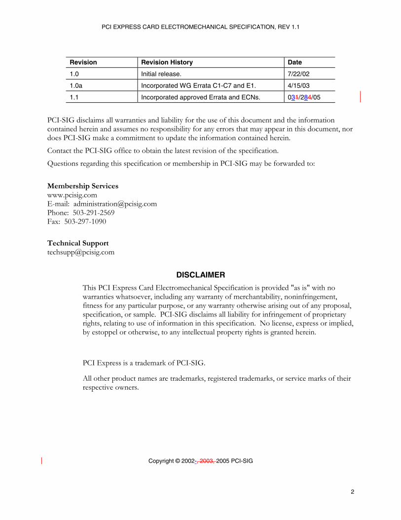
Revision Revision History Date
1.0 Initial release. 7/22/02
1.0a Incorporated WG Errata C1-C7 and E1. 4/15/03
1.1 Incorporated approved Errata and ECNs. 031/284/05
PCI-SIG disclaims all warranties and liability for the use of this document and the information contained herein and assumes no responsibility for any errors that may appear in this document, nor does PCI-SIG make a commitment to update the information contained herein.
Contact the PCI-SIG office to obtain the latest revision of the specification.
Questions regarding this specification or membership in PCI-SIG may be forwarded to:
Membership Services www.pcisig.com E-mail: [email protected] Phone: 503-291-2569 Fax: 503-297-1090
Technical Support [email protected]
DISCLAIMER
This PCI Express Card Electromechanical Specification is provided "as is" with no warranties whatsoever, including any warranty of merchantability, noninfringement, fitness for any particular purpose, or any warranty otherwise arising out of any proposal, specification, or sample. PCI-SIG disclaims all liability for infringement of proprietary rights, relating to use of information in this specification. No license, express or implied, by estoppel or otherwise, to any intellectual property rights is granted herein.
PCI Express is a trademark of PCI-SIG.
All other product names are trademarks, registered trademarks, or service marks of their respective owners.
Copyright © 2002-, 2003, 2005 PCI-SIG
PCI EXPRESS CARD ELECTROMECHANICAL SPECIFICATION, REV 1.1
3
Contents
1. INTRODUCTION........................................................................................................7 1.1. TERMS AND DEFINITIONS ........................................................................................ 7 1.2. REFERENCE DOCUMENTS ........................................................................................ 9 1.3. SPECIFICATION CONTENTS...................................................................................... 9 1.4. OBJECTIVES................................................................................................................ 10 1.5. ELECTRICAL OVERVIEW ........................................................................................ 10 1.6. MECHANICAL OVERVIEW ...................................................................................... 11
2. AUXILIARY SIGNALS............................................................................................13 2.1. REFERENCE CLOCK.................................................................................................. 14
2.1.1. Low Voltage Swing, Differential Clocks ....................................................... 14 2.1.2. Spread Spectrum Clocking (SSC).................................................................. 15 2.1.3. REFCLK AC Specifications........................................................................... 16 2.1.4. REFCLK Phase Jitter Specification .............................................................. 20
2.2. PERST# SIGNAL ......................................................................................................... 21 2.2.1. Initial Power-Up (G3 to L0).......................................................................... 21 2.2.2. Power Management States (S0 to S3/S4 to S0) ............................................. 22 2.2.3. Power Down.................................................................................................. 22
2.3. WAKE# SIGNAL ......................................................................................................... 25 2.4. SMBUS (OPTIONAL).................................................................................................. 28
2.4.1. Capacitive Load of High-power SMBus Lines .............................................. 28 2.4.2. Minimum Current Sinking Requirements for SMBus Devices....................... 29 2.4.3. SMBus “Back Powering” Considerations .................................................... 29 2.4.4. Power-on Reset ............................................................................................. 29
2.5. JTAG PINS (OPTIONAL) ............................................................................................ 30 2.6. AUXILIARY SIGNAL PARAMETRIC SPECIFICATIONS...................................... 31
2.6.1. DC Specifications .......................................................................................... 31 2.6.2. AC Specifications .......................................................................................... 32
3. HOT INSERTION AND REMOVAL......................................................................34 3.1. SCOPE 34 3.2. PRESENCE DETECT................................................................................................... 34
ELECTRICAL REQUIREMENTS ...............................................................................38 4.1. POWER SUPPLY REQUIREMENTS ......................................................................... 38 4.2. POWER CONSUMPTION ........................................................................................... 40 4.3. POWER SUPPLY SEQUENCING............................................................................... 41 4.4. POWER SUPPLY DECOUPLING............................................................................... 41 4.5. ELECTRICAL TOPOLOGIES AND LINK DEFINITIONS ....................................... 42
4.5.1. Topologies ..................................................................................................... 42 4.5.2. Link Definition............................................................................................... 44
4.6. ELECTRICAL BUDGETS ........................................................................................... 45 4.6.1. AC Coupling Capacitors ............................................................................... 45 4.6.2. Insertion Loss Values (Voltage Transfer Function) ...................................... 46 4.6.3. Jitter Values................................................................................................... 48 4.6.4. Crosstalk........................................................................................................ 51 4.6.5. Lane-to-Lane Skew........................................................................................ 51
PCI EXPRESS CARD ELECTROMECHANICAL SPECIFICATION, REV 1.1
4
4.6.6. Equalization .................................................................................................. 52 4.6.7. Skew Within the Differential Pair ................................................................. 52
4.7. EYE DIAGRAMS AT THE ADD-IN CARD INTERFACE........................................ 52 4.7.1. Add-in Card Transmitter Path Compliance Eye-Diagram ........................... 53 4.7.2. Add-in Card Minimum Receiver Path Sensitivity Requirements................... 54 4.7.3. System Board Transmitter Path Compliance Eye Diagram.......................... 55 4.7.4. System Board Minimum Receiver Path Sensitivity Requirements................. 58
5. CONNECTOR SPECIFICATION...........................................................................60 5.1. CONNECTOR PINOUT ............................................................................................... 60 5.2. CONNECTOR INTERFACE DEFINITIONS.............................................................. 65 5.3. SIGNAL INTEGRITY REQUIREMENTS AND TEST PROCEDURES ................... 69 5.4. CONNECTOR ENVIRONMENTAL AND OTHER REQUIREMENTS ................... 72
5.4.1. Environmental Requirements ........................................................................ 72 5.4.2. Mechanical Requirements ............................................................................. 74 5.4.3. Current Rating Requirement ......................................................................... 75 5.4.4. Additional Considerations............................................................................. 76
6. ADD-IN CARD FORM FACTORS AND IMPLEMENTATION ........................78 6.1. ADD-IN CARD FORM FACTORS.............................................................................. 78 6.2. CONNECTOR AND ADD-IN CARD LOCATIONS .................................................. 88 6.3. CARD INTEROPERABILITY ..................................................................................... 94
ACKNOWLEDGEMENTS ............................................................................................96
PCI EXPRESS CARD ELECTROMECHANICAL SPECIFICATION, REV 1.1
5
Figures FIGURE 1-1: VERTICAL EDGE-CARD CONNECTOR .................................................... 11 FIGURE 1-3: EXAMPLE OF A SERVER I/O BOARD WITH PCI EXPRESS SLOTS ON A RISER
....................................................................................................................................... 12 FIGURE 2-1: DIFFERENTIAL REFCLK WAVEFORM .................................................... 14 FIGURE 2-3: EXAMPLE REFERENCE CLOCK SOURCE TERMINATION................... 15 FIGURE 2-4: SINGLE-ENDED MEASUREMENT POINTS FOR ABSOLUTE CROSS POINT
AND SWING ................................................................................................................ 17 FIGURE 2-5: SINGLE-ENDED MEASUREMENT POINTS FOR DELTA CROSS POINT18 FIGURE 2-6: SINGLE-ENDED MEASUREMENT POINTS FOR RISE AND FALL TIME
MATCHING.................................................................................................................. 18 FIGURE 2-7: DIFFERENTIAL MEASUREMENT POINTS FOR DUTY CYCLE AND PERIOD
....................................................................................................................................... 18 FIGURE 2-8: DIFFERENTIAL MEASUREMENT POINTS FOR RISE AND FALL TIME18 FIGURE 2-9: DIFFERENTIAL MEASUREMENT POINTS FOR RINGBACK ................ 19 FIGURE 2-10: REFERENCE CLOCK SYSTEM MEASUREMENT POINT AND LOADING
....................................................................................................................................... 19 FIGURE 2-11: POWER UP ................................................................................................... 21 FIGURE 2-13: POWER MANAGEMENT STATES............................................................ 22 FIGURE 2-15: OUT-OF-TOLERANCE THRESHOLD WINDOWS .................................. 23 FIGURE 2-16: POWER DOWN............................................................................................ 24 FIGURE 2-18: WAKE# RISE AND FALL TIME MEASUREMENT POINTS.................. 32 FIGURE 3-1: PRESENCE DETECT IN A HOT-PLUG ENVIRONMENT......................... 35 FIGURE 4-1: PCI EXPRESS ON THE SYSTEM BOARD.................................................. 42 FIGURE 4-3: PCI EXPRESS CONNECTOR ON SYSTEM BOARD WITH AN ADD-IN CARD
....................................................................................................................................... 43 FIGURE 4-5: PCI EXPRESS CONNECTOR ON A RISER CARD WITH AN ADD-IN CARD
....................................................................................................................................... 44 FIGURE 4-7: LINK DEFINITION FOR TWO COMPONENTS ......................................... 45 FIGURE 4-9: EXAMPLE INTERCONNECT TERMINATED AT THE CONNECTOR
INTERFACE ................................................................................................................. 46 FIGURE 4-11: INSERTION LOSS BUDGETS.................................................................... 47 FIGURE 4-13: JITTER BUDGET ......................................................................................... 48 FIGURE 4-15: ADD-IN CARD TRANSMITTER PATH COMPLIANCE EYE DIAGRAM54 FIGURE 4-17: REPRESENTATIVE COMPOSITE EYE DIAGRAM FOR ADD-IN CARD
RECEIVER PATH COMPLIANCE ............................................................................. 55 FIGURE 4-19: SYSTEM BOARD TRANSMITTER PATH COMPOSITE COMPLIANCE EYE
DIAGRAM.................................................................................................................... 56 FIGURE 4-21: TWO-PORT MEASUREMENT MODEL .................................................... 57 FIGURE 4-22: REPRESENTATIVE COMPOSITE EYE DIAGRAM FOR SYSTEM BOARD
RECEIVER PATH COMPLIANCE ............................................................................. 59 FIGURE 5-1: CONNECTOR FORM FACTOR.................................................................... 65 FIGURE 5-3: RECOMMENDED FOOTPRINT................................................................... 66 FIGURE 5-5: ADD-IN CARD EDGE-FINGER DIMENSIONS.......................................... 67 FIGURE 5-7: ILLUSTRATION OF ADJACENT PAIRS .................................................... 72 FIGURE 5-9: CONTACT RESISTANCE MEASUREMENT POINTS............................... 73 FIGURE 6-1: STANDARD HEIGHT PCI EXPRESS ADD-IN CARD WITHOUT THE I/O
BRACKET .................................................................................................................... 79
PCI EXPRESS CARD ELECTROMECHANICAL SPECIFICATION, REV 1.1
6
FIGURE 6-3: STANDARD HEIGHT PCI EXPRESS ADD-IN CARD WITH THE I/O BRACKET AND CARD RETAINER.............................................................................................. 80
FIGURE 6-5: ADDITIONAL FEATURE AND KEEPOUTS ON THE X16 GRAPHICS CARD....................................................................................................................................... 81
FIGURE 6-6: STANDARD ADD-IN CARD I/O BRACKET .............................................. 82 FIGURE 6-8: BRACKET DESIGN WITH THE MOUNTING TABS MOUNTED ON THE
PRIMARY SIDE OF THE ADD-IN CARD................................................................. 83 FIGURE 6-10: ADD-IN CARD RETAINER ........................................................................ 84 FIGURE 6-12: LOW PROFILE PCI EXPRESS ADD-IN CARD WITHOUT THE I/O BRACKET
....................................................................................................................................... 85 FIGURE 6-14: LOW PROFILE PCI EXPRESS ADD-IN CARD WITH THE I/O BRACKET
....................................................................................................................................... 86 FIGURE 6-16: LOW PROFILE I/O BRACKET................................................................... 87 FIGURE 6-18: EXAMPLE OF A PC SYSTEM IN MICROATX FORM FACTOR ........... 88 FIGURE 6-20: INTRODUCTION OF A PCI EXPRESS CONNECTOR IN A MICROATX
SYSTEM ....................................................................................................................... 89 FIGURE 6-22: MORE PCI EXPRESS CONNECTORS ARE INTRODUCED ON A MICROATX
SYSTEM BOARD ........................................................................................................ 90 FIGURE 6-24: PCI EXPRESS CONNECTOR LOCATION IN A MICROATX SYSTEM WITH
ONE PCI EXPRESS CONNECTOR ............................................................................ 91 FIGURE 6-26: PCI EXPRESS CONNECTOR LOCATION IN A MICROATX SYSTEM WITH
TWO PCI EXPRESS CONNECTORS ......................................................................... 92 FIGURE 6-28: CARD ASSEMBLED IN CONNECTOR..................................................... 93
Tables TABLE 2-1: REFCLCK DC SPECIFICATIONS AND AC TIMING REQUIREMENTS .. 16 TABLE 2-3: AUXILIARY SIGNAL DC SPECIFICATIONS - PERST#, WAKE#, AND SMBUS
....................................................................................................................................... 31 TABLE 2-5: POWER SEQUENCING AND RESET SIGNAL TIMINGS .......................... 32 TABLE 4-1: POWER SUPPLY RAIL REQUIREMENTS................................................... 38 TABLE 4-3: ADD-IN CARD POWER DISSIPATION........................................................ 40 TABLE 4-5: ALLOCATION OF INTERCONNECT PATH INSERTION LOSS BUDGET47 TABLE 4-7: TOTAL SYSTEM JITTER BUDGET.............................................................. 49 TABLE 4-8: ALLOCATION OF INTERCONNECT JITTER BUDGET ............................ 50 TABLE 4-10: ALLOWABLE INTERCONNECT LANE-TO-LANE SKEW...................... 52 TABLE 4-12: ADD-IN CARD TRANSMITTER PATH COMPLIANCE EYE REQUIREMENTS
....................................................................................................................................... 53 TABLE 4-14: ADD-IN CARD MINIMUM RECEIVER PATH SENSITIVITY REQUIREMENTS
....................................................................................................................................... 54 TABLE 5-1: PCI EXPRESS CONNECTORS PINOUT ....................................................... 60 TABLE 5-3: SIGNAL INTEGRITY REQUIREMENTS AND TEST PROCEDURES ....... 70 TABLE 5-5: TEST DURATIONS ......................................................................................... 73 TABLE 5-7: MECHANICAL TEST PROCEDURES AND REQUIREMENTS ................. 74 TABLE 5-9: END OF LIFE CURRENT RATING TEST SEQUENCE ............................... 75 TABLE 5-11: ADDITIONAL REQUIREMENTS ................................................................ 76 TABLE 6-1: ADD-IN CARD SIZES..................................................................................... 78 TABLE 6-3: CARD INTEROPERABILITY......................................................................... 94

PCI EXPRESS CARD ELECTROMECHANICAL SPECIFICATION, REV 1.1
7
1. Introduction This specification is a companion for the PCI Express Base Specification, Revision 1.1. Its primary focus is the implementation of an evolutionary strategy with the current PCI desktop/server mechanical and electrical specifications. The discussions are confined to ATX or ATX-based form factors. Other form factors, such as Mini-PCI Express Mini Card are covered in other separate 5 specifications.
1.1. Terms and Definitions Add-in card A card that is plugged into a connector and mounted in a chassis slot.
ATX A system board form factor. Refer to the ATX Specification, 10 Revision. 2.2. ATX-based form factor Refers to the form factor that does not exactly conform to the ATX specification, but uses the key features of the ATX, such as the slot spacing, I/O panel definition, etc.
Auxiliary signals Signals not required by the PCI Express architecture but necessary 15 for certain desired functions or system implementation, for example, the SMBus signals.
Basic bandwidth Contains one PCI Express Lane.
x1, x4, x8, x16 x1 refers to one PCI Express Lane of basic bandwidth; x4 refers to a collection of four PCI Express Lanes; etc. 20
Down-plugging Plugging a larger Link card into a smaller Link connector;, for example, plugging a x4 card into a x1 connector
Down-shifting Plugging a PCI Express card into a connector that is not fully routed for all of the PCI Express Lanes. For example, plugging an x4 card into an x8 capable connector with only four Lanes 25 being routed.
Evolutionary strategy A strategy to develop the PCI Express connector and card form factors within today’s chassis and system board form factor infrastructure constraints.
High bandwidth Supports larger number of PCI Express Lanes, such as a x16 card 30 or connector.
1

PCI EXPRESS CARD ELECTROMECHANICAL SPECIFICATION, REV 1.1
8
Hot-Plug Insertion and/or removal of a card into an active backplane or system board as defined in PCI Standard Hot-Plug Controller and Subsystem Specification, Revision. 1.0. No special card support is required.
Hot swap Insertion and/or removal of a card into a passive backplane. The card must satisfy specific requirements to support Hot swap. 5
Interoperability Ability to plug a PCI Express card into different Link connectors and the system works, for example, plugging a x1 PCI Express I/O card into a x16 graphics slot.
Link A collection of one or more PCI Express Lanes
Low profile card An add-in card whose height is no more than 68.90 mm 10 (2.731 inches)
microATX An ATX-based system board form factor. Refer to the microATX Motherboard Interface Specification,Revision 1.2. Mini PCI ExpressMini Card PCI Express for mobile form factor, similar to Mini PCI. 15
PCI Express Lane One PCI Express Lane contains two differential lines for Transmitter and two differential lines for Receiver. A by-N Link is composed of N Lanes.
sideband signaling A method for signaling events and conditions using physical signals separate from signals forming the Link between two 20 components.
Standard height card An add-in card whose height is no more than 111.15 mm (4.376 inches)
Up-plugging Plug a smaller Link card into a larger Link connector;. For for example, plugging a x1 card into a x4 connector 25
wakeup A mechanism used by a component to request the reapplication of main power when in the L2 Link state. Two such mechanisms are defined in the PCI Express Base Specification, Revision 1.1: Beacon and WAKE#. This specification requires the use of WAKE# on any add-in card 30 or system board that supports wakeup functionality.

PCI EXPRESS CARD ELECTROMECHANICAL SPECIFICATION, REV 1.1
9
1.2. Reference Documents This specification references the following documents:
PCI Express Base Specification, Revision 1.10 PCI Local Bus Specification, Revision 3.02.3 PCI Express Jitter Modeling 5
PCI Express Jitter and BER ATX Specification, Revision 2.2 MicroATX microATX Motherboard Interface Specification, Revision 1.20 SMBus Specification, Revision 2.0 JTAG Specification (IEEE1149.1) 10
PCI Standard Hot-Plug Controller and Subsystem Specification, Revision 1.0. Compact PCI Hot Swap Specification EIA-364-1000.01: Environmental Test Methodology for Assessing the Performance of Electrical Connectors
and Sockets Used in Business Office Applications EIA-364: Electrical Connector/Socket Test Procedures Including Environmental Classifications 15
1.3. Specification Contents This specification contains the following information:
Auxiliary signals
Add-in card hot insertion and removal
Power delivery 20
Add-in card electrical budget
Connector specification
Card form factors and implementation
PCI EXPRESS CARD ELECTROMECHANICAL SPECIFICATION, REV 1.1
10
1.4. Objectives The objectives of this specification are:
Support 2.5 Gb/s data rate (per direction) with headroom for future bandwidth increases
Enable Hot-Plug and hot swap where they are needed
Leverage desktop and server commonality 5
Facilitate smooth transitions
Allow co-existence of both PCI and PCI Express add-in cards
No chassis or other PC infrastructure changes
Forward looking for future scalability
Extensible for future bandwidth needs 10
Allows future evolution of PC architecture
Maximize card interoperability for user flexibility
Low cost
1.5. Electrical Overview The electrical part of this specification covers auxiliary signals, hot insertion and removal, power 15 delivery, and add-in card interconnect electrical budgets for the evolutionary strategy. The PCI Express Transmitter and Receiver electrical requirements are specified in the PCI Express Base Specification, Revision 1.1..
Besides the signals that are required to transmit/receive data on the PCI Express interface, there are also signals that may be necessary to implement the PCI Express interface in a system environment, 20 or to provide certain desired functions. These signals are referred to as the auxiliary signals. They include:
Reference clock (REFCLK), must be supplied by the system (see Section 2.1.1)
Add-in card presence detect pins (PRSNT1# and PRSNT2#), required
PERST#, required 25
JTAG, optional
SMBus, optional
Wake (WAKE#), required only if the device/system supports wakeup
+3.3Vaux, optional
REFCLK, JTAG, SMBus, PERST#, and WAKE# are described in Chapter 2, ; +3.3Vaux is 30 described in Chapter 4, ; and PRSNT1# and PRSNT2# are described in Chapter 3.
PCI EXPRESS CARD ELECTROMECHANICAL SPECIFICATION, REV 1.1
11
Both Hot-Plug and hot swap of PCI Express add-in cards are supported, but their implementation is optional. Hot-Plug is supported with the evolutionary add-in card form factor. Hot swap is supported with other form factors and will be described in other specifications.
To support Hot-Plug, presence detect pins (PRSNT1# and PRSNT2#) are defined in each end of the connectors and add-in cards. Those presence detect pins are staggered on the add-in cards such 5 that they are last-mate and first-break, detecting the presence of the add-in cards. Chapter 3 discusses the detailed implementation of PCI Express Hot-Plug.
Chapter 4 specifies the PCI Express add-in card electrical requirements, which include power delivery and interconnect electrical budgets. Power is delivered to the PCI Express add-in cards via add-in card connectors, using three voltage rails: +3.3V, +3.3Vaux, and +12V. Note that the 10 +3.3Vaux voltage rail is not required for all platforms (refer to Section 4.1 for more information on the required usage of 3.3Vaux). The maximum add-in card power definitions are based on the card size and Link widths, and are described in Section 4.2. Chapter 4 describes the interconnect electrical budgets, focusing on the add-in card loss and jitter requirements.
1.6. Mechanical Overview 15
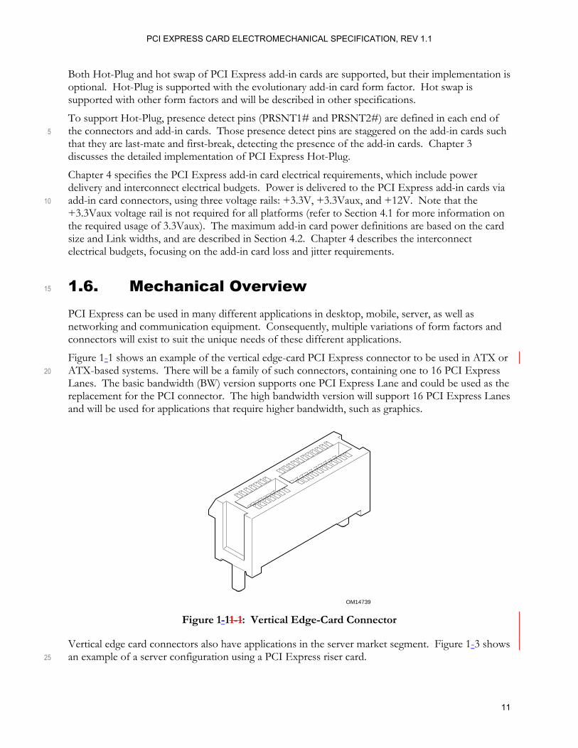
PCI Express can be used in many different applications in desktop, mobile, server, as well as networking and communication equipment. Consequently, multiple variations of form factors and connectors will exist to suit the unique needs of these different applications.
Figure 1-1 shows an example of the vertical edge-card PCI Express connector to be used in ATX or ATX-based systems. There will be a family of such connectors, containing one to 16 PCI Express 20 Lanes. The basic bandwidth (BW) version supports one PCI Express Lane and could be used as the replacement for the PCI connector. The high bandwidth version will support 16 PCI Express Lanes and will be used for applications that require higher bandwidth, such as graphics.
OM14739 Figure 1-11-1: Vertical Edge-Card Connector
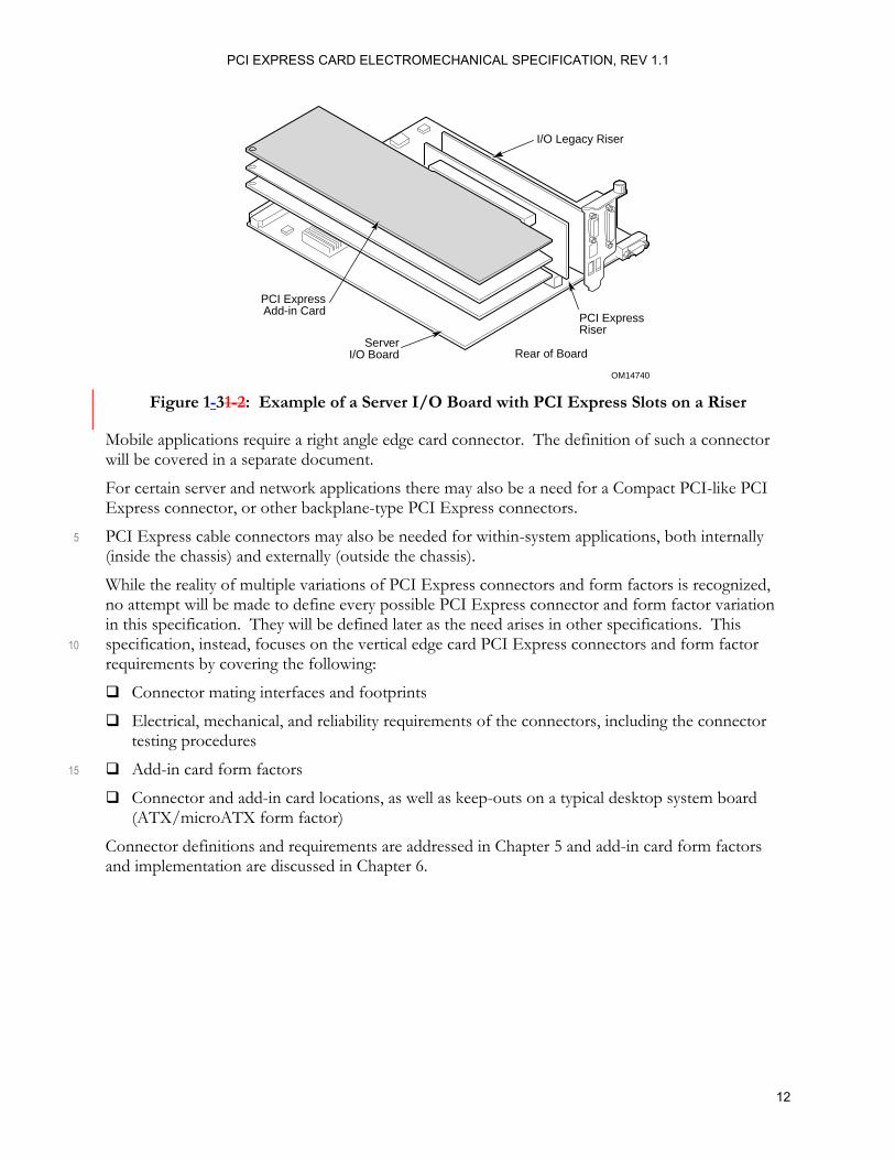
Vertical edge card connectors also have applications in the server market segment. Figure 1-3 shows an example of a server configuration using a PCI Express riser card. 25
PCI EXPRESS CARD ELECTROMECHANICAL SPECIFICATION, REV 1.1
12
I/O Legacy Riser
PCI ExpressRiser
Rear of BoardServer
I/O Board
PCI ExpressAdd-in Card
OM14740 Figure 1-31-2: Example of a Server I/O Board with PCI Express Slots on a Riser
Mobile applications require a right angle edge card connector. The definition of such a connector will be covered in a separate document.
For certain server and network applications there may also be a need for a Compact PCI-like PCI Express connector, or other backplane-type PCI Express connectors.
PCI Express cable connectors may also be needed for within-system applications, both internally 5 (inside the chassis) and externally (outside the chassis).
While the reality of multiple variations of PCI Express connectors and form factors is recognized, no attempt will be made to define every possible PCI Express connector and form factor variation in this specification. They will be defined later as the need arises in other specifications. This specification, instead, focuses on the vertical edge card PCI Express connectors and form factor 10 requirements by covering the following:
Connector mating interfaces and footprints
Electrical, mechanical, and reliability requirements of the connectors, including the connector testing procedures
Add-in card form factors 15
Connector and add-in card locations, as well as keep-outs on a typical desktop system board (ATX/microATX form factor)
Connector definitions and requirements are addressed in Chapter 5 and add-in card form factors and implementation are discussed in Chapter 6.
PCI EXPRESS CARD ELECTROMECHANICAL SPECIFICATION, REV 1.1
13
2. Auxiliary Signals The auxiliary signals are provided on the connector to assist with certain system level functionality or implementation. These signals are not required by the PCI Express architecture. The high-speed signal voltage levels are compatible with advanced silicon processes. The optional low speed signals are defined to use the +3.3V or +3.3Vaux supplies, as they are the lowest common voltage available. 5 Most ASIC processes have high voltage (thick gate oxide) I/O transistors compatible with 3.3 V. Use of the 3.3 V supply allows PCI Express signaling to be used with existing control bus structures, avoiding a buffered set of signals and bridges between the buses.
The PCI Express connector and add-in card interfaces support the following auxiliary signals:
REFCLK-/REFCLK+ (required): low voltage differential signals. 10
PERST# (required): indicates when the applied main power is within the specified tolerance and stable. PERST# goes inactive after a delay of TPVPERL time from the power rails achieving specified tolerance on power up.
WAKE#: an open-drain, active low signal that is driven low by a PCI Express function to re-activate the PCI Express Link hierarchy’s main power rails and reference clocks. It is required 15 on any add-in card or system board that supports wakeup functionality compliant with this specification.
SMBCLK (optional): the SMBus interface clock signal. It is an open-drain signal.
SMBDAT (optional): the SMBus interface address/data signal. It is an open-drain signal.
JTAG (TRST#, TCLK, TDI, TDO, and TMS) (optional): the pins to support IEEE Standard 20 1149.1, Test Access Port and Boundary Scan Architecture (JTAG). They are included as an optional interface for PCI Express devices. IEEE Standard 1149.1 specifies the rules and permissions for designing an 1149.1-compliant IC.
PRSNT1# (required): Add-in card presence detect pin. See Chapter 3 for a detailed description.
PRSNT2# (required): Add-in card presence detect pin. See Chapter 3 for a detailed description. 25
Note that the SMBus interface pins are collectively optional for both the add-in card and the system board. If the optional management features are implemented, SMBCLK and SMBDAT are both required. Similarly, the JTAG pins are collectively optional. If this test mode is implemented, all the JTAG pins are required. Refer to the PCI Local Bus Specification, Rev. 2.33.0, Section 4.3.3 for additional system requirements related to these signals. 30
2
PCI EXPRESS CARD ELECTROMECHANICAL SPECIFICATION, REV 1.1
14
2.1. Reference Clock
2.1.1. Low Voltage Swing, Differential Clocks
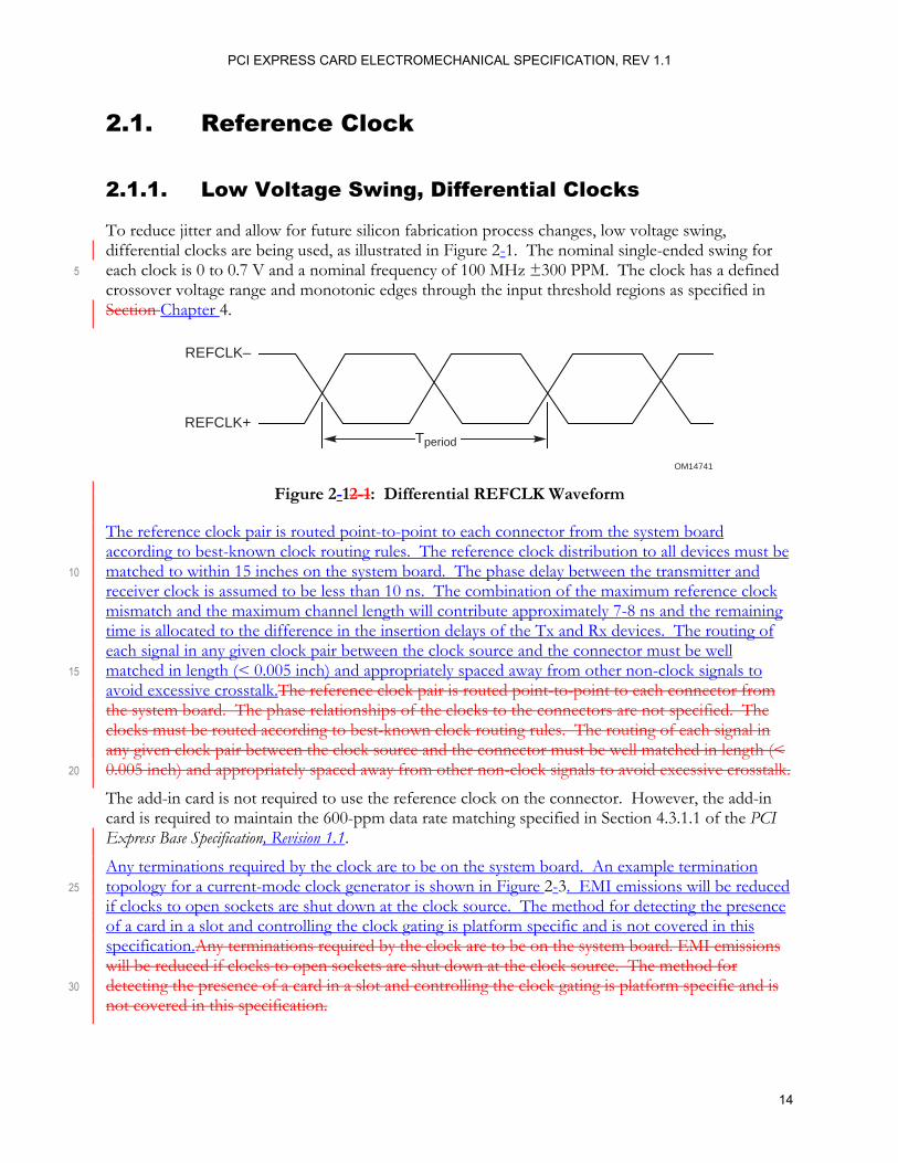
To reduce jitter and allow for future silicon fabrication process changes, low voltage swing, differential clocks are being used, as illustrated in Figure 2-1. The nominal single-ended swing for each clock is 0 to 0.7 V and a nominal frequency of 100 MHz ±300 PPM. The clock has a defined 5 crossover voltage range and monotonic edges through the input threshold regions as specified in Section Chapter 4.
Tperiod
REFCLK–
REFCLK+
OM14741 Figure 2-12-1: Differential REFCLK Waveform
The reference clock pair is routed point-to-point to each connector from the system board according to best-known clock routing rules. The reference clock distribution to all devices must be matched to within 15 inches on the system board. The phase delay between the transmitter and 10 receiver clock is assumed to be less than 10 ns. The combination of the maximum reference clock mismatch and the maximum channel length will contribute approximately 7-8 ns and the remaining time is allocated to the difference in the insertion delays of the Tx and Rx devices. The routing of each signal in any given clock pair between the clock source and the connector must be well matched in length (< 0.005 inch) and appropriately spaced away from other non-clock signals to 15 avoid excessive crosstalk.The reference clock pair is routed point-to-point to each connector from the system board. The phase relationships of the clocks to the connectors are not specified. The clocks must be routed according to best-known clock routing rules. The routing of each signal in any given clock pair between the clock source and the connector must be well matched in length (< 0.005 inch) and appropriately spaced away from other non-clock signals to avoid excessive crosstalk. 20
The add-in card is not required to use the reference clock on the connector. However, the add-in card is required to maintain the 600-ppm data rate matching specified in Section 4.3.1.1 of the PCI Express Base Specification, Revision 1.1.
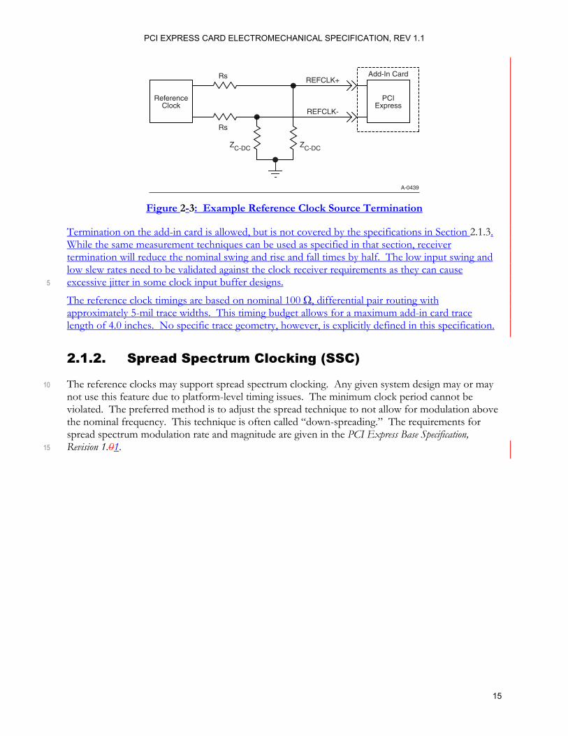
Any terminations required by the clock are to be on the system board. An example termination topology for a current-mode clock generator is shown in Figure 2-3. EMI emissions will be reduced 25 if clocks to open sockets are shut down at the clock source. The method for detecting the presence of a card in a slot and controlling the clock gating is platform specific and is not covered in this specification.Any terminations required by the clock are to be on the system board. EMI emissions will be reduced if clocks to open sockets are shut down at the clock source. The method for detecting the presence of a card in a slot and controlling the clock gating is platform specific and is 30 not covered in this specification.
PCI EXPRESS CARD ELECTROMECHANICAL SPECIFICATION, REV 1.1
15
A-0439
Rs
Rs
ZC-DCZC-DC
ReferenceClock
PCIExpress
Add-In CardREFCLK+
REFCLK-
Figure 2-3: Example Reference Clock Source Termination
Termination on the add-in card is allowed, but is not covered by the specifications in Section 2.1.3. While the same measurement techniques can be used as specified in that section, receiver termination will reduce the nominal swing and rise and fall times by half. The low input swing and low slew rates need to be validated against the clock receiver requirements as they can cause excessive jitter in some clock input buffer designs. 5
The reference clock timings are based on nominal 100 Ω, differential pair routing with approximately 5-mil trace widths. This timing budget allows for a maximum add-in card trace length of 4.0 inches. No specific trace geometry, however, is explicitly defined in this specification.
2.1.2. Spread Spectrum Clocking (SSC)
The reference clocks may support spread spectrum clocking. Any given system design may or may 10 not use this feature due to platform-level timing issues. The minimum clock period cannot be violated. The preferred method is to adjust the spread technique to not allow for modulation above the nominal frequency. This technique is often called “down-spreading.” The requirements for spread spectrum modulation rate and magnitude are given in the PCI Express Base Specification, Revision 1.01. 15

PCI EXPRESS CARD ELECTROMECHANICAL SPECIFICATION, REV 1.1
16
2.1.3. REFCLK AC Specifications
All specifications in Table 2-1 are to be measured using a test configuration as described in Note 11 with a circuit as shown in Figure 2-10.
Table 2-1: REFCLCK DC Specifications and AC Timing Requirements
100 MHz Input Unit Note Symbol Parameter
Min Max
Rise Edge Rate Rising Edge Rate 0.6 4.0 V/ns 2, 3
Fall Edge Rate Falling Edge Rate 0.6 4.0 V/ns 2, 3
VIH Differential Input High Voltage +150 mV 2
VIL Differential Input Low Voltage -150 mV 2
VCROSS Absolute crossing point voltage +250 +550 mV 1,4,5
VCROSS DELTA Variation of VCROSS over all rising clock edges +140 mV 1,4,9
VRB Ring-back Voltage Margin -100 +100 mV 2,12
TSTABLE Time before VRB is allowed 500 ps 2,12
TPERIOD AVG Average Clock Period Accuracy -300 +2800 ppm 2,10,13
TPERIOD ABS Absolute Period (including Jitter and Spread Spectrum) 9.847 10.203 ns 2,6
TCCJITTER Cycle to Cycle jitter 150 ps 2
VMAX Absolute Max input voltage +1.15 V 1,7
VMIN Absolute Min input voltage - 0.3 V 1,8
Duty Cycle Duty Cycle 40 60 % 2
Rise-Fall Matching
Rising edge rate (REFCLK+) to falling edge rate (REFCLK-) matching
20 % 1,14
ZC-DC Clock source DC impedance 40 60 Ω 1,11
Notes: 1. Measurement taken from single ended waveform. 5 2. Measurement taken from differential waveform. 3. Measured from -150 mV to +150 mV on the differential waveform (derived from REFCLK+ minus
REFCLK-). The signal must be monotonic through the measurement region for rise and fall time. The 300 mV measurement window is centered on the differential zero crossing. See Figure 2-8.
4. Measured at crossing point where the instantaneous voltage value of the rising edge of REFCLK+ 10 equals the falling edge of REFCLK-. See Figure 2-4.
5. Refers to the total variation from the lowest crossing point to the highest, regardless of which edge is crossing. Refers to all crossing points for this measurement. See Figure 2-4.
6. Defines as the absolute minimum or maximum instantaneous period. This includes cycle to cycle jitter, relative PPM tolerance, and spread spectrum modulation. See Figure 2-7. 15

PCI EXPRESS CARD ELECTROMECHANICAL SPECIFICATION, REV 1.1
17
7. Defined as the maximum instantaneous voltage including overshoot. See Figure 2-4. 8. Defined as the minimum instantaneous voltage including undershoot. See Figure 2-4. 9. Defined as the total variation of all crossing voltages of Rising REFCLK+ and Falling REFCLK-.
This is the maximum allowed variance in VCROSS for any particular system. See Figure 2-5. 10. Refer to Section 4.3.2.1 of the PCI Express Base Specification, Revision 1.1 for information 5
regarding PPM considerations. 11. System board compliance measurements must use the test load card described in Figure 2-10.
REFCLK+ and REFCLK- are to be measured at the load capacitors CL. Single ended probes must be used for measurements requiring single ended measurements. Either single ended probes with math or differential probe can be used for differential measurements. Test load CL = 2 pF. 10
12. TSTABLE is the time the differential clock must maintain a minimum ±150 mV differential voltage after rising/falling edges before it is allowed to droop back into the VRB ±100 mV differential range. See Figure 2-9.
13. PPM refers to parts per million and is a DC absolute period accuracy specification. 1 PPM is 1/1,000,000th of 100.000000 MHz exactly or 100 Hz. For 300 PPM then we have a error budget of 15 100 Hz/PPM * 300 PPM = 30 kHz. The period is to be measured with a frequency counter with measurement window set to 100 ms or greater. The ±300 PPM applies to systems that do not employ Spread Spectrum or that use common clock source. For systems employing Spread Spectrum there is an additional 2500 PPM nominal shift in maximum period resulting from the 0.5% down spread resulting in a maximum average period specification of +2800 PPM 20
14. Matching applies to rising edge rate for REFCLK+ and falling edge rate for REFCLK-. It is measured using a ±75 mV window centered on the median cross point where REFCLK+ rising meets REFCLK- falling. The median cross point is used to calculate the voltage thresholds the oscilloscope is to use for the edge rate calculations. The Rise Edge Rate of REFCLK+ should be compared to the Fall Edge Rate of REFCLK-, the maximum allowed difference should not exceed 25 20% of the slowest edge rate. See Figure 2-6.
REFCLK–
A-0437
REFCLK+
VMAX = 1.15 V
VMIN = -0.30 V
VCROSS MAX = 550 mV
VCROSS MIN = 250 mV
Figure 2-4: Single-Ended Measurement Points for Absolute Cross Point and Swing
PCI EXPRESS CARD ELECTROMECHANICAL SPECIFICATION, REV 1.1
18
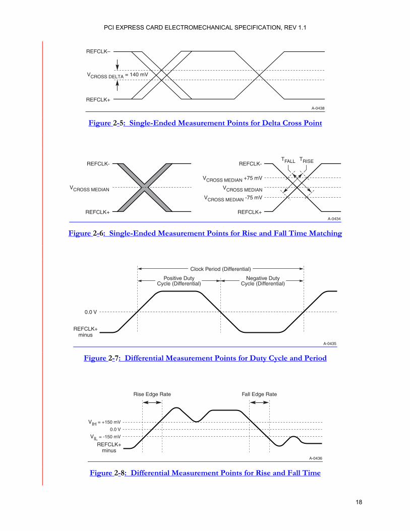
REFCLK–
A-0438
REFCLK+
VCROSS DELTA = 140 mV
Figure 2-5: Single-Ended Measurement Points for Delta Cross Point
A-0434
REFCLK-
REFCLK+
REFCLK-
REFCLK+
VCROSS MEDIAN
VCROSS MEDIAN +75 mV
VCROSS MEDIAN -75 mV
VCROSS MEDIAN
TRISETFALL
Figure 2-6: Single-Ended Measurement Points for Rise and Fall Time Matching
A-0435
REFCLK+minus
0.0 V
Clock Period (Differential)
Positive DutyCycle (Differential)
Negative DutyCycle (Differential)
Figure 2-7: Differential Measurement Points for Duty Cycle and Period
A-0436
Rise Edge Rate Fall Edge Rate
REFCLK+minus
VIH = +150 mV
VIL = -150 mV
0.0 V
Figure 2-8: Differential Measurement Points for Rise and Fall Time

PCI EXPRESS CARD ELECTROMECHANICAL SPECIFICATION, REV 1.1
19
A-0432
TSTABLE
TSTABLE
VRB
VRB
REFCLK+minus
VIH = +150 mV
VIL = -150 mV
0.0 VVRB = +100 mV
VRB = -100 mV
Figure 2-9: Differential Measurement Points for Ringback
A-0433
ReferenceClock
Rs
Rs MotherboardTrace
ZC-DCZC-DC
PCI ExpressConnector
1.0" Add-In
PCI Express Add-InCard Test
REFCLK+
REFCLK-
CL = 2 pF CL = 2 pF
Figure 2-10: Reference Clock System Measurement Point and Loading
PCI EXPRESS CARD ELECTROMECHANICAL SPECIFICATION, REV 1.1
20
2.1.4. REFCLK Phase Jitter Specification
The phase jitter of the reference clock is to be measured using the following clock recovery function
[ ] )(*)()()( 3_*
21 sHesHsHsH delayts ⋅−= −
where 5
211
2
211
1 22
)(ωζω
ωζω++
+=
sss
sH ,
222
2
222
2 22
)(ωζω
ωζω++
+=
sss
sH ,
33 )(
ω+=
sssH ,
( )
( )
sdelayt
sRad
sRad
sRad
9
63
222
6
2
222
6
1
1010_
/105.1**2
/12121
105.1**2
/12121
1022**254.0
−⋅=
⋅=
++++
⋅=
++++
⋅=
=
πω
ζζ
πω
ζζ
πω
ζ
10
The maximum allowed magnitude of the peak-peak reference clock jitter is given inTable 2-2. For information about the maximum peak-peak phase jitter value refer to PCI Express Jitter Modeling. Multiple methods can be used to measure the maximum allowed peak-peak phase jitter value. Real time sampling scopes must use a sampling rate of 20 giga-samples per second or better and take enough data to guarantee the proper bit error rate (BER). Reference clock measurements for cards 15 should be taken with a differential, high-impedance probe using the circuit of Figure 2-10 at the load capacitors CL. Measurements for devices on the same board should be made using a differential, high-impedance probe as close to the REFCLK+ and REFCLK- input pins as possible.
Table 2-2: Maximum Allowed Phase Jitter When Applied to Fixed Filter Characteristic
BER Maximum Peak-Peak Phase Jitter Value (ps)
10-6 86
10-12 108
PCI EXPRESS CARD ELECTROMECHANICAL SPECIFICATION, REV 1.1
21
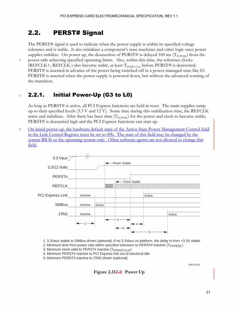
2.2. PERST# Signal The PERST# signal is used to indicate when the power supply is within its specified voltage tolerance and is stable. It also initializes a component’s state machines and other logic once power supplies stabilize. On power up, the deassertion of PERST# is delayed 100 ms (TPVPERL) from the power rails achieving specified operating limits. Also, within this time, the reference clocks 5 (REFCLK+, REFCLK-) also become stable, at least TPERST-CLK before PERST# is deasserted. PERST# is asserted in advance of the power being switched off in a power-managed state like S3. PERST# is asserted when the power supply is powered down, but without the advanced warning of the transition.
2.2.1. Initial Power-Up (G3 to L0) 10
As long as PERST# is active, all PCI Express functions are held in reset. The main supplies ramp up to their specified levels (3.3 V and 12 V). Some time during this stabilization time, the REFCLK starts and stabilizes. After there has been time (TPVPERL) for the power and clock to become stable, PERST# is deasserted high and the PCI Express functions can start up.
On initial power-up, the hardware default state of the Active State Power Management Control field 15 in the Link Control Register must be set to 00b. The state of this field may be changed by the system BIOS or the operating system only. Other software agents are not allowed to change this field.
OM14742A
5
4
3.3 Vaux
3.3/12 Volts
PERST#
REFCLK
PCI Express Link
SMBus
JTAG
Inactive
Inactive
Inactive
Active
Active
Active
Clock Stable
Power Stable
3
21
1. 3.3Vaux stable to SMBus driven (optional). If no 3.3Vaux on platform, the delay is from +3.3V stable2. Minimum time from power rails within specified tolerance to PERST# inactive (TPVPERL)3. Minimum clock valid to PERST# inactive (TPERST-CLK)4. Minimum PERST# inactive to PCI Express link out of electrical idle5. Minimum PERST# inactive to JTAG driven (optional)
Figure 2-112-2: Power Up

PCI EXPRESS CARD ELECTROMECHANICAL SPECIFICATION, REV 1.1
22
2.2.2. Power Management States (S0 to S3/S4 to S0)
If the system wants to enter S3/S4, devices are placed into D3hot states with Links in L2 prior to any power transitions at the slot. The main power and reference clock supplied to the PCI Express slot will go inactive and stay inactive until a wakeup event. As a result of the removal of main power, devices enter the D3cold state. During the D3cold state, +3.3Vaux remains at 3.3 V. On the wakeup 5 event, the power manager restores the main power and reference clocks. As in the last section, PERST# deasserts TPVPERL after the clocks and power are stable.
On resume from a D3cold state, the hardware default state of the Active State Power Management Control field in the Link Control Register must be set to 00b. The state of this field may be changed by the system BIOS or the operating system only. Other software agents are not allowed to change 10 this field.
OM14743A
1. The PCI Express link will be put into electrical idle prior to PERST# going active.2. PERST# goes active before the power on the connector is removed.3. Clock and JTAG go inactive after PERST# goes active.4. A wakeup event resumes the power to the connector, restarts the clock, and the sequence proceeds as in power up.5. The minimum active time for PERST# is TPERST.
5
4
3.3 Vaux
3.3/12 Volts
PERST#
REFCLK
PCI Express Link
SMBus
JTAG
Inactive
ActiveActive
Active
Active
Active
Inactive Active
Active
Active
Clock Stable
Power Stable
Clock not Stable
Power StableWakeup Event
3
2
1
Figure 2-132-3: Power Management States
2.2.3. Power Down
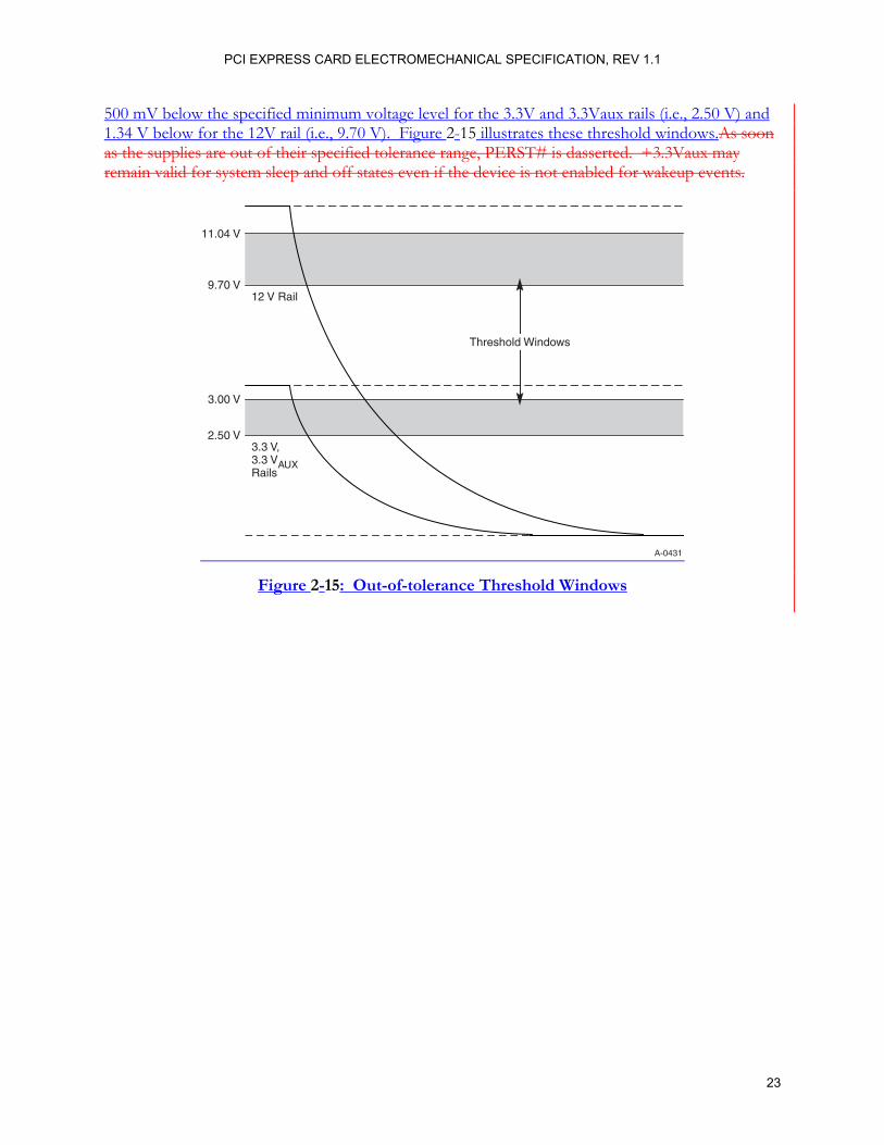
A power rail (12V, 3.3V, or 3.3Vaux) is deemed to be valid or stable if the specified voltage is within the associated voltage tolerances defined in Table 4-1. Once a power rail is deemed stable, an invalid or unstable rail is defined as a rail that has dropped below the specified minimum voltage 15 levels (e.g., below 3.00 V for the 3.3V rails). For purposes of detecting an out-of-tolerance power source, the threshold for detection should be established in a window range of no more than
PCI EXPRESS CARD ELECTROMECHANICAL SPECIFICATION, REV 1.1
23
500 mV below the specified minimum voltage level for the 3.3V and 3.3Vaux rails (i.e., 2.50 V) and 1.34 V below for the 12V rail (i.e., 9.70 V). Figure 2-15 illustrates these threshold windows.As soon as the supplies are out of their specified tolerance range, PERST# is dasserted. +3.3Vaux may remain valid for system sleep and off states even if the device is not enabled for wakeup events.
A-0431
11.04 V
9.70 V
3.00 V
2.50 V
12 V Rail
3.3 V,3.3 VAUXRails
Threshold Windows
Figure 2-15: Out-of-tolerance Threshold Windows
PCI EXPRESS CARD ELECTROMECHANICAL SPECIFICATION, REV 1.1
24
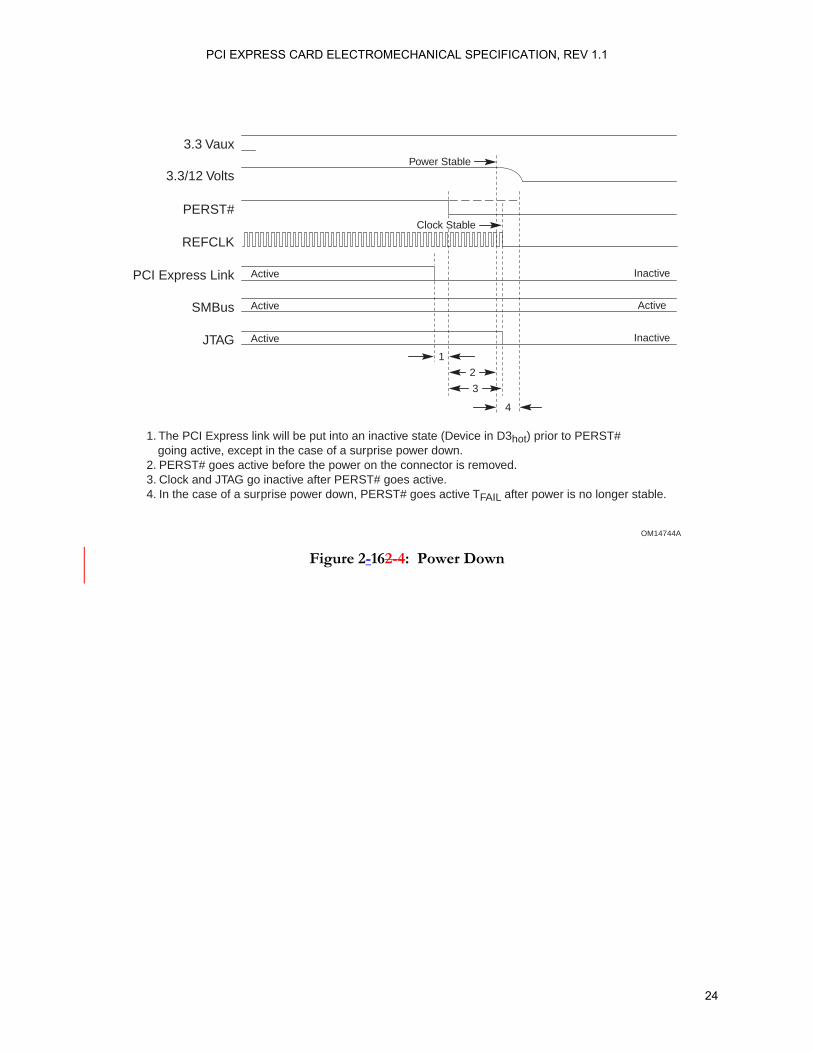
OM14744A
1. The PCI Express link will be put into an inactive state (Device in D3hot) prior to PERST# going active, except in the case of a surprise power down.2. PERST# goes active before the power on the connector is removed.3. Clock and JTAG go inactive after PERST# goes active.4. In the case of a surprise power down, PERST# goes active TFAIL after power is no longer stable.
4
3.3 Vaux
3.3/12 Volts
PERST#
REFCLK
PCI Express Link
SMBus
JTAG
Active
Active
Active
Inactive
Active
Inactive
Clock Stable
Power Stable
2
3
1
Figure 2-162-4: Power Down
PCI EXPRESS CARD ELECTROMECHANICAL SPECIFICATION, REV 1.1
25
2.3. WAKE# Signal The WAKE# signal is an open drain, active low signal that is driven low by a PCI Express component to reactivate the PCI Express slot’s main power rails and reference clocks. Only add-in cards that support the wake process connect to this pin. If the add-in card has wakeup capabilities, it must support the WAKE# function. Likewise, only systems that support the wakeup function 5 need to connect to this pin, but if they do, they must fully support the WAKE# function. Such systems are not required to support Beacon as a wakeup mechanism, but are encouraged to support it. If the wakeup process is used, the +3.3Vaux supply must be present and used for this function. The assertion and de-assertion of WAKE# are asynchronous to any system clock. (See Chapter 5 of the PCI Express Base Specification, Revision 1.1 for more details on PCI-compatible power 10 management.)
If the WAKE# signal is supported by a slot, the signal is connected to the platform’s power management (PM) controller. WAKE# may be bused to all PCI Express add-in card connectors, forming a single input connection at the PM controller or individual connectors can have individual connections to the PM controller. Hot-Plug requires that WAKE# be isolated between connectors 15 and driven inactive during the Hot-Plug/Hot Removal events. Refer to Section 5.15.1 for the connector pin assignment for the WAKE# signal.
Auxiliary power (+3.3Vaux) must be used by the asserting and receiving ends of WAKE# in order to revive the hierarchy. The system vendor must also provide a pull-up on WAKE# with its bias voltage reference being supplied by the auxiliary power source in support of Link reactivation. Note 20 that the voltage that the system board uses to terminate the WAKE# signal can be lower than the auxiliary supply voltage to be compatible with lower voltage processes of the system PM controller. However, all potential drivers of the WAKE# signal must be 3.3 V tolerant.
Note: WAKE# is not PME# and should not be attached to the PCI-PME# interrupt signals. WAKE# causes power to be restored but must not directly cause an interrupt. 25
WAKE# has additional electrical requirements over and above standard open drain signals that allow it to be shared between devices that are powered off and those that are powered on using auxiliary power for example. The additional requirements include careful circuit design to ensure that a voltage applied to the WAKE# signal network never causes damage to a component even if that particular component’s power is not applied. 30
Additionally, the device must ensure that it does not pull WAKE# low unless WAKE# is being intentionally asserted in all cases, including when the related function is in D3cold.
This means that any component implementing WAKE# must be designed such that:
Unpowered WAKE# output circuits are not damaged if a voltage is applied to them from other powered “wire-ORed” sources of WAKE#. 35
When power is removed from its WAKE# generation logic, the unpowered output does not present a low impedance path to ground or any other voltage.
These additional requirements ensure that the WAKE# signal network continues to function properly when a mixture of auxiliary powered, and unpowered components have their WAKE# outputs wire-ORed together. It is important to note that most commonly available open drain, and 40
PCI EXPRESS CARD ELECTROMECHANICAL SPECIFICATION, REV 1.1
26
tri-state buffer circuit designs used “as is” do not satisfy the additional circuit design requirements for WAKE#.
Other requirements on the system board/add-in card designer include:
Common ground plane reference between slots/components attached to the same WAKE# signal. 5
Split voltage power planes (+3.3Vaux vs. +3.3V) are required if +3.3Vaux is supplied to the connector(s).
If +3.3Vaux is supplied to one PCI Express connector in a chassis, it must be supplied to all PCI Express connectors in that chassis.
If WAKE# is supported on one PCI Express connector in a chassis, it must be supported on all 10 PCI Express connectors in that chassis.
If the system does not support +3.3Vaux or the wakeup function, the +3.3Vaux connector pin is left open on the system board. See the PCI Bus Power Management Interface Specification, Revision. 1.1 2 for +3.3Vaux power requirements.
+3.3Vaux voltage supply may be present even if the device is not enabled for wakeup events. 15
+3.3V at the PCI Express connector may be switched off by the system.
Add-in cards are permitted to generate the Beacon wakeup mechanism in addition to using the WAKE# mechanism, although the system is not required to provide support for Beacon.
Note: If the add-in card uses the Beacon mechanism in addition to the WAKE# mechanism, the Beacon may be ignored by the system. Circuits that support the wake function and are intended 20 to work in any PCI Express system must be designed to generate the Beacon on their PCI Express data lines.
PCI Express add-in card designers must be aware of the special requirements that constrain WAKE# and ensure that their add-in cards do not interfere with the proper operation of the WAKE# network. The WAKE# input into the system may de-assert as late as 100 ns after the 25 WAKE# output from the function de-asserts (i.e., the WAKE# pin must be considered indeterminate for a number of cycles after it has been de-asserted).
The value of the pull-up resistor for WAKE# on the system board must be derived taking into account the total possible capacitance on WAKE# to ensure that WAKE# charges up to a logic high voltage level in no more than 100 ns. (See Section 4.3.3 of the PCI Local Bus Specification, 30 Revision 3.0 for information on pull-up resistors.)

PCI EXPRESS CARD ELECTROMECHANICAL SPECIFICATION, REV 1.1
27
IMPLEMENTATION NOTE Example WAKE# Circuit Design The following diagram is an example of how the WAKE# generation logic could be implemented. In this example, multiple PCI Express functions have their WAKE# signals ganged together and connected to the single WAKE# pin on the PCI Express add-in card connector. 5
The circuit driving the gate of transistor Q1 is designed to isolate the add-in card’s WAKE# network from that of the system board whenever its power source (VSOURCE) is absent.
If the card supplies power to its WAKE# logic with the PCI Express connector’s 3.3 V supply (i.e., it does not support wakeup from D3cold), then all WAKE# sources from the card will be isolated from the system board when the add-in card’s +3.3V rail is switched off. Add-in cards that support 10 wakeup from D3cold have an auxiliary power source (+3.3Vaux) to power the WAKE# logic which maintains connection of these WAKE# sources to the system board’s WAKE# signal network even when the Link hierarchy’s power (+3.3V) has been switched off.
OM14749
Card–Wake (0)#
Card–Wake (1)#
Card–Wake (n)#
U1
U1
U1
Q1U2
R2
R1
R3
DG
S Wake #
+
–
3.3Vaux
Q2
VSOURCE+–
System BoardAdd-in Card
Q1 = FETQ2 = Zener DiodeU1 = Open Drain BufferU2 = ComparatorVSOURCE = Voltage source for Wake# logic (either PCI Express connector Vcc
or an auxiliary voltage source)
3.3Vaux = Auxiliary voltage source provided by the system's
power supply
This example assumes that all sources of WAKE# on the add-in card are powered by either the +3.3V or +3.3Vaux (VSOURCE). If WAKE# from D3cold is supported by some, but not all of the add-15

PCI EXPRESS CARD ELECTROMECHANICAL SPECIFICATION, REV 1.1
28
in card’s functions that generate WAKE#, the add-in card designer must ensure that there is separate isolation control for each of the WAKE# generation power sources.
PCI Express component designers could choose to integrate the “power fail detect” isolation circuitry with their WAKE# output pin physically corresponding to the source of FET Q1. Alternatively, all isolation control logic could be implemented externally on the add-in card. 5
This example is meant as a conceptual aid, and is not intended to prescribe an actual implementation.
2.4. SMBus (Optional) The optional System Management Bus (SMBus) is a two-wire interface through which various system component chips can communicate with each other and with the rest of the system. It is 10 based on the principles of operation of I2C.
SMBus provides a control bus for system and power management related tasks. A system may use SMBus to pass messages to and from devices instead of tripping individual control lines. Removing the individual control lines reduces pin count. Accepting messages ensures future expandability.
With SMBus, a device can provide manufacturer information, tell the system what its model/part 15 number is, save its state for a suspend event, report different types of errors, accept control parameters, and return its status.
SMBus is described in System Management Bus (SMBus) Specification, Version 2.0. Refer to this specification for DC characteristics and all AC timings. If the system board or add-in card supports SMBus, it must adhere to additional requirements that may be found in Chapter 8 of the PCI Local 20 Bus Specification, Revision. 2.33.0.
The system board provides pull-ups to the +3.3Vaux rail per the above specification and the components attached to these signals need to have a 3.3 V signaling tolerance.
2.4.1. Capacitive Load of High-power SMBus Lines
Capacitive load for each bus line includes all pin, wire, and connector capacitances. The maximum 25 capacitive load affects the selection of the pull-up resistor or the current source in order to meet the rise time specifications of SMBus.
Normally, pin capacitance is defined as the total capacitive load of one SMBus device as seen in a typical manufacturer’s data sheet. The value in the DC specifications (COUT in Table 2-3) is a recommended guideline so that two SMBus devices may, for example, be populated on an add-in 30 card.
PCI EXPRESS CARD ELECTROMECHANICAL SPECIFICATION, REV 1.1
29
2.4.2. Minimum Current Sinking Requirements for SMBus Devices
While SMBus devices used in low-power segments have practically no minimum current sinking requirements due to the low pull-up current specified for low-power segments, devices in high-power segments are required to sink a minimum current of 4 mA while maintaining the VOL(max) of 5 0.4 V. The requirement for 4 mA sink current determines the minimum value of the pull-up resistor RP that can be used in SMBus systems.
2.4.3. SMBus “Back Powering” Considerations
Unpowered devices connected to either a low-power or high-power SMBus segment must provide, either within the device or through the interface circuitry, protection against “back powering” the 10 SMBus. Unpowered devices connected to high-power segments must meet leakage specifications in Section 3.1.2.1 of the System Management Bus (SMBus) Specification, Version 2.0.
2.4.4. Power-on Reset
SMBus devices detect a power-on event in one of three ways:
By detecting that power is being applied to the device 15
By PERST# being asserted
For self-powered or always powered devices, by detecting that the SMBus is active (clock and data lines have gone high after being low for more than 2.5 s)
An SMBus device must respond to a power-on event by bringing the device into an operational state within tPOR, defined in Table 1 of the System Management Bus (SMBus) Specification, Version 2.0, after the 20 device has been supplied power that is within the device’s normal operating range. Self-powered or always-powered devices, such as Smart Batteries, are not required to do a complete power-on reset but they must be in an operational state within 500 ms after the SMBus becomes active.
PCI EXPRESS CARD ELECTROMECHANICAL SPECIFICATION, REV 1.1
30
2.5. JTAG Pins (Optional) The IEEE Standard 1149.1, Test Access Port and Boundary Scan Architecture, is included as an optional interface for PCI Express devices. IEEE Standard 1149.1 specifies the rules and permissions for designing an 1149.1-compliant interface. Inclusion of a Test Access Port (TAP) on an add-in card allows boundary scan to be used for testing of the card on which it is installed. The TAP is 5 comprised of four pins (optionally five) that are used to interface serially with a TAP controller within the PCI Express device.
TCK in Test Clock is used to clock state information and test data into and out of the device during operation of the TAP.
TDI in Test Data Input is used to serially shift test data and test 10 instructions into the device during TAP operation.
TDO out Test Output is used to serially shift test data and test instructions out of the device during TAP operation.
TMS in Test Mode Select is used to control the state of the TAP controller in the device. 15
TRST# in Test Reset provides an asynchronous initialization of the TAP controller. This signal is optional in IEEE Standard 1149.1. These TAP pins operate at 3.3V, the same as the other single-ended I/O signals of the PCI Express connector. The drive strength of the TDO pin is not required to be the same as other PCI Express 20 pins. The add-in card vendor must specify TDO drive strength. The direction of these TAP pins is defined from the perspective of the add-in card.
The system vendor is responsible for the design and operation of the 1149.1 serial chains (“rings”) required in the system. The signals are supplementary to the PCI Express interface. Additional information can be found in the PCI Local Bus Specification, Revision. 2.33.0, Section 2.2.9. 25
PCI EXPRESS CARD ELECTROMECHANICAL SPECIFICATION, REV 1.1
31
2.6. Auxiliary Signal Parametric Specifications
2.6.1. DC Specifications
Table 2-32-1: Auxiliary Signal DC Specifications - PERST#, WAKE#, and SMBus
Symbol Parameter Conditions Min Max Unit Notes
VIL1 Input Low Voltage
-0.5 0.8 V 2
VIH1 Input High Voltage
2.0 Vcc3_3 + 0.5 V 2
VIL2 Input Low Voltage
-0.5 0.8 V 4
VIH2 Input High Voltage
2.1 VccSus3_3 + 0.5 V 4
VOL1 Output Low Voltage 4.0 mA 0.2 V 1, 3
VHMAX Max High Voltage Vcc3_3 + 0.5 V 3
VOL2 Output Low Voltage 4.0 mA 0.4 V 1, 4
Iin Input Leakage Current 0 to 3.3 V -10 +10 µA 2, 4
Ilkg Output Leakage Current 0 to 3.3 V -50 +50 µA 3, 4, 5
Cin Input Pin Capacitance 7 pF 2
Cout Output (I/O) Pin Capacitance 30 pF 3,4
Notes: 1. Open-drain output a pull-up is required on the system board. There is no VOH specification for
these signals. The number given is the maximum voltage that can be applied to this pin. 5 2. Applies to PERST#. 3. Applies to WAKE#. 4. Applies to SMBus signals SMBDATA and SMBCLK. 5. Leakage at the pin when the output is not active (high impedance).
PCI EXPRESS CARD ELECTROMECHANICAL SPECIFICATION, REV 1.1
32
2.6.2. AC Specifications
Table 2-52-2: Power Sequencing and Reset Signal Timings
Symbol Parameter Min Max Units Notes Figure
TPVPERL Power stable to PERST# inactive 100 ms 1 Figure 2-11
TPERST-CLK REFCLK stable before PERST# inactive 100 µs 2 Figure 2-11
TPERST PERST# active time 100 µs Figure 2-13
TFAIL Power level invalid to PERST#PWRGD inactive 500 ns 3 Figure 2-16
TWKRF WAKE# rise – fall time 100 ns 4 Figure 2-18
Notes: 1. Any supplied power is stable when it meets the requirements specified for that power supply. 2. A supplied reference clock is stable when it meets the requirements specified for the reference clock. The
PERST# signal is asserted and de-asserted asynchronously with respect to the supplied reference clock. 5 3. The PERST# signal must be asserted within TFAIL of any supplied power going out of specification. 4. Measured from WAKE# assertion/de-assertion to valid input level at the system PM controller. Since WAKE# is
an open-drain signal, the rise time is dependent on the total capacitance on the platform and the system board pull-up resistor. It is the responsibility of the system designer to meet the rise time specification.
A-0338
Wake#
VIH_PMC1
VIL_PMC1
Wake#
TWKRF
Note 1: Power Management Controller input switching levels are platform dependent and are not set by this specification.
Figure 2-182-5: WAKE# Rise and Fall Time Measurement Points
PCI EXPRESS CARD ELECTROMECHANICAL SPECIFICATION, REV 1.1
33
2.6.3.REFCLK Specifications

PCI EXPRESS CARD ELECTROMECHANICAL SPECIFICATION, REV 1.1
34
3. Hot Insertion and Removal In the following text, all references to mechanical elements should be interpreted in the context of the PCI Express card form factor definition, unless otherwise stated.
3.1. Scope The PCI Express specification natively supports Hot-Plug/Hot Removal of PCI Express add-in 5 cards. However, hardware support of Hot-Plug/Hot-Removal on the system board is optional. Since the PCI Express evolutionary form factor is designed as a direct PCI connector replacement and utilizes an edge card connector, the PCI Express Native Hot-Plug model is based on the standard usage model defined in the PCI Standard Hot-Plug Controller and Subsystem Specification, Revision 1.0. 10
The following section describes the add-in card presence detect and PCI Express Native Hot-Plug signals. For a detailed explanation of the register requirements and standard usage model, see Chapter 7 of the PCI Express Base Specification, Revision 1.1.
3.2. Presence Detect The PCI Express Hot-Plug controller detects the presence of an add-in card using the PRSNT2# 15 signal as shown in Figure 3-1. It is the responsibility of the Root Complex or the switch to determine the presence of the add-in card and set the present bits in the appropriate register as described in Chapter 7 of the PCI Express Base Specification, Revision 1.1. In addition to the Hot-Plug controller, the PRSNT2# signal is used by the system board to recognize the presence of the add-in card in order to enable the auxiliary signals: CLK, PERST#, SMBus, and JTAG. The two signals, 20 PRSNT1# and PRSNT2#, described in Figure 3-1, are required on the PCI Express connector and must be supported by all PCI Express add-in cards.
Both PRSNT1# and PRSNT2# signals are required in order to detect the presence of the add-in card and to ensure that it is fully inserted in the connector.Figure 3-1 shows the presence detection mechanism. Both of these pins are required in order to detect the presence of the add-in card and 25 to ensure that it is fully inserted in the connector. Note that the pads on the add-in card for the PRSNT1# and PRSNT2# signals are shorter than the rest of the pads in order to have about 1 ms difference of insertion time. Unused PRSNT2# pads on x4, x8, and x16 add-in cards can be either standard length or the pad can be eliminated. This scheme is used to allow the power switches to isolate the power to the card during surprise removal. The mechanical details are provided in 30 Chapter 5.
3
PCI EXPRESS CARD ELECTROMECHANICAL SPECIFICATION, REV 1.1
35
Gold Fingers
OM14750A
PCI Express Add-in Card
PRSNT1# PRSNT2# Hot PlugControl Logic
PULL-UPMate Last /Break First
System Board
SystemBoard
Connector
Trace on the Add-in Card[actual trace routing is left up to the board designer]
45˚
PRSNT1# PRSNT2#
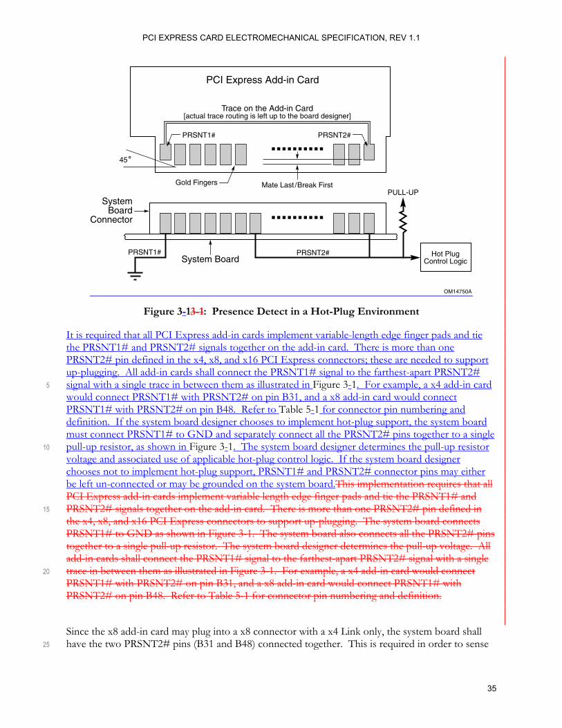
Figure 3-13-1: Presence Detect in a Hot-Plug Environment
It is required that all PCI Express add-in cards implement variable-length edge finger pads and tie the PRSNT1# and PRSNT2# signals together on the add-in card. There is more than one PRSNT2# pin defined in the x4, x8, and x16 PCI Express connectors; these are needed to support up-plugging. All add-in cards shall connect the PRSNT1# signal to the farthest-apart PRSNT2# signal with a single trace in between them as illustrated in Figure 3-1. For example, a x4 add-in card 5 would connect PRSNT1# with PRSNT2# on pin B31, and a x8 add-in card would connect PRSNT1# with PRSNT2# on pin B48. Refer to Table 5-1 for connector pin numbering and definition. If the system board designer chooses to implement hot-plug support, the system board must connect PRSNT1# to GND and separately connect all the PRSNT2# pins together to a single pull-up resistor, as shown in Figure 3-1. The system board designer determines the pull-up resistor 10 voltage and associated use of applicable hot-plug control logic. If the system board designer chooses not to implement hot-plug support, PRSNT1# and PRSNT2# connector pins may either be left un-connected or may be grounded on the system board.This implementation requires that all PCI Express add-in cards implement variable length edge finger pads and tie the PRSNT1# and PRSNT2# signals together on the add-in card. There is more than one PRSNT2# pin defined in 15 the x4, x8, and x16 PCI Express connectors to support up-plugging. The system board connects PRSNT1# to GND as shown in Figure 3-1. The system board also connects all the PRSNT2# pins together to a single pull-up resistor. The system board designer determines the pull-up voltage. All add-in cards shall connect the PRSNT1# signal to the farthest-apart PRSNT2# signal with a single trace in between them as illustrated in Figure 3-1. For example, a x4 add-in card would connect 20 PRSNT1# with PRSNT2# on pin B31, and a x8 add-in card would connect PRSNT1# with PRSNT2# on pin B48. Refer to Table 5-1 for connector pin numbering and definition.
Since the x8 add-in card may plug into a x8 connector with a x4 Link only, the system board shall have the two PRSNT2# pins (B31 and B48) connected together. This is required in order to sense 25

PCI EXPRESS CARD ELECTROMECHANICAL SPECIFICATION, REV 1.1
36
the presence of the x8 add-in card in a x8 connector that supports a x4 Link only. See Section 6.3 for card interoperability discussions.

PCI EXPRESS CARD ELECTROMECHANICAL SPECIFICATION, REV 1.1
37

PCI EXPRESS CARD ELECTROMECHANICAL SPECIFICATION, REV 1.1
38
4. Add-in Card Electrical Requirements Power delivery requirements defined in this chapter apply not only to add-in cards, but also to connectors and systems.
4.1. Power Supply Requirements All PCI Express add-in card connectors require two power rails: +12V and +3.3V, with a third, 5 optional 3.3Vaux rail. Systems that provide PCI Express add-in card connectors are required to provide both the +12V and +3.3V rails to every PCI Express add-in card connector in the system. The 3.3Vaux rail may be supplied to the PCI Express add-in card connectors at the system board designers’ discretion. However, if a system board designer does supply 3.3Vaux to the PCI Express add-in card connector, the 3.3Vaux rail must be supplied to all PCI Express add-in card connectors. 10 In addition, as described in Chapter 2, if the platform with the PCI Express interface supports the WAKE# signal, the 3.3Vaux rail (as well as the WAKE# signal) must be supplied to all PCI Express add-in card connectors.
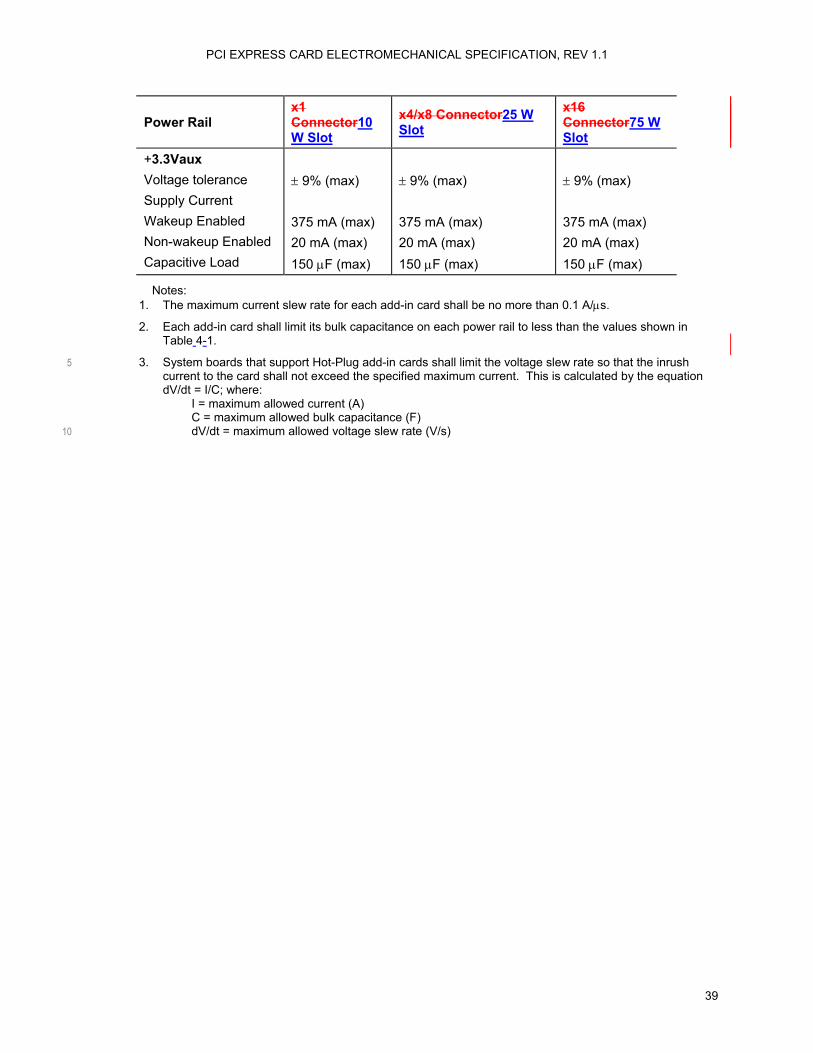
Table 4-1 provides the required specifications for the power supply rails available at the PCI Express connectors, based on the number of PCI Express lanes supported by the connectorsslots. The 15 system designer is responsible for ensuring that the power delivered to the PCI Express connectors meets the specifications called out in Table 4-1.
Table 4-14-1: Power Supply Rail Requirements
Power Rail x1 Connector10 W Slot
x4/x8 Connector25 W Slot
x16 Connector75 W Slot
+3.3V Voltage tolerance Supply Current Capacitive Load
± 9% (max) 3.0 A (max) 1000 µF (max)
± 9% (max) 3.0 A (max) 1000 µF (max)
± 9% (max) 3.0 A (max) 1000 µF (max)
+12V Voltage tolerance Supply Current Capacitive Load
± 8% 0.5 A 300 µF (max)
± 8% 2.1 A (max) 1000 µF (max)
± 8% 4.45.5 A (max) 2000 µF (max)
4
PCI EXPRESS CARD ELECTROMECHANICAL SPECIFICATION, REV 1.1
39
Power Rail x1 Connector10 W Slot
x4/x8 Connector25 W Slot
x16 Connector75 W Slot
+3.3Vaux Voltage tolerance Supply Current Wakeup Enabled Non-wakeup Enabled Capacitive Load
± 9% (max) 375 mA (max) 20 mA (max) 150 µF (max)
± 9% (max) 375 mA (max) 20 mA (max) 150 µF (max)
± 9% (max) 375 mA (max) 20 mA (max) 150 µF (max)
Notes: 1. The maximum current slew rate for each add-in card shall be no more than 0.1 A/µs.
2. Each add-in card shall limit its bulk capacitance on each power rail to less than the values shown in Table 4-1.
3. System boards that support Hot-Plug add-in cards shall limit the voltage slew rate so that the inrush 5 current to the card shall not exceed the specified maximum current. This is calculated by the equation dV/dt = I/C; where: I = maximum allowed current (A) C = maximum allowed bulk capacitance (F) dV/dt = maximum allowed voltage slew rate (V/s) 10

PCI EXPRESS CARD ELECTROMECHANICAL SPECIFICATION, REV 1.1
40
4.2. Power Consumption This specification provides various sizes of cards for system implementation. Each card size provides support for a certain number of PCI Express lanes, and a corresponding difference in specified power consumption as shown in Table 4-3.
Table 4-34-2: Add-in Card Power Dissipation
X1 x4/x8 x16 Standard height 10 W1
(max) 25 W1 (max)
25 W (max) 25 W2 (max)
7560 W2, 4 (max)
Low profile card3 10 W (max) 10 25 W (max) 25 W (max)
Notes: 5 1. A standard height x1 add-in card intended for desktop applications is limited in length to
a half-length add-in card and 10 W maximum power dissipation. A standard height x1 add-in card intended for server I/O applications with 25 W maximum power dissipation must be greater than or equal to 177.80 mm (7.0 inches) in length, but must not exceed a full-length add-in card. See Table 6-1 for add-in card size definitions. The same server 10 I/O add-in card must, at initial power-up, not exceed 10 W of power dissipation, until configured as a high power device, at which time it must not exceed 25 W of power dissipation. Refer to Chapter 6 of the PCI Express Base Specification, Revision 1.1 for information on the power configuration mechanism.
2. A standard height x16 add-in card intended for server I/O applications must limit its 15 power dissipation to 25 W. A standard height x16 add-in card intended for graphics applications must, at initial power-up, not exceed 25 W of power dissipation, until configured as a high power device, at which time it must not exceed 60 75 W of power dissipation. Refer to Chapter 6 of the PCI Express Base Specification Specification, Revision 1.1 for information on the power configuration mechanism. 20
3. All low profile add-in cards are limited in length to a half-length add-in card and must not exceed the power dissipation values shown in Table 4-3.
4. A x16 graphics card is limited to 7560 W. The 7560 W maximum can be drawn via the combination of +12V and +3.3V rails, but each rail draw is limited as defined in Table 4-1, and the sum of the draw on the two rails cannot exceed 7560 W. 25
The power limits for respective connector widths, x1, x4/x8, and x16, represent the add-in card and system capacity to provide cooling for the slot. The 10 W limit assumes natural convection cooling in a system that provides air exchanges. The 25 W and above add-in card power limits assume that sufficient cooling is provided to the slot by the cards in the present chassis environment. In general, the power limits above assume a chassis environment with a maximum internal temperature of 30 55 ºC on the primary component side of the add-in card and natural convection cooling in a system that provides air exchanges. Implementations of other chassis environments should pay special attention to system level thermal requirements.
PCI Express allows for higher maximum power for graphics cards than AGP. In case such a graphics card is used in a system, implementers should pay special attention to system level thermal, 35 acoustic, structure, and power delivery requirements. To insure optimum performance, it is recommended that the system designer refer to the PCI Express Graphics Card Thermal and Mechanical Guideline for Desktop Systems.

PCI EXPRESS CARD ELECTROMECHANICAL SPECIFICATION, REV 1.1
41
IMPLEMENTATION NOTE Software Update of the Slot Power Limit System firmware must update the slot power limit to the system's allocated value for the PCI Express add-in card (e.g., graphics) and ensure the completion of this update prior to invoking the option ROM for that add-in card's PCI Express function. If the initial slot power limit value is set 5 by hardware initialization, then any attempt by software to change that value must be verified by that software prior to initializing the add-in card. Subsequent updates by the system firmware or operating system software, if any, may only increase the slot power limit value. However, after a card is reset, the initial slot power limit value may be lower than the previous value. The maximum power level for an add-in card must be assigned by the system firmware during PCI Express 10 configuration. For graphics, the power level assigned will be dependent on the platform’s support of the PCI Express x16 Graphics 150W-ATX Specification, Revision 1.0 (including the supplemental power cable).
15
4.3. Power Supply Sequencing There is no specific requirement for power supply sequencing of each of the three power supply rails. They may come up or go down in any order. The system, however, must assert the PERST# signal whenever any of the three power rails goes outside of the specifications provided in Table 4-1 (refer to Section 2.2 for specific information on the function and proper use of the PERST# signal). 20
Note: If a PCI Express add-in card requires power supply rail sequencing, it is the responsibility of the add-in card designer to provide appropriate circuitry on the add-in card to meet any power supply rail sequencing requirements.
4.4. Power Supply Decoupling Due to the low level signaling of the PCI Express interface, it is strongly recommended that 25 sufficient decoupling of all power supplies be provided. This is recommended to ensure that power supply noise does not interfere with the recovery of data from a remote upstream PCI Express device. Some basic guidelines to help ensure a quiet power supply are provided below.
Note: The following are guidelines only. It is the responsibility of the add-in card designer to properly test the design to ensure that add-in card circuitry does not create excessive noise on power 30 supply or ground signals at the add-in card edge fingers.
The add-in card device decouple value should average 0.01 µF per device Vcc pin (for all devices on the add-in card).
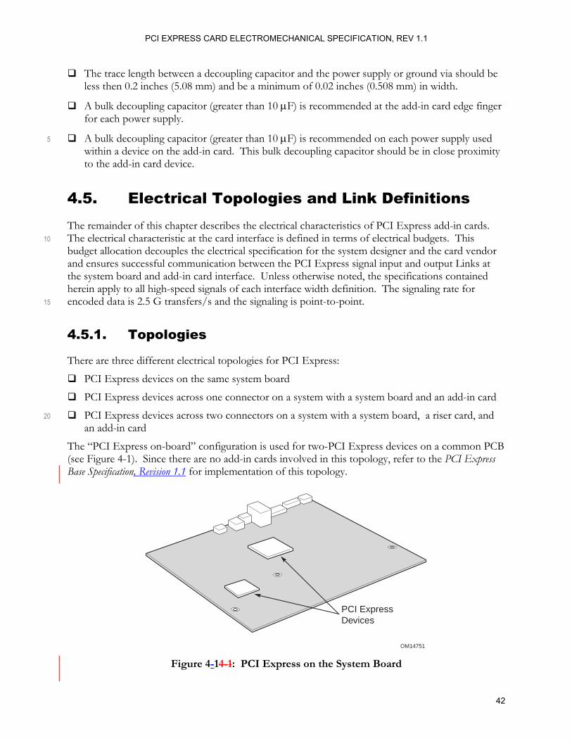
PCI EXPRESS CARD ELECTROMECHANICAL SPECIFICATION, REV 1.1
42
The trace length between a decoupling capacitor and the power supply or ground via should be less then 0.2 inches (5.08 mm) and be a minimum of 0.02 inches (0.508 mm) in width.
A bulk decoupling capacitor (greater than 10 µF) is recommended at the add-in card edge finger for each power supply.
A bulk decoupling capacitor (greater than 10 µF) is recommended on each power supply used 5 within a device on the add-in card. This bulk decoupling capacitor should be in close proximity to the add-in card device.
4.5. Electrical Topologies and Link Definitions The remainder of this chapter describes the electrical characteristics of PCI Express add-in cards. The electrical characteristic at the card interface is defined in terms of electrical budgets. This 10 budget allocation decouples the electrical specification for the system designer and the card vendor and ensures successful communication between the PCI Express signal input and output Links at the system board and add-in card interface. Unless otherwise noted, the specifications contained herein apply to all high-speed signals of each interface width definition. The signaling rate for encoded data is 2.5 G transfers/s and the signaling is point-to-point. 15
4.5.1. Topologies
There are three different electrical topologies for PCI Express:
PCI Express devices on the same system board
PCI Express devices across one connector on a system with a system board and an add-in card
PCI Express devices across two connectors on a system with a system board, a riser card, and 20 an add-in card
The “PCI Express on-board” configuration is used for two-PCI Express devices on a common PCB (see Figure 4-1). Since there are no add-in cards involved in this topology, refer to the PCI Express Base Specification, Revision 1.1 for implementation of this topology.
OM14751
PCI ExpressDevices
Figure 4-14-1: PCI Express on the System Board
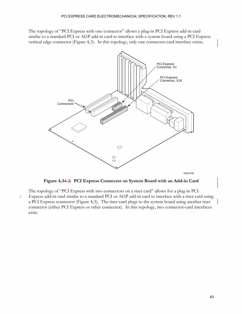
PCI EXPRESS CARD ELECTROMECHANICAL SPECIFICATION, REV 1.1
43
The topology of “PCI Express with one connector” allows a plug-in PCI Express add-in card similar to a standard PCI or AGP add-in card to interface with a system board using a PCI Express vertical edge connector (Figure 4-3). In this topology, only one connector-card interface exists.
PCIConnectors
OM14766
PCI ExpressConnector, X1
PCI ExpressConnector, X16
Figure 4-34-2: PCI Express Connector on System Board with an Add-in Card
The topology of “PCI Express with two connectors on a riser card” allows for a plug-in PCI Express add-in card similar to a standard PCI or AGP add-in card to interface with a riser card using 5 a PCI Express connector (Figure 4-5). The riser card plugs to the system board using another riser connector (either PCI Express or other connector). In this topology, two connector-card interfaces exist.
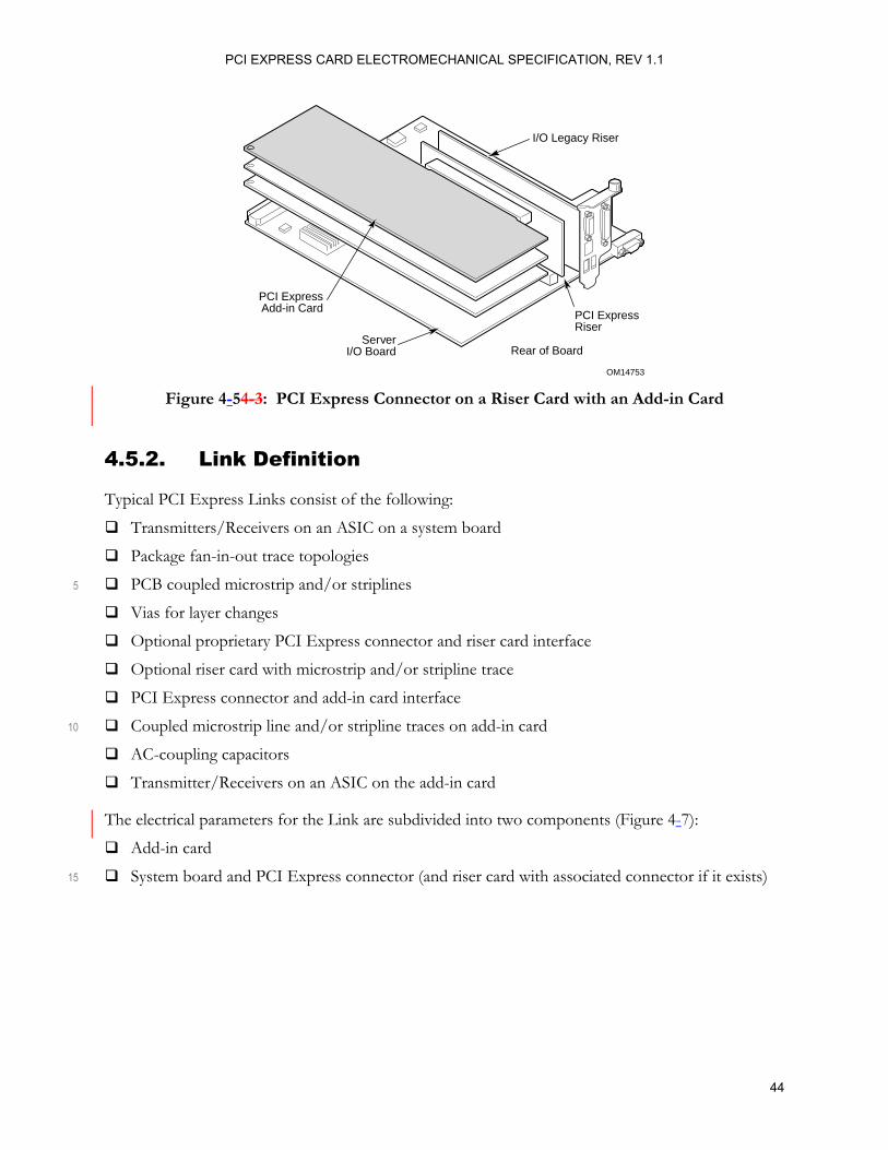
PCI EXPRESS CARD ELECTROMECHANICAL SPECIFICATION, REV 1.1
44
I/O Legacy Riser
PCI ExpressRiser
Rear of BoardServer
I/O Board
PCI ExpressAdd-in Card
OM14753
Figure 4-54-3: PCI Express Connector on a Riser Card with an Add-in Card
4.5.2. Link Definition
Typical PCI Express Links consist of the following:
Transmitters/Receivers on an ASIC on a system board
Package fan-in-out trace topologies
PCB coupled microstrip and/or striplines 5
Vias for layer changes
Optional proprietary PCI Express connector and riser card interface
Optional riser card with microstrip and/or stripline trace
PCI Express connector and add-in card interface
Coupled microstrip line and/or stripline traces on add-in card 10
AC-coupling capacitors
Transmitter/Receivers on an ASIC on the add-in card The electrical parameters for the Link are subdivided into two components (Figure 4-7):
Add-in card
System board and PCI Express connector (and riser card with associated connector if it exists) 15
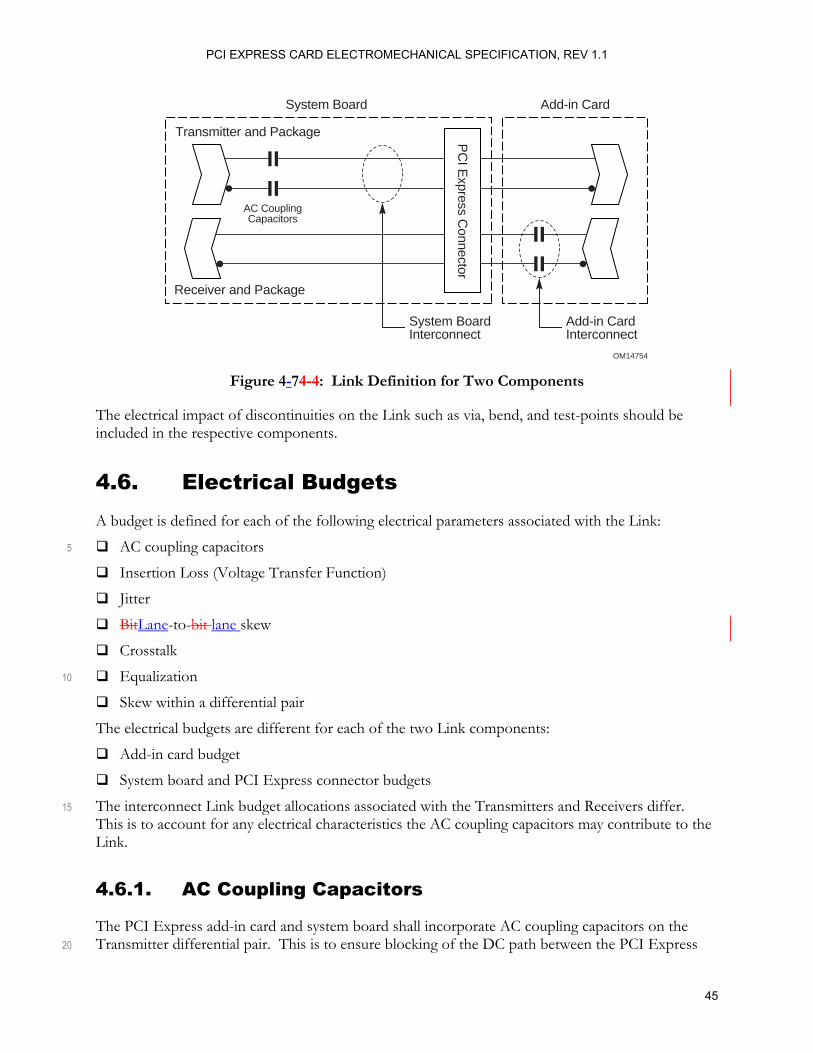
PCI EXPRESS CARD ELECTROMECHANICAL SPECIFICATION, REV 1.1
45
Transmitter and Package
Add-in CardSystem Board
Receiver and Package
PC
I Express C
onnector
Add-in CardInterconnect
System BoardInterconnect
AC CouplingCapacitors
OM14754 Figure 4-74-4: Link Definition for Two Components
The electrical impact of discontinuities on the Link such as via, bend, and test-points should be included in the respective components.
4.6. Electrical Budgets A budget is defined for each of the following electrical parameters associated with the Link:
AC coupling capacitors 5
Insertion Loss (Voltage Transfer Function)
Jitter
BitLane-to-bit lane skew
Crosstalk
Equalization 10
Skew within a differential pair
The electrical budgets are different for each of the two Link components:
Add-in card budget
System board and PCI Express connector budgets
The interconnect Link budget allocations associated with the Transmitters and Receivers differ. 15 This is to account for any electrical characteristics the AC coupling capacitors may contribute to the Link.
4.6.1. AC Coupling Capacitors
The PCI Express add-in card and system board shall incorporate AC coupling capacitors on the Transmitter differential pair. This is to ensure blocking of the DC path between the PCI Express 20
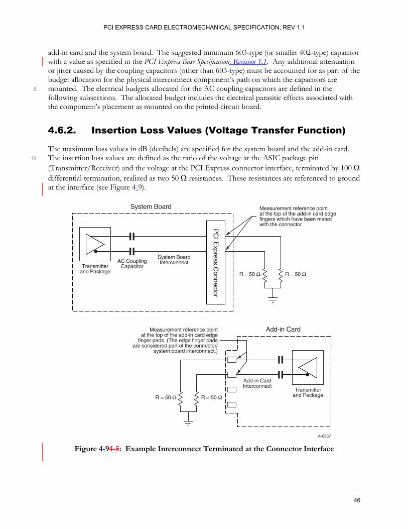
PCI EXPRESS CARD ELECTROMECHANICAL SPECIFICATION, REV 1.1
46
add-in card and the system board. The suggested minimum 603-type (or smaller 402-type) capacitor with a value as specified in the PCI Express Base Specification, Revision 1.1. Any additional attenuation or jitter caused by the coupling capacitors (other than 603-type) must be accounted for as part of the budget allocation for the physical interconnect component’s path on which the capacitors are mounted. The electrical budgets allocated for the AC coupling capacitors are defined in the 5 following subsections. The allocated budget includes the electrical parasitic effects associated with the component’s placement as mounted on the printed circuit board.
4.6.2. Insertion Loss Values (Voltage Transfer Function)
The maximum loss values in dB (decibels) are specified for the system board and the add-in card. The insertion loss values are defined as the ratio of the voltage at the ASIC package pin 10
(Transmitter/Receiver) and the voltage at the PCI Express connector interface, terminated by 100 Ω differential termination, realized as two 50 Ω resistances. These resistances are referenced to ground at the interface (see Figure 4-9).
A-0337
Add-in Card
System Board Measurement reference pointat the top of the add-in card edgefingers which have been matedwith the connector
Transmitterand Package
Transmitterand Package
Add-in CardInterconnect
System BoardInterconnectAC Coupling
Capacitor
R = 50 Ω R = 50 Ω
R = 50 Ω R = 50 Ω
Measurement reference pointat the top of the add-in card edge
finger pads. (The edge finger padsare considered part of the connector/
system board interconnect.)
PC
I Express C
onnector
Figure 4-94-5: Example Interconnect Terminated at the Connector Interface

PCI EXPRESS CARD ELECTROMECHANICAL SPECIFICATION, REV 1.1
47
All PCI Express differential trace pairs are required to be referenced to the ground plane. The loss values associated with any riser card interface and adjoining connector implementation must collectively meet the system board loss budget allocations and associated eye diagrams.
Add-in CardSystem Board
PC
I Express C
onnector
OM14768A
LST LAR
LSR LAT
Figure 4-114-6: Insertion Loss Budgets
Table 4-54-3: Allocation of Interconnect Path Insertion Loss Budget
Loss Parameter
Loss Budget Value at 1.25 GHz (dB)
Loss Budget Value at 625 MHz (dB)
Comments
PCI Express Add-in Card
L AR < 2.65 L AT < 3.84 L AR < 1.95 L AT < 2.94 Notes 1, 2
System Board and Connector
L ST < 9.30 L SR < 8.11 L ST < 65.001 L SR < 56.010 Notes 1, 3
Guard Band 1.25 1.25 Note 1
Total Loss L T < 13.2 L T < 9.2
Notes: 1. All values are referenced to 100 Ω, realized as two 50 Ω resistances. The loss budget 5
values include all possible crosstalk impacts (near-end and far-end) and potential mismatch of the actual interconnect with respect to the 100 Ω reference load.
The PCI Express Base Specification, Revision 1.1 allows an interconnect loss of 13.2 dB for 1.25 GHz (non de-emphasized) signals and 9.2 dB for 625 MHz (de-emphasized) signals. From this, a total of 1.25 dB is held in reserve as guard band to allow for any additional 10 attenuation that might occur when the add-in card and system board are actually mated. The allocated loss budget values in the table directly correlate to the eye diagram voltages in Section 4.7. Tradeoffs in terms of attenuation, crosstalk, and mismatch can be made within the budget allocations specified.
As a guide for design and simulation, the following derivation of the budgets may be 15 assumed for 1.25 GHz signals: 5.2 dB is subtracted from 13.2 dB to account for near-end crosstalk and impedance mismatches. Out of this, the 1.25 dB is reserved as guard band. The following loss allocations are then assumed per differential pair: LAR = 1.4 dB; LAT = 1.8 dB; LSR = 6.2 dB; LST = 6.6 dB. These allocation assumptions must also include any effects of far-end crosstalk. 625 MHz values may be derived in a similar manner. 20
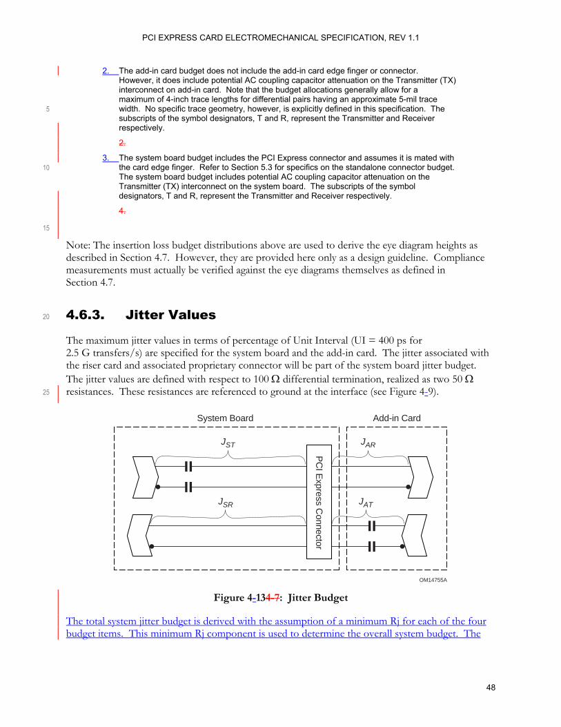
PCI EXPRESS CARD ELECTROMECHANICAL SPECIFICATION, REV 1.1
48
2. The add-in card budget does not include the add-in card edge finger or connector. However, it does include potential AC coupling capacitor attenuation on the Transmitter (TX) interconnect on add-in card. Note that the budget allocations generally allow for a maximum of 4-inch trace lengths for differential pairs having an approximate 5-mil trace width. No specific trace geometry, however, is explicitly defined in this specification. The 5 subscripts of the symbol designators, T and R, represent the Transmitter and Receiver respectively.
2.
3. The system board budget includes the PCI Express connector and assumes it is mated with the card edge finger. Refer to Section 5.3 for specifics on the standalone connector budget. 10 The system board budget includes potential AC coupling capacitor attenuation on the Transmitter (TX) interconnect on the system board. The subscripts of the symbol designators, T and R, represent the Transmitter and Receiver respectively.
4.
15
Note: The insertion loss budget distributions above are used to derive the eye diagram heights as described in Section 4.7. However, they are provided here only as a design guideline. Compliance measurements must actually be verified against the eye diagrams themselves as defined in Section 4.7.
4.6.3. Jitter Values 20
The maximum jitter values in terms of percentage of Unit Interval (UI = 400 ps for 2.5 G transfers/s) are specified for the system board and the add-in card. The jitter associated with the riser card and associated proprietary connector will be part of the system board jitter budget. The jitter values are defined with respect to 100 Ω differential termination, realized as two 50 Ω resistances. These resistances are referenced to ground at the interface (see Figure 4-9). 25
Add-in CardSystem Board
PC
I Express C
onnector
OM14755A
JST JAR
JSR JAT
Figure 4-134-7: Jitter Budget
The total system jitter budget is derived with the assumption of a minimum Rj for each of the four budget items. This minimum Rj component is used to determine the overall system budget. The
PCI EXPRESS CARD ELECTROMECHANICAL SPECIFICATION, REV 1.1
49
probability distribution of the Rj component is at the Bit Error Rate (BER) indicated and is Gaussian.
For any jitter distribution the total Tj must always be met at the BER. The Rj of the components are independent and convolve as the root sum square. Tradeoffs of Rj and Dj are allowed, provided the total Tj is always met. More information on the calculation of the system budget can be found 5 in PCI Express Jitter and BER.
Table 4-7: Total System Jitter Budget
Jitter Contribution Min Rj (ps) Max Dj (ps) Tj at BER 10-12 (ps) Tj at BER 10-6 (ps) Tx 2.8 60.6 100 87
Ref Clock 4.7 41.9 108 86 Media 0 90 90 90
Rx 2.8 120.6 160 147
Linear Total Tj: 458 410 Root Sum Square (RSS) Total Tj: 399.13 371.52
Notes:
1. RSS equation for BER 10-12 Tj = n
Dj∑ + 14.069 * 2
nRj∑
2. RSS equation for BER 10-6 Tj = nDj∑ + 9.507 * 2∑ nRj
10
PCI EXPRESS CARD ELECTROMECHANICAL SPECIFICATION, REV 1.1
50
Table 4-84-4: Allocation of Interconnect Jitter Budget
Jitter Parameter Jitter Budget Value (UI) Comments
PCI Express Add-in Card
J AR < 0.0575
J AT < 0.0650 Notes 1, 2
System Board and Connector
J ST < 0.1675 J SR < 0.1600 Notes 1, 3
Total Jitter J T < 0.225 Note 1
Notes: 1. All values are referenced to 100 Ω, realized as two 50 Ω resistances.
The jitter budget values include all possible crosstalk impacts (near-end and far-end) and potential mismatch of the actual interconnect with respect to the 100 Ω reference load. 5
The PCI Express Base Specification, Revision 1.1 allows an interconnect jitter budget of 0.3 225 UI (equivalent to 90 ps for a 400 ps Unit-Interval). The allocated jitter budget values in the table Table 4-7 and Table 4-8 directly correlate to the eye diagram widths in Section 4.7. Tradeoffs in terms of attenuation, crosstalk, and 10 mismatch can be made within the budget allocations specified. No additional guard band is specifically allocated.
As a guide for design and simulation, the following derivation of the budgets may be assumed: 0.75 UI is subtracted from 0.3 UI in order to account for near-end crosstalk and impedance mismatches. The 15 following jitter allocations are then assumed per differential pair: JAR = 0.035 UI; JAT = 0.045 UI; JSR = 0.18 UI; JST = 0.19 UI. according to the table. These allocation assumptions must also include any effects of far-end crosstalk.
2. All values are referenced to 100 Ω. The add-in card budget does not 20 include the add-in card edge finger or connector. However, it does include potential jitter from the AC coupling capacitors on the Transmitter (TX) interconnect of the add-in card. The budget allocations generally allow for a maximum of 4-inch trace lengths for differential pairs having an approximate 5-mil trace width. No specific 25 trace geometry, however, is explicitly defined in this specification. The subscripts of the symbol designators, T and R, represent the Transmitter and Receiver respectively.
3. All values are referenced to 100 Ω. The system board budget includes the PCI Express connector and assumes it is mated with the 30 card edge finger. Refer to Section 5.3 for specifics on the standalone connector budget. The system board budget includes potential jitter from the AC coupling capacitors on the Transmitter (TX) interconnect on the system board. The subscripts of the symbol designators, T and R, represent the Transmitter and Receiver respectively. 35
Note: The jitter budget distributions above are used to derive the eye diagram widths as described later in this Chapter chapter4. However, they are provided here only as a design guideline. Compliance measurements must actually be verified against the eye diagrams themselves as defined in Section 4.7.

PCI EXPRESS CARD ELECTROMECHANICAL SPECIFICATION, REV 1.1
51
4.6.4. Crosstalk
All add-in card designs must properly account for any crosstalk that may exist among the various pairs of differential signals. Crosstalk may be either near-end (NEXT) or far-end (FEXT). Each component can have potential impact on a design and must be planned for accordingly.
Note that the total maximum crosstalk that a Receiver component in Electrical Idle is required to 5 tolerate is < 65 mV as dictated by the Electrical Idle Detect Threshold in the PCI Express Base Specification, Revision 1.1. Additionally, crosstalk between differential pairs on the add-in card will influence and impact the data signals and any subsequent loss and jitter budgets as noted in Sections 4.6.2 and 4.6.3. Note that all eye diagrams in Section 4.7 must account for any and all crosstalk present. In order to limit crosstalk impacts and implications, it is recommended that the add-in card 10 limit the total amount of NEXT to a maximum of 50 mV.
All system boards interfacing with an add-in card must also properly account for crosstalk. The system board must also account for potential crosstalk that can occur on the printed circuit board as well as within the connector itself (see Section 5.3).
4.6.5. Lane-to-Lane Skew 15
The skew at any point is measured using zero crossings of differential voltage of the compliance pattern, while simultaneously transmitting on all physical Lanes. The compliance pattern is defined in the PCI Express Base Specification, Revision 1.1.

PCI EXPRESS CARD ELECTROMECHANICAL SPECIFICATION, REV 1.1
52
Table 4-104-5: Allowable Interconnect Lane-to-Lane Skew
Skew Parameter Symbol Skew Values Comments Total Interconnect Skew TS 1.6 ns This does not include
Transmitter output skew, LTX-SKEW (specified in the PCI Express Base Specification, Revision 1.1). The total skew at the Receiver (ST + LTX-SKEW ) is smaller than LRX-SKEW (specified in the PCI Express Base Specification, Revision 1.1) to minimize latency for this add-in card topology.
PCI Express Add-in Card AS 0.35 ns Estimates about a 2-inch trace
length delta on FR4 boards.
System Board sS 1.25 ns Estimates about a 7-inch trace
length delta on FR4 boards.
4.6.6. Equalization
To reduce ISI, 3.5 dB (+/-0.5 dB) below the first bit de-emphasis in the Transmitter is required for the add-in card and the system board. For implementation details, refer to Chapter 4 in the PCI Express Base Specification, Revision 1.1.
4.6.7. Skew within Within the Differential Pair 5
The skew within the differential pair gives rise to a common-mode signal component, which can, in turn, increase Electromagnetic Interference (EMI). The differential pair should be routed such that the skew within differential pairs is less than 5 mils for the add-in card and 10 mils for the system board.
4.7. Eye Diagrams at the Add-in Card Interface 10
The eye diagrams defined in this section represent the compliance eye diagrams that must be met for both the add-in card and a system board interfacing with such an add-in card. The specific measurement requirements (probe test points, calibrated system board specifics, etc.) for compliance of physical components are to be specified in a separatethe and unique PHY Electrical Test Considerations for PCI Express Architecture Compliance Testing document. A sample size of 106 UI is 15 assumed for the eye diagram measurements. These compliance eye diagrams with BER of 10-12 can also be used for simulation by Compliance eye diagram validation in a simulation environment is possible following the guidelines explained in Section 4.6.

PCI EXPRESS CARD ELECTROMECHANICAL SPECIFICATION, REV 1.1
53
4.7.1. Add-in Card Transmitter Path Compliance Eye-Diagram
The eye-diagram for the add-in card’s Transmitter path compliance is defined in Table 4-12 and Figure 4-15.
Table 4-124-6: Add-in Card Transmitter Path Compliance Eye Requirements
Parameter Value Comments
VTXA
VTXA_d
>= 514 mV
>= 360 mV
Notes 1, 2, 5
Notes 1, 2, 5
TTXA
JTXA-MEDIAN-to-MAX-JITTER
>= 287 ps
<= 56.5 ps
Notes 1, 3, 5
Notes 1, 4, 5
Notes: 5
1. An ideal reference clock without jitter is assumed for this specification. All Links are assumed active while generating this eye diagram.
2. Transition and non-transition bits must be distinguished in order to measure compliance against the de-emphasized voltage level (VTXA_d). V TXA
and VTXA_d are minimum differential peak-peak output voltages. 10
3. T TXA
is the minimum eye width. The sample size for this measurement is 106 UI. This value can be reduced to 274 ps for simulation purpose at BER 10-12.
4. JTXA-MEDIAN-to-MAX-JITTER is the maximum median-to-max jitter outlier as defined in the PCI Express Base Specification, Revision 1.1. The sample size for this measurement is 106 UI. This value can be increased to 63 ps for simulation 15 purpose at BER 10-12.
5. The values in Table 4-12 are referenced to an ideal 100 Ω differential load at the end of the interconnect path at the edge-finger boundary on the add-in card (see Figure 4-9). The eye diagram is defined and centered with respect to the jitter median. Exact conditions required for verifying compliance while 20 generating this eye diagram are given in the PHY Electrical Test Considerations for PCI Express Architecture document.
Parameter Value Notes
VtxA
VtxA_d
TtxA
>= 514 mV
>= 360 mV
>= 237 ps
All Links are assumed active while generating this eye diagram. Transition and non-transition bits must be distinguished in order to measure compliance against the de-emphasized voltage level (VtxA_d).
Note: The values in Table 4-6 are referenced to an ideal 100 Ω differential load at the end of the interconnect path at the edge-finger boundary on the add-in card. Exact conditions required for verifying compliance while generating this eye diagram are to be given in the compliance testing 25 document. The eye diagram is defined and centered with respect to the jitter median. The jitter median should be calculated across any 250 consecutive UIs. The maximum jitter outlier should be no greater than 118.5 ps away from the jitter median.
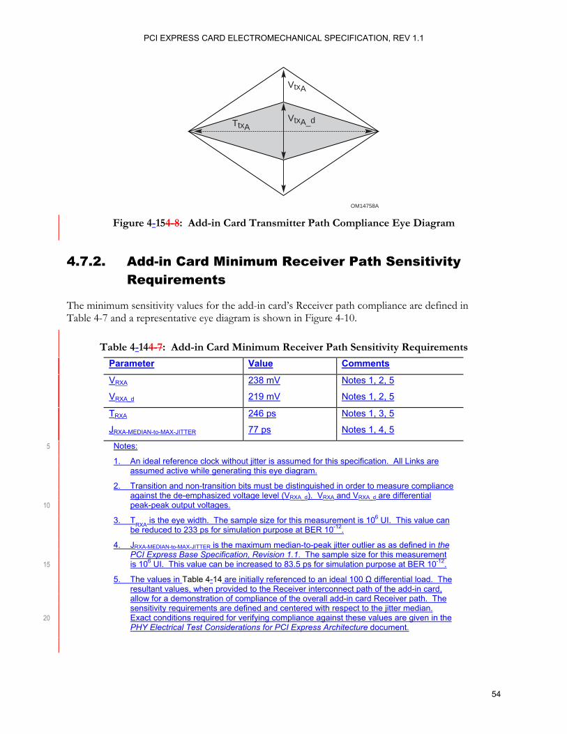
PCI EXPRESS CARD ELECTROMECHANICAL SPECIFICATION, REV 1.1
54
OM14758A
TtxA
VtxA
VtxA_d
Figure 4-154-8: Add-in Card Transmitter Path Compliance Eye Diagram
4.7.2. Add-in Card Minimum Receiver Path Sensitivity Requirements
The minimum sensitivity values for the add-in card’s Receiver path compliance are defined in Table 4-7 and a representative eye diagram is shown in Figure 4-10.
Table 4-144-7: Add-in Card Minimum Receiver Path Sensitivity Requirements
Parameter Value Comments
VRXA
VRXA_d
238 mV
219 mV
Notes 1, 2, 5
Notes 1, 2, 5
TRXA
JRXA-MEDIAN-to-MAX-JITTER
246 ps
77 ps
Notes 1, 3, 5
Notes 1, 4, 5
Notes: 5
1. An ideal reference clock without jitter is assumed for this specification. All Links are assumed active while generating this eye diagram.
2. Transition and non-transition bits must be distinguished in order to measure compliance against the de-emphasized voltage level (VRXA_d). VRXA and VRXA_d are differential peak-peak output voltages. 10
3. T RXA
is the eye width. The sample size for this measurement is 106 UI. This value can be reduced to 233 ps for simulation purpose at BER 10-12.
4. JRXA-MEDIAN-to-MAX-JITTER is the maximum median-to-peak jitter outlier as as defined in the PCI Express Base Specification, Revision 1.1. The sample size for this measurement is 106 UI. This value can be increased to 83.5 ps for simulation purpose at BER 10-12. 15
5. The values in Table 4-14 are initially referenced to an ideal 100 Ω differential load. The resultant values, when provided to the Receiver interconnect path of the add-in card, allow for a demonstration of compliance of the overall add-in card Receiver path. The sensitivity requirements are defined and centered with respect to the jitter median. Exact conditions required for verifying compliance against these values are given in the 20 PHY Electrical Test Considerations for PCI Express Architecture document.
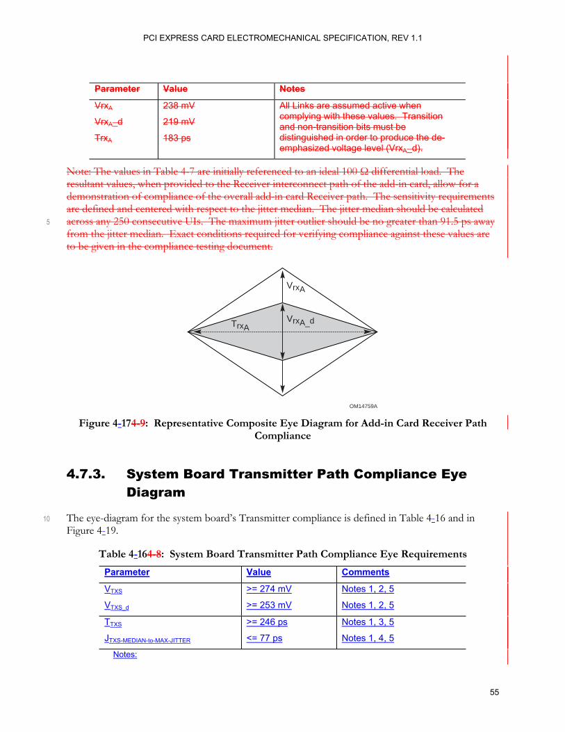
PCI EXPRESS CARD ELECTROMECHANICAL SPECIFICATION, REV 1.1
55
Parameter Value Notes
VrxA
VrxA_d
TrxA
238 mV
219 mV
183 ps
All Links are assumed active when complying with these values. Transition and non-transition bits must be distinguished in order to produce the de-emphasized voltage level (VrxA_d).
Note: The values in Table 4-7 are initially referenced to an ideal 100 Ω differential load. The resultant values, when provided to the Receiver interconnect path of the add-in card, allow for a demonstration of compliance of the overall add-in card Receiver path. The sensitivity requirements are defined and centered with respect to the jitter median. The jitter median should be calculated across any 250 consecutive UIs. The maximum jitter outlier should be no greater than 91.5 ps away 5 from the jitter median. Exact conditions required for verifying compliance against these values are to be given in the compliance testing document.
OM14759A
TrxA
VrxA
VrxA_d
Figure 4-174-9: Representative Composite Eye Diagram for Add-in Card Receiver Path
Compliance
4.7.3. System Board Transmitter Path Compliance Eye Diagram
The eye-diagram for the system board’s Transmitter compliance is defined in Table 4-16 and in 10 Figure 4-19.
Table 4-164-8: System Board Transmitter Path Compliance Eye Requirements Parameter Value Comments
VTXS
VTXS_d
>= 274 mV
>= 253 mV
Notes 1, 2, 5
Notes 1, 2, 5
TTXS
JTXS-MEDIAN-to-MAX-JITTER
>= 246 ps
<= 77 ps
Notes 1, 3, 5
Notes 1, 4, 5
Notes:

PCI EXPRESS CARD ELECTROMECHANICAL SPECIFICATION, REV 1.1
56
1. An ideal reference clock without jitter is assumed for this specification. All Links are assumed active while generating this eye diagram.
2. Transition and non-transition bits must be distinguished in order to measure compliance against the de-emphasized voltage level (VTXS_d). VTXS and VTXS_d are minimum differential peak-peak output voltages. 5
3. T TXS is the minimum eye width. The sample size for this measurement is 106 UI. This value can be reduced to 233 ps for simulation purpose at BER 10-12.
4. JTXS-MEDIAN-to-MAX-JITTER is the maximum median-to-max jitter outlier as defined in the PCI Express Base Specification, Revision 1.1. The sample size for this measurement is 106 UI, This value can be increased to 83.5 ps for simulation purpose at BER 10-12. 10
5. The values in Table 4-16 are referenced to an ideal 100 Ω differential load at the end of the interconnect path at the edge-finger boundary on the add-in card when mated with a connector (see Figure 4-9). The eye diagram is defined and centered with respect to the jitter median. Exact conditions required for verifying compliance while generating this eye diagram are given in the PHY Electrical Test Considerations for PCI Express 15 Architecture document.
Parameter Value Notes
VtxS
VtxS_d
TtxS
>= 274 mV
>= 253 mV
>= 183 ps
All Links are assumed active while generating this eye diagram. Transition and non-transition bits must be distinguished in order to measure compliance against the de-emphasized voltage level (TtxS_d).
Note: The values in Table 4-8 are referenced to an ideal 100 Ω differential load at the end of the interconnect path at the isolated edge-finger boundary of an add-in card when mated with a 20 connector. The eye diagram is defined and centered with respect to the jitter median. The jitter median should be calculated across any 250 consecutive UIs. The maximum jitter outlier should be no greater than 91.5 ps away from the jitter median.
Exact conditions required for verifying compliance while generating this eye diagram are to be given in the compliance testing document. 25
A-0335
TtxS
VtxS
VtxS_d
Figure 4-194-10: System Board Transmitter Path Composite Compliance Eye Diagram
It is not always possible to measure the System Board Transmitter Path Eye Diagrams with an ideal reference clock. In this case, a two port measurement can adjust the measurement for the non-ideal
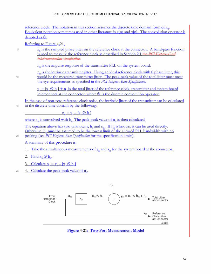
PCI EXPRESS CARD ELECTROMECHANICAL SPECIFICATION, REV 1.1
57
reference clock. The notation in this section assumes the discrete time domain form of xn. Equivalent notation sometimes used in other literature is x(n) and x[n]. The convolution operator is denoted as ⊗.
Referring to Figure 4-21, xn is the sampled phase jitter on the reference clock at the connector. A band-pass function 5 is used to measure the reference clock as described in Section 2.1.the PCI Express Card Electromechanical Specification.
hn is the impulse response of the transmitter PLL on the system board.
nn is the intrinsic transmitter jitter. Using an ideal reference clock with 0 phase jitter, this would be the measured transmitter jitter. The peak-peak value of the total jitter must meet 10 the eye requirements as specified in the PCI Express Base Specification.
yn = [xn ⊗ hn] + nn is the total jitter of the reference clock, transmitter and system board interconnect at the connector, where ⊗ is the discrete convolution operator.
In the case of non-zero reference clock noise, the intrinsic jitter of the transmitter can be calculated in the discrete time domain by the following: 15
nn = yn – [xn ⊗ hn]
where xn is convolved with hn. The peak-peak value of nn is then calculated.
The equation above has two unknowns, hn and nn. If hn is known, it can be used directly. Otherwise, hn must be assumed to be the lowest limit of the allowed PLL bandwidth with no peaking (see PCI Express Base Specification for the specification limits). 20
A summary of this procedure is:
1. Take the simultaneous measurements of yn and xn for the system board at the connector.
2. Find xn ⊗ hn.
3. Calculate nn = yn – [xn ⊗ hn]
4. Calculate the peak-peak value of nn. 25
A-0465
FromReference
Clock
Total Jitterat Connector
ReferenceClock Jitterat Connector
hn +xn ⊗ hn yn = xn ⊗ hn + nnxn
nn
xn
Figure 4-21: Two-Port Measurement Model
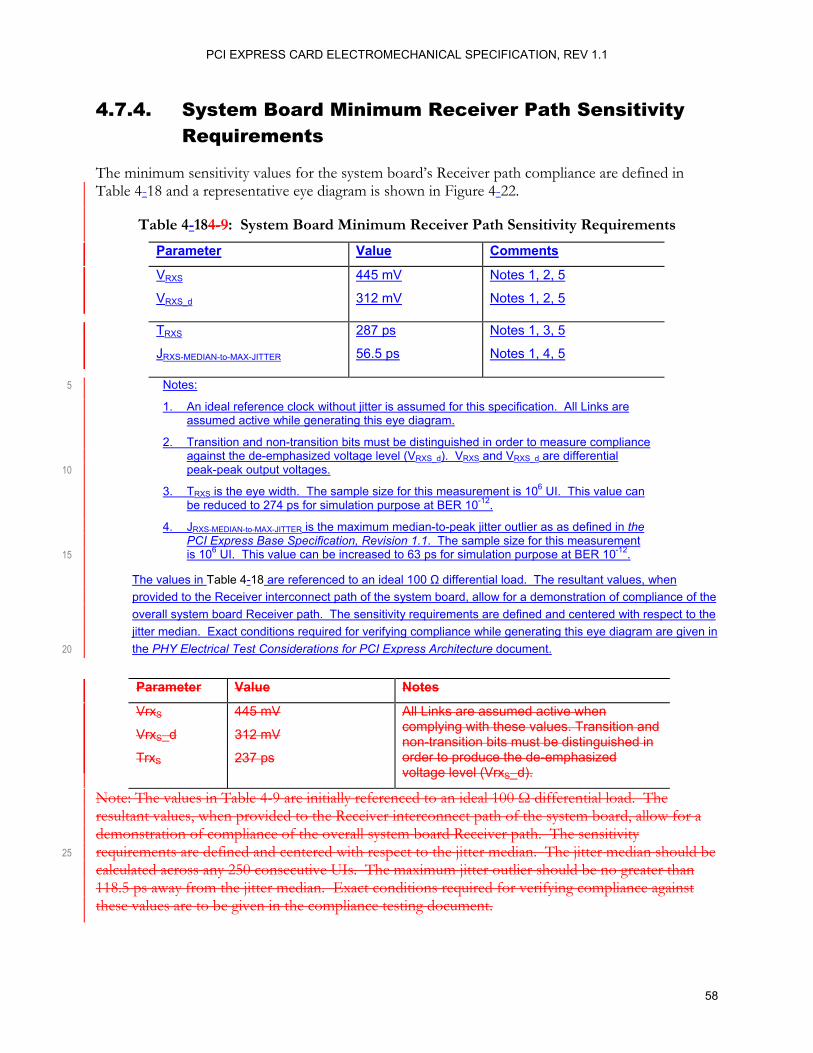
PCI EXPRESS CARD ELECTROMECHANICAL SPECIFICATION, REV 1.1
58
4.7.4. System Board Minimum Receiver Path Sensitivity Requirements
The minimum sensitivity values for the system board’s Receiver path compliance are defined in Table 4-18 and a representative eye diagram is shown in Figure 4-22.
Table 4-184-9: System Board Minimum Receiver Path Sensitivity Requirements
Parameter Value Comments
VRXS
VRXS_d
445 mV
312 mV
Notes 1, 2, 5
Notes 1, 2, 5
TRXS
JRXS-MEDIAN-to-MAX-JITTER
287 ps
56.5 ps
Notes 1, 3, 5
Notes 1, 4, 5
Notes: 5
1. An ideal reference clock without jitter is assumed for this specification. All Links are assumed active while generating this eye diagram.
2. Transition and non-transition bits must be distinguished in order to measure compliance against the de-emphasized voltage level (VRXS_d). VRXS and VRXS_d are differential peak-peak output voltages. 10
3. TRXS is the eye width. The sample size for this measurement is 106 UI. This value can be reduced to 274 ps for simulation purpose at BER 10-12.
4. JRXS-MEDIAN-to-MAX-JITTER is the maximum median-to-peak jitter outlier as as defined in the PCI Express Base Specification, Revision 1.1. The sample size for this measurement is 106 UI. This value can be increased to 63 ps for simulation purpose at BER 10-12. 15
The values in Table 4-18 are referenced to an ideal 100 Ω differential load. The resultant values, when provided to the Receiver interconnect path of the system board, allow for a demonstration of compliance of the overall system board Receiver path. The sensitivity requirements are defined and centered with respect to the jitter median. Exact conditions required for verifying compliance while generating this eye diagram are given in the PHY Electrical Test Considerations for PCI Express Architecture document. 20
Parameter Value Notes
VrxS
VrxS_d
TrxS
445 mV
312 mV
237 ps
All Links are assumed active when complying with these values. Transition and non-transition bits must be distinguished in order to produce the de-emphasized voltage level (VrxS_d).
Note: The values in Table 4-9 are initially referenced to an ideal 100 Ω differential load. The resultant values, when provided to the Receiver interconnect path of the system board, allow for a demonstration of compliance of the overall system board Receiver path. The sensitivity requirements are defined and centered with respect to the jitter median. The jitter median should be 25 calculated across any 250 consecutive UIs. The maximum jitter outlier should be no greater than 118.5 ps away from the jitter median. Exact conditions required for verifying compliance against these values are to be given in the compliance testing document.
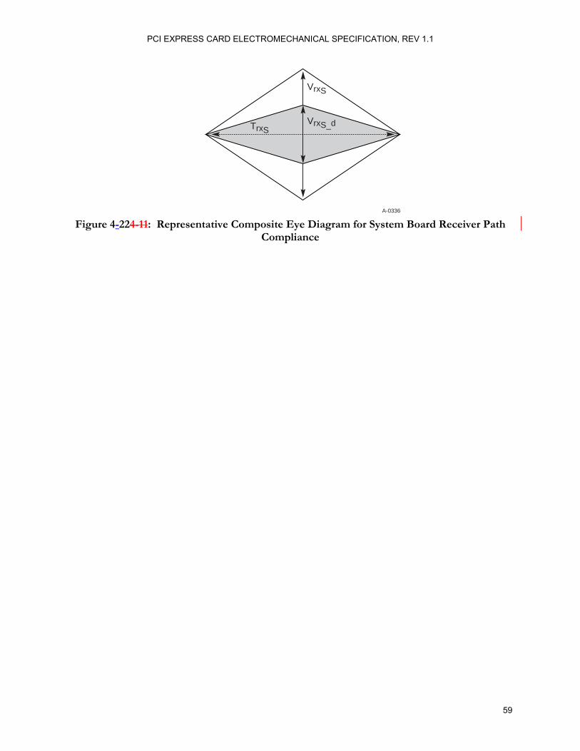
PCI EXPRESS CARD ELECTROMECHANICAL SPECIFICATION, REV 1.1
59
A-0336
TrxS
VrxS
VrxS_d
Figure 4-224-11: Representative Composite Eye Diagram for System Board Receiver Path
Compliance

PCI EXPRESS CARD ELECTROMECHANICAL SPECIFICATION, REV 1.1
60
5. Connector Specification A family of PCI Express vertical edge card connectors supports x1, x4, x8, and x16 Link widths to suit different bandwidth requirements. These connectors support the PCI Express signal and power requirements, as well as auxiliary signals used to facilitate the interface between system board and add-in card hardware. This chapter defines the connector mating interfaces and footprints, as well 5 as the electrical, mechanical, and environmental requirements.
5.1. Connector Pinout Table 5-1 shows the pinout definition for the x1, x4, x8, and x16 PCI Express connectors. The auxiliary pins are identified in the shaded areas.
Table 5-15-1: PCI Express Connectors Pinout
Side B Side A Pin#
Name Description Name Description
1 +12V 12 V power PRSNT1# Hot-Plug presence detect
2 +12V 12 V power +12V 12 V power
3 +12VRSVD 12 V powerReserved +12V 12 V power
4 GND Ground GND Ground
5 SMCLK SMBus (System Management Bus) clock
JTAG2 TCK (Test Clock), clock input for JTAG interface
6 SMDAT SMBus (System Management Bus) data
JTAG3 TDI (Test Data Input)
7 GND Ground JTAG4 TDO (Test Data Output)
8 +3.3V 3.3 V power JTAG5 TMS (Test Mode Select)
9 JTAG1 TRST# (Test Reset) resets the JTAG interface
+3.3V 3.3 V power
10 3.3Vaux 3.3 V auxiliary power +3.3V 3.3 V power
11 WAKE# Signal for Link reactivation
PERST# Fundamental reset
5

PCI EXPRESS CARD ELECTROMECHANICAL SPECIFICATION, REV 1.1
61
Side B Side A Pin#
Name Description Name Description
Mechanical key
12 RSVD Reserved GND Ground
13 GND Ground REFCLK+
14 PETp0 REFCLK-
Reference clock (differential pair)
15 PETn0
Transmitter differential pair, Lane 0
GND Ground
16 GND Ground PERp0
17 PRSNT2# Hot-Plug presence detect PERn0
Receiver differential pair, Lane 0
18 GND Ground GND Ground
End of the x1 connector
19 PETp1 RSVD
20 PETn1
Transmitter differential pair, Lane 1
GND Ground
21 GND Ground PERp1
22 GND Ground PERn1
Receiver differential pair, Lane 1
23 PETp2 GND Ground
24 PETn2
Transmitter differential pair, Lane 2
GND Ground
25 GND Ground PERp2
26 GND Ground PERn(2)
Receiver differential pair, Lane 2
27 PETp3 GND Ground
28 PETn0
Transmitter differential pair, Lane 3
GND Ground
29 GND Ground PERp3
30 RSVD Reserved PERn3
Receiver differential pair, Lane 3
31 PRSNT2# Hot-Plug presence detect GND Ground
32 GND Ground RSVD Reserved
End of the x4 connector
33 PETp4 RSVD Reserved
34 PETn4)
Transmitter differential pair, Lane 4
GND Ground
35 GND Ground PERp4
36 GND Ground PERn4
Receiver differential pair, Lane 4
37 PETp5 GND Ground
38 PETn5
Transmitter differential pair, Lane 5
GND Ground
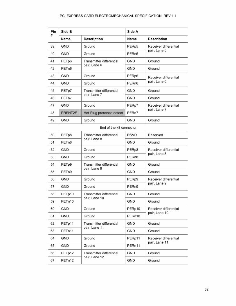
PCI EXPRESS CARD ELECTROMECHANICAL SPECIFICATION, REV 1.1
62
Side B Side A Pin#
Name Description Name Description
39 GND Ground PERp5
40 GND Ground PERn5
Receiver differential pair, Lane 5
41 PETp6 GND Ground
42 PETn6
Transmitter differential pair, Lane 6
GND Ground
43 GND Ground PERp6
44 GND Ground PERn6
Receiver differential pair, Lane 6
45 PETp7 GND Ground
46 PETn7
Transmitter differential pair, Lane 7
GND Ground
47 GND Ground PERp7
48 PRSNT2# Hot-Plug presence detect PERn7
Receiver differential pair, Lane 7
49 GND Ground GND Ground
End of the x8 connector
50 PETp8 RSVD Reserved
51 PETn8
Transmitter differential pair, Lane 8
GND Ground
52 GND Ground PERp8
53 GND Ground PERn8
Receiver differential pair, Lane 8
54 PETp9 GND Ground
55 PETn9
Transmitter differential pair, Lane 9
GND Ground
56 GND Ground PERp9
57 GND Ground PERn9
Receiver differential pair, Lane 9
58 PETp10 GND Ground
59 PETn10
Transmitter differential pair, Lane 10
GND Ground
60 GND Ground PERp10
61 GND Ground PERn10
Receiver differential pair, Lane 10
62 PETp11 GND Ground
63 PETn11
Transmitter differential pair, Lane 11
GND Ground
64 GND Ground PERp11
65 GND Ground PERn11
Receiver differential pair, Lane 11
66 PETp12 GND Ground
67 PETn12
Transmitter differential pair, Lane 12
GND Ground
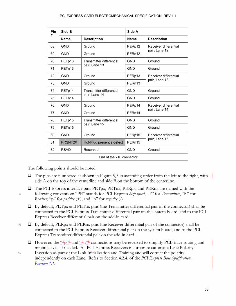
PCI EXPRESS CARD ELECTROMECHANICAL SPECIFICATION, REV 1.1
63
Side B Side A Pin#
Name Description Name Description
68 GND Ground PERp12
69 GND Ground PERn12
Receiver differential pair, Lane 12
70 PETp13 GND Ground
71 PETn13
Transmitter differential pair, Lane 13
GND Ground
72 GND Ground PERp13
73 GND Ground PERn13
Receiver differential pair, Lane 13
74 PETp14 GND Ground
75 PETn14
Transmitter differential pair, Lane 14
GND Ground
76 GND Ground PERp14
77 GND Ground PERn14
Receiver differential pair, Lane 14
78 PETp15 GND Ground
79 PETn15
Transmitter differential pair, Lane 15
GND Ground
80 GND Ground PERp15
81 PRSNT2# Hot-Plug presence detect PERn15
Receiver differential pair, Lane 15
82 RSVD Reserved GND Ground
End of the x16 connector The following points should be noted:
The pins are numbered as shown in Figure 5-3 in ascending order from the left to the right, with side A on the top of the centerline and side B on the bottom of the centerline.
The PCI Express interface pins PETpx, PETnx, PERpx, and PERnx are named with the following convention: “PE” stands for PCI Express high speed, “T” for Transmitter, “R” for 5 Receiver, “p” for positive (+), and “n” for negative (-). By default, PETpx and PETnx pins (the Transmitter differential pair of the connector) shall be
connected to the PCI Express Transmitter differential pair on the system board, and to the PCI Express Receiver differential pair on the add-in card.
By default, PERpx and PERnx pins (the Receiver differential pair of the connector) shall be 10 connected to the PCI Express Receiver differential pair on the system board, and to the PCI Express Transmitter differential pair on the add-in card.
However, the “"p”" and “"n”" connections may be reversed to simplify PCB trace routing and minimize vias if needed. All PCI-Express Receivers incorporate automatic Lane Polarity Inversion as part of the Link Initialization and Training and will correct the polarity 15 independently on each Lane. Refer to Section 4.2.4. of the PCI Express Base Specification, Revision 1.1.
PCI EXPRESS CARD ELECTROMECHANICAL SPECIFICATION, REV 1.1
64
If the component on the system board or add-in card does not support the optional PCI Express Lane Reversal functions, they must connect each Transmitter and Receiver Lane to the add-in card connector lanes as shown in Table 5-1. For example, a x4 component must connect Lane 0 to 0, Lane 1 to 1, Lane 2 to 2, and Lane 3 to 3.
If the component on the system board or add-in card supports the optional PCI Express Lane 5 Reversal function, it may connect each Transmitter and Receiver Lane to the add-in card connector lanes as shown in Table 5-1 or it may connect the Transmitter and Receiver lanes using a reversed Lane ordering. Either Lane ordering may be used to simplify PCB trace routing and minimize vias. However, the transmitting and receiving lanes must be connected with the same Lane ordering. For example, a x4 component may connect Lane 0 to 0, Lane 1 to 1, Lane 10 2 to 2, and Lane 3 to 3 or it may connect Lane 0 to 3, Lane 1 to 2, Lane 2 to 1, and Lane 3 to 0.
The connectors and the add-in cards are keyed such that smaller add-in cards can be put in larger connectors. For example, an x1 card can be inserted into the x4, x8, and x16 connectors. This is referred to as up-plugging.
Adjacent differential pairs are separated by two ground pins to manage the connector crosstalk. 15
See Chapter 2 for auxiliary signals description and implementation, except the +3.3Vaux and PRSNT1# and PRSNT2# pins. The requirements for +3.3Vaux are discussed in Chapter 4 and presence detect is discussed in Chapter 3.
PRSNT1# and PRSNT2# pins are for card presence detect. One present detect pin at each end of a connector guarantees that at least one of the present detect pins is last-mate/first-break. 20 More than two PRSNT2# pins in the x4, x8, and x16 PCI Express connectors are for the purpose of supporting up-plugging. See Chapter 3 for detailed discussions on presence detect.
The sequential mating for Hot-Plug is accomplished by staggering the edge fingers on the add-in card, as shown in Section 5.2. Detailed requirements on Hot-Plug are covered in Chapter 3.
Power pins (+3.3V, +3.3Vaux, and +12V) are defined based on the PCI Express power delivery 25 requirements specified in Chapter 4, with the connector contact carrying capability being 1.1 A per pin. The power that goes through the connector shall not exceed the maximum power specified for a given add-in card size, as defined in Table 4-3.
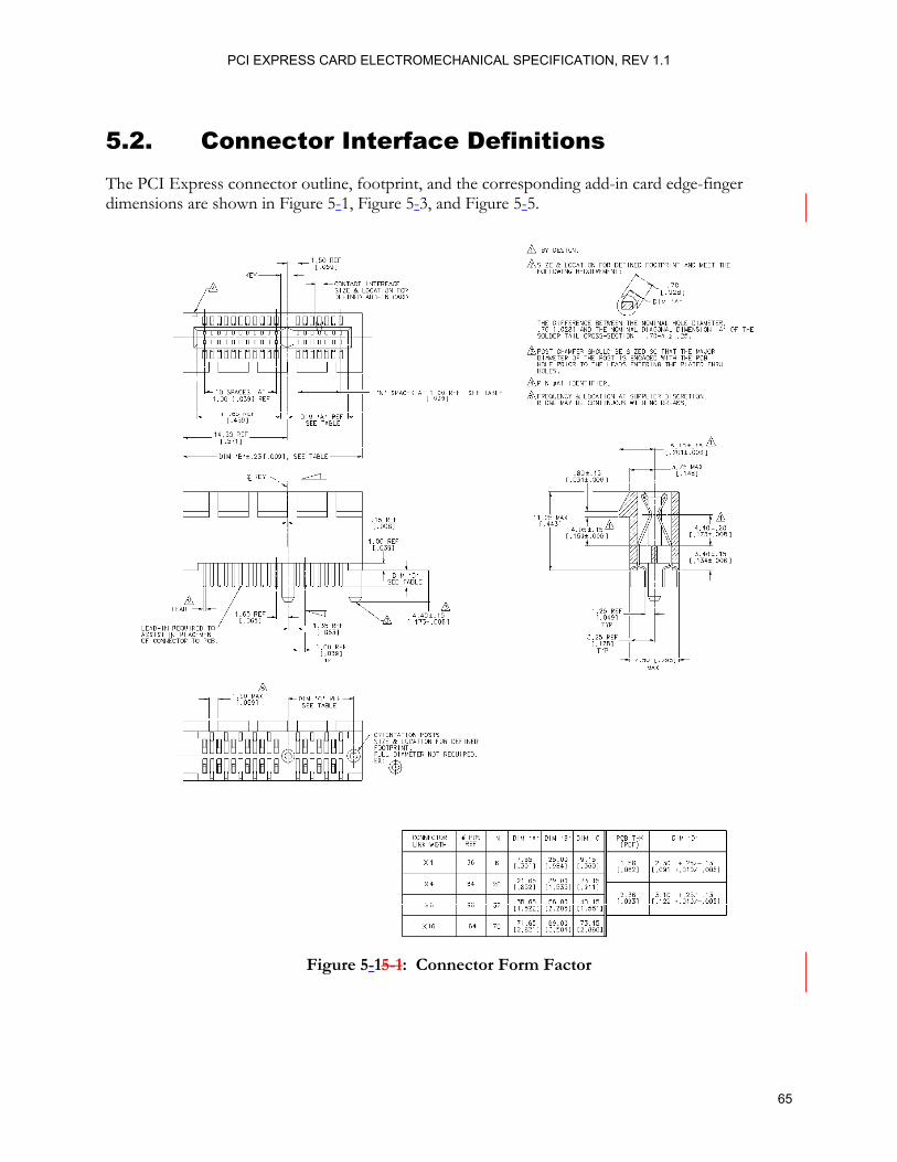
PCI EXPRESS CARD ELECTROMECHANICAL SPECIFICATION, REV 1.1
65
5.2. Connector Interface Definitions The PCI Express connector outline, footprint, and the corresponding add-in card edge-finger dimensions are shown in Figure 5-1, Figure 5-3, and Figure 5-5.
Figure 5-15-1: Connector Form Factor

PCI EXPRESS CARD ELECTROMECHANICAL SPECIFICATION, REV 1.1
66
Figure 5-35-2: Recommended Footprint

PCI EXPRESS CARD ELECTROMECHANICAL SPECIFICATION, REV 1.1
67
Figure 5-55-3: Add-in Card Edge-Finger Dimensions
PCI EXPRESS CARD ELECTROMECHANICAL SPECIFICATION, REV 1.1
68
The following points should be noted:
The connector has a 1.00 mm contact pitch.
The contact shall be pre-loaded, similar to the PCI connector.
The connector footprint (Figure 5-3) requires two 2.35 mm diameter location holes, working with either plastic pegs/posts or metal board locks. Metal board locks are allowed, although 5 Figure 5-1 shows only the plastic pegs on the connector housing.
Figure 5-5 defines only the mating interface related dimensions. Other add-in card dimensions are defined in Chapter 6.
The PRSNT1# and PRSNT2# pins shown in Figure 5-5 are 1 mm shorter than the other fingers. Those pins are designated as A1, B17, B31, B48, and B81, where applicable. No plating 10 tie bar is allowed underneath the PRSNT1# and PRSNT2# pins because those pins are meant to be last-mate and first-break.
As shown in Figure 5-1, a ridge feature is defined on the top of the connector housing on one side. This feature can be used to facilitate card retention. A retention clip may be mounted on an add-in card and latched on the ridge. 15
Two types of add-in cards must be “retention ready”:
• Graphics cards
• x1, x4, x8, or x16 I/O cards that in the judgment of the OEM or card manufacturers have sufficient weight or length that the card may need an additional retention point for stability
Retention ready means that the add-in card manufacturer must have selected (or created) a 20 retention mechanism and made provisions on the card to facilitate the retention mechanism. The reference retention mechanism designs and related component keep-out or height restriction areas are defined in the PCI Express Graphics Card Thermal Mechanical Design Guidelines.
The full-length card 321.00 mm (12.283 inches) long is considered retention ready. The mounting holes on one end of the full-length card allow the optional PCI card retainer to be 25 installed to secure the card. See Section 6.1.
Detailed connector contact and housing designs are up to each connector vendor, as long as the requirements of form, fit, and function are met.

PCI EXPRESS CARD ELECTROMECHANICAL SPECIFICATION, REV 1.1
69
5.3. Signal Integrity Requirements and Test Procedures
A common electrical test fixture is specified and used for evaluating connector signal integrity. The test fixture will have 6-mil wide 50-Ω single ended traces that must be uncoupled. The impedance variation of those traces shall be controlled within ±5%. Refer to the PCI Express Connector High 5 Speed Electrical Test Procedure for detailed discussions on the test fixture.
Detailed testing procedures, such as the vector network analyzer settings, operation, and calibration are specified in the PCI Express Connector High Speed Electrical Test Procedure. This document should be used in conjunction with the standard test fixture.
For the insertion loss and return loss tests, the measurement shall include 1.2-inch long PCB traces 10 (0.6 inches on the system board and 0.6 inches on the add-in card). Note that the edge finger pad is not counted as the add-in card PCB trace. It is considered to be part of the connector interface. The 1.2-inch PCB trace included in the connector measurement is a part of the trace length allowed on the system board. See Section 4.6 for a discussion of the electrical budget.
Either single ended measurements that are processed to extract the differential characteristics or true 15 differential measurements are allowed. The detailed definition and description of the test fixture and the measurement procedures are provided separately in a document entitled PCI Express Connector High Speed Electrical Test Procedure. An additional consideration for the connector electrical performance is the connector-to-system board and the connector-to-add-in-card launches. The connector through hole pad and anti-pad 20 sizes shall follow good electrical design practices to minimize impedance discontinuity.The connector through hole pad and anti-pad sizes, as well as trace layout on the system board shall follow the recommendations in the PCI Express Electrical Design Guidelines. On the add-in card, the ground and power planes underneath the PCI Express high-speed signals (edge fingers) shall be removed. Otherwise the edge fingers will have too much capacitance and greatly degrade connector 25 performance. A more detailed discussion on the add-in card electrical design can be found in the PCI Express Connector High Speed Electrical Test Procedure and the PCI Express Electrical Design Guidelines.
PCI EXPRESS CARD ELECTROMECHANICAL SPECIFICATION, REV 1.1
70
Table 5-3 lists the electrical signal integrity parameters, requirements, and test procedures.
Table 5-35-2: Signal Integrity Requirements and Test Procedures
Parameter Procedure Requirements
Insertion Loss (IL) EIA 364-101
The EIA standard must be used with the following considerations:
1. The step-by-step measurement procedure is outlined in the PCI Express Connector High Speed Electrical Test Procedure document (see Note 1 below).
2. A common test fixture for connector characterization shall be used.
3. This is a differential insertion loss requirement. Either true differential measurements must be made or post processing of the single ended measurements must be done to extract the differential characteristics of the connector. The methodology of doing so is covered in the PCI Express Connector High Speed Electrical Test Procedure document (Note 1).
1 dB max up to 1.25 GHz; ≤ [1.6*(F-1.25)+1] dB for 1.25 GHz < F ≤ 3.75 GHz (for example, ≤5 dB at F = 3.75 GHz).
Return Loss (RL) EIA 364-108
The EIA standard must be used with the following considerations:
1. The step-by-step measurement procedure is outlined in the PCI Express Connector High Speed Electrical Test Procedure document (Note 1).
2. A common test fixture for connector characterization shall be used.
3. This is a differential return loss requirement. Either true differential measurements must be made or post processing of the single ended measurements must be done to extract the differential characteristics of the connector. The methodology of doing so is covered in the PCI Express Connector High Speed Electrical Test Procedure document (Note 1).
≤ -12 dB up to 1.3 GHz; ≤ -7 dB up to 2 GHz; ≤ -4 dB up to 3.75 GHz
Intra-pair Skew Intra-pair skew must be achieved by design; measurement not required.
5 ps max
PCI EXPRESS CARD ELECTROMECHANICAL SPECIFICATION, REV 1.1
71
Parameter Procedure Requirements
Crosstalk: NEXT
EIA 364-90
The EIA standard must be used with the following considerations:
1. The crosstalk requirement is with respect to all the adjacent differential pairs including the crosstalk from opposite sides of the connector, as illustrated in Figure 5-7. This is reflected in the measurement procedure.
2. The step-by-step measurement procedure is outlined in the PCI Express Connector High Speed Electrical Test Procedure document.
3. A common test fixture for connector characterization shall be used.
4. This is a differential crosstalk requirement between a victim differential signal pair and all of its adjacent differential signal pairs. Either true differential measurements must be made or post processing of the single ended measurements must be done to extract the differential crosstalk of the connector. The methodology of doing so is covered in the PCI Express Connector High Speed Electrical Test Procedure document (see Note 1 below).
-32 dB max up to 1.25 GHz; ≤ -[32-2.4*(F-1.25)] dB for 1.25 GHz < F ≤ 3.75 GHz (for example, ≤ -26 dB at F = 3.75 GHz)
Jitter By design; measurement not required. 10 ps max
Notes: 1. The PCI Express Connector High Speed Electrical Test Procedure is available separately. 2. A network analyzer is required. Differential measurements require the use of a two port (or a four port) network
analyzer to measure the connector. The differential parameters may be measured directly if the equipment supports “True” differential excitation (“True” differential excitation is the simultaneous application of a signal to 5 one line of the pair and a 180 degree phase shifted version of the signal to the second line of the pair). If single ended measurements are made, the differential connector parameters must be derived from the single ended measurements as defined in the PCI Express Connector High Speed Electrical Test Procedure.
3.If differential measurements are made directly by application of differential signals, the equipment must use phase matched fixturing. The fixturing skew and measurement cabling should be verified to be <1 ps on a TDR. 10
4.3. The connector shall be targeted for a 100 Ω differential impedance.
PCI EXPRESS CARD ELECTROMECHANICAL SPECIFICATION, REV 1.1
72
In Figure 5-7, pairs marked as 11-9, 5-7, 15-13, and 17-19 are the adjacent pairs with respect to the victim pair 1-3.
OM14761
15 13 17 19
11 9 1 3
Victim PairNeed to Terminate All Ports
5 7
Figure 5-75-4: Illustration of Adjacent Pairs
5.4. Connector Environmental and Other Requirements
5.4.1. Environmental Requirements 5
Connector environmental tests shall follow EIA-364-1000.01, Environmental Test Methodology for Assessing the Performance of Electrical Connectors and Sockets Used in Business Office Applications. The test groups/sequences and durations shall be derived from the following requirements:
• Durability (mating/unmating) rating of 50 cycles 10
• Field temperature: 65 °C
• Field life: seven years
Since the connector defined in Section 5.2 has far more than 0.127 mm wipe length, Test Group 6 in EIA-364-1000.01 is not required. Test Group 7 in EIA-364-1000.01 is optional since the durability cycles is ≤ 50. The temperature life test duration and the mixed flowing gas test duration 15 values are derived from EIA 364-1000.01 based on the field temperature, using simple linear interpolation. Table 5-5 lists these values.

PCI EXPRESS CARD ELECTROMECHANICAL SPECIFICATION, REV 1.1
73
Table 5-55-3: Test Durations
Test Duration/Temperature
Temperature Life 168 hours at 105 °C
Temperature Life (preconditioning) 92 hours at 105 °C
Mixed Flowing Gas 10 days
The low level contact resistance (LLCR) is required to be 30 mΩ or less, initially. Note that the contact resistance measurement points shall include the solder tail and the contact-mating interface, as illustrated in Figure 5-9. The resistance change, which is defined as the change in LLCR between the reading after stress and the initial reading, shall not exceed the value that is to be specified by each OEM to best suit their needs. 5
OM14762
PCI ExpressConnector
PCB
Add-inCard
ResistanceMeasurementPoints
Figure 5-95-5: Contact Resistance Measurement Points
To be sure that the environmental tests measure the stability of the connector, the add-in cards used shall have edge finger tabs with a minimum plating thickness of 30 microinches of gold over 50 microinches of nickel for the environmental test purpose only. Furthermore, it is highly desirable that testing gives an indication of the stability of the connector when add-in cards at the lower and upper limit of the card thickness requirement are used. In any case, both the edge tab plating thickness 10 and the card thickness shall be recorded in the environmental test report.

PCI EXPRESS CARD ELECTROMECHANICAL SPECIFICATION, REV 1.1
74
5.4.2. Mechanical Requirements
Table 5-7 lists the mechanical parameters and requirements. Note that the sample size shall follow Section 2.2.1 of EIA-364-1000.01.
Table 5-75-4: Mechanical Test Procedures and Requirements
Test Description Procedure Requirement
Visual and dimensional inspections
EIA 364-18
Visual, dimensional, and functional per applicable quality inspection plan
Meets product drawing requirements.
Insertion force EIA 364-13
Measure the force necessary to mate the connector assemblies at a maximum rate of 12.5 mm (0.492 inches) per minute, using a steel gauge 1.70 mm thick with a tolerance + 0.00, - .01 mm.
1.15 N maximum per contact pair.
Removal force EIA 364-13
Measure the force necessary to unmate the connector assemblies at maximum rate of 12.5 mm (0.492 inches) per minute, using a steel gauge 1.44 mm thick with a tolerance + .01, - 0.00 mm.
0.15 N minimum per contact pair.
PCI EXPRESS CARD ELECTROMECHANICAL SPECIFICATION, REV 1.1
75
5.4.3. Current Rating Requirement
Table 5-9 lists the contact current rating requirement and test procedure.
Table 5-95-5: End of Life Current Rating Test Sequence
Test Order
Test Procedure Condition Requirement
1 Contact current rating
EIA 364-70 method 2
The sample size is a minimum of three mated connectors.
The sample shall be soldered on a PC board with the appropriate footprint.
Wire the seven eight power pins (B1, B2, B3, A2, A3, B8, A9, and A10) and the seven eight nearest ground pins (A4, B4, B7, A12, B13, A15, and B16, and B18) in a series circuit. The mated add-in card is included in this circuit. The add-in card shall have 1 oz. copper traces and its mating geometry shall conform to the applicable PCI Express drawings.
A thermocouple of 30 AWG or less shall be placed on the card edge finger pad (pins B2 and A9) as close to the mating contact as possible.
Conduct a temperature rise vs. current test.
Mated 1.1 A per pin minimum.
The temperature rise above ambient shall not exceed 30 °C. The ambient condition is still air at 25 °C.

PCI EXPRESS CARD ELECTROMECHANICAL SPECIFICATION, REV 1.1
76
5.4.4. Additional Considerations
Table 5-11 lists the additional requirements.
Table 5-115-6: Additional Requirements
Parameter Procedure Requirement
Flammability UL94V-1 minimum
Material certification or certificate of compliance required with each lot to satisfy the Underwriters Laboratories follow-up service requirements.
Lead-free soldering
Connector must be compatible with lead free soldering process.
Connector Color
Color of the connector should be black. Exceptions will be made for color coding schemes that call for a different color of this connector.
This specification does not attempt to define the connector requirements that are considered application-specific. It is up to the users and their connector suppliers to determine if additional requirements shall be added to satisfy the application needs. The system level shock and vibration 5 tests are considered application-specific because results will depend on card weight and size, chassis stiffness, and retention mechanisms, as well as the connector. Therefore those tests are not specified in the connector specification. It will be up to each system OEM to decide how the shock and vibration tests shall be done.

PCI EXPRESS CARD ELECTROMECHANICAL SPECIFICATION, REV 1.1
77
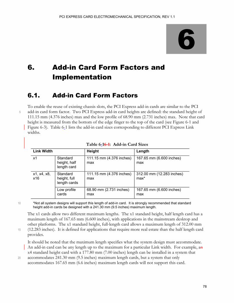
PCI EXPRESS CARD ELECTROMECHANICAL SPECIFICATION, REV 1.1
78
6. Add-in Card Form Factors and Implementation
6.1. Add-in Card Form Factors To enable the reuse of existing chassis slots, the PCI Express add-in cards are similar to the PCI add-in card form factor. Two PCI Express add-in card heights are defined: the standard height of 5 111.15 mm (4.376 inches) max and the low profile of 68.90 mm (2.731 inches) max. Note that card height is measured from the bottom of the edge finger to the top of the card (see Figure 6-1 and Figure 6-3). Table 6-1 lists the add-in card sizes corresponding to different PCI Express Link widths.
Table 6-16-1: Add-in Card Sizes
Link Width Height Length
x1 Standard height, half length card
111.15 mm (4.376 inches) max
167.65 mm (6.600 inches) max
Standard height, full length cards
111.15 mm (4.376 inches) max
312.00 mm (12.283 inches) max*
x1, x4, x8, x16
Low profile cards
68.90 mm (2.731 inches) max
167.65 mm (6.600 inches) max
*Not all system designs will support this length of add-in card. It is strongly recommended that standard 10 height add-in cards be designed with a 241.30 mm (9.5 inches) maximum length.
The x1 cards allow two different maximum lengths. The x1 standard height, half length card has a maximum length of 167.65 mm (6.600 inches), with applications in the mainstream desktop and other platforms. The x1 standard height, full-length card allows a maximum length of 312.00 mm (12.283 inches). It is defined for applications that require more real estate than the half length card 15 provides.
It should be noted that the maximum length specifies what the system design must accommodate. An add-in card can be any length up to the maximum for a particular Link width. For example, an x4 standard height card with a 177.80 mm (7.00 inches) length can be installed in a system that accommodates 241.30 mm (9.5 inches) maximum length cards, but a system that only 20 accommodates 167.65 mm (6.6 inches) maximum length cards will not support this card.
6

PCI EXPRESS CARD ELECTROMECHANICAL SPECIFICATION, REV 1.1
79
Figure 6-1 and Figure 6-3 show the standard PCI Express card form factor without and with the I/O bracket, respectively.
Figure 6-16-1: Standard Height PCI Express Add-in Card without the I/O Bracket

PCI EXPRESS CARD ELECTROMECHANICAL SPECIFICATION, REV 1.1
80
Figure 6-36-2: Standard Height PCI Express Add-in Card with the I/O Bracket and Card
Retainer
The mounting holes illustrated in Figure 6-1 are required only on the right end of the full-length card (312.00 mm). Those holes are needed to install the optional PCI add-in card retainer, as illustrated in Figure 6-3.
The mounting holes and keep-out zones around them marked as note 3 in Figure 6-1 are required on those cards in which the I/O bracket is mounted to the card directly. The purpose of this keep-5 out is to ensure that the card cannot short out on the I/O bracket. On full-length cards, a keep-out of 5.08 mm is required to prevent card components from being damaged by the system’s card guides (refer to Figure 6-1).
All graphics cards are required to be retention ready as defined in Section 5.2. This retention ready requirement may also apply to x1, x4, x8, or x16 I/O cards at each OEM, or add-in card 10 manufacturer’s discretion. See Section 5.2 for more information.
Special attention shall be given to graphics cards because of their potential high mass, driven by the high power allowed. This specification defines the additional feature and keepouts for x16 graphics cards for card retention shown in Figure 6-5.
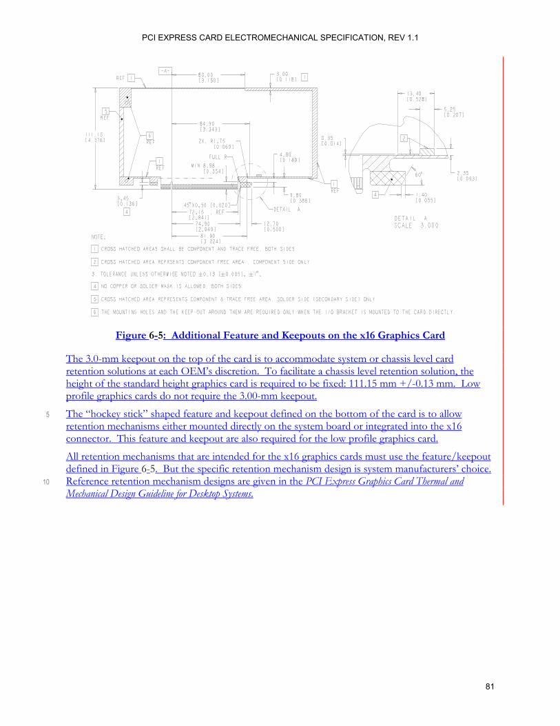
PCI EXPRESS CARD ELECTROMECHANICAL SPECIFICATION, REV 1.1
81
Figure 6-5: Additional Feature and Keepouts on the x16 Graphics Card
The 3.0-mm keepout on the top of the card is to accommodate system or chassis level card retention solutions at each OEM’s discretion. To facilitate a chassis level retention solution, the height of the standard height graphics card is required to be fixed: 111.15 mm +/-0.13 mm. Low profile graphics cards do not require the 3.00-mm keepout.
The “hockey stick” shaped feature and keepout defined on the bottom of the card is to allow 5 retention mechanisms either mounted directly on the system board or integrated into the x16 connector. This feature and keepout are also required for the low profile graphics card.
All retention mechanisms that are intended for the x16 graphics cards must use the feature/keepout defined in Figure 6-5. But the specific retention mechanism design is system manufacturers’ choice. Reference retention mechanism designs are given in the PCI Express Graphics Card Thermal and 10 Mechanical Design Guideline for Desktop Systems.
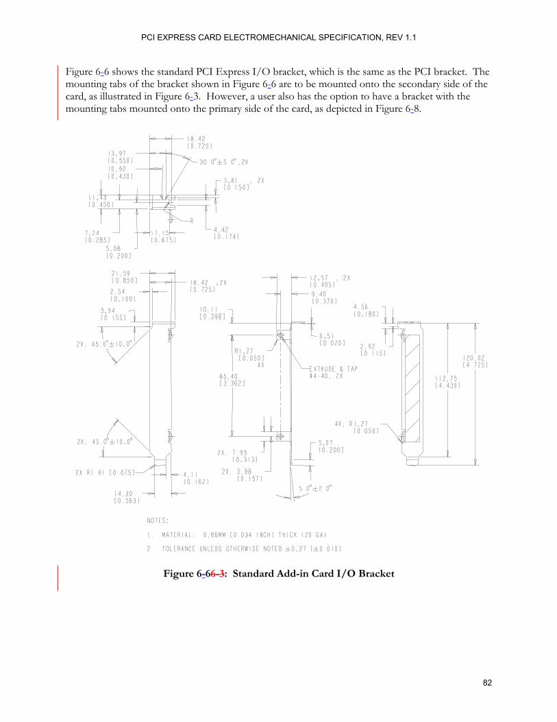
PCI EXPRESS CARD ELECTROMECHANICAL SPECIFICATION, REV 1.1
82
Figure 6-6 shows the standard PCI Express I/O bracket, which is the same as the PCI bracket. The mounting tabs of the bracket shown in Figure 6-6 are to be mounted onto the secondary side of the card, as illustrated in Figure 6-3. However, a user also has the option to have a bracket with the mounting tabs mounted onto the primary side of the card, as depicted in Figure 6-8.
Figure 6-66-3: Standard Add-in Card I/O Bracket
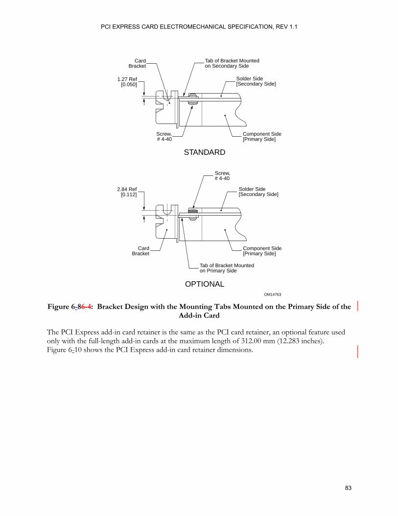
PCI EXPRESS CARD ELECTROMECHANICAL SPECIFICATION, REV 1.1
83
OM14763
Tab of Bracket Mountedon Secondary Side
CardBracket
CardBracket
Solder Side[Secondary Side]
Screw,# 4-40
Component Side[Primary Side]
STANDARD
OPTIONAL
2.84 Ref[0.112]
Screw,# 4-40
Solder Side[Secondary Side]
Component Side[Primary Side]
Tab of Bracket Mountedon Primary Side
1.27 Ref[0.050]
Figure 6-86-4: Bracket Design with the Mounting Tabs Mounted on the Primary Side of the Add-in Card
The PCI Express add-in card retainer is the same as the PCI card retainer, an optional feature used only with the full-length add-in cards at the maximum length of 312.00 mm (12.283 inches). Figure 6-10 shows the PCI Express add-in card retainer dimensions.
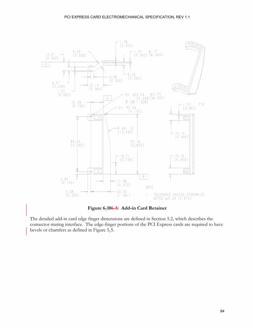
PCI EXPRESS CARD ELECTROMECHANICAL SPECIFICATION, REV 1.1
84
Figure 6-106-5: Add-in Card Retainer
The detailed add-in card edge finger dimensions are defined in Section 5.2, which describes the connector mating interface. The edge-finger portions of the PCI Express cards are required to have bevels or chamfers as defined in Figure 5-5.
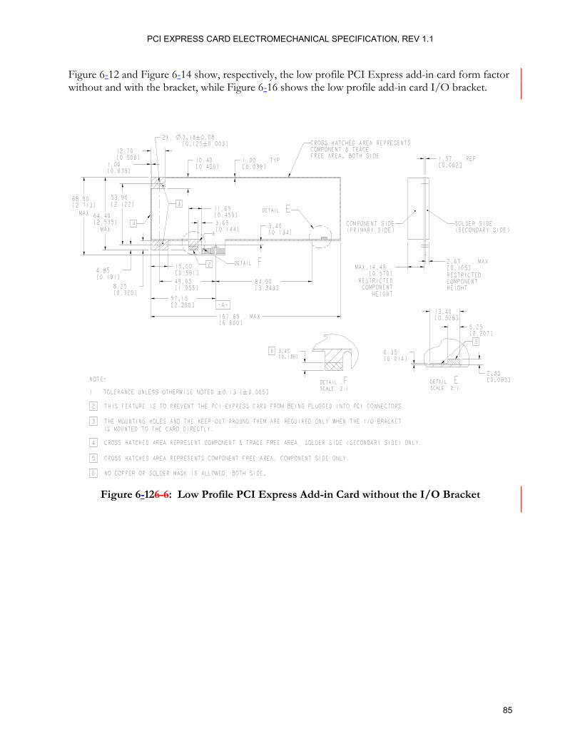
PCI EXPRESS CARD ELECTROMECHANICAL SPECIFICATION, REV 1.1
85
Figure 6-12 and Figure 6-14 show, respectively, the low profile PCI Express add-in card form factor without and with the bracket, while Figure 6-16 shows the low profile add-in card I/O bracket.
Figure 6-126-6: Low Profile PCI Express Add-in Card without the I/O Bracket
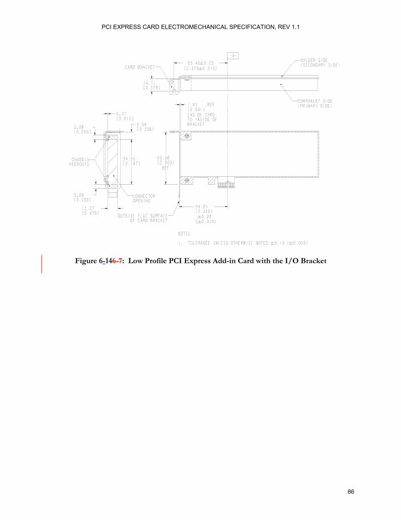
PCI EXPRESS CARD ELECTROMECHANICAL SPECIFICATION, REV 1.1
86
Figure 6-146-7: Low Profile PCI Express Add-in Card with the I/O Bracket

PCI EXPRESS CARD ELECTROMECHANICAL SPECIFICATION, REV 1.1
87
Figure 6-166-8: Low Profile I/O Bracket
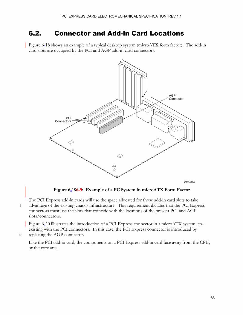
PCI EXPRESS CARD ELECTROMECHANICAL SPECIFICATION, REV 1.1
88
6.2. Connector and Add-in Card Locations Figure 6-18 shows an example of a typical desktop system (microATX form factor). The add-in card slots are occupied by the PCI and AGP add-in card connectors.
PCIConnectors
OM14764
AGPConnector
Figure 6-186-9: Example of a PC System in microATX Form Factor
The PCI Express add-in cards will use the space allocated for those add-in card slots to take advantage of the existing chassis infrastructure. This requirement dictates that the PCI Express 5 connectors must use the slots that coincide with the locations of the present PCI and AGP slots/connectors.
Figure 6-20 illustrates the introduction of a PCI Express connector in a microATX system, co-existing with the PCI connectors. In this case, the PCI Express connector is introduced by replacing the AGP connector. 10
Like the PCI add-in card, the components on a PCI Express add-in card face away from the CPU, or the core area.
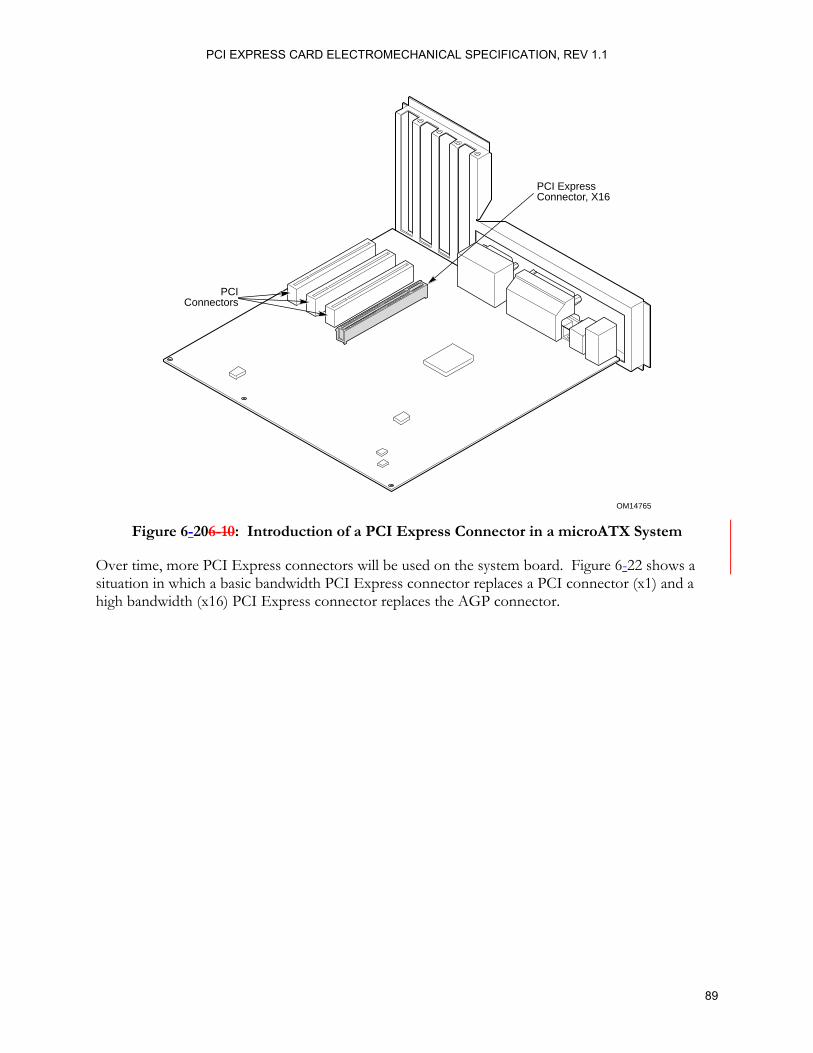
PCI EXPRESS CARD ELECTROMECHANICAL SPECIFICATION, REV 1.1
89
PCIConnectors
OM14765
PCI ExpressConnector, X16
Figure 6-206-10: Introduction of a PCI Express Connector in a microATX System
Over time, more PCI Express connectors will be used on the system board. Figure 6-22 shows a situation in which a basic bandwidth PCI Express connector replaces a PCI connector (x1) and a high bandwidth (x16) PCI Express connector replaces the AGP connector.
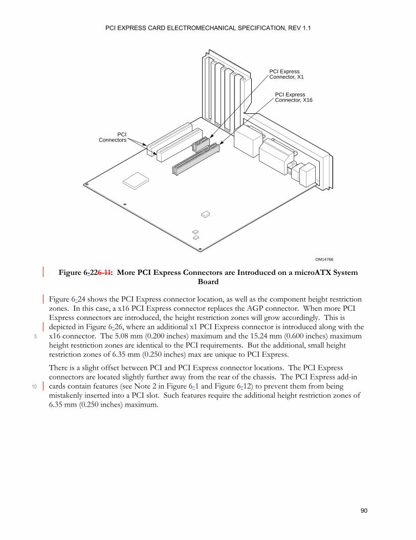
PCI EXPRESS CARD ELECTROMECHANICAL SPECIFICATION, REV 1.1
90
PCIConnectors
OM14766
PCI ExpressConnector, X1
PCI ExpressConnector, X16
Figure 6-226-11: More PCI Express Connectors are Introduced on a microATX System
Board
Figure 6-24 shows the PCI Express connector location, as well as the component height restriction zones. In this case, a x16 PCI Express connector replaces the AGP connector. When more PCI Express connectors are introduced, the height restriction zones will grow accordingly. This is depicted in Figure 6-26, where an additional x1 PCI Express connector is introduced along with the x16 connector. The 5.08 mm (0.200 inches) maximum and the 15.24 mm (0.600 inches) maximum 5 height restriction zones are identical to the PCI requirements. But the additional, small height restriction zones of 6.35 mm (0.250 inches) max are unique to PCI Express.
There is a slight offset between PCI and PCI Express connector locations. The PCI Express connectors are located slightly further away from the rear of the chassis. The PCI Express add-in cards contain features (see Note 2 in Figure 6-1 and Figure 6-12) to prevent them from being 10 mistakenly inserted into a PCI slot. Such features require the additional height restriction zones of 6.35 mm (0.250 inches) maximum.
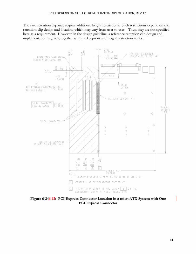
PCI EXPRESS CARD ELECTROMECHANICAL SPECIFICATION, REV 1.1
91
The card retention clip may require additional height restrictions. Such restrictions depend on the retention clip design and location, which may vary from user to user. Thus, they are not specified here as a requirement. However, in the design guideline, a reference retention clip design and implementation is given, together with the keep-out and height restriction zones.
Figure 6-246-12: PCI Express Connector Location in a microATX System with One
PCI Express Connector
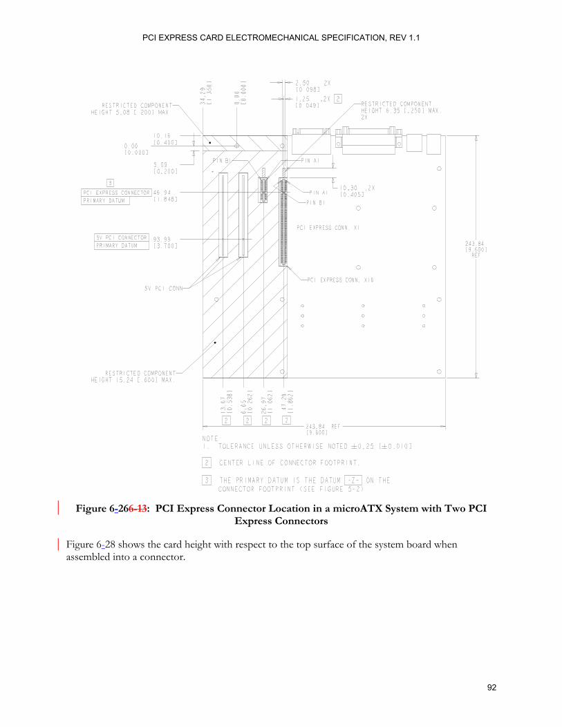
PCI EXPRESS CARD ELECTROMECHANICAL SPECIFICATION, REV 1.1
92
Figure 6-266-13: PCI Express Connector Location in a microATX System with Two PCI
Express Connectors
Figure 6-28 shows the card height with respect to the top surface of the system board when assembled into a connector.
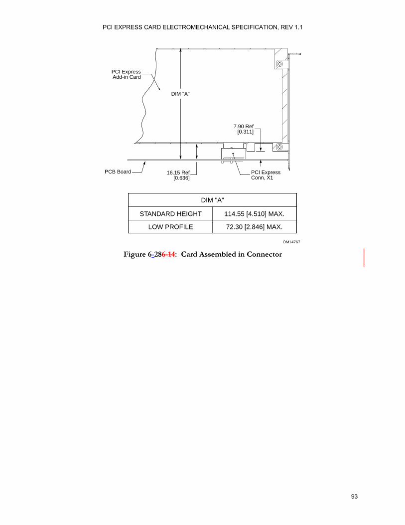
PCI EXPRESS CARD ELECTROMECHANICAL SPECIFICATION, REV 1.1
93
OM14767
PCB Board
PCI ExpressAdd-in Card
PCI ExpressConn, X1
16.15 Ref[0.636]
7.90 Ref[0.311]
DIM "A"
STANDARD HEIGHT
LOW PROFILE
114.55 [4.510] MAX.
72.30 [2.846] MAX.
DIM "A"
Figure 6-286-14: Card Assembled in Connector
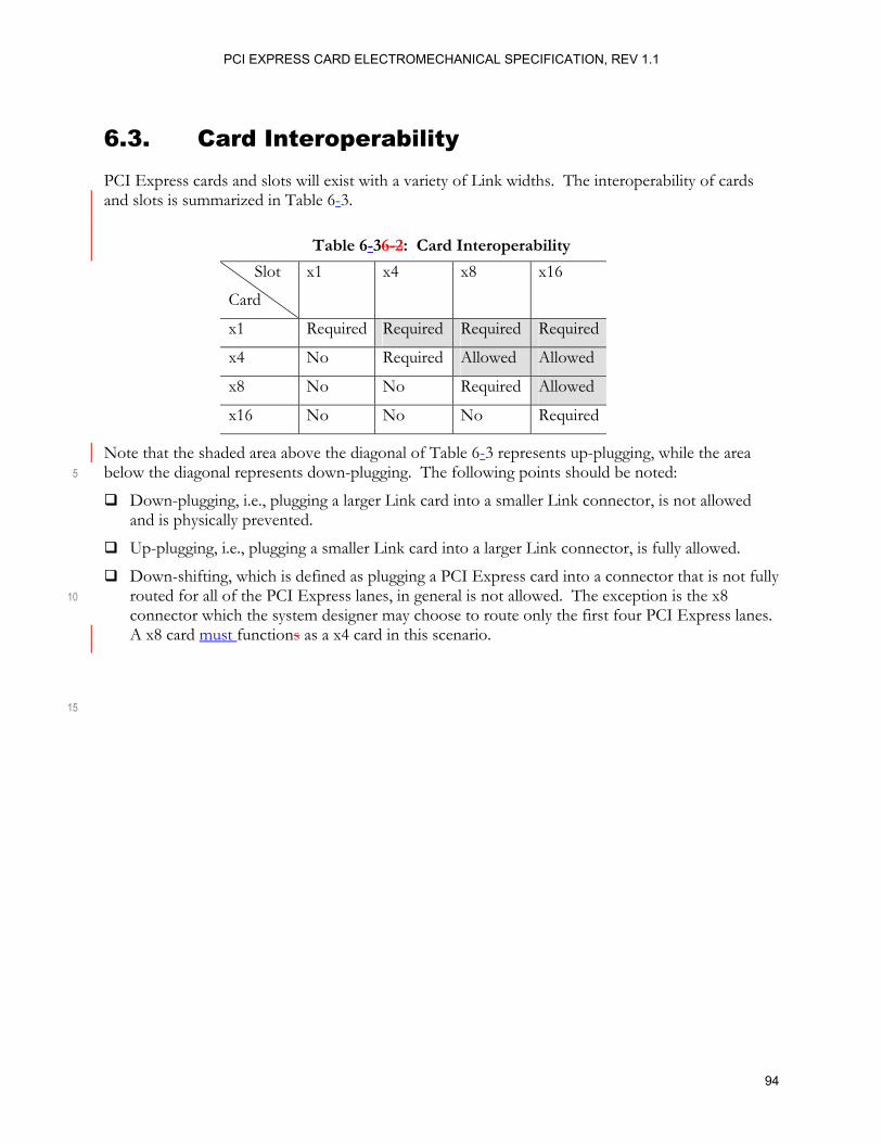
PCI EXPRESS CARD ELECTROMECHANICAL SPECIFICATION, REV 1.1
94
6.3. Card Interoperability PCI Express cards and slots will exist with a variety of Link widths. The interoperability of cards and slots is summarized in Table 6-3.
Table 6-36-2: Card Interoperability
Slot
Card
x1 x4 x8 x16
x1 Required Required Required Required
x4 No Required Allowed Allowed
x8 No No Required Allowed
x16 No No No Required Note that the shaded area above the diagonal of Table 6-3 represents up-plugging, while the area below the diagonal represents down-plugging. The following points should be noted: 5
Down-plugging, i.e., plugging a larger Link card into a smaller Link connector, is not allowed and is physically prevented.
Up-plugging, i.e., plugging a smaller Link card into a larger Link connector, is fully allowed.
Down-shifting, which is defined as plugging a PCI Express card into a connector that is not fully routed for all of the PCI Express lanes, in general is not allowed. The exception is the x8 10 connector which the system designer may choose to route only the first four PCI Express lanes. A x8 card must functions as a x4 card in this scenario.
15

PCI EXPRESS CARD ELECTROMECHANICAL SPECIFICATION, REV 1.1
95

PCI EXPRESS CARD ELECTROMECHANICAL SPECIFICATION, REV 1.1
96
Acknowledgements
The following persons were instrumental in the development of the PCI Express Card Electromechanical Specification:1
Richard Allirot Hewlett-Packard Company Dave Moss Dell Computer Corporation Bob Atkinson Tyco International, Ltd. Scott Noble Intel Corporation Ed Boeckmann 3Dlabs, Inc. Ltd. Ta-Wee Ong Molex Incorporated Jim Brewer Dell Computer Corporation John Pescatore Dell Computer Corporation James Bullington 3Dlabs, Inc. Ltd. Curt Progl Dell Computer Corporation Raymond Chin Hewlett-Packard Company Eddie Reid Intel Corporation Michael Cheong Molex Incorporated Martha Rupert FCI KengYin Chok Molex Incorporated Rodrigo Samper IBM Corporation Dr. Jason Chou Foxconn Electronics, Inc. Bill Sauber Dell Computer Corporation Don Craven Intel Corporation Rick Schuckle Dell Computer Corporation Dave Davitian Tyco International, Ltd. Joe Sekel Dell Computer Corporation Bassam Elkhoury Intel Corporation Joanne E. Shipe Foxconn Electronics, Inc. Ikuo Enomoto Tyco International, Ltd. Dave Sideck FCI David Farmer 3Dlabs, Inc. Ltd. Chuck Stancil Hewlett-Packard Company Don Faw Intel Corporation John Stuewe Dell Computer Corporation George Hayek Intel Corporation Tom Sultzer FCI Dave Helster Tyco International, Ltd. Toru Tamaki Tyco International, Ltd. Ted Holden Intel Corporation Junichi Tanigawa Tyco International, Ltd. Carl Jackson Hewlett-Packard Company Clay Terry 3Dlabs, Inc. Ltd. Mike Krause Hewlett-Packard Company SY Theng Molex Incorporated Doron Lapidot Tyco International, Ltd. Alok Tripathi Intel Corporation Cliff Lee Intel Corporation Andy Vasbinder FCI PT Lim Molex Incorporated Gary Verdun Dell Computer Corporation Yun Ling Intel Corporation Andy Volk Intel Corporation Howard Locker IBM Corporation Chris Womack Hewlett-Packard Company Alan MacDougall Molex Incorporated Mike Woren Tyco International, Ltd. Bob Marshall FCI Yoshisha Yamamoto Tyco International, Ltd. Mike Miller IBM Corporation Dave Zenz Dell Computer Corporation
5
1 Company affiliation listed is at the time of specification contributions.