PCCtest 27x/37x Technical Reference Manual 27x/37x Technical Reference Manual M200009-01 February...
27
PCCtest 27x/37x Technical Reference Manual M200009-01 February 1996 Preliminary Sycard Technology 1180-F Miraloma Way Sunnyvale, CA 94086 (408) 749-0130 (408) 749-1323 FAX
-
Upload
hoangtuong -
Category
Documents
-
view
218 -
download
0
Transcript of PCCtest 27x/37x Technical Reference Manual 27x/37x Technical Reference Manual M200009-01 February...
PCCtest 27x/37xTechnical Reference
Manual
M200009-01February 1996
Preliminary
Sycard Technology1180-F Miraloma WaySunnyvale, CA 94086(408) 749-0130(408) 749-1323 FAX

PCCtest 27x/37x Technical Reference Manual Page 1
M200009-01 1994-96 Sycard Technology
1. Introduction
The PCCtest PCMCIA tester is designed to provide manufacturers of PCMCIA based hosts a quick method of testingand verifying the operation of the PC Card sockets.
The PCCtest is Type II PC Card that plugs into a standard PCMCIA Type II or III socket. The board is designed forboth automated GO/NO-GO testing and component level debug. Software resides on both the host PC and PCCtestunit.
An on board microcontroller provides the intelligence for the PCCtest unit. The microcontroller is responsible forverifying I/O signals and also provides test stimulus to the PC card socket. The microcontroller can determine thetype of error and can even narrow the error down to a specific pin or group of pins.
The PCCtest contains an on-board A/D to provide accurate measurement of VCC and VPP voltages. A digital audiotest provides a standard 1KHz tone to test the audio function when the PC card is configured for I/O mode.
Sycard Technology provides a DOS application to test Intel 82365SL compatible socket controllers. Simplecommand line invocation, allows tests to be embedded into batch test files. OEMs that wish to use the PCCtest on anon-DOS platform can use this specification to develop custom test applications. Sycard can also provide a sourcelicense for the DOS test application.
The PCCtest unit operates in two different modes:
Standalone mode - All communications to test hardware occurs through the PC card interface.
Serial Debug Mode - Accesses by host system displayed on remote serial terminal.
Which mode of use depends on the type of testing or debugging desired. The serial debug mode is only availablewith the PCCtest 350 unit.
2.0 Architecture of the PCCtest
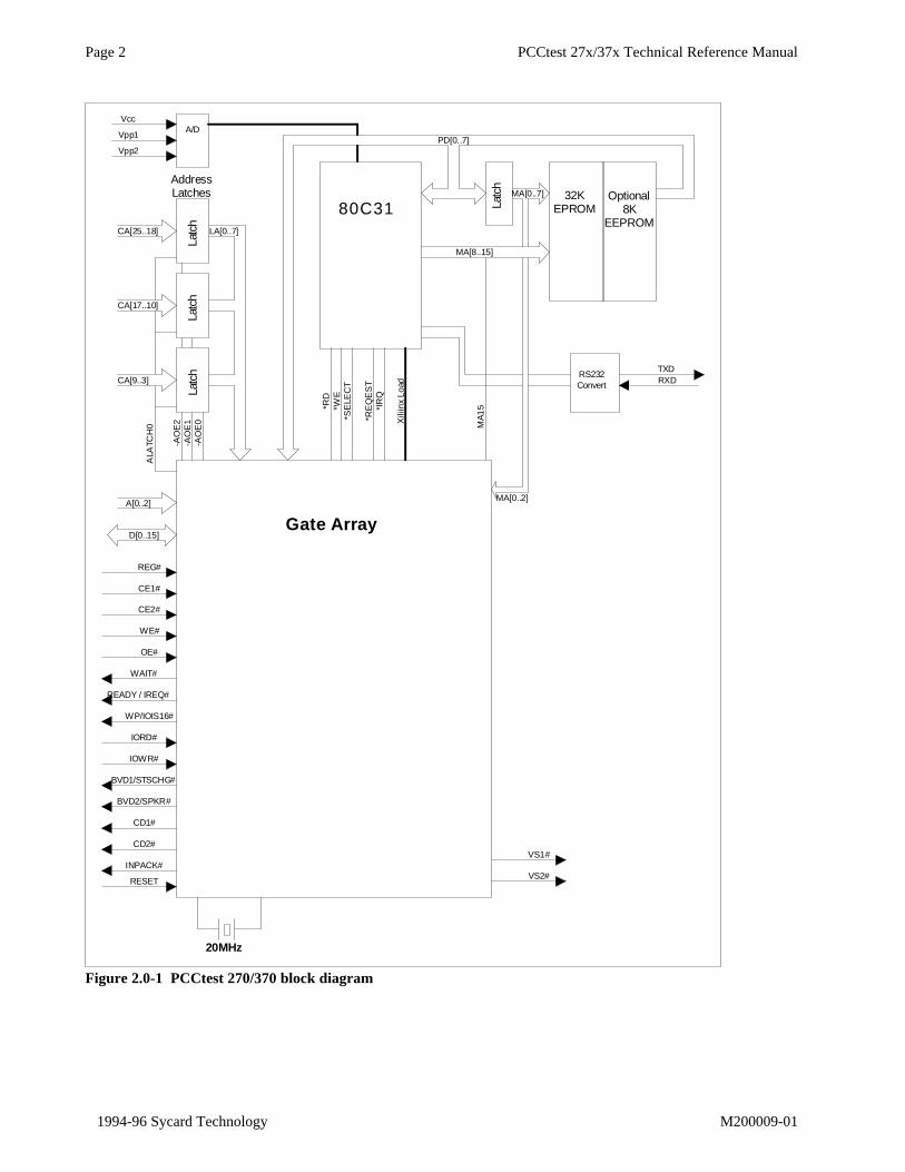
Figure 2.0-1 Illustrates the architecture of the PCCtest model 270/370. The functional blocks can be partitioned in tothe following major sub-sections:
• Tester Gate Array (TGA) and Address Latches• Microcontroller• A/D Converter and Logic
All interface to the PCCtest unit is via eight registers contained in the TGA. These eight registers control the varioustest functions contained within the PCCtest unit. These registers can be accessed through the PC Card interface orthrough the on-board serial port. There are two major types of tests performed by the PCCtest unit - thoseimplemented by the Test Gate Array (TGA) and microprocessor assisted tests. The TGA based tests are designed totest the basic functionality of the interface. These tests will verify the basic operation of the interface includingaccess strobes, data bus and address bus. Once these basic access modes are verified, the microprocessor assistedtests are run to verify the remainder of the interface.
The microprocessor assisted tests are designed to test areas of the interface that are difficult to test through a “dumb”interface. These tests include voltage measurements, card detect tests and Direct Memory Access (DMA) tests.Microprocessor assisted tests are controlled through the TGA registers.
Page 2 PCCtest 27x/37x Technical Reference Manual
1994-96 Sycard Technology M200009-01
REG#
OE#
WE#
CE1#
CE2#
WAIT#
IORD#
IOWR#
CD1#
CD2#
BVD1/STSCHG#
BVD2/SPKR#
READY / IREQ#
WP/IOIS16#
D[0..15]
80C3132K
EPROMOptional
8KEEPROM
Latc
h
Latc
hLa
tch
Latc
hAddressLatches
MA[0..2]
MA[8..15]
PD[0..7]
MA[0..7]
LA[0..7]
-AO
E2
-AO
E1
-AO
E0
ALA
TCH
0 MA1
5*WE
*RD
*SE
LEC
T
*RE
QE
ST
CA[25..18]
CA[17..10]
CA[9..3]*I
RQ
A[0..2]
RS232Convert
TXDRXD
A/DVcc
Vpp1
Xili
inx
Load
Gate Array
20MHz
INPACK#
Vpp2
RESET VS2#
VS1#
Figure 2.0-1 PCCtest 270/370 block diagram
PCCtest 27x/37x Technical Reference Manual Page 3
M200009-01 1994-96 Sycard Technology
3.0 Tests Using the Test Gate Array
Most of the basic interface tests are handled in the TGA. Eight registers control the operation of the TGA. AppendixA lists the status and control registers contained in the TGA. Note that all write registers cannot be read back. It isup to the programmer to maintain an image of the write registers, since a read/modify/write operation is not possiblefor some of the register bits.
3.1 Initializing the PCCtest
The PCCtest must be powered through the host socket before any test operations can begin. The PCCtest model250/260/350/360 must be powered to 5v Vcc. PCCtest models 270/370/273/373 can be powered to 3.3 or 5.0V. AllPCCtest units requires a power-on reset to initialize the internal operating circuitry. Care must be taken whenswitching operating voltages on the PCCtest 270/370/273/373. Do not switch from 3.3V to 5.0V or 5.0V to 3.3Vwithout allowing the power to go to first go to 0V.
Note: Vpp1 and Vpp2 can be measured by the PCCtest, but are not required for PCCtest operation.
Note: The Card Detect (CD1# and CD2#) signals on PCCtest models 250/350/260/360/270/370 areimplemented as CMOS outputs. When the PCCtest is powered down, there is no low impedance path toground. Depending on the pull-up values on the CD1# and CD2# signals, there may not be a low on thesesignals when the socket is powered down. There are some socket controllers that require the card detects beactive (low) before power can be applied to the socket.
Note: Host socket implementations that use Card Detects to enable power to the socket are not compatiblewith the PCCtest 250/350/260/360/270/370. This type of implementation is typically used in single chipimplementation such as the Vadem VG-230, VG-469, Chips and Technology F8680 and the AMD Elan.Sycard supplies a version of the PCCtest, called the model 230/330/273/373, for these type ofimplementations. The PCCtest models 230, 330, 273 and 373 internally ground card detects (CD1# andCD2#.)
On power-up, the PCCtest's microcontroller initializes itself and loads the configuration into the TGA. The PCCtestcontains its own power-on reset circuitry and ignores the PCMCIA interface RESET signal. During this power-upphase all I/O signals are tri-stated. Once the microcontroller completes its initialization the following signal areforced low:
CD1# (PCCtest models 250/350/260/360/270/370 only)CD2# (PCCtest models 250/350/260/360/270/370 only)WP#
3.2 Opening a Memory and I/O Window to the PCCtest
In order to access the test resources in the PCCtest, a 16 bit memory and an 8 bit I/O window must be opened to thePCCtest. Both a I/O and memory window are required to fully test the PC Card interface. The PCCtest containseight 8-bit I/O mapped registers. An I/O window of at least eight bytes is required to access all the PCCtest'sregisters.
Note: For information on opening an I/O window, consult your socket controller chip user's manual.
Note: The PCCtest is not able operate in a memory only interface.
A memory window with a length of at least 1 word is require to test the interface's memory interface. Most socketcontrollers provide a minimum window length of 4K bytes.

Page 4 PCCtest 27x/37x Technical Reference Manual
1994-96 Sycard Technology M200009-01
PCCtest 27x/37x Technical Reference Manual Page 5
M200009-01 1994-96 Sycard Technology
3.3 Preliminary Tests
Before accessing the PCCtest hardware, the test software should verify the basic operation of the socket controllerand that the PCCtest is properly inserted into the socket. This will avoid any unnecessary delays or erroneous errormessages. The following sequence is used in Sycard's PCCtest software:
1. Verify socket controller is present by executing a simple register test.2. Power-up socket.3. Wait 1 second for PCCtest to initialize.4. Verify card detects are active (CD1# and CD2# are low)
If any of these tests fail, further testing is not possible.
3.4 Basic Tests
Once the socket controller has been verified and card detects are active, the PCCtest’s registers can be accessed. Thispart of the test procedure verifies the basic read/write operation of the card. If any failures are detected in the basictest, more advanced tests may return erroneous results.
a. Basic 8 bit read/write to the LTHL register - Verify basic 8 bit I/O read.
b. Basic 16 bit read/write to the LTHL/LTHH register - Verify basic 16 bit I/O read.
c. Basic 16 bit read/write to memory - Memory
Once these tests pass, further more detailed tests can be run.
Note: Basic 8 bit operation of the PCCtest requires the following signals to be working:
D[7:0]IORD#IOWR#CE1#A[2:0]
3.5 Data Tests
The PC Card data bus may be tested through several methods. For a standalone test, the host writes data to the datalatches LTHL at I/O offset 00H or LTHH at 01H. Both 8 and 16 bit I/O accesses are allowed. Data is latched intothese registers on an I/O write to the LTHL and LTHH registers. Once data is written, it can be read back to verifythat all data bits that have been written are correct.
Common and attribute memory data pattern tests can be accomplished by accessing the same LTHL and LTHHregisters. These registers are accessed on any common or attribute memory read or write, regardless of address. Onpower-on reset access to these registers through the memory space are disabled. To enable these registers set theDATA_ENB bit in the MBITS register at offset 07H.
Note: In revision 1.02 and earlier versions of the PCCtest hardware, access to the LTHL and LTHHregisters through common or attribute memory are always enabled. The PCCtest revision number is locatedon the serial number label.
PCCtest units with the serial interface may test the data bus by writing/reading from the LTHL and LTHH throughthe PC Card interface and reading/writing via the serial interface.

Page 6 PCCtest 27x/37x Technical Reference Manual
1994-96 Sycard Technology M200009-01
3.6 Address and REG# Tests
The PC Card’s 26 bit address bus can be tested by writing various address patterns to the PCCtest unit. All addressbits can be latched and read through the PC Card host interface or through the serial interface. The address latchingcircuit must be armed prior to the access that triggers the latching circuitry. Addresses are latched on the falling edgeof the control strobes, WE#, OE#, IORD#, or IOWR#.
Note: The latching signal is a logical OR of the OE#, WE#, IORD# and IOWR# strobes qualified by eitherCE1# or CE2#.
Arming of the address latches is accomplished through the ARM bit in PCCtest register 6. A low to high transition ofthis bit will arm the latch. Any access after this arm will result in the latching of all 26 address signals on theinterface. The following C code is used to arm the address latch:
reg_data = inportb(tester_addr+6); outportb(tester_addr+6,reg_data & 0xbf); outportb(tester_addr+6,reg_data | 0x40);
The latched values of A[2:0], REG#, CE1# and CE2# signals can be read directly from the LOW_LATCH register atoffset 03h. The other address bits are read, by first selecting the appropriate address latch and then reading the valuefrom the LADD register at offset 03h.
ASEL[1:0] Contents of LADD register01 A[10:3]10 A[18:11]11 A[25:19]
Table 3.6-1 Address Latch Select Values
The following procedure is used to latch the address and read the data from the address latches to create a 26 bitaddress.
1. Clear the ARM bit in MISC register at offset 06h.2. Set the ARM bit in the MISC register. The address latch is now armed.3. Access the card with IORD#, IOWR#, OE# or WE# strobe. The address of the access is latched on the
falling edge of the strobe.4. Read the lower 3 bits A[2:0] from the LOW_LATCH register at offset 03h.5. Select the A[10:3] latch by setting ASEL[1:0] to 01 in the MISC register at offset 06h.6. Read the contents of the A[10:3] latch from the LADD register at offset 02h.7. Select the A[18:11] latch by setting the ASEL[1:0] to 10 in the MISC register at offset 06h.8. Read the contents of the A[18:11] latch from the LADD register at offset 02h.9. Select the A[25:19] latch by setting the ASEL[1:0] to 11 in the MISC register at offset 06h.10. Read the contents of the A[25:19] latch from the LADD register at offset 02h.
PCCtest units with the serial interface may test the address bus by reading the address registers via serial commands.This allows the user to debug the address bus when the data bus does not work well enough to read the addressregisters through the PC Card interface.
3.7 Timing Measurements
The PCCtest provides a flexible timing measurement circuit providing 50ns resolution. This circuit can measure fromthe rising/falling edge of any of the control strobes to the rising falling edge of the same set of signals. The followingtable lists the various control strobes that can be measured:

PCCtest 27x/37x Technical Reference Manual Page 7
M200009-01 1994-96 Sycard Technology
Signal Description TCR ValueOE# Memory Read Strobe 3BhWE# Memory Write Strobe 2AhIORD# I/O Read Strobe 08hIOWR# I/O Write Strobe 19hCE1# Chip Enable 1 4ChCE2# Chip Enable 2 5Dh
Table 3.7-1 Common Strobe Measurements TCR Values
The signal and polarity that start the timer is selected via the STR[2:0] and the STRPOL bits in the TCR register. TheSTP[2:0] and STPPOL bits determine the signal that stops the timer. The following examples illustrate the valuesprogrammed into the TCR register (offset 05h) for various timing measurements:
Timing Measurement TCR ValueFalling edge of CE1# to rising edge of OE# 3ChPulse width of IORD# 08hPulse width of IOWR# 19hRising edge of CE1# to rising edge of OE# 34hPulse width of WE# 2Ah
Table 3.7-2 Various Strobe Measurements TCR Values
As with the address latching circuit, the timing logic is armed and the next access to the card is measured. The timingmeasurement is armed through an I/O write to the TRST register at offset 02h. Once armed, the timer will start onfirst instance of the value programmed into the STR[2:0] register. The value can be read from the TIM register atoffset 04h. The value read from the TIM register is multiplied by the sample rate (50ns) to obtain the strobe width.
3.8 Testing RESET
The RESET signal is an input to the PCCtest unit. RESET is only monitored by the PCCtest and will not reset thePCCtest or cause any other state change. The state of the RESET bit can be read from bit 7 of the LOW_LATCHregister at offset 03h.
3.9 INPACK# Tests
PCCtest can generate INPACK# on all I/O reads. Most socket controllers can use INPACK# to gate the PC Card dataon to the host system data bus. Setting the INPACK_EN bit in the MISC control register at offset 05h enablesINPACK# generation on all I/O reads.
3.10 Testing WAIT#
A programmable wait state generator is used to generate wait states to simulate slow I/O or memory devices. Thewait state generator is capable of generating wait states up to 3160ns (700ns in Rev 1.02 firmware). This covers thefull range of PC card access times. Used in conjunction with the pulse measuring circuits, can result in accuratemeasurement of read/write strobes widths. Timing for the wait state generator is based on the PCCtest’s main crystal(20Mhz).
Page 8 PCCtest 27x/37x Technical Reference Manual
1994-96 Sycard Technology M200009-01
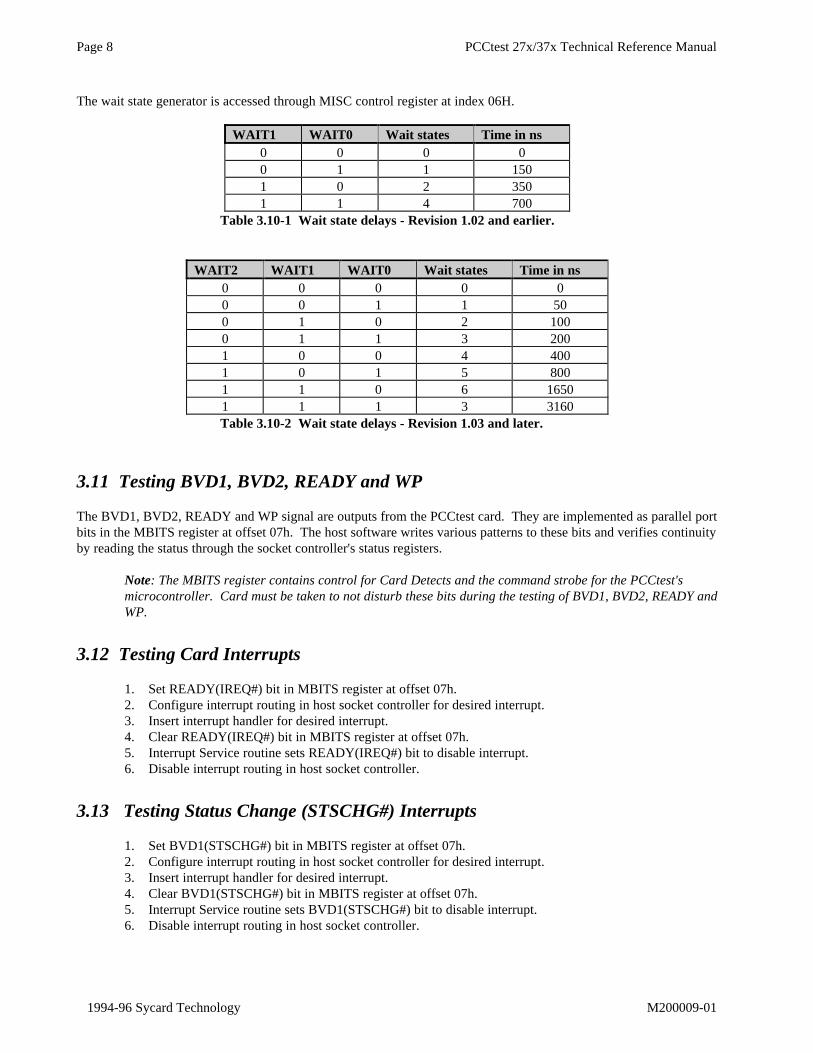
The wait state generator is accessed through MISC control register at index 06H.
WAIT1 WAIT0 Wait states Time in ns0 0 0 00 1 1 1501 0 2 3501 1 4 700
Table 3.10-1 Wait state delays - Revision 1.02 and earlier.
WAIT2 WAIT1 WAIT0 Wait states Time in ns0 0 0 0 00 0 1 1 500 1 0 2 1000 1 1 3 2001 0 0 4 4001 0 1 5 8001 1 0 6 16501 1 1 3 3160Table 3.10-2 Wait state delays - Revision 1.03 and later.
3.11 Testing BVD1, BVD2, READY and WP
The BVD1, BVD2, READY and WP signal are outputs from the PCCtest card. They are implemented as parallel portbits in the MBITS register at offset 07h. The host software writes various patterns to these bits and verifies continuityby reading the status through the socket controller's status registers.
Note: The MBITS register contains control for Card Detects and the command strobe for the PCCtest'smicrocontroller. Card must be taken to not disturb these bits during the testing of BVD1, BVD2, READY andWP.
3.12 Testing Card Interrupts
1. Set READY(IREQ#) bit in MBITS register at offset 07h.2. Configure interrupt routing in host socket controller for desired interrupt.3. Insert interrupt handler for desired interrupt.4. Clear READY(IREQ#) bit in MBITS register at offset 07h.5. Interrupt Service routine sets READY(IREQ#) bit to disable interrupt.6. Disable interrupt routing in host socket controller.
3.13 Testing Status Change (STSCHG#) Interrupts
1. Set BVD1(STSCHG#) bit in MBITS register at offset 07h.2. Configure interrupt routing in host socket controller for desired interrupt.3. Insert interrupt handler for desired interrupt.4. Clear BVD1(STSCHG#) bit in MBITS register at offset 07h.5. Interrupt Service routine sets BVD1(STSCHG#) bit to disable interrupt.6. Disable interrupt routing in host socket controller.

PCCtest 27x/37x Technical Reference Manual Page 9
M200009-01 1994-96 Sycard Technology
3.14 Testing Voltage Sense (VS1# and VS2#)
The PCCtest models 270/370/273/373 support testing of the VS1# and VS2# signals. On card initialization, VS1#and VS2# are both set inactive (high). VS1# and VS2# can be independently forced active (low) through the TCRregister at offset 5. VS1# can be forced active (low) by setting STR[2:0] equal to 111. VS2# can be forced active(low) by setting STP[2:0] to 111.
4.0 Microprocessor Assisted Tests
The on-board microcontroller assists in certain tests that cannot be easily implemented through the register basedinterface. The microcontroller accept commands via the PCCtest's low and high data registers and executes oncommand from the host. Status of the requested operation may be returned in the PCCtest’s LTHH and LTHLregisters.
4.1 Microprocessor Command Interface
Commands and command parameters are loaded in the LTHL and LTHH registers. After the host writes the testcommand into these registers, it requests the PCCtest microprocessor to execute the command by strobing theMPU_REQ bit in MBITs register. A low to high pulse is required to initiate the command. The minimum pulsewidth for the microcontroller to accept the command is 3 microseconds. When the microcontroller receives the startstrobe it will clear the READY signal. On completion of the command it will set READY. Commands that returnvalues will return them in LTLL and LTHLregisters.
There are over 20 commands in the PCCtest 250/350 and more in advanced models.
Note: Commands can be written into the PCCtest LTHL and LTHH register with an I/O or memory writecommand. Commands that require a value be placed into the LTHH register, must be written using a 16 bitmemory write command. It is not possible to do an 8 bit I/O write to the LTHL register.
All commands listed in this section follow the same command procedure as described above.
4.2 Voltage Measurements
The PCCtest's A/D converter has an 8 resolution and is controlled by the on-board microcontroller. An analogmultiplexer can select between Vcc, Vpp1, Vpp2 and the RESET signal. Data conversion and selection of the voltageto be measured is handled by the microcontroller. The following commands
Command ValueMeasure Vcc 10hMeasure Vpp1 11hMeasure Vpp2 12h
Table 4.2-1 A/D Command
a. Place desired voltage measurement command in LTHL registerb. Initiate measurement by setting MPU_REQ bit in MBITS register at offset 07h.c. Wait 2us and then clear MPU_REQ bit in MBITSd. Wait for READY to come truee. Read 8 bit value from LTHL registerf. Using the following formula(s) convert value into volts.

Page 10 PCCtest 27x/37x Technical Reference Manual
1994-96 Sycard Technology M200009-01
For Vpp1 and Vpp2
Vpp = value * 0.055
For Vcc
Vcc = value * 0.023
4.3 Card Detect Tests
Card detects are often difficult to test on the PC Card interface. Socket controllers typically tri-state the interfacewhen card detects are deasserted. The PCCtest handles this problem by using the on-board microcontroller tomomentarily deasserting card detects. The host test software can verify the operation of the card detects bymonitoring the change the change in state. PCCtest can individually test each card detect (CD1# and CD2#).
To test CD1#
a. Place the CD1# strobe command (70h) into the LTHL registerb. The number of milliseconds to deassert CD1# is placed in the LTHH registerc. Toggle the MPU_REQ bit in the MBITS register from low to high and back to low for a minimum of
2us.d. The PCCtest's microcontroller will wait the number of milliseconds set in the LTHH register and pulse
the CD1# pin low for the same number of milliseconds.e. The host software can monitor the state of the CD1# signal through the host socket controllers status
register.
To test CD2#
Same procedure as above, but the CD2# strobe command is 71h.
4.4 Speaker (SPKR#) Testing
The SPEAKER command initiates a 500ms 1KHz square wave to be placed on the SPKR# signal. If the socketcontroller is properly programmed and configured to route the SPKR# signal to a speaker driver circuit, a tone can begenerated to verify the PC Card SPKR# signal. The command procedure is the same as the other microprocessorassisted commands. The command byte for the speaker test is 60h.
4.5 Identifying the PCCtest
Test software can identify the version of PCCtest hardware and firmware by requesting making a request via theLTHL register.
Test Command ByteRequest Model Number 43H
Request Major Revision Level 41HRequest Minor Revision Level 42H
Table 4.5-1 Misc commands
PCCtest 27x/37x Technical Reference Manual Page 11
M200009-01 1994-96 Sycard Technology
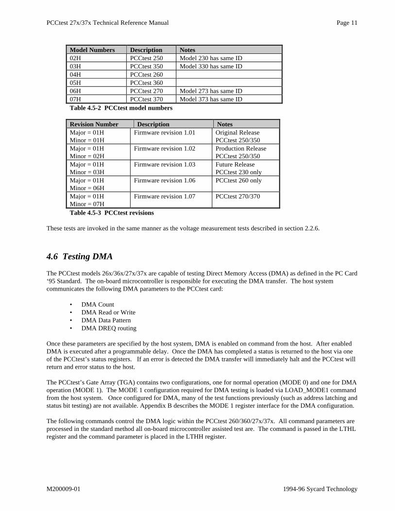
Model Numbers Description Notes02H PCCtest 250 Model 230 has same ID03H PCCtest 350 Model 330 has same ID04H PCCtest 26005H PCCtest 36006H PCCtest 270 Model 273 has same ID07H PCCtest 370 Model 373 has same IDTable 4.5-2 PCCtest model numbers
Revision Number Description NotesMajor = 01HMinor = 01H
Firmware revision 1.01 Original ReleasePCCtest 250/350
Major = 01HMinor = 02H
Firmware revision 1.02 Production ReleasePCCtest 250/350
Major = 01HMinor = 03H
Firmware revision 1.03 Future ReleasePCCtest 230 only
Major = 01HMinor = 06H
Firmware revision 1.06 PCCtest 260 only
Major = 01HMinor = 07H
Firmware revision 1.07 PCCtest 270/370
Table 4.5-3 PCCtest revisions
These tests are invoked in the same manner as the voltage measurement tests described in section 2.2.6.
4.6 Testing DMA
The PCCtest models 26x/36x/27x/37x are capable of testing Direct Memory Access (DMA) as defined in the PC Card‘95 Standard. The on-board microcontroller is responsible for executing the DMA transfer. The host systemcommunicates the following DMA parameters to the PCCtest card:
• DMA Count• DMA Read or Write• DMA Data Pattern• DMA DREQ routing
Once these parameters are specified by the host system, DMA is enabled on command from the host. After enabledDMA is executed after a programmable delay. Once the DMA has completed a status is returned to the host via oneof the PCCtest’s status registers. If an error is detected the DMA transfer will immediately halt and the PCCtest willreturn and error status to the host.
The PCCtest’s Gate Array (TGA) contains two configurations, one for normal operation (MODE 0) and one for DMAoperation (MODE 1). The MODE 1 configuration required for DMA testing is loaded via LOAD_MODE1 commandfrom the host system. Once configured for DMA, many of the test functions previously (such as address latching andstatus bit testing) are not available. Appendix B describes the MODE 1 register interface for the DMA configuration.
The following commands control the DMA logic within the PCCtest 260/360/27x/37x. All command parameters areprocessed in the standard method all on-board microcontroller assisted test are. The command is passed in the LTHLregister and the command parameter is placed in the LTHH register.

Page 12 PCCtest 27x/37x Technical Reference Manual
1994-96 Sycard Technology M200009-01
Command Description CommandLOAD_MODE1 Load MODE 1 DMA configuration into TGA 0C1HDMA_COUNT0_CMD Load DMA count (LSB) 0B0HDMA_COUNT1_CMD Load DMA count (MSB) 0B1HDMA_WAIT_CMD Specify number of milliseconds to wait before
starting DMA transfer0B2H
DMA_ROUTE_CMD -DREQ Routing - Specifies DMA routing andDMA width.Bit 0 - Set if DREQ = IOIS16Bit 1 - Set if DREQ = BVD2Bit 2 - Set if DREQ = INPACKBit 6 - Set if 16 bit DMABit 7 - Set if DMA Read (IOWR)
0B3H
DMA_ABORT_CMD DMA Abort time - Number of ms to wait afterDREQ before aborting DMA Transfer.
0B4H
DMA_PAT_CMD DMA Pattern is Random code from on-boardmicrocontroller code ROM.xx - Select which page contains DMA data
0B5H
DMA_START_CMD Start DMA Transfer after number of msspecified in the DMA_WAIT_CMD
0B6H
DMA_STAT_CMD Return DMA completion status00 - No error01 - Timeout error - No DACK02 - Data error, for DMA read only03 - Missing Terminal Count (TC)05 - Premature TC
0B7H
DMA_PAT2_CMD Select DMA Pattern - Standard Patterns00 - Invalid Value - Do not use01 - Incrementing data pattern02 - Decrementing data pattern03 - Walking 1 pattern04 - Walking 0 pattern05 - ASCII Pattern
0B8H
DMA_ENTER_CMD Place PCCtest into DMA mode 0B9HTable 4.6-1 PCCtest DMA command
DMA Test Procedure
The process of testing the PCMCIA DMA involves the following steps.
1. Setup PCCtest’s DMA parameters, including DMA count, routing and test pattern.2. Allocate memory for DMA transfer and enable socket controller DMA logic3. Place the PCCtest into MODE 14. Enable host DMA controller (The 8237A DMA controller on a PC architecture machine)5. Command PCCtest to start DMA transfer6. Wait for DMA transfer to complete7. Verify correct transfer
The process can be repeated for different DMA DREQ routings and/or DMA channels.
PCCtest 27x/37x Technical Reference Manual Page 13
M200009-01 1994-96 Sycard Technology
5.0. Serial Debug Operation - PCCtest 350/360/37x Only
The PCCtest RS-232 serial interface interfaces directly to a COM port on the host computer. This allows the testprogram to determine the cause of failure for a "dead" socket. The interface protocol will provide automaticdebugging through program control and an interactive mode through a dumb terminal or terminal emulator.
The PCCtest serial debugger allows the user to debug the PCMCIA interface when the interface may not be fullyfunctional. The serial cable supplied connects to a standard 9 pin COM port available on most PCs. The serialinterface drives standard RS-232 levels and has a baud rate fixed at 9600 baud with 8 bits, no parity and one stop bit.
5.1 Using the Serial Interface
On power-up, the PCCtest will output a message to the serial port identifying the model number and version of thePCCtest firmware:
PCCtest 370Ver 1.07Copyright 1994 Sycard Technology
Serial commands to the PCCtest consist of single character commands followed by a single parameter. Thecommands are as follows:
Command DescriptionQ Display Help ScreenD Display Latched AddressVx Voltage Measurementsx Arm PCCtest automatic address, data and strobe latching circuitryI Information about the PCCtest unitRx Read data registersWx=yy Write data registersSx Strobe Card Detect
Table 5.0-1 PCCtest Serial I/O Commands
Note: In order to use the serial debug option, power to the PC card socket must be enabled. The user mustenable power to the socket manually, via a debugger or some other method. The PCCTEST program willonly enable power to the socket through the duration of its testing.
The PCCtest serial port is designed to provide a way to monitor the PCMCIA interface without changing the state ofthe PC Card interface. Many tasks usually accomplished with a logic analyzer and voltmeter can be done with thePCCtest’s serial port.
Note: The PCCtest serial debugger requires technical knowledge of the PCMCIA interface, socketcontroller operation and host system debuggers. The software included with the PCCtest unit provides onlya pass/fail indication of the PC Card interface.
5.2 Voltage Measurements
The Vx command, instructs the PCCtest’s microcontroller to make the selected voltage measurements. The voltagemeasurement circuitry is implemented with an 8 bit A/D converter. Three supplies can be measured - Vcc, Vpp1 andVpp2.
Page 14 PCCtest 27x/37x Technical Reference Manual
1994-96 Sycard Technology M200009-01
V0 Measure VccV1 Measure Vpp1V2 Measure Vpp2
The command returns a hex value of the voltage measured. The following calculations can be used to convert thereturned value into actual voltages:
For Vpp1 and Vpp2
Vpp = value * 0.055
For Vcc
Vcc = value * 0.023
5.3 PCCtest Address, Data and Strobe Latching Command
The G command will instruct the PCCtest to wait for the first memory or I/O strobe. On receipt of the strobe thePCCtest will latch the address, strobe status and data and output this information to the serial debug port. If the GCcommand is entered, the PCCtest will continue to arm, latch and display this information to the serial debug port untilthe user cancels by pressing any key on the serial debug terminal.
Example 1 - I/O read from address 355H.
G<CR>Armed and Waiting...
8L bit I/O Read 0000355
Example 2 - 8 bit memory read from attribute memory address 00D1000H.
G<CR>Armed and Waiting...
8L bit Mem Read 00D1000-A 00
Example 3 - 16 bit memory read/write from/to common memory address 00D1000H and 00D1002H. ContinuousMode.
GC<CR>Armed and Waiting...
16 bit Mem Read 00D1000-C 1234
Armed and Waiting...
16 bit Mem Write 00D1002-C 55aa
Armed and Waiting...
Note: Because of the certain design tradeoffs, the PCCtest does not provide the data field for I/O accessesand odd byte data accesses.

PCCtest 27x/37x Technical Reference Manual Page 15
M200009-01 1994-96 Sycard Technology
5.4 PCCtest Data Registers
PCCtest contains a single 16 bit R/W memory data register (LTHL and LTHH). This data register is read/written onattribute and common memory reads to the PCCtest card. Access to this register is through the PCMCIA interfaceI/O or memory accesses and through the serial debug port. The following commands are used to read and write tothe PCCtest’s data registers.
R0 - Reads low byte of data register (LTHL)R1 - Reads high byte of data register (LTHH)
W0=xx - Set lower byte of data register (LTHL) to xxHW1=xx - Set upper byte of data register (LTHH) to xxH
To verify if a data failure is related to reads or writes a data pattern may be written using the W0 and W1 commandsand read back via the PC Card interface. Data may also be written to the LTHL and LTHH registers and read backusing the R0 and R1 commands.

Page 16 PCCtest 27x/37x Technical Reference Manual
1994-96 Sycard Technology M200009-01
Appendix A - Register Description Mode 0
This section describes the configuration of the PCCtest registers on initial power up. These MODE 0 registers areused to command the PCCtest to execute most of the basic PCMCIA tests. A different configuration (MODE 1) isused to test the DMA functionality. Mode 1 is entered via a LOAD_MODE1 command described in section 4.6.Mode 1 registers are described in Appendix B. All PCCtest registers are written via I/O write commands. There are8 writable 8 bit registers within the PCCtest unit. All I/O write strobes (IOWR#) qualified by a chip enable (CE1#)will write to one of the PCCtest registers. A[2:0] will select which register is written by the I/O write strobe. Mode 0is supported by all PCCtest models.
00H - LTHL - Low Data Byte to PC card bus
Any memory write (WE#) qualified with a valid CE1# will cause the LTHL register to be updated with contents ofthe PC card data bus (D[7:0]). In addition an I/O write qualified with CE1# and A[0:2] = 000 will also cause a writeto this register
Any memory read qualified with a valid CE1# will cause the value of the LTHL register to gated onto the PC carddata bus (D[7:0]). For revision 1.03 and higher PCCtest units, DATA_ENB in MBITS register must be high to readfrom LTHL. An I/O read qualified with CE1# and A[0:2] = 000 will gate the contents of LTHL onto the PC Carddata bus.
01H - LTHH - High Data Byte to PC card bus
Any memory write memory qualified with a valid CE2# will cause the LTHH register to be updated with contents ofthe PC card data bus (D[15:7]).
Note: An 8 bit I/O write to the LTHH register is not possible.A memory read qualified with a valid CE2# will cause the value of the LTHL register to gated onto the PC card databus (D[15:8]). For revision 1.03 and higher PCCtest units, DATA_ENB in MBITS register must be high to read fromLTHH. An 8 bit I/O read qualified by CE1# and A[0:2] = 001 will gate the contents of LTHH onto the PC Card databus D[7:0].
02H - TRST/LADD - Reset strobe to pulse counter and Address Latch Register
A write to the TRST/LADD register will arm the strobe timer circuitry. Once a write to the TRST register iscomplete, the counter will be armed and waiting for the selected PC card strobe.
A read of this register returns the value of the externally latched address bits. The ALSEL[1:0] bits in the MISCcontrol register (6) selects which one of three external latches are selected. Address are latched after the address latchcircuitry is armed through the ARM bit located in the MISC control register (6).
03H - LOW_LATCH - Latched A[2:0] and control latch
LOW_LATCH is a read only register containing the latched values of the various select and lower order address lines.These signals are latched in the same method as the upper order address bits are latched, by using the ARM bit in theMISC Control Register. A write to this register has no effect.
Bit Name DescriptionD0 LPCMA0 Latched PC card A0D1 LPCMA1 Latched PC card A1D2 LPCMA2 Latched PC card A2D3 LREG Latched PC card REG#D4 LCE1N Latched PC card CE1#D5 LCE2N Latched PC card CE2#D6 EIN0 Not usedD7 EIN1 PCMCIA RESET signal status

PCCtest 27x/37x Technical Reference Manual Page 17
M200009-01 1994-96 Sycard Technology
Table A-1: Offset 03H LOW_LATCH - Control Signal Latch
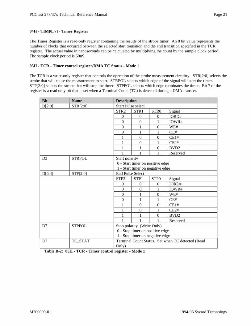
04H - TIM[0..7] - Timer Register
The Timer Register is a read-only register containing the results of the strobe timer. An 8 bit value represents thenumber of clocks that occurred between the selected start transition and the end transition specified in the TCRregister. The actual value in nanoseconds can be calculated by multiplying the count by the sample clock period.The sample clock period for the PCCtest 2xx/3xx is 50nS. A write to this register has no effect.
05H - TCR - Timer control register
The TCR is a write-only register that controls the operation of the strobe measurement circuitry. STR[2:0] selects thestrobe that will cause the measurement to start. STRPOL selects which edge of the signal will start the timer.STP[2:0] selects the strobe that will stop the timer. STPPOL selects which edge terminates the timer.
Bit Name DescriptionD[2:0] STR[2:0] Start Pulse select
STR2 STR1 STR0 Signal0 0 0 IORD#0 0 1 IOWR#0 1 0 WE#0 1 1 OE#1 0 0 CE1#1 0 1 CE2#1 1 0 Reserved1 1 1 Force VS1# low (PCCtest
270/370/273/373 only)D3 STRPOL Start polarity
0 - Start timer on positive edge 1 - Start timer on negative edge
D[6:4] STP[2:0] End Pulse SelectSTP2 STP1 STP0 Signal
0 0 0 IORD#0 0 1 IOWR#0 1 0 WE#0 1 1 OE#1 0 0 CE1#1 0 1 CE2#1 1 0 Reserved1 1 1 Force VS2# low (PCCtest
270/370/273/373 only)D7 STPPOL Stop polarity
0 - Stop timer on positive edge 1 - Stop timer on negative edge
Table A-2: Offset 05H TCR - Timer Control Register

Page 18 PCCtest 27x/37x Technical Reference Manual
1994-96 Sycard Technology M200009-01
06H - MISC - Control Register
The MISC Control register is a read/write register that contains various control bits for the PCCtest unit.
Bit Name DescriptionD[0:1] ALSEL[0:1] External Latch Select - Controls which of the three 8 bit
address latches is to be read from the LADD register atoffset 02hALSEL1 ALSEL0 Address Latch Selected0 0 Reserved0 1 Address Latch A[10:3]1 0 Address Latch A[18:11]1 1 Address Latch A[25:19]
D[2:3] WAIT[0:1] Wait State Select - control the number of wait states thatare inserted for any I/O or memory accessWAIT1 WAIT0 Wait States0 0 None0 1 See section 3.101 0 See section 3.101 1 See section 3.10
D4 TS1 Tri-State Control. Tri-states the following signalsBVD1BVD2READYWPCD1#CD2#WAIT#INPACK#
D5 INPACK_EN 0 = INPACK# not generated1 = INPACK# generated on all I/O reads
D6 ARM ARM bit for address latching. A zero to one transition ofthis bit arms the external address latches. The state of theaddress bus on read/write access immediately followingthis ARM will be latched.
D7 WAIT2 For revision 1.03 and higher PCCtest units only. Seesection 3.10
Table A-3: Offset 06H - MISC - Control Register
PCCtest 27x/37x Technical Reference Manual Page 19
M200009-01 1994-96 Sycard Technology
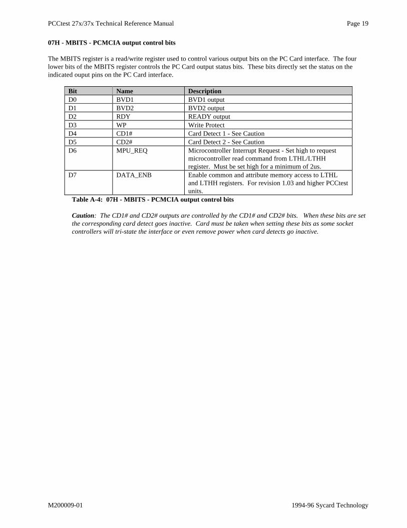
07H - MBITS - PCMCIA output control bits
The MBITS register is a read/write register used to control various output bits on the PC Card interface. The fourlower bits of the MBITS register controls the PC Card output status bits. These bits directly set the status on theindicated ouput pins on the PC Card interface.
Bit Name DescriptionD0 BVD1 BVD1 outputD1 BVD2 BVD2 outputD2 RDY READY outputD3 WP Write ProtectD4 CD1# Card Detect 1 - See CautionD5 CD2# Card Detect 2 - See CautionD6 MPU_REQ Microcontroller Interrupt Request - Set high to request
microcontroller read command from LTHL/LTHHregister. Must be set high for a minimum of 2us.
D7 DATA_ENB Enable common and attribute memory access to LTHLand LTHH registers. For revision 1.03 and higher PCCtestunits.
Table A-4: 07H - MBITS - PCMCIA output control bits
Caution: The CD1# and CD2# outputs are controlled by the CD1# and CD2# bits. When these bits are setthe corresponding card detect goes inactive. Card must be taken when setting these bits as some socketcontrollers will tri-state the interface or even remove power when card detects go inactive.

Page 20 PCCtest 27x/37x Technical Reference Manual
1994-96 Sycard Technology M200009-01
Appendix B Register Description Mode 1
This section describes the configuration of the PCCtest registers when the PCCtest is configured for MODE 1operation. MODE 1 is entered via a LOAD_MODE1 command described in section 4.6. MODE 1 registers are usedto command the PCCtest to execute Direct Memory access tests of the PC Card interface. All PCCtest registers arewritten via I/O write commands. There are 8 writable 8 bit registers within the PCCtest unit. All I/O write strobes(IOWR#) qualified by a chip enable (CE1#) will write to one of the PCCtest registers. A[2:0] will select whichregister is written by the I/O write strobe. Mode 1 is supported in the PCCtest 260/360/270/370/273/373 modelsonly.
00H - LTHL - Low Data Byte to PC card bus - Mode 1
Any memory write (WE#) qualified with a valid CE1# will cause the LTHL register to be updated with contents ofthe PC card data bus (D[7:0]). In addition an I/O write qualified with CE1# and A[0:2] = 000 will also cause a writeto this register.
Any memory read qualified with a valid CE1# will cause the value of the LTHL register to gated onto the PC carddata bus (D[7:0]). For revision 1.03 and higher PCCtest units, DATA_ENB in MBITS register must be high to readfrom LTHL. An I/O read qualified with CE1# and A[0:2] = 000 will gate the contents of LTHL onto the PC Carddata bus.
01H - LTHH - High Data Byte to PC card bus - Mode 1
Any memory write memory qualified with a valid CE2# will cause the LTHH register to be updated with contents ofthe PC card data bus (D[15:7]).
Note: An 8 bit I/O write to the LTHH register is not possible.A memory read qualified with a valid CE2# will cause the value of the LTHL register to gated onto the PC card databus (D[15:8]). For revision 1.03 and higher PCCtest units, DATA_ENB in MBITS register must be high to read fromLTHH. An 8 bit I/O read qualified by CE1# and A[0:2] = 001 will gate the contents of LTHH onto the PC Card databus D[7:0].
02H - TRST - Reset strobe to pulse counter - Mode 1
A write to the TRST register will arm the strobe timer circuitry. Once a write to the TRST register is complete, thecounter will be armed and waiting for the selected PC card strobe.
03H - LOW_LATCH - Control latch
LOW_LATCH is a read-only register containing the latched values of the various select and lower order addresslines. These signals are latched in the same method as the upper order address bits are latched, by using the ARM bitin the MISC Control Register.
Bit Name DescriptionD[2:0] Not UsedD3 LREG Latched PC card #REGD4 LCE1N Latched PC card #CE1D5 LCE2N Latched PC card #CE2D6 EIN0 Not usedD7 EIN1 PCMCIA RESET signal status
Table B-1 - 03H - LOW_LATCH - Control Signal Latch
PCCtest 27x/37x Technical Reference Manual Page 21
M200009-01 1994-96 Sycard Technology
04H - TIM[0..7] - Timer Register
The Timer Register is a read-only register containing the results of the strobe timer. An 8 bit value represents thenumber of clocks that occurred between the selected start transition and the end transition specified in the TCRregister. The actual value in nanoseconds can be calculated by multiplying the count by the sample clock period.The sample clock period is 50nS.
05H - TCR - Timer control register/DMA TC Status - Mode 1
The TCR is a write-only register that controls the operation of the strobe measurement circuitry. STR[2:0] selects thestrobe that will cause the measurement to start. STRPOL selects which edge of the signal will start the timer.STP[2:0] selects the strobe that will stop the timer. STPPOL selects which edge terminates the timer. Bit 7 of theregister is a read only bit that is set when a Terminal Count (TC) is detected during a DMA transfer.
Bit Name DescriptionD[2:0] STR[2:0] Start Pulse select
STR2 STR1 STR0 Signal0 0 0 IORD#0 0 1 IOWR#0 1 0 WE#0 1 1 OE#1 0 0 CE1#1 0 1 CE2#1 1 0 BVD21 1 1 Reserved
D3 STRPOL Start polarity 0 - Start timer on positive edge 1 - Start timer on negative edge
D[6:4] STP[2:0] End Pulse SelectSTP2 STP1 STP0 Signal
0 0 0 IORD#0 0 1 IOWR#0 1 0 WE#0 1 1 OE#1 0 0 CE1#1 0 1 CE2#1 1 0 BVD21 1 1 Reserved
D7 STPPOL Stop polarity (Write Only) 0 - Stop timer on positive edge 1 - Stop timer on negative edge
D7 TC_STAT Terminal Count Status. Set when TC detected (ReadOnly)
Table B-2: 05H - TCR - Timer control register - Mode 1

Page 22 PCCtest 27x/37x Technical Reference Manual
1994-96 Sycard Technology M200009-01
06H - MISC - Control Register - Mode 1
The MISC Control register is a read/write register that contains various control bits for the PCCtest unit.
Bit Name DescriptionD0 DMA_EN DMA Enable (Write only)D1 Not UsedD[2:3] WAIT[0:1] Wait State Select - The Wait state generator will generate
wait states during a DMA transfer, however in an ISAenvironment the wait states will be ignored.WAIT1 WAIT0 Wait States0 0 None0 1 See section 3.101 0 See section 3.101 1 See section 3.10
D4 TS1 Tri-State Control. Tri-states the following signalsBVD1BVD2READYWPCD1#CD2#WAIT#INPACK#
D5 INPACK_EN 0 = INPACK# not generated1 = INPACK# generated on all I/O reads
D6 Not UsedD7 WAIT2 For revision 1.03 and higher PCCtest units only. See
section 3.10Table B-3: 06H - MISC - Control Register - Mode 1

PCCtest 27x/37x Technical Reference Manual Page 23
M200009-01 1994-96 Sycard Technology
07H - MBITS - PCMCIA output control bits/DMA Complete Status - Mode 1
The MBITS register is a read/write register used to control various output bits on the PC Card interface. The fourlower bits of the MBITS register controls the PC Card output status bits. These bits directly set the status on theindicated ouput pins on the PC Card interface.
Bit Name DescriptionD0 BVD1 BVD1 outputD1 BVD2 BVD2 outputD2 RDY READY outputD3 WP Write ProtectD4 CD1# Card Detect 1D5 CD2# Card Detect 2D6 MPU_REQ Microcontroller Interrupt Request - Set high to request
microcontroller read command from LTHL/LTHHregister. Must be set high for a minimum of 2us.
D7 DMA_COMP Set if DMA transfer completeTable B-4: MBITS - PCMCIA output control bits/DMA Complete Status - Mode 1
Caution: The CD#1 and CD2# outputs are controlled by CD1# and CD2#. When these bits are set thecorresponding card detect goes inactive. Card must be taken when setting these bits as some socketcontrollers will tri-state the interface or even remove power when card detects go inactive.

Page 24 PCCtest 27x/37x Technical Reference Manual
1994-96 Sycard Technology M200009-01
Appendix C Microprocessor Commands
The following table of PCCtest microprocessor assisted command are available on the PCCtest model 270./370.Access to these command is described in section 4.0 of this document.
Command Description CMD ModeMEASURE_VCC Measure Vcc - Return value in LTHL 010H Mode 0MEASURE_VPP1 Measure Vpp1 - Return value in LTHL 011H Mode 0MEASURE_VPP2 Measure Vpp2 - Return value in LTHL 012H Mode 0MEASURE_SIGNAL Measure RESET signal level - Return value in LTHL 012H Mode 0REQUEST_MAJOR Request Major Revision Number - Returned in LTHL 041H Mode 0REQUEST_MINOR Request Minor Revision Number - Returned in LTHL 042H Mode 0REQUEST_MODEL Request Model Number - Returned in LTHL 043H Mode 0GET_ROM_SUM Get EPROM checksum - Returned in LTHL 050H Mode 0OUT_SPEAKER Output 1KHz tone to SPKR# output 060H Mode 0OUT_SPEAKER Output 1KHz tone to SPKR# output 060H Mode 0STROBE_CD1 Strobe CD1# for number of milliseconds specified in
LTHH register. Not supported on PCCtest230/330/273/373.
070H Mode 0
STROBE_CD2 Strobe CD2# for number of milliseconds specified inLTHH register. Not supported on PCCtest230/330/273/373.
071H Mode 0
LOAD_MODE0 Load TGA NORMAL configuration (MODE 0) 0C0H Mode 0LOAD_MODE1 Load TGA DMA configuration (MODE 1) 0C1H Mode 1DMA_COUNT0_CMD Load DMA count (LSB) 0B0H Mode 1DMA_COUNT1_CMD Load DMA count (MSB) 0B1H Mode 1DMA_WAIT_CMD Specify number of milliseconds to wait before starting
DMA transfer0B2H Mode 1
DMA_ROUTE_CMD -DREQ Routing - Specifies DMA routing and DMAwidth.Bit 0 - Set if DREQ = IOIS16Bit 1 - Set if DREQ = BVD2Bit 2 - Set if DREQ = INPACKBit 6 - Set if 16 bit DMABit 7 - Set if DMA Read (IOWR)
0B3H Mode 1
DMA_ABORT_CMD DMA Abort time - Number of ms to wait after DREQbefore aborting DMA Transfer.
0B4H Mode 1
DMA_PAT_CMD DMA Pattern is Random code from on-boardmicrocontroller code ROM.xx - Select which page contains DMA data
0B5H Mode 1
DMA_START_CMD Start DMA Transfer after number of ms specified inthe DMA_WAIT_CMD
0B6H Mode 1
DMA_STAT_CMD Return DMA completion status00 - No error01 - Timeout error - No DACK02 - Data error, for DMA read only03 - Missing Terminal Count (TC)05 - Premature TC
0B7H Mode 1
Table C-1a - Microprocessor Assisted Command List

PCCtest 27x/37x Technical Reference Manual Page 25
M200009-01 1994-96 Sycard Technology
Command Description CMD ModeDMA_PAT2_CMD Select DMA Pattern - Standard Patterns
00 - Invalid Value - Do not use01 - Incrementing data pattern02 - Decrementing data pattern03 - Walking 1 pattern04 - Walking 0 pattern05 - ASCII Pattern
0B8H Mode 1
DMA_ENTER_CMD Place PCCtest into DMA mode 0B9H Mode 1SEND_SERIAL Send data to serial port - Data contained in LTHH
This command supported in PCCtest 270/370/273/373only
0D0H Mode 0
GET_SERIAL Receive data from serial port - Data returned in LTHHThis command supported in PCCtest 270/370/273/373only
0D1H Mode 0
Table C-1b - Microprocessor Assisted Command List