


PCB-June2011.pdf
69
June 2011 • The PCB Magazine 1 Should You Be Using a High-Frequency Laminate Instead of FR-4? by John Coonrod Thin Laminates: Buried Capacitance or What? by Istvan Novak Materials for High- Reliability Applications by Yash Sutariya Does America Need Manufacturing? by Steven Williams 10 16 22 38 PCB MATERIALS June 2011
Transcript of PCB-June2011.pdf

June 2011 • The PCB Magazine 1
Should You Be Using a High-Frequency Laminate Instead of FR-4? by John Coonrod
Thin Laminates: Buried Capacitance or What?by Istvan Novak
Materials for High- Reliability Applications by Yash Sutariya
Does America Need Manufacturing? by Steven Williams
10
16
22
38
PC
B M
AT
ERIA
LSJune 2011
Electronics Materials
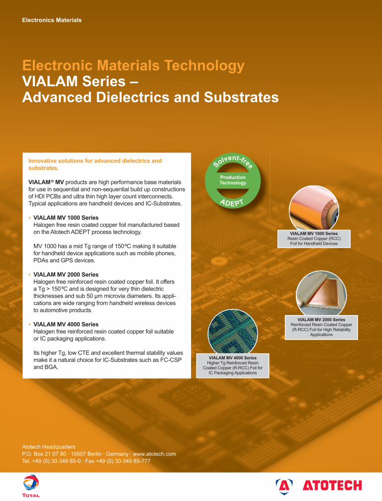
Electronic Materials TechnologyVIALAM Series – Advanced Dielectrics and Substrates
Atotech HeadquartersP.O. Box 21 07 80 · 10507 Berlin · Germany · www.atotech.comTel. +49 (0) 30-349 85-0 · Fax +49 (0) 30-349 85-777
Innovative solutions for advanced dielectrics and substrates.
VIALAM ® MV products are high performance base materials for use in sequential and non-sequential build up constructions of HDI PCBs and ultra thin high layer count interconnects. Typical applications are handheld devices and IC-Substrates. VIALAM MV 1000 Series
Halogen free resin coated copper foil manufactured based on the Atotech ADEPT process technology.
MV 1000 has a mid Tg range of 150 ºC making it suitable for handheld device applications such as mobile phones, PDAs and GPS devices.
VIALAM MV 2000 SeriesHalogen free reinforced resin coated copper foil. It offers a Tg > 150 ºC and is designed for very thin dielectric thicknesses and sub 50 μm microvia diameters. Its appli-cations are wide ranging from handheld wireless devices to automotive products.
VIALAM MV 4000 SeriesHalogen free reinforced resin coated copper foil suitable or IC packaging applications.
Its higher Tg, low CTE and excellent thermal stability values make it a natural choice for IC-Substrates such as FC-CSP and BGA.
VIALAM MV 1000 SeriesResin Coated Copper (RCC)
Foil for Handheld Devices
VIALAM MV 2000 SeriesReinforced Resin Coated Copper (R-RCC) Foil for High Reliability
Applications
VIALAM MV 4000 SeriesHigher Tg Reinforced Resin
Coated Copper (R-RCC) Foil for IC Packaging Applications
Solvent-free
ADEPT
ProductionTechnology

June 2011 • The PCB Magazine 3
If you’re reading this, you are just one click away from the all-digital, The PCB Magazine! This month, we present even more of the relevant and compelling content, including feature articles, videos, and interviews that has the PCB industry buzzing. That “buzz” has resulted in a steady stream of positive feedback from around the globe, and for that, we say THANK YOU!
If you haven’t already done so, don’t wait another minute to subscribe, and have The PCB Magazine delivered right to you inbox each month.
Features on PCB MaterialsThis month, it’s a material world—and our
contributors have plenty to say on the subject:In our first feature, Should You Be Using
a High-Frequency Laminate Instead of FR-4?, John Coonrod, of Rogers Corporation, reports on the reliability and affordability of epoxy-based FR-4 circuit board materials, and why they are not the answer for every circuit.
Next, Oracle’s Istvan Novak takes on the controversial topic of thin laminates in his feature, Thin Laminates: Buried Capacitance or What? In it, Novak examines the electrical properties of thin laminates, and addresses their needs, benefits and uses.
In Materials for High-Reliability Applications, Saturn Electronic Corporation’s Yash Sutariya points out that discussions of high reliability materials for printed circuit board applications usually include strong opinions: is one material system versus another better, or is it materials’ properties that imply reliability?
Rounding out our June Feature Articles is Insulectro’s Ken Parent, with No Time Like Now! The Peril and Thrill of Being a Tech Early Adopter. Parent stresses the importance of timing, with regard to technology advancement, and whether there is ever a perfect time to “jump in.”
This Month’s Video InterviewsOur June issue also contains Feature
Videos that don’t disappoint. Straight from IPC APEX EXPO, our “Real Time with…” series includes provocative discussions on hot topics: Global Laminates President Bruce Hurley in his overview of the technology and its benefits to the industry with New Ceramic Core Material Beats the Heat; Oak-Mitsui Technologies VP John Andresakis, discussing how his company differentiates itself in the market with Copper Foil Technology: A Fine Balance; and Greg Bull of Rogers Corporation discussing its new material in Rogers New High-Frequency Laminate.
June ColumnsColumnists this month include regulars
Paul Reid and Karl Dietz, and our newest addition, Point of View by industry veteran Steven Williams. Dale Smith is also back with the second of five installments on Lean Manufacturing.
We hope you enjoy the June issue of The PCB Magazine, and don’t hesitate to let us know what you think!
Here’s what’s happening in the June Issue of The PCB Magazine!
June 2011 • The PCB Magazine 3
int
ro
du
ct
ionThey have arrived — New advaNced PcB maTerials

4 The PCB Magazine • June 2011
Features—pcb materialsShould You Be Using a High-Frequency Laminate Instead of FR-4?by John coonrod
Thin Laminates: Buried Capacitance or What?by istvan novak
Materials for High-Reliability Applications: All IPC-4101-Grouped Materials are not Created Equalby Yash sutariya
No Time Like Now! The Peril and Thrill of Being a Tech Early Adopterby Ken parent
columnsOnshoring—Can We Bring PCBs Back from China?by ray rasmussen
Does America Need Manufacturing?by steven Williams
Repeat Defectsby Karl H. dietz
How to Implement Lean Manufacturing into a Printed Circuit Board Shop, Part 2 by dale smith
Microvia Separationby paul reid
Chinaby barry matties
neWsTop Ten Most-Read News Highlights from PCB007 This Month
articlesPCB Design Techniques for DDR, DDR2 & DDR3, (Part 2)by barry olney
What It Takes to Thrive: The Research and Experimentation (R&E) Tax Creditan interview with Hunter technology
Video sHortsCopper Foil Technology: A Fine Balance
New Ceramic Core Material Beats the Heat
Rogers’ New High-Frequency Laminate
Europe: Ready for Change
sHortsASC Earns Military Polyimide Qualification
Arlon Introduces New Composite Material
Maskless Lithography Welcomes Two Senior Executives
All Flex Minneapolis Facility Completes Upgrade, Expansion
Honeywell Relies on Standards to Set Contractor Expectations
Atotech to Enhance Technology; Collaborate with CWRU
extrasEvents Calendar
Advertisers Index & Masthead
co
nt
en
ts
NeW
AD
vAN
CeD
PC
B MATeRIA
LS
10
16
22
28
6
38
46
50
56
66
62
32
42
15
20
27
31
915
20
44
49
55
64
69
JUNe 2011
voLUMe 1
NUMBeR 2
THe DeFINITIve
INTeRACTIve MAgAzINe
DeDICATeD To THe
gLoBAL PCB INDUSTRY
www.pcb007.com

6 The PCB Magazine • June 2011
Onshoring —Can We Bring PCBs Back from China?
by Ray RasmussenI-CoNNeCt007
it is going take more than increased labor rates, harsher environmental penalties, and subsidies to motivate pcb multinationals to begin even thinking about bringing work back home.
s u m m a r Y
I’ve read quite a few articles about the return of manufacturing to the U.S., and what it would take to make that happen. In fact, we’ve published a few ourselves. It’s an intriguing idea and certainly plays well in the mainstream press and on Capitol Hill. As much as I like the idea, I can’t see how it would work for PCBs; it’s a lot more complicated than it seems on the surface. In fact, it’s way too little, too late.
Yes, China has had, and continues to have, unfair advantages such as manipulated currency exchange rates designed to favor their producers over the rest of the world, and subsidies, which have encouraged exports over the last decade. Both of these scenarios have spurred a huge shift of wealth from, mostly, the U.S. and Europe. However, as you can read in the mainstream and trade press, things are changing. Labor rates are increasing and the RMB (China’s currency) is under pressure from most of the developed world, resulting in a couple-point rise in the exchange rate over the last year or two. That’s not enough, but it’s a start. China has also come down hard on industries like PCBs, which use a lot of water and discharge a significant amount of heavy metals into their streams and rivers. This has slowed the unbridled expansion of the industry (at least in the East) and increased costs for compliance. It’s a slow process, but it does show that the tide is starting to turn. Still, it’s going take more than that before the PCB multinationals start to look at bringing work back home.
In a recent earnings report, Viasystems mentioned the rise of the cost of labor in China, which has increased 18-20% over the last year. In an interview, CEO David Sindelar gave this quote: “We don’t like inflation and our customers don’t like inflation, but it will take a long time before our costs in China get up to Western World levels.”
Companies like Viasystems are in China for the long haul
and won’t be moving PCB production back to the U.S. any time soon. They’ve made big investments in China and continue to do so (Viasystems just announced $100 million in capacity expansions).
Consumer Electronics InertiaNow, iPods, iPhones and iPads don’t
represent all the electronics China produces, but the consumer electronics industry has been the life’s blood of the Chinese PCB factories and represents the lion’s share of the business there. The Chinese have used lower-cost consumer electronics to develop their electronics-manufacturing base, following the examples left by the Japanese in the ‘70s and ‘80s, and the four tigers in the ‘80s and ‘90s. This massive effort by the Chinese has allowed the country to build an electronics infrastructure that is self-sustaining; they have almost all they need, including rare earth metals (China produces 95% of the world’s supply). Another thing they have going for them is their huge middle class, which will buy more and more consumer products in the years to come. (Chinese consumers already
THe WAY I See IT
co
lu
mn

www.christopherweb.com714.979.7500
www.christopherweb.com714.979.7500
ON
STA
TIC TECHNOLOGY C
OMP
AN
Y
Christopher Associates has your circuit boards covered
with the latest world-class technologies and finishes!
Christopher Associates has your circuit boards covered
with the latest world-class technologies and finishes!
CSUN’S SMO OVEN SERIESDesigned specifically for the photoimageable process, CSUN incorporates many features that guarantee excellent curing. The SMO-7A boasts a Temperature uniformity of ±1.5C!
CSUN’S SMO OVEN SERIESDesigned specifically for the photoimageable process, CSUN incorporates many features that guarantee excellent curing. The SMO-7A boasts a Temperature uniformity of ±1.5C!
OTC LPI SOLDER MASKSOTC, the leading supplier of solder masks in China, manufactures a complete line of LPI solder mask colors and finishes needed for North America’s quick-turn, prototype market. OTC's R-500 series meets all industry standards and is accepted world-wide by all major endusers.
OTC LPI SOLDER MASKSOTC, the leading supplier of solder masks in China, manufactures a complete line of LPI solder mask colors and finishes needed for North America’s quick-turn, prototype market. OTC's R-500 series meets all industry standards and is accepted world-wide by all major endusers.
SPF (Semblant Plasma Finish)Patented SPF (Semblant Plasma Finish) improves PCBcorrosion resistance, extends shelf life, and enhances soldering capabilities. SPF is a 40 nm fluoropolymer coating for all PCB exposed surfaces and vias – including micro-fine elements. This ultra-thin film protects even the most intricate areas against both atmospheric and liquid corrosion. Applied at room temperature with a plasma polymerization process, SPF is both economically sound and environmentally friendly!The process uses no hazardous chemicals or heavy metals, and generates no waste water!
SPF (Semblant Plasma Finish)Patented SPF (Semblant Plasma Finish) improves PCBcorrosion resistance, extends shelf life, and enhances soldering capabilities. SPF is a 40 nm fluoropolymer coating for all PCB exposed surfaces and vias – including micro-fine elements. This ultra-thin film protects even the most intricate areas against both atmospheric and liquid corrosion. Applied at room temperature with a plasma polymerization process, SPF is both economically sound and environmentally friendly!The process uses no hazardous chemicals or heavy metals, and generates no waste water!
8 The PCB Magazine • June 2011
buy more PCs than U.S. consumers.) As a result, product manufacturers, EMS and OEMs not only get the benefit of low-cost PCBs, but also lower-cost components, assemblies and box-builds. Additionally, the PCB fabs buy their materials from multinational suppliers at Chinese prices. This, along with the growth of their own consumer market, is why we won’t see the return of volume PCBs to the U.S. or Europe anytime soon.
As you can see, the PCB is only part of the story. Without the rest of the supply chain to support lower-cost consumer products, there’s little chance for the resurgence of consumer PCBs in the West.
The Big Get BiggerWith about a third of
the world’s PCBs being manufactured in China along with most of the electronic products (by volume), there’s a ton of inertia driving that market. The energy from consumers around the globe, and at home, continues to feed the electronics industry in China, which is evidenced by the continued expansion of their PCB industry. Recently, I was forwarded an email with comments from Dr. Hayao Nakahara, arguably the world’s leading expert on that market, talking about the incredible new PCB capacity being added with more mega-factories being built. Here are some of the names he mentions: Wus, Nan Ya PCB, Evertek, Unimicron and Ruwel, GBM Yuanmao and Sanmina. Then Naka goes on to say: “I could use three or four pages to write about all these new plants and expansions.” Many, if not all, of these expansions were approved before the Chinese government started cracking down on new PCB plants. It would seem that this next round of expansions is free to proceed. Future factories will likely have to be built further west or outside of China. We’ll see.
By the way, when I say “Chinese,” I mean the multinational companies doing business
in China. These are dedicated PCB fabricators in addition to those EMS providers that have their own Chinese PCB capabilities. I’m not talking about Chinese-owned PCB companies, which represent a small fraction of the market. I know we all tend to view the Chinese PCB industry as this single entity which has unfairly attacked our livelihoods, but it’s not the Chinese who are deciding to keep PCB production in China; it’s the Americans, the Europeans, the Japanese and Taiwanese, along with the Koreans. They’re the ones making the decisions to manufacture and expand in China. They’re in China to
serve their EMS or OEM customers who are also building their products in China. They (the OEM or EMS) get most of their components from other multinational suppliers doing business there, as well.
That Sucking SoundI think it’s safe to
say the Chinese gold rush of the last decade
is basically over. The flow of manufacturing to China has stopped and, in some cases, has actually returned. Most OEMs (tier 1 or 2 making lower-volume electronics), today, know that the perceived advantages of manufacturing in China really aren’t there when all things are considered. And, as costs continue to rise, China will stabilize with the rest of the world and keep the business that makes sense; the rest will go somewhere else. That will be the case for the U.S. as well. Business has stabilized and fabricators (those that are left) will find their niche. Those that do a good job will remain, and those who don’t will disappear. We’ll see growth in the U.S. for higher-tech PCBs used in military/aerospace, medical and industrial applications. Unless something changes, serious volume will still need to go somewhere else, perhaps to some mega-factory in China, India or Brazil.
“ We’ll see groWth in the U.s. for higher-tech PcBs
Used in military/aerosPace, medical and indUstrial
aPPlications. Unless something changes, serioUs volUme
Will still need to go someWhere else, PerhaPs to some mega-factory in china, india or Brazil. ”
ONSHORING—CAN WE BRING PCBS BACk FROM CHINA? continues

June 2011 • The PCB Magazine 9
Can We Compete? It does seem to me that these evermore
sophisticated fabricators in China (again, mostly multinationals) will make greater efforts to bring those capabilities into the Western markets and will have an advantage over their U.S.-only competitors. The expertise they’ve developed while building very hi-tech, high-volume boards for the likes of Apple in Asia will serve them well with those tier 2 OEMs and EMS providers back in the States. Being of a certain size has its advantages, and U.S.-only fabs will likely have to attain a certain size just to stay in the game.
There’s always the argument these Chinese fabricators can’t produce the quality and technology that those in the U.S. and Europe can. That may be true for the Chinese nationals, but not for the multinational companies. These are the guys who will continue to gain market share and, as a result, we will likely see more and more consolidation (Viasystems buying Merix, TTM buying Meadville, etc.).
What Will it Take to Compete?Go big, merge with other companies, find
backers, become global and compete head-to-head with the big guys. Heck, TTM was a nobody 10 years ago, and now they’re one of
the largest fabricators on the planet. If you elect to stay small and under the radar, then you’ve got to come up with a strategy that makes you unique. If you’re too small, how will you be able develop the technologies you need to stay competitive? That’s probably going to be the biggest challenge.
There may be opportunities for smaller companies to hang on to their market share by going beyond traditional PCBs. It may take a little chutzpah, but there are opportunities with some new interconnect technologies, like printed electronics or Occam. Getting really good at something like this might make a smaller PCB company an acquisition target or open up opportunities for investments to grow and expand. One thing’s for sure: the huge volumes of PCBs being built in Asia, or the rest of the world, are there to stay. They won’t be coming back anytime soon. PCB
ray rasmussen is the publisher and chief editor for i-connect007 publications. He has worked in the industry since 1978 and is the former publisher and chief editor of Circuitree Magazine. ray can be contacted at: [email protected]
sH
or
t
ONSHORING—CAN WE BRING PCBS BACk FROM CHINA? continues
ASC eARNS MILITARY PoLYIMIDe QUALIFICATIoNamerican standard circuits, inc. (asc) which
specializes in the manufacture of high reliability pcbs for the military, defense and aerospace industries has applied for and received polyimide qualification under mil-prF-55110, amendment 3 and mil-prF-31032.
ceo anaya Vardya commented, “asc has a tremendous amount of experience and technical expertise in the manufacture of rF circuitry, as well as other high-reliability products. our technical commitment to this market is apparent in our numerous patents for thermally conductive material and adhesives. although we have manufactured product using polyimide material for a long time, we thought it a logical step to add the polyimide certification to our military certification. asc is committed to military manufacturing. the qualification provides official verification of the quality
we continue to provide with regard to our customers’ polyimide products.”
explaining the significant role of polyimide material for the pcb industry, steve sekenina of isola Group said, “polyimide materials offer the ability to operate in environments with extreme operating temperatures including severe assembly processing, multiple thermal excursions and other high reliability applications. polyimide materials are utilized in a wide variety of mission critical applications including military, avionics, burn-in boards, missile systems, satellites, down hole, and other demanding applications.”
american standard has been a provider of rF circuitry, high-reliability and thermally sensitive pcbs for the military, aerospace and commercial industries for more than nine years.

10 The PCB Magazine • June 2011
Fe
at
ur
e —
ne
W a
dV
an
ce
d p
cb
ma
te
ria
ls
Should You Be Using a High-Frequency Laminate Instead of FR-4?
Epoxy-based FR-4 circuit board materials are popular for a wide range of electronics applications, and for good reason. These low- cost, glass-reinforced substrates are reliable, with well-understood mechanical and electrical characteristics. They are used in everything from audio circuits to microwave designs. However, they are not the answer for every circuit, especially for a wide range of high-frequency designs, and for several reasons.
When trying to decide between FR-4 or a high-frequency laminate, the lower cost
of FR-4 may be important, but it may not be the only consideration. For example, how critical is signal loss to your design? In most passive circuits, such as filters, loss increases as frequency increases. FR-4 has a higher dissipation factor (Df) than laminates engineered for high-frequency use, and circuits fabricated on FR-4 will suffer higher losses than similar circuits formed on a high-frequency circuit. Typical values are about 0.020 for FR-4 and about 0.004 for a high-frequency laminate, or a dissipation factor that is about one-fourth that of FR-4. This translates into a meaningful difference in insertion loss between the two circuit-board materials. Some designs can tolerate a certain amount of loss, but it will depend upon the loss budget for a given project.
Another factor to consider when trying to choose between FR-4 and a high-frequency laminate is how those losses occur. Are they evenly distributed across the frequency band of operation? FR-4 is characterized by a Df that increases steadily with frequency, so as frequency rises, insertion loss increases. High-frequency laminates typically exhibit a more stable Df characteristic with frequency, with considerably less loss at higher frequencies.
by John Coonrodmarket development engineeradVanced circuit materials diVision roGers corp.
they may be reliable and affordable, but there are several reasons why epoxy-based Fr-4 circuit board materials are not the answer for every circuit, especially for a wide range of high-frequency designs.
s u m m a r Y
they have arrived!

June 2011 • The PCB Magazine 11
Figure 1 shows a comparison of insertion loss for simple microstrip circuits made on different materials of the same thickness.
Stable impedance is important to many designs, and this is another area where FR-4 and high-frequency laminates can deliver much different results. Stable impedance depends on maintaining a stable dielectric constant (Dk) across the length and width of a substrate, including as temperature changes. While they are low in cost, FR-4 materials can suffer relatively wide variations in Dk across the length and width of a circuit board, and with temperature. This can make it impossible, for example, to achieve flat amplitude response with frequency in an amplifier. High-frequency laminates, on the other hand, provide a Dk that remains constant across the length
and width of a board. This means more predictable performance in large circuits and more repeatable performance in multiple similar circuits formed from the same board.
For designs that must perform over temperature, FR-4 and high-frequency laminates can also provide very different results. To evaluate performance variations with temperature, circuit-board materials are characterized by the thermal coefficient of dielectric constant (TCDk). It is simply a measure of how much the dielectric constant changes over a defined temperature range. For FR-4, it is typically 200 parts per million (ppm) per degree Celsius (°C) change in temperature. While that might seem like a small number, it can result in large variations over a wide temperature range. Compare
“ staBle imPedance is imPortant to many designs, and this is another area Where fr-4 and high-freqUency laminates can deliver mUch different resUlts. ”
Figure 1. insertion loss comparisons for microstrip circuits using different materials.

12 The PCB Magazine • June 2011
it to about 40 ppm/°C for high-frequency laminates, a much smaller number resulting in much less variations with temperature. If a circuit must work with little variation over a wide temperature range, a high-frequency laminate is probably a better choice than FR-4. Comparisons of different circuit materials are shown in Figure 2, regarding TCDk.
Sometimes, the very value of a circuit board’s Dk can play an important part in choosing a particular material. In a wavelength-dependent circuit, such as an RF or microwave design, the value of the dielectric constant will impact the size of the circuit’s transmission lines, and thus the size of the circuit. Simply put, circuit-board materials with higher Dk values can yield smaller circuits. If the size of a circuit is important, then the value of the Dk should be part of the decision process in choosing a circuit-board material. FR-4 typically has
a Dk of about 4.5. That’s higher than most PTFE high-frequency materials, but lower than a number of high-frequency laminates which offer Dk values of 6.15, and even as high as 11.0. Using materials with these higher values can shave 25% or more off the size of a circuit built on FR-4. A typical example of the miniaturization of a microstrip filter circuit element is shown in Figure 3.
There are several other factors to consider when deciding between FR-4 and a high-frequency laminate, including the type of operating environment and the power/thermal requirements. For circuits where moisture might be a problem, for example, most high-frequency laminates have much lower moisture absorption than FR-4, which can be critical in outdoor applications. Also, high-frequency thermoset-based laminates may be more thermally robust than FR-4, and better able to handle the high temperatures of lead-free soldering processes.
Figure 2. tcdk curves for several high-frequency laminates as well as Fr-4 (epoxy/WG).
SHOULD YOU BE USING A HIGH-FREQUENCY LAMINATE INSTEAD OF FR-4? continues
tH
eY H
aV
e ar
riV
ed —
neW
ad
Va
nc
ed p
cb
ma
ter
ials

14 The PCB Magazine • June 2011
What is the best way to decide if your project might work better with a high-frequency laminate than with FR-4? Size up the electrical and mechanical requirements for the job, and see how they might be handled, first by FR-4 and then using a high-frequency laminate. For ease of comparison, data sheets are readily available for both types of circuit board materials and provide the key facts on electrical and mechanical parameters and tolerances. If the mechanical and electrical variations of FR-4 are too wide for your application, consider paying a bit more for a high-frequency laminate, but with much improved performance and reliability. In the end, the higher yields from using a dielectric material with tighter manufacturing tolerances, such as RO4000® thermoset substrates, might even mean lower production costs than when using FR-4. PCB
RO3000, RO3035, RO4000, RO4350B and LoPro are licensed trademarks of Rogers Corporation.
Figure 3. example of possible circuit size reduction due to using a substrate with a higher dielectric constant.
John coonrod is a market development engineer for rogers corporation, advanced circuit materials division. He has more than 24 years experience in the pcb industry, about half of
which was in the Flexible printed circuit board industry doing circuit design, applications, processing and materials engineering. John has also supported the High Frequency rigid printed circuit board materials made by rogers for the past 10 years. reach John coonrod at [email protected].
SHOULD YOU BE USING A HIGH-FREQUENCY LAMINATE INSTEAD OF FR-4? continues
tH
eY H
aV
e ar
riV
ed —
neW
ad
Va
nc
ed p
cb
ma
ter
ials

June 2011 • The PCB Magazine 15
Vid
eo
int
er
Vie
W
John andresakis, Vice president of strategic technologies with oak-mitsui technologies, discusses copper foil, how his company differentiates itself in the market, and the efforts to reduce the copper foil profile while maintaining adhesion. oak-mitsui has been selling embedded materials for years, and John talks about the growing interest in these materials.
Copper Foil Technology: A Fine Balanceby Real Time with...Designers Forum
www.realtimewith.com
sH
or
t
ARLoN INTRoDUCeS NeW CoMPoSITe MATeRIALarlon materials for electronics announces
the introduction of Genclad 280 bond-ply, a proprietary woven fiberglass reinforced, ceramic-filled composite material engineered for optimal cost/performance efficiency in multi-layer rF and high frequency pcbs. combining a non-polar thermoset resin system with controlled-expansion ceramic filler and a low-loss thermoplastic material, Genclad offers next generation electrical performance that matches the electrical performance of traditional ptFe laminate systems, but offers designers the ability to use cost-effective multi-layer designs.
Genclad 280 is engineered for use in bonding dissimilar and hard-to-bond materials in multilayer pcb structures, particularly in high speed and microwave applications. compatible with ptFe laminate materials, Genclad 280 pre-preg processes in conventional Fr-4 lamination cycles, yet offers
a unique combination of properties for high speed, high frequency, multi-layer applications:
• Low dielectric constant and loss (2.8/0.002 at 10 GHz);• Low water absorption (0.04%);• Stable dielectric constant over frequency and temperature;• Excellent adhesion to a variety of PTFE and other rF/microwave cores;• High Decomposition Temperature (443°c) and t288 (>>60 sec) for lead-free solder compatibility;• Low Z-direction CTE (45-50 ppm/°C) for enhanced ptH reliability; and• RoHS-Compliant.
contact arlon material for electronics at 909-863-1097 or visit www.arlon-med.com for additional information on Genclad 280 and other high-performance arlon materials.

16 The PCB Magazine • June 2011
Fe
at
ur
e —
ne
W a
dV
an
ce
d p
cb
ma
te
ria
ls
after the heated debate about the proper selection of bypass capacitors, probably the next-most controversial topic is thin laminates. are they really beneficial? do we really need them? can thin laminates help us eliminate many of the high-frequency bypass capacitors we’re accustomed to using? let’s look at the electrical properties of thin laminates.
s u m m a r Y
Thin LaminaTes: Buried Capacitance
or What?
by Istvan Novakoracle
After the heated debate about the proper selection of bypass capacitors, probably the next most controversial topic is thin laminates. Are they really beneficial? Do we really need them?
Since the early 1990s, thin laminates have been mostly marketed as buried capacitance, many times also suggesting, or at least implying, that by using thin laminates we can eliminate many of the high-frequency bypass capacitors on the board. Is it really possible? The answer lies in the electrical properties of thin laminates.
A pair of rectangular parallel sheet conductors, a power/ground layer pair, separated by dielectrics, as shown in Figure 1, creates static capacitance.
Figure 1: a pair of metal layers forms a parallel-plate capacitor.
The capacitance (C) is proportional to the dielectric constant of the laminate (eoer) and area of conductors (l*w) and inversely proportional to the dielectric thickness (h):
The dielectric constant of free space, e0 is 8.85 pF/m, and the er relative dielectric constant is around 4 for many of our PCB laminates. If we plug in l, w and h in meters, we get the capacitance in farads.
The expression tells us where the name “buried capacitance” comes from: A power-
they have arrived!
June 2011 • The PCB Magazine 17
“ so if We Use thin laminates for PoWer-groUnd layers, can We reallyeliminate many ByPass caPacitors from the Board? the ansWer is yes... ”
Thin LaminaTes: Buried Capacitance
or What? ground layer pair gives us capacitance buried in the stackup; we get more capacitance as we use thinner laminates and/or higher dielectric constants. A one-inch square power-ground pair of the popular 50 um (2-mil) buried capacitance laminate produces approximately 450 pF of capacitance. If we double the dielectric thickness, the capacitance goes down by a factor of two; if we cut the dielectric thickness in half, the capacitance doubles.
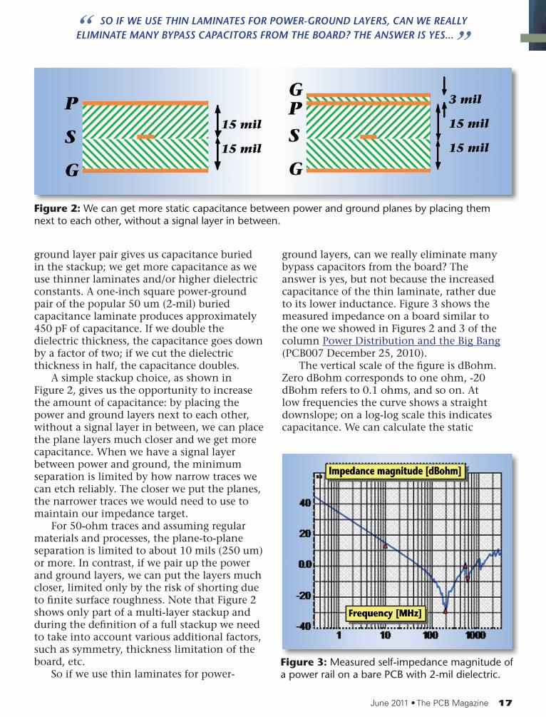
A simple stackup choice, as shown in Figure 2, gives us the opportunity to increase the amount of capacitance: by placing the power and ground layers next to each other, without a signal layer in between, we can place the plane layers much closer and we get more capacitance. When we have a signal layer between power and ground, the minimum separation is limited by how narrow traces we can etch reliably. The closer we put the planes, the narrower traces we would need to use to maintain our impedance target.
For 50-ohm traces and assuming regular materials and processes, the plane-to-plane separation is limited to about 10 mils (250 um) or more. In contrast, if we pair up the power and ground layers, we can put the layers much closer, limited only by the risk of shorting due to finite surface roughness. Note that Figure 2 shows only part of a multi-layer stackup and during the definition of a full stackup we need to take into account various additional factors, such as symmetry, thickness limitation of the board, etc.
So if we use thin laminates for power-
ground layers, can we really eliminate many bypass capacitors from the board? The answer is yes, but not because the increased capacitance of the thin laminate, rather due to its lower inductance. Figure 3 shows the measured impedance on a board similar to the one we showed in Figures 2 and 3 of the column Power Distribution and the Big Bang (PCB007 December 25, 2010).
The vertical scale of the figure is dBohm. Zero dBohm corresponds to one ohm, -20 dBohm refers to 0.1 ohms, and so on. At low frequencies the curve shows a straight downslope; on a log-log scale this indicates capacitance. We can calculate the static
Figure 2: We can get more static capacitance between power and ground planes by placing them next to each other, without a signal layer in between.
Figure 3: measured self-impedance magnitude of a power rail on a bare pcb with 2-mil dielectric.

18 The PCB Magazine • June 2011
PCB007.Com
capacitance for instance from the 60MHz frequency point, where the impedance magnitude is zero dBohm, or one ohm. This value corresponds to about 3nF static capacitance. At 200MHz the curve has a minimum, followed by an upslope, which corresponds to inductance. If for now we neglect the small resonances (we will cover those in later columns), we can approximate the curve with an average line, which goes through the zero dBohm value at 1GHz. This corresponds to about 150 pH inductance.
The 3nF static capacitance is not much on a power rail: unless the circuit draws very little power, we usually need orders of magnitude more capacitance to keep the impedance below our target value at lower frequencies. The real electrical benefit of the thin laminate comes from its low inductance. The inductance of a plane pair is approximately L[pH] = 33*h[mil], which yields 66 pH for our 2-mil plane separation in the above example. As opposed to the static capacitance of the laminate, which stays the same everywhere on the plane, inductance changes with location. It is the lowest in the middle of the plane and goes up rather sharply towards the sides and edges.
The impedance of Figure 3 was measured at one of the corners, this explains the 150 pH inductance value (instead of the 66 pH value expected from the 2-mil thickness). This inductance, however, even at the corner, is much lower than what we can achieve with a single bypass capacitor. In contrast, the inductance of a single bypass capacitor is usually around 1nH, at least ten times higher than the average inductance of a 2-mil plane pair.
Whether it is a discrete bypass capacitor or a power-ground plane pair, the impedance becomes inductive above the series
resonance frequency. At high frequencies, all that matters is the inductance, and thin laminates create very low inductance indeed. So, when it comes to thin laminates, think about their inductance rather their capacitance. PCB
Suggested Further Reading:1. John R. Sisler, “Method of making
multilayer printed circuit board,” US Patent 5,010,641, April 30, 1991.
2. James R. Howard and Gregory L. Lucas, “Capacitor laminate for use in capacitive printed circuit boards and methods of manufacture,” US Patent 5,079,069, January 7, 1992.
3. Joel S. Peiffer, “The history of embedded distributed capacitance,” Printed Circuit Design and Manufacture, August, 2004, pp. 32-37.
4. TecForum HP-TF2: “Thin PCB Laminates for Power Distribution. How Thin is Thin Enough?” February, 2002, DesignCon 2002. Available at www.electrical-integrity.com.
dr. istvan novak is a distinguished engineer at oracle, working on signal and power integrity designs of mid-range servers and new technology developments. novak received his m.s. degree from the
technical university of budapest, Hungary, and his ph.d. degree from the Hungarian academy of sciences in 1976 and 1989, respectively. With 25 patents to his name, novak is co-author of “Frequency-domain characterization of power distribution networks.” to contact istvan, click here.
For more information on this subject visit us online at: pcb007.com
THIN LAMINATES: BURIED CAPACITANCE OR WHAT? continues
tH
eY H
aV
e ar
riV
ed —
neW
ad
Va
nc
ed p
cb
ma
ter
ials


20 The PCB Magazine • June 2011
Vid
eo
int
er
Vie
W
Global laminates has introduced a new material, which is causing a stir in the industry as oems and their fab suppliers look for better thermal management solutions. Global laminates president bruce Hurley gives an overview of the technology and its benefits to the industry.
New Ceramic Core Material Beats the Heatby Real Time with...Electronics IPC Midwest
www.realtimewith.com
sH
or
t
MASkLeSS LITHogRAPHY WeLCoMeS TWo SeNIoR exeCUTIveS maskless lithography, a leading supplier of
direct-write, digital imaging (di) systems to the global pcb industry announced the appointment of two senior executives to its management team. Former Foxconn executive richard chenoweth was named Vice president of Global sales and marketing, and former sanmina-sci executive William pappani was named chief Financial officer.
the two new senior pcb industry executives will support the growing adoption of the company’s innovative di products. With an industry best cost-of-ownership and superior gray level imaging (Gli) technology, maskless’ award-winning, digital imaging technology is fast becoming the digital lithography of choice for the pcb industry as it moves away from contact printing, at 50-micron feature sizes.
“We are very pleased to welcome both bill and rich to our management team,” said dr. William elder, president and chief executive officer of maskless lithography. “the response by our customers to the new di systems has
been exceptionally positive. With demand accelerating, adding two seasoned pcb industry executives clearly strengthens our team as we deploy our new systems and support our expanding customer base throughout asia and north america.”
chenoweth has a wealth of pcb industry knowledge both in north america and throughout asia, particularly china. He has held senior management positions at Foxconn, Gbm, Flextronics and sanmina-sci. He has built successful global sales organizations, driving strategy and exceeding top-line growth goals.
pappani joined maskless from sanmina-sci where he served as Vice president of Finance and controller for the company’s pcb division. pappani drove efforts to expand the global footprint of sanmina, implemented a successful global integration strategy, and led gross-margin improvements at sanmina. He has traveled extensively throughout china, malaysia and singapore.


22 The PCB Magazine • June 2011
Fe
at
ur
e —
ne
W a
dV
an
ce
d p
cb
ma
te
ria
ls
When discussing high-reliability materials for printed circuit board applications, the conversation typically gears towards opinions of reliability: is one material system versus another better? other times, it’s materials’ properties that are stressed to imply reliability.
s u m m a r Y
Materials for High-Reliability Applications:All IPC-4101-Grouped Materials are not Created Equal
By Yash Sutariyasaturn electronics corporation/ saturn Flex sYstems, inc.
Materials Callouts One commonly cited document is the
IPC-4101C Specification for Base Materials for Rigid and Multilayer Printed Boards. This standard creates slash sheets, or “silos,” to combine like materials based on meeting product or performance characteristics such as resin type or a minimum Glass Transition (Tg) rating. In recent years, new slash sheets have been created to address materials capable for lead-free assembly that incorporates Glass Decomposition Temperature (Td).
For purposes of this discussion, we will focus on these lead-free capable materials.
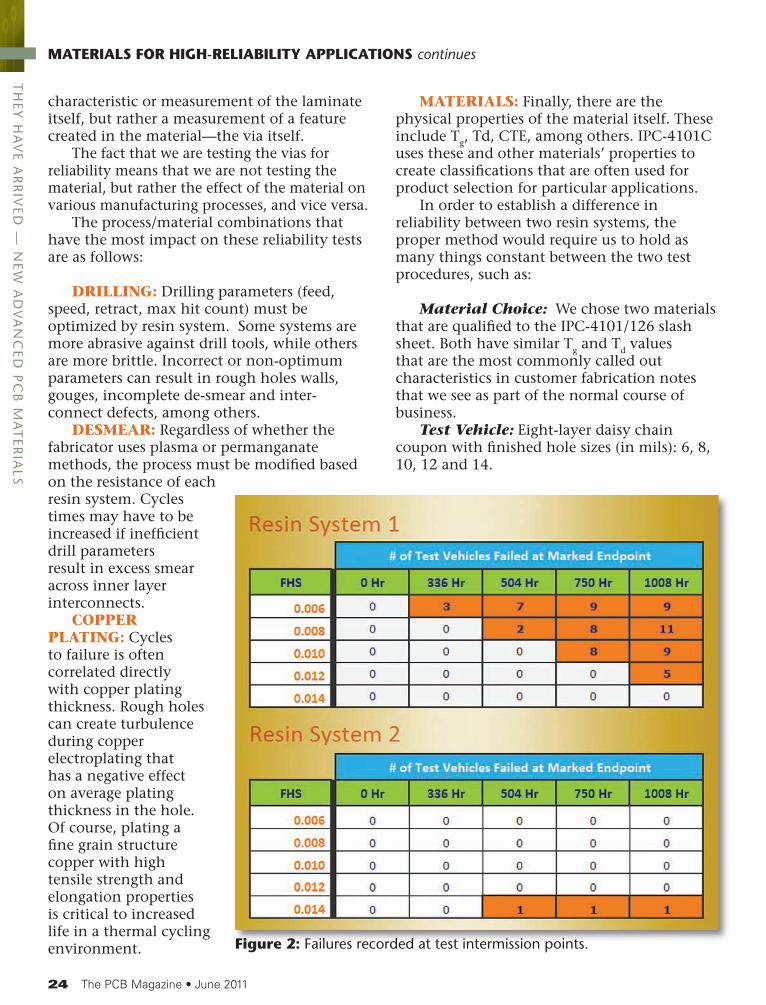
A summary table of three commonly called out standards is provided in Figure 1 for reference.
Once stacked next to each other, it’s easy to see why one could infer reliability via higher-level IPC categories and/or underlying materials properties such as Tg or Td. We argue, however, that these characteristics are almost meaningless when taken in a vacuum. They are merely indicators of the raw material, not the finished product, when it comes to reliability. Materials contribute only one part of a combination of systems that dictate the reliability of a product. In order to test the system, we have to undergo reliability testing.
Test MethodsThanks to our industrious friends on
the other side of the Great Wall, we’ve been pushed to diversify our customer base over the past decade away from our historical automotive supply base. This allowed us to experience a broad array of what people like to rely on for reliability testing. Industries we serve as a significant part of our business include Automotive, Military/Aerospace, Industrial Controls and Telecommunications.
Typically, the most intensive tests focus on via hole wall reliability. We’ll review a few of the common ones below.
they have arrived!
June 2011 • The PCB Magazine 23
Materials for High-Reliability Applications:All IPC-4101-Grouped Materials are not Created Equal
“ materials contriBUte only one Part of a comBination of systems that dictate the reliaBility of a ProdUct. ”
Delphi C7000 Delphi’s testing attempts to simulate real
operating conditions of the PCB by applying temperature cycling to Daisy Chain coupons. Each coupon contains a series of vias linked to each other through plated vias and inner layer connections. The test qualifies the vendor based on layer count and min via diameter. Testing is performed using two air-to-air test chambers. Standard parameters are five minutes transition time between peak temperatures, and 25 to 30 minutes at peak temperatures. Measurements are performed five times during the process, which terminates at 1000 cycles. Needless to say, this is not a quick test.
Highly Accelerated Thermal Shock (“HATS”)
The HATS test simulates the C7000 testing requirements by using an air-to-air thermal cycling procedure that rapidly heats and cools the test vehicles to the min and max temperatures by using a single chamber and introducing heated and cooled air. The benefit of this method is that it requires
approximately 1/6 to 1/7 the time required for the C7000 testing. However, there are schools of thought that believe this method is not as aggressive as the full thermal cycling required by Delphi’s testing.
Interconnect Stress Test (“IST”)IST is another accelerated method of
testing. Rather than use an air-to-air method to bring the test vehicles to temperature, this test method relies on an electrical charge to heat the coupon and stress the vias. To date, we are not aware of a direct correlation between this method and the previous air-to-air methods.
The main difference between these tests is how they attempt to stress the test vehicles. The main commonality is that they measure reliability based on resistance measurements of the daisy-chained vias.
Materials Comparison TestingBefore we discuss the reliability of one
material over another, it’s critical to establish why a particular material may display better reliability testing results. Notice that the reliability test results are not of a particular
Figure 1: ipc-4101 summary table.
24 The PCB Magazine • June 2011
MATERIALS FOR HIGH-RELIABILITY APPLICATIONS continues
characteristic or measurement of the laminate itself, but rather a measurement of a feature created in the material—the via itself.
The fact that we are testing the vias for reliability means that we are not testing the material, but rather the effect of the material on various manufacturing processes, and vice versa.
The process/material combinations that have the most impact on these reliability tests are as follows:
DRilling: Drilling parameters (feed, speed, retract, max hit count) must be optimized by resin system. Some systems are more abrasive against drill tools, while others are more brittle. Incorrect or non-optimum parameters can result in rough holes walls, gouges, incomplete de-smear and inter-connect defects, among others.
DeSmeaR: Regardless of whether the fabricator uses plasma or permanganate methods, the process must be modified based on the resistance of each resin system. Cycles times may have to be increased if inefficient drill parameters result in excess smear across inner layer interconnects.
CoPPeR PlaTing: Cycles to failure is often correlated directly with copper plating thickness. Rough holes can create turbulence during copper electroplating that has a negative effect on average plating thickness in the hole. Of course, plating a fine grain structure copper with high tensile strength and elongation properties is critical to increased life in a thermal cycling environment.
maTeRialS: Finally, there are the physical properties of the material itself. These include Tg, Td, CTE, among others. IPC-4101C uses these and other materials’ properties to create classifications that are often used for product selection for particular applications.
In order to establish a difference in reliability between two resin systems, the proper method would require us to hold as many things constant between the two test procedures, such as:
Material Choice: We chose two materials that are qualified to the IPC-4101/126 slash sheet. Both have similar Tg and Td values that are the most commonly called out characteristics in customer fabrication notes that we see as part of the normal course of business.
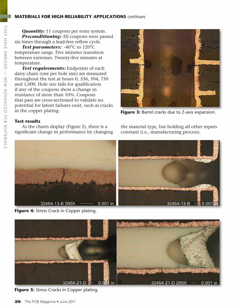
Test Vehicle: Eight-layer daisy chain coupon with finished hole sizes (in mils): 6, 8, 10, 12 and 14.
Figure 2: Failures recorded at test intermission points.
tH
eY H
aV
e ar
riV
ed —
neW
ad
Va
nc
ed p
cb
ma
ter
ials

Global leaders in testing.Industry pioneers in printing.
MicroCraft's history of Service and Supportfor Probe and Grid Testing, Fixturing andJetprint is unmatched in the industry.
www.usamicrocraft.com
Double/Quad Density Grids
Don't forget we also offer Testing and FixturingServices, offshore data prep and specializedInkjet printing services.
We have multiple 24-hour locations to serve you.To learn more or get a quote, please contact ustoday at [email protected].
26 The PCB Magazine • June 2011
MATERIALS FOR HIGH-RELIABILITY APPLICATIONS continues
Quantity: 11 coupons per resin system.Preconditioning: All coupons were passed
six times through a lead-free reflow cycle.Test parameters: -40°C to 120°C
temperature range. Five minutes transition between extremes. Twenty-five minutes at temperature.
Test requirements: Endpoints of each daisy chain (one per hole size) are measured throughout the test at hours 0, 336, 504, 750 and 1,000. Hole size fails for qualification if any of the coupons show a change in resistance of more than 10%. Coupons that pass are cross-sectioned to validate no potential for latent failures exist, such as cracks in the copper plating.
Test resultsAs the charts display (Figure 2), there is a
significant change in performance by changing the material type, but holding all other inputs constant (i.e., manufacturing process).
Figure 3: Barrel cracks due to Z-axis expansion.
Figure 4: stress crack in copper plating.
Figure 5: stress cracks in copper plating.
tH
eY H
aV
e ar
riV
ed —
neW
ad
Va
nc
ed p
cb
ma
ter
ials
June 2011 • The PCB Magazine 27
Yash sutariya is Vice president of corporate strategy at saturn electronics corporation (sec) and owner/president of saturn Flex systems, inc. (sFs). since joining the team, sec has successfully navigated
from a low-mix, high volume, automotive supplier to a high-mix, medium-to-high-volume diversified supplier to a broad range of industries. sutariya received his bba from the university of michigan, school of business administration.
MATERIALS FOR HIGH-RELIABILITY APPLICATIONS continues
Failure analysisFailures in this test can include blistering
and delamination, but are predominantly hole wall cracks or interconnect separations (Figures 3, 4 and 5).
The thermal cycling causes the material to expand and contract in the Z-axis. As seen in the photos at left, this can cause hole wall failures if the expansion is too great compared to the ability of the copper plating in the hole wall to adjust accordingly.
ConclusionWhen it comes to materials reliability, our
first stop is typically and IPC-4101 category, or a specific material property, such as CTE, Tg or Td. We have found that materials categorized into the same IPC slash sheet are not all equal.
Unfortunately, laminators trying to meet a particular value of a higher performance property can overlook other properties that sometimes are not found on a datasheet or
IPC- 4101 listing. The benefits of those properties can be easily diminished if the material diminishes the performance of other processes such as drilling or plating.
If true reliability is of utmost concern, the PCB user must qualify not only the resin system, but also the entire system used to produce the PCB to ensure that the fabricator and laminate system are compatible. PCB
Vid
eo
int
er
Vie
W
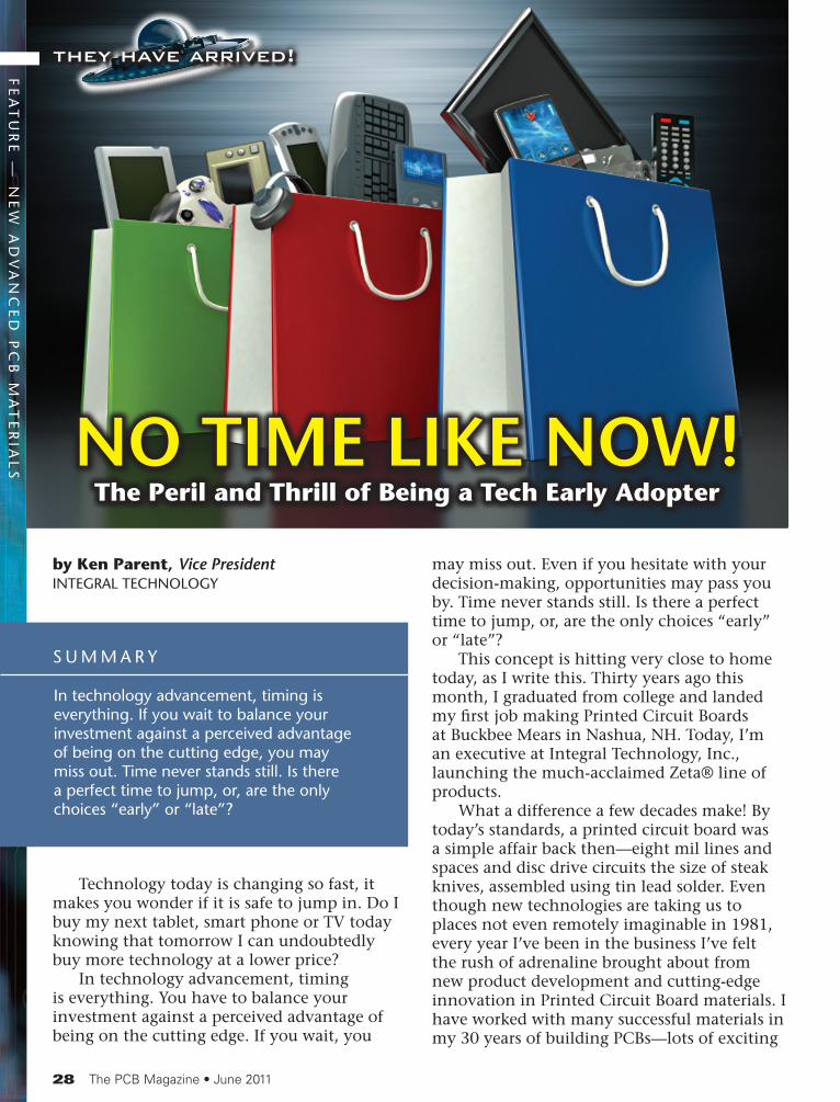
Greg bull of rogers corporation discusses rt/duroid 6035Htc High Frequency laminate, their new material that’s getting plenty of attention from designers, for its ability to manage heat. bull also explains more about his company and their new factory in china.
Rogers’ New High-Frequency Laminateby Real Time with...IPC APEX EXPO 2011
www.realtimewith.com
28 The PCB Magazine • June 2011
Fe
at
ur
e —
ne
W a
dV
an
ce
d p
cb
ma
te
ria
ls
in technology advancement, timing is everything. if you wait to balance your investment against a perceived advantage of being on the cutting edge, you may miss out. time never stands still. is there a perfect time to jump, or, are the only choices “early” or “late”?
s u m m a r Y
No TIMe LIke NoW! The Peril and Thrill of Being a Tech Early Adopter
by ken Parent, vice PresidentinteGral tecHnoloGY
may miss out. Even if you hesitate with your decision-making, opportunities may pass you by. Time never stands still. Is there a perfect time to jump, or, are the only choices “early” or “late”?
This concept is hitting very close to home today, as I write this. Thirty years ago this month, I graduated from college and landed my first job making Printed Circuit Boards at Buckbee Mears in Nashua, NH. Today, I’m an executive at Integral Technology, Inc., launching the much-acclaimed Zeta® line of products.
What a difference a few decades make! By today’s standards, a printed circuit board was a simple affair back then—eight mil lines and spaces and disc drive circuits the size of steak knives, assembled using tin lead solder. Even though new technologies are taking us to places not even remotely imaginable in 1981, every year I’ve been in the business I’ve felt the rush of adrenaline brought about from new product development and cutting-edge innovation in Printed Circuit Board materials. I have worked with many successful materials in my 30 years of building PCBs—lots of exciting
Technology today is changing so fast, it makes you wonder if it is safe to jump in. Do I buy my next tablet, smart phone or TV today knowing that tomorrow I can undoubtedly buy more technology at a lower price?
In technology advancement, timing is everything. You have to balance your investment against a perceived advantage of being on the cutting edge. If you wait, you
they have arrived!

30 The PCB Magazine • June 2011
times pioneering the public’s evolving thirst for electronics. Yet, nothing compares to the excitement of the new technologies available now. Today I am working with manufacturers and users of PCB materials that are innovating new technology and processes, which will reach far into our next generation of techno gadgets.
Integral Technology, Inc., was established to support the development, marketing and sales of new product technologies, advancing the use of existing products through new application techniques and market awareness as well as the technical engineering support and laboratory services. All of this leads to accomplishing objectives and servicing the industries we support.
Integral is headquartered in Orange County, California, where it has a research and development laboratory and engineering resources. Integral utilizes resources from around the world, working with companies that are leaders in their industry in developing groundbreaking technologies and next generation materials to meet tomorrow’s most critical challenges.
There are opportunities at all stages of the “innovation time line” that impact the cost (time and money) of bringing new ideas to the user. It’s an exciting process! Ideas lead to many things: critical thinking, developing, refining, crafting, testing and presenting, which in turn are enhanced by listening, scrapping (ouch), investing and consulting. Factor in the benefits of manufacturing, promoting, selling and servicing, add some rethinking, and revising, and you’ve got a net result that is a highly functional, effective portfolio of products—solutions TODAY for TOMORROW’s technology.
This process begins with an idea and evolves by developing solutions and processes that can be manufactured at an acceptable cost to the consumer. Innovative ideas create
products that drive revenue and profit. Simple, right? Not quite! I cannot do justice to this topic without paying some attention to IPC and UL, who want to make sure the products are safe and documented to specifications. Anyone who has worked in PCB electronics knows that UL and IPC’s involvement in the process is easy and creates no delays Okay, enough wishful thinking and back to the real world.
Our challenge as manufacturers is to create a streamlined process for bringing new materials to the end user. The reality of innovation is that it is hard work, expensive and takes a lot of time.
Everywhere, I hear a common desire to improve the time warp of product innovation, development and adoption—from the suppliers I work with in developing the materials, to the PCB manufacturers building with the materials and the OEMs designing the systems. We all want it better, faster and cheaper!
Integral Technology has developed a series of products around its Zeta® technology to help solve some of the industry’s most perplexing problems. For the last three years, we’ve been working on what we believe are breakthrough materials. The portfolio of Zeta products was spawned as a direct result of conversations with OEMs and suppliers about how to expand product lines and solve problems. The original idea was to solve a problem in lead-free assembly called pad cratering, which has been a silent, yet growing threat to the electronics business. Together, with all stakeholders, we were able to develop a solution to this emerging industry problem.
As we continue our trek to innovate, we will always listen to our customers and users of our products. This reconnaissance and vital feedback maps our progress towards new and expanded product offerings. As a result, we’ve been able to evolve our product portfolio to
NO TIME LIkE NOW! continues
“ this Process Begins
With an idea and
evolves By develoPing
solUtions and Processes
that can Be manUfactUred
at an accePtaBle cost
to the consUmer. ”
tH
eY H
aV
e ar
riV
ed —
neW
ad
Va
nc
ed p
cb
ma
ter
ials

June 2011 • The PCB Magazine 31
provide our customers new opportunities in High Density Interconnects. These new interconnect materials are fiberglass-free laminate and bonding materials that meet the needs of the next generation of electrical, mechanical and thermal demands due to the fact they are thin, high Tg, Low Dk and Low Df materials.
Integral Technology has made significant progress in testing the Zeta materials with PCB Manufacturers, Contract Manufacturers and OEMs in North America, Europe and Asia. Testing and evaluations have been focused on the need to improve lead free assembly yields, and drive higher layer count in thinner packages. This has been fueled by the curiosity to discover innovative ways to use the Zeta materials outside of our original product design scope.
It is exciting to imagine that our new Zeta family of products—revolutionary today—may be the new de facto standard of the future. Early adopters enjoy sustained benefits from
having had the courage and the intellect to recognize a game-changing product and jump in quickly. When the rest of the world catches up to you, you’ll be on to the next frontier. PCB
Ken parent is Vice president of product management for insulectro and Vice president of Vistana and integral technologies, inc. He started in the pcb business after graduating from Keene state
college with a bachelor of science degree in industrial engineering. parent held a process engineering position at buckbee mears company and lockheed martin (sanders associates) before moving from engineering to sales with a position at dynachem (morton international). He has been with insulectro in september of 2000.
Vid
eo
int
er
Vie
W
the european pcb industry continues to struggle as oems increasingly move work to asia. bernard bismuth discusses issues facing the industry, and some possible solutions that may just help the industry survive.
Europe: Ready for Changeby Real Time with...IPC APEX EXPO 2011
www.realtimewith.com

32 The PCB Magazine • June 2011
ar
tic
le
this second and last part in a series examining pcb design techniques will look at the comparison of ddr2 to ddr3; ddr3 design guidelines; pre-layout analysis; critical placement; an example of design rules; and finally, the post-layout analysis.
s u m m a r Y
PCB Design Techniques for DDR, DDR2 & DDR3
(Part 2)
by Barry Olney In-Circuit Design Pty Ltd, Australia
One major difference between DDR2 and DDR3 SDRAM is the use of levelling. To improve signal integrity and support higher frequency operations, the JEDEC committee defined a fly-by termination scheme used with the clocks, command and address bus signals. Fly-by topology reduces simultaneous switching noise (SSN) by deliberately causing flight-time skew between the data and strobes at every chip/DRAM, requiring controllers to compensate for this skew by adjusting the timing per byte lane (Table 1).
During a write, DQS groups are launched at separate times to coincide with a clock
DDR2/DDR3 Comparison DDR2 DDR3max clock Frequency 533/1066 800/1600odt static dynamicVdd 1.8V 1.5V (may also be 1.35V)Vtt 0.9V 0.75VVref 0.9V 0.75Vinput thresholds 0.9V 0.75Vmatch addr/cmd/ctrl to clK tightly yes yesmatch dQ/dmo/dsQ tightly yes yesmatch dQs to clock loosely yes not required
Table 1.

June 2011 • The PCB Magazine 33
PCB Design Techniques for DDR, DDR2 & DDR3
(Part 2)
“ in general, try to keeP the sdram as close as PossiBle to the controller, BUt Bear in mind that sometimes it Will not Be not PossiBle BecaUse of other Physical constraints. ”
arriving at components on the DIMM/PCB, and must meet the timing parameter between the memory clock and DQS defined as tDQSS of ± 0.25 tCK.
The design process can be simplified using the new levelling feature of DDR3 and controller IC’s. The fly-by daisy chain topology increases the complexity of the data path and controller design to achieve levelling, but also greatly improves performance and eases board layout for DDR3.
DDR3 Design Guidelines—Critical Constraints:
• Clock nets, DQ (data) and DQS (strobes) are routed differentially. 4.5” max length +/- 25MIL• Net length from driver to first DIMM or chip: between 2” to 3” max depending on load• Net length between DIMM’s or chips: 0.5”• Net length from last DIMM or Chip to the VTT Termination: 0.2” to 0.55”• All DSQ/DQ (data and data strobe) should be minimized to reduce the skew within groups (or lanes) and across groups. 50 MIL within groups and 800 MIL across groups. • Skew between address nets should be 200MIL. Address and command nets are daisy chained with a VTT pull-up for termination.
Other constraints to consider:• DDR3 data nets have dynamic On-Die
Termination (ODT) built into the controller and SDRAM. The configurations are 40Ω, 60Ω and 140Ω so VTT pull-up is not necessary.• Zo for DDR3 is 50Ω. Zdiff is 100Ω.
Pre-layout AnalysisI can’t emphasize enough the importance
of pre-layout analysis. Without which, you are just relying on luck—which is not a design parameter. The pre-layout simulation is used to predict and eliminate signal integrity issues early, proactively constraining routing and optimizing clock, critical signal topologies and terminations prior to board layout.
As previously mentioned, the value and placement of the series resistors and VTT pull-ups for data, address and command signals depends on the distances between the loads, number of loads and the stackup of the board and are best determined by simulation. The series terminator may not be required if a single SDRAM is used and the trace length is short—but how do you know if you don’t simulate the proposed layout?
In general, try to keep the SDRAM as close as possible to the controller, but bear in mind that sometimes it will not be not possible because of other physical constraints. Also, if there are two or more SDRAM chips, this becomes more difficult and requires extended signal lengths terminators. Now the question becomes, where should they be placed and what values should be used?
The series terminator would normally be placed close to the driver. Surprisingly, however, in the above case, the signal integrity
Figure 1: 2.375<x<2.652” ddr3 topology using levelling.

34 The PCB Magazine • June 2011
was much better with a long distance (4.5 inches) away from the driver, and then the signal split through two series resistors and into each bank of DDR2 SDRAM. This is unusual, but demonstrates the importance of simulation in order to achieve the best possible outcome. By the way, this design ran at full rate with no rework required.
PlacementIf you have completed the pre-layout
analysis, then placement is a matter of following the constraints determined for length and placement rules. Series terminators are normally placed in RESNET 1206 (4 resistor packages) or 0402 on the bottom of the board, as the top is typically taken up by large active devices.
Decaps should be placed directly beneath the devices where possible, using 20 MIL traces connected to the supply pins to reduce inductance. It is sometimes possible to use the vias coming down from fine pitch BGA supply pins as one pin for the 0402 Decap and routing the other to ground.
Matched Length and Differential Pair Routing
Setting up the design rules is a little tedious in any PCB tool, but, once done on the first design, you can export them into the next design to save time. Below (Table 2) is an example of DDR2 High-Speed Design Rules for Altium Designer.
When possible, I normally reduce the tolerance within Data Lanes 0-3 to 25 MIL in
order to get a tighter match, although the JEDEC Spec is 50 MIL. These special high-speed design rules should be given top priority in the design rule hierarchy.
Final Post-Layout AnalysisThe final post-layout analysis includes a
batch mode simulation of all the nets. This flags signal integrity, crosstalk and EMI hot spots. Basically, look carefully through this report to see any issues that may have to be dealt with.
The batch mode simulation reports:• Signal Integrity issues including over/ under shoot.• Nets that are too long and need termination.• Crosstalk from multiple aggressor nets.• Possible EMI sources.
Go through these items one at a time and look at whether there needs to be action taken. For instance, a long ‘Reset’ signal or a signal going to a static pull-up may be reported as being too long, but we can obviously ignore these particular warnings. Another possible case that needs to be addressed: a critical signal that is routed over the Manhattan length and needs termination.
Crosstalk is quite common in high speed designs because of the cramped real estate; signals have to be packed tightly into a small area. Crosstalk can be minimized by increasing trace spacing and by reducing the signal layer to reference plane separation. Try to keep prepreg thickness to 3 MIL to tightly couple the signals to the plane. Also, it may be necessary to add additional planes to the stackup to isolate the offending aggressor signals. Routing adjacent signal layers orthogonally also helps reduce noise coupling.
Crosstalk problems can cause intermittent operation due to timing glitches and interference, dramatically reducing your product’s reliability. So, it is best to address these issues at the source.
If a good job has been done routing the high-speed signals, on the internal layers and away from the edges of the board, then EMI should be minimal. However, if there is an EMI
PCB Design Techniques for DDR, DDR2 & DDR3 (Part 2) continues
Figure 2: in this design, signal integrity will be better if the series terminator is placed 4.5” away from the driver.

36 The PCB Magazine • June 2011
issue then different routing strategies can be tried to eliminate the problem. EMC can be measured, during the design process, to FCC, CISPR, VCCI Class A & B standard—this alone saves multiple iterations of a design.
All critical high-speed signals should be individually checked. Signal flight times need to be within spec, and eye diagrams need to have eyes wide open.
By simulating during the design process, you can be assured that your PCB layout will be of the highest quality and will pass the relevant EMC tests—saving you time, money and frustration for a fraction of the cost of board iterations and multiple compliancy testing. Plus, the simulation can be done before the design is finalized (before Gerber output or even earlier in the design process) to further reduce production time and costs. PCB
References:1. Advanced Design for SMT – Barry Olney,
In-Circuit Design Pty Ltd.2. JEDEC Specifications JESD 79F, JESD79-
2E & JESD79-3D.3. Altera Board Layout Guidelines, EMI_
Plan_Board.
PCB Design Techniques for DDR, DDR2 & DDR3 (Part 2) continues
barry olney is managing director of in-circuit design pty ltd (icd), australia, a pcb design service bureau and board level simulation specialist. among many other awards through the years, icd was awarded “top 2005 asian distributor marketing” and
“top 2005 Worldwide distributor marketing” by mentor Graphics, board system division.
Rule Name Rule Type Scope Atttributelength length (innetclass(‘lane0’) and min length = 500mil innetclass(‘lane1’) and max length = 1000mil innetclass(‘lane2’) and innetclass(‘lane3’)) parallel segment parallel segment all - all Gap = 4mil limit = 500mil layer = same layerusb data and control matched net lengths innetclass(‘usb_length’) tolerance = 100mildiff pair usb matched lengths matched net lengths indifferentialpair (‘usb’) tolerance = 25mildiff pair matched lengths matched net lengths (indifferentialpairclass tolerance = 25mil (‘all differential pairs’)) ddr clK matched lengths matched net lengths indifferentialpair tolerance = 25mil (‘ddr_mcK’) ddr2 ctl matched net lengths innetclass(‘ddr2_ctl’) tolerance = 200milddr2 addr matched net lengths innetclass(‘ddr2_addr’) tolerance = 200millane3 matched net lengths innetclass(‘lane3’) tolerance = 50millane2 matched net lengths innetclass(‘lane2’) tolerance = 50millane1 matched net lengths innetclass(‘lane1’) tolerance = 50millane0 matched net lengths innetclass(‘lane0’) tolerance = 50milall lanes matched net lengths (innetclass(‘lane0’) and tolerance = 500mil innetclass(‘lane1’) and innetclass(‘lane2’) and innetclass(‘lane3’))
Table 2.

38 The PCB Magazine • June 2011
Does America Need Manufacturing?
by Steven Williams
the data is clear: america is no longer a manufacturing nation. With only 23% of our GDP, and 20% of jobs coming from the manufacturing sector, this disturbing reversal of fortune from the “good old days” begs the question, “is there hope?” perhaps, but one thing remains crystal clear: american manufacturers control their own destiny.
s u m m a r YPoINT oF vIeW
co
lu
mn
The topic for this discussion came to me, as most of my best ideas do, during a casual conversation about life over a cold beer. Having finished our weekly volleyball league match, my friend Mike and I had just settled in at our favorite watering hole to soothe away the aches and pains that accompany playing competitive volleyball after the age of 50. We have had some very interesting discussions over the years, on a variety of topics, but mostly our conversations tended to center around Harleys, sports or politics.
This particular evening Mike turned to me and asked, “Steve, I want your opinion on something. Does America need manufacturing?” Now, this is not quite the radical departure from our normal topics as you may think. You see, Mike is not only a good friend and fellow Harley enthusiast, he is also a small business owner whose business has been significantly impacted by Asian competition. Like Mike, I had grown up in this business “making stuff,” and before I had time to even think about an answer, I blurted out a resounding “Hell yeah we need manufacturing!” as my American
pride and loyalty involuntarily kicked in. However, after thinking more about it in the following days, I decided it would be worthy of some research to support my well-intended gut reaction.
Sobering FactsIf you are a
U.S. manufacturer, the following information from the CIA’s World Factbook should scare the hell out of you. Using the metric of Services as a Percent of Gross Domestic Product (GDP), in the year
2010 the United States was in the top three of all industrialized countries at 77%. Simply put, 77% of our revenue as a country comes from service-related industries, with only 23% from manufacturing. The data provided by the Handbook of U.S. Labor Statistics for the percent of the U.S. labor force in each sector are equally disturbing. Using 1950 as a baseline, 60% of U.S. employees worked in manufacturing and 40% in service industries. By the year 2009, this mix has changed to only 20% in manufacturing and 80% in service.
While these statistics are great news if you are a service provider, they are catastrophic for the once mighty American manufacturing sector. The United States is no longer a

40 The PCB Magazine • June 2011
manufacturing nation, and I really don’t believe there will be enough service jobs to support our growing population if this trend is not arrested. Looking next at 1998-2008 data published by the International Labor Organization, it clearly shows just how far America has fallen in global manufacturing employment compared with our competition. As Figure 1 shows, America’s 22% decline is last among major manufacturing countries, and we need to consider that this number is probably conservative when factoring in how “U.S. employment” is defined within multi-national organizations.
It gets worse. In 2007, the United States ranked 168th out of 182 nations in Industrial Production Growth Rate with a rate of .5%. Sudan is number one at 32%, and China is number six at 12.9%. The United States is the largest importer in the world, bringing in over $1.6 trillion in goods and services during 2009. The United States had a population of around 312 million and a workforce of 155 million people in 2010. Compare that to China’s population of 1.4 billion and a workforce of 800 million people and it is painfully easy to see why we are where we are today.
On-shoringReferring to the preservation of existing
manufacturing in America, on-shoring is the result of companies becoming more globally competitive through efforts such as Lean, product design, reduced labor cost through increased efficiencies and improved customer responsiveness. Evaluating the value proposition in total cost terms, it is entirely possible that America could become a low-cost country option!
Re-shoringThis interesting new buzzword refers to
the return of work to America that had been previously lost to offshore competition. This reversal is being driven by a number of factors, namely, recent economic conditions are forcing customers to change their focus from unit cost to total cost of ownership. Perhaps the grass isn’t always greener on the other side (of the world!).
Re-shoring Drivers• Increasing transportation and fuel costs• Higher foreign wages• IP/counterfeiting concerns• Reduction of pipeline inventory for JIT• Localizing manufacturing near R&D facilities• Regulatory compliance risk• Design and delivery flexibility• Political and infrastructure stability• Improved U.S. competitiveness through Lean• Higher reject rates/quality• Product liability
Is There Hope?Some encouraging trends do give us hope.
The U.S. has dropped from number one to number three in the world ranking of GDP from services over the last decade, and we have seen a 26% drop from 2008 to 2009 in dollars imported (2008 was a staggering $2.1 trillion). The key to both preserving the manufacturing business that we still have (on-shoring), and bringing lost manufacturing jobs back to America (re-shoring), is going to hinge on the ability of domestic suppliers to become, and remain, globally competitive.
So, does America need manufacturing? Hell, yeah! It is my hope that, as a nation, we can collectively take the steps to preserve manufacturing in America. However, in what may very well be our last chance, will America once again regain its manufacturing home-field advantage in today’s global environment? I don’t know, but to use another sports metaphor, the ball is clearly in our court. PCB
steven Williams is a 35-year veteran in the electronics industry and an authority on manufacturing and management. He is currently the commodity manager for a large global ems provider, a distinguished faculty
member at several universities and author of the book Survival Is Not Mandatory: 10 things every Ceo Should Know About Lean (www.survivalisnotmandatory.com).
DOES AMERICA NEED MANUFACTURING? continues

reinforced, Fully Formable

42 The PCB Magazine • June 2011
ar
tic
le
designed to offer assistance and incentive to companies who are engaged in the development of technologically progressive products, the research and experimentation tax credit has had a longer than expected lifespan, yet is surprisingly underused.
s u m m a r Y
WHAT IT TAKES TO THRIVE: The Research and Experimentation (R&E) Tax Credit
An interview with: HUNTER TECHNOLOGY
Originally enacted in 1981 as part of the Economic Recovery Tax Act, the Research and Experimentation (R&E) Tax Credit (also referred to as the R&D Tax Credit) has expired eight times and been extended 14 times during the past 30 years. Having experienced several economic downturns, corrections and a couple of outright recessions during the past three decades, it is no surprise that this vital aide to American business continues to get consistent support from Congress, regardless of political party.
The R&E Tax Credit is designed to offer assistance and incentive to companies who are engaged in some part of the development of products that are considered technologically progressive, thereby reinforcing our national hope (need) to maintain a technological edge within the global economy. Surprisingly, there
are many more companies that qualify for this benefit than participate in it—a fact that confounds Joe O’Neil, President of Hunter Technology, in California.
Joe O’Neil and the company’s controller, Jill DeDios, sat down to discuss the importance of the R&E Tax Credit to manufacturing business in the U.S., and why some companies don’t take advantage of it.
I-Connect007: in the simplest of terms, what is the r&e tax credit?
Joe O’Neil/Hunter Technology: The R&E Tax Credit was originally introduced in the Economic Recovery Act of 1981 and is available to help reduce the tax burden and the cost of investing in research and experimentation by U.S. manufacturers.
I-Connect007: Jill, under this statute, what is the working definition of r&d? Who qualifies for the r&e tax credit?
Jill DeDios: The Research & Experimenta-tion Tax Credit is a general business tax credit for companies who incur research and development expense in the United States. The IRS defines “Research & Experimentation” as “research which is undertaken for the purpose of discovering information

June 2011 • The PCB Magazine 43
WHAT IT TAKES TO THRIVE: The Research and Experimentation (R&E) Tax Credit
“ not taking fUll advantage of this credit is leaving money that coUld Be re-invested Back into the comPany on the taBle. ”
(i) which is technological in nature, and
(ii) the application of which is intended to be useful in the development of a new or improved business component of the taxpayer.”
I-Connect007: Joe, one of the reasons that you felt a discussion on the r&e tax credit was warranted is because, even after three decades, there are many misconceptions about who qualifies for this benefit and how difficult it is to participate in receiving the credit. i know it is your opinion that there are many U.s. manufacturers that are not taking advantage of this benefit and should be. What are the most common misconceptions or reasons why companies that qualify for the tax credit do not participate?
JO: The most common misconception is, “We are a manufacturing company. We do not perform R&D.” This is, quite simply, a misunderstanding of the term, “R&D,” as we just discussed. R&D for the purposes of the tax code is not R&D in the strict scientific or university sense. It is a much broader working definition. Any manufacturing company in the U.S. who is working with an OEM on new product development (i.e., developing new and improved manufacturing processes, increasing automation, etc.) should work with their accountant to take advantage of this credit. Why would a business owner not want to take advantage of this? Not taking full advantage of this credit is leaving money that could be re-invested back into the company on the table.
Another comment we hear is that it is not cost effective to hire people and buy special software to track the R&D Tax Credit. The R&D Tax Credit seems too complex, but in reality, it’s not. It takes some up-front research and preparation, but no significant resources, software or personnel are required. It is simply a matter of due diligence. I think folks have a gut fear reaction in regards to anything tax related, especially where there is even greater government involvement or perceived government exposure, but that is really just
ignorance. Take the time to figure it out. You may be very happy you did.
I-Connect007: how does the r&d/ r&e tax credit apply specifically to ems companies, as in hunter’s case, for instance?
JO: Hunter Technology uses this credit to offset the cost of process engineers who focus on new process development and improvement which
benefits our customers’ (and our) bottom line. We also use the credit to experiment with new, advanced materials in our PCB fab manufacturing facility.
I-Connect007: hunter has been taking this tax credit since 2007. how much would you say hunter has benefited from the r&e tax credit over the years? can you quantify it?
JD: Yes. We started taking the R&E Tax Credit in 2007. Over the past three years, we have saved more than 17% of our operating income by utilizing this credit.
I-Connect007: Wow! that is significant. are there any other, perhaps less tangible benefits that you have experienced from participation in the r&e tax credit? is there a positive association with customers, for instance, being “officially” declarative about your involvement in r&d?
JO: On the “customer perception side,” I believe that our customers look to us to assist them in determining the most reliable advance technology solutions available in the market.Those typically cost both time and money to bring up through R&D. EMS and PCB suppliers who reinvest in their companies are at a significant market advantage.The R&E Tax Credit simply allows manufacturers like us to be more aggressive in our R&D efforts, which is something that draws customers to us.
I-Connect007: the last official expiration date for the r&e tax credit was december 31, 2010. it was extended temporarily (december 31, 2011), yet again. But, what is the status of the current r&e tax credit? is there any likelihood that it will ever be enacted into a permanent credit for business? are there any likely changes to the tax credit going forward?
Joe o’Neil
44 The PCB Magazine • June 2011
JD: Yes, in answer to your last two questions, President Obama is pushing for a permanent R&E Tax Credit as part of the 2012 federal budget. Given the tax credit’s 30 year history, having had 14 temporary extensions, and couple that with the indisputable need for America to be technologically present if we hope to remain a leader in the global business economy, I have high hopes that this will indeed become part of the 2012 budget.This is something that both Republicans and Democrats should be able to agree upon without controversy.
I-Connect007: is there anything current business owners and advocates can do to push this permanent credit? Whom should they contact, and what is the most effective means of communication with government and business organizations to this end?
JO: One of the simplest and most effective things manufacturers and business owners can do is to work through the IPC to appeal
to congress. Contact the IPC Government Relations Committee or any of your IPC contacts to find out how to support this initiative. As always, we need all of the support that we can get for the benefit of all of our businesses. It really is worth the small amount of time and effort to lend your support. If you are interested in becoming more involved, again, contact the IPC. They are always appreciative of those who are willing to contribute their time and expertise for the betterment of our industry and our member companies.
JD: Also, contact your CPA to find out about implementing the credit for your organization. It is a call worth making. PCB
References:1. History of the R&D Tax Credit
Legislation.2. IRS: Research and Development-
Manufacturing Tax Tips.
HUNTER TECHNOLOGY INTERVIEW continues
sH
or
t
ALL FLex MINNeAPoLIS FACILITY CoMPLeTeS UPgRADe, exPANSIoN
all Flex Flexible circuits, llc, manufacturer of flexible printed circuits and heaters, has completed significant capital equipment and infrastructure improvements to the company’s second production facility in bloomington, minnesota.
all Flex has manufactured flexible circuits since its inception 20 years ago. over the last several years, growing business had to be accommodated with more space. most finishing and assembly operations were moved 35 miles north to the bloomington facility, where lean manufacturing principles were implemented along with iso 9001:2008, as9100 and itar certification.
the purchase of additional 5,000 square feet was necessary to manage additional business that all Flex has been supporting and to prepare for future growth. this required the upgrading and reconfiguring of several processes throughout the facility to include clean rooms,
automated assembly, testing, etc.according to Kai Warnock, Vice president
and operations manager, the major drive for further expansion was to significantly ramp up process automation for improved efficiency and repeatability in the area of assembly capability. “With our strategic investments our surface mount assembly processes are now more automated and our internal supply chain is even better streamlined, putting all Flex in great capability position,” says Warnock.
bloomington Facility manager, chad Nevils says, “The 30% increase in footprint has allowed for additional capacity and improved management of manufacturing constraints. transitioning from compact compartmentalized work areas to a single open production floor has greatly increased overall efficiency throughout the manufacturing process.”
For more information, please visit: www.allflexinc.com/.

INNOVATIVE ENGINEERING DESIGN INCORPORATED INTO EVERY PRESS SYSTEM
WORLD’S FINEST PRESS SYSTEMS
OEM Vac-Q-Lam Press design delivers even pressuredistribution across the product area "Low Profile" OEM Vac-Q-Lam Press design (no pit required)Full material handling and press loading/unloading system
Quick-turn Vacuum Press Systemsdesigned to accommodate
high mix prototype production
High Volume Press Systemswith fully automated press
loading and unloading
Integrated Vacuum Lamination Press and Material Handling Systemswith fully programmable process control capability
CUSTOM PRESS SYSTEMS · TURNKEY FACILITY DESIGN AND INSTALLATION WORLDWIDE SERVICE AND SUPPORT
OEM Press Systems, Inc. 311 S. Highland Ave. Fullerton CA 92832 Ph: (714) 449 7500 * Fax: (714) 449 7510 E-mail: [email protected] Web: www.oempresssystems.com
Copper Clad Laminate Vacuum Press
Designed for full sheet production
OEM Fleetline Vacuum Press Systems with high temp. capability and tight
temperature uniformity, designed to deliver optimum process control capability
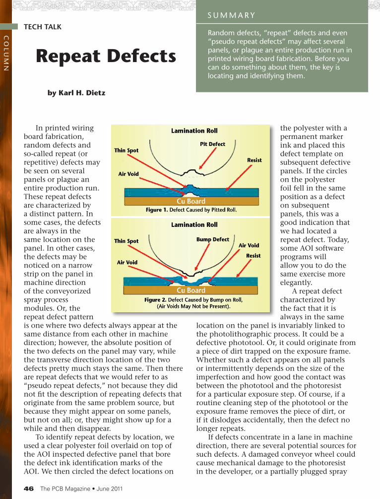
46 The PCB Magazine • June 2011
Repeat Defects
by karl H. Dietz
random defects, “repeat” defects and even “pseudo repeat defects” may affect several panels, or plague an entire production run in printed wiring board fabrication. before you can do something about them, the key is locating and identifying them.
s u m m a r YTeCH TALk
co
lu
mn
In printed wiring board fabrication, random defects and so-called repeat (or repetitive) defects may be seen on several panels or plague an entire production run. These repeat defects are characterized by a distinct pattern. In some cases, the defects are always in the same location on the panel. In other cases, the defects may be noticed on a narrow strip on the panel in machine direction of the conveyorized spray process modules. Or, the repeat defect pattern is one where two defects always appear at the same distance from each other in machine direction; however, the absolute position of the two defects on the panel may vary, while the transverse direction location of the two defects pretty much stays the same. Then there are repeat defects that we would refer to as “pseudo repeat defects,” not because they did not fit the description of repeating defects that originate from the same problem source, but because they might appear on some panels, but not on all; or, they might show up for a while and then disappear.
To identify repeat defects by location, we used a clear polyester foil overlaid on top of the AOI inspected defective panel that bore the defect ink identification marks of the AOI. We then circled the defect locations on
the polyester with a permanent marker ink and placed this defect template on subsequent defective panels. If the circles on the polyester foil fell in the same position as a defect on subsequent panels, this was a good indication that we had located a repeat defect. Today, some AOI software programs will allow you to do the same exercise more elegantly.
A repeat defect characterized by the fact that it is always in the same
location on the panel is invariably linked to the photolithographic process. It could be a defective phototool. Or, it could originate from a piece of dirt trapped on the exposure frame. Whether such a defect appears on all panels or intermittently depends on the size of the imperfection and how good the contact was between the phototool and the photoresist for a particular exposure step. Of course, if a routine cleaning step of the phototool or the exposure frame removes the piece of dirt, or if it dislodges accidentally, then the defect no longer repeats.
If defects concentrate in a lane in machine direction, there are several potential sources for such defects. A damaged conveyor wheel could cause mechanical damage to the photoresist in the developer, or a partially plugged spray
48 The PCB Magazine • June 2011
REPEAT DEFECTS continues
nozzle can cause highly localized, high-pressure spray impact in the developer or etcher resulting in over-development or over-etching.
Repeat defects related to hot roll lamination have two causes: either by a pit, indentation or cut in the rubber cover of the roll, or by a bump on the roll resulting from a nodule of foreign material on the otherwise smooth roll surface (see Figures 1 and 2 ).
A pit on the roll surface causes inadequate lamination pressure, which can cause an air void or low dry film adhesion that will not survive the rest of the process (see Figure 1). Bumps on the roll are usually caused by resist contamination. Such bumps increase lamination pressure, causing resist thinning. Such thin resist may not survive downstream processing. A thick bump with steep sidewalls may cause air voids or low adhesion around the edge of the bump as well as resist thinning (see Figure 2). Both types of roll defects will cause opens or nicks in etching applications, and shorts or excess copper in pattern plate applications.
Repetitive lamination voids can easily be detected. Most appear as light spots on laminated boards due to air under the resist. Thin resist spots without air voids are seen
as dimples in the resist when observed at an angle. All defects caused by lamination rolls will repeat at the distance equal to the circumference of the roll. Note that, due to the spacing between boards, defects may not appear at the same location on each board.
Bumps on the lamination rolls caused by resist contamination can usually be removed by cleaning with isopropyl alcohol (caution: it’s flammable!). Problems caused by pits on the lamination rolls can be corrected permanently only by replacing the rolls. Some vendors offer repaired (recovered) rolls as a less costly alternative. Temporary repairs by filling the pits with a high temperature silicone adhesive sealant are possible, but they may fail within days because of thermal cycling. PCB
Karl dietz is president of Karl dietz consulting, llc. He is offering consulting services and tutorials in the field of circuit board & substrate fabrication technology. Karl can be reached by e-mail
at [email protected] or phone (001) 919 870 6230.
sH
or
t
gRAPHIC PLC ReCeIveS AWARD FRoM BAe SYSTeMSGraphic plc of devon, england has
received a special “supplier recognition award” from bae systems. the award recognizes Graphic’s on-time delivery, Quality and support performance for the past 12 months to bae systems.
this is the third such award received from Graphic’s major oem customers in the past six months, and shows the company’s commitment to world class manufacturing performance at the highest level. Graphic plc is involved with the sc21 program and has achieved as9100 and nadcap amongst other international business Quality awards.
About Graphic PLC Graphic plc is one of the most technically-
competent manufacturers of high-technology pcbs. located in the heart of the english countryside, Graphic focuses on leading-edge technology released to the most demanding international quality standards. constantly looking at innovative solutions to customer requirements, Graphic is an expert at prototyping and developing new “first-to-market” products. With facilities in the uK and in china for medium- to large-volume production, Graphic is able to offer complete services for pcb manufacturing.

June 2011 • The PCB Magazine 49
When Honeywell aerospace writes contracts with suppliers and subcontractors, it relies on ipc docu-ments to establish many details.
language barriers occur just as regularly when technologists in one discipline communicate as they do when people from different countries talk to each other. in the technical world, standards help alleviate these misunderstandings, making it much easier for companies that work with suppliers and subcontrac-tors.
large companies that deal with more outsiders—and have more insiders who work in many disparate disciplines—often make extensive use of standards in order to reduce the number of mistakes that can and will arise.
Guidelines by standards bodies such as ipc are used throughout the relationship between companies. Good documentation can help companies forge strong relationships from the start, ensuring that a supplier or subcontractor can meet the requirements of an oem.
“When we’re looking for new suppliers or partners, we need a way to look at their technical capabilities. if they can say that they’re able to build printed boards or printed board assemblies to the relevant class 3 ipc require-ments, it gives us a lot more confidence that they will be able to fulfill a production run,” said dewey Whit-taker, staff engineer at Honeywell aerospace.
one of the most important aspects of standards and guidelines is that they define the terms in un-ambiguous language. many technical terms mean different things to people in different disciplines, so they need to be defined for communication that goes outside a single group.
“some of the things set in ipc documents sound simplistic, but you need universal agreement for what the term “eight” means. not that “eight” is acceptable to everyone, but that it is understood by everyone be-fore you can move forward,” Whittaker said, only half in jest. He added that it’s always important to ensure that what seems apparent to one side is also apparent to the other.
this move to standardization helps foster good relationships between companies by reducing the ag-gravation that occurs when one party doesn’t view an issue in the same way as the other. many times, one party will think everything is fine until managers at the other company are upset about problems.
“in the past, if you had a problem you could spend a week going through white board discussions just trying to get commitment that a problem is a problem. that’s very frustrating,” Whittaker said.
With a standard, it’s very clear whether or not the requirements were met. “data is data, there’s no longer any language barrier,” Whittaker said. “using a standard hopefully ensures that you understood what was meant and that you can do what the standard says.”
Whittaker is a big proponent of standards, but he noted that no document will ever ensure that confu-sion won’t rear its ugly head. While standards can reduce the likelihood of misunderstandings, nothing can eliminate miscommunication when people are involved. “We’ve worked with companies that look at all our requirements, things like building ipc-6012 class 3 printed boards with varying types of vias and reviewed by staffers that have gone through ipc-cer-tified training programs and said yes to all of them. then we find that they don’t necessarily have plans to use all those capabilities nor understand that it is a mandate of ours to invoke all those requirements when they produce our printed boards. it’s flabber-gasting, but it happens,” Whittaker said.
though these types of problems can occur, they’re thankfully rare. providing a common base of understand-ing is a huge step for companies that are attempting to work
with a growing number of subcontractors. However, many guidelines give companies some flexibility in the way they do things. that openness may not be effective for a company that’s setting guidelines for a contract. nonetheless, the guidelines can be tweaked by simply telling the subcontractor where minor changes must be made.
“When you start outsourcing, you have to be very clear,” Whittaker said. “that can create some huge documents. but i can keep them short by saying they must meet ipc-6012 class 3 or 3/a acceptance criteria with some exceptions/deviations. i replace will with shall, so they have to do those things,” Whit-taker said.
though standards aren’t designed to boost a country’s self-esteem or its standing in the world, they can help emerging nations step forward. cor-porations in these nations can use standards to show that they match the capabilities of more experienced companies in countries that have been industrialized for longer periods. When these companies in emerg-ing nations bring in business from top-tier providers, the entire country benefits.
“a standard breaks down the barriers, chang-ing how companies in different countries rank and view themselves,” Whittaker said. “in many emerg-ing countries, there’s a lot of prestige and honor by having a major corporation have a presence in their country.”
Honeywell Relies on Standards to Set Contractor Expectationss
Ho
rt
by Terry Costlow
June 2011 • The PCB Magazine 49

50 The PCB Magazine • June 2011
How to Implement Lean Manufacturing into a Printed Circuit Board Shop
Part 2: Common Questions
by Dale Smith
part 2 of this five-part series on implementing lean manufacturing into a pcb shop, columnist dale smith unravels the common questions surrounding the issue: What are the excuses? What are the wastes? What are my expectations?
s u m m a r YTHe LeAN MeAN PCB SPeCIALIST
co
lu
mn
There are more, but quite frankly, they too are just excuses. Lean Manufacturing is about removing waste. Removing waste is a good thing no matter what is being produced! You can “Lean Out” your garage or basement. Have you ever looked for tools that you know you own, but can’t find? A half-hour job ends up taking all afternoon because you couldn’t find the tools. What a waste of time! You probably could have completed several more tasks in
that time period. This is just an example of how improved efficiencies can reduce cost and cycle time (two or three tasks completed in an afternoon instead of one, and a single task completed in thirty minutes).
In a PCB shop, most people think waste is scrap and rework. Yes, these are important wastes to eliminate or reduce, but there are other types of waste that nobody considers which are just as important.
Here are a few common reasons cited by companies who do not implement Lean:
In General:1. We are a small company. We don’t have the resources that bigger companies have and we can’t afford it.2. We’re too busy. We don’t have time to make changes or to train.3. We don’t have highly skilled factory operators. We have a hard time just getting them to follow procedures, and you want us to empower them?4. Fear factor. We are afraid to make changes; we don’t want to make things worse.5. We don’t know how to implement. Where do we begin? 6. We would consider asking for help, but outside instructors don’t understand our business.
Specific to the PCB industry:1. We manufacture a custom product. it’s different all the time.2. We manufacture many different product types, with varying numbers of process steps. 3. our product is highly complex and technical.4. We have product that requires a flow back to a previous operation.5. We only build prototypes. a part number may only be manufactured one time. 6. We have many “new” part numbers that we have never built before.7. We build prototypes and volume production quantities in the same facility; therefore, there is a demand conflict. the prototype work needs to be processed immediately, causing the “production” work to suffer delivery issues (or vice-versa).8. We do not have much automated equipment.

Why choose Fein-Line?Because there is a Fine Line between winning ...and the alternative.
After more than 44 years in the industry, just about everyone knows the name Dan (Baer) Feinberg.
There are few in our industry that have his experience and expertise in just about every aspect of the business. Dan knows what works, and perhaps more importantly, what doesn’t.
When additional expertise is needed, or when senior management just needs an independent opinion, companies large and small alike get the guidance of Fein-Line Associates, especially in the areas of New Product Market Entry and M&A Due Diligence.
In our business, there's a lot on the line, not just sometimes, but every time. The line between success and the alternative can be razor thin. That’s why winning companies choose Fein-Line time after time.
Sales Training General Marketing Assistance · New Product Market EntryMerger and Acquisition Due Diligence · Printed Circuit Technology assessment
Market Research (It may work but will it sell) · Expert Witness assignmentsTechnology Transfer
Fein-Line Associates, Inc.P.O. Box 73355, San Clemente, CA 92673-0112
(949) 498-7866
www.feinline.com
Dan (Baer) FeinbergFein-Line Associates

52 The PCB Magazine • June 2011
What is “waste” in a manufacturing operation?
Waste: Any activity which utilizes equipment, materials, parts, space, employee time or other resources beyond the minimum amount required for value-added operations to ensure manufacturability. These situations should be considered as opportunities for improvement. Ideally, we only want to be performing tasks that the customer will pay for (you will see the importance of this statement in later commentary). More specifically, waste activities are as follows:
1. Overproduction (producing more product than the customer needs)2. Delays (any time when value is not being added to the product)3. Transporting of materials from process to process4. Over-processing (doing more work than required to meet customer requirements)5. Inventory (WIP and storage)6. Motion (moving product more than required to manufacture)7. Scrap and Rework8. Lack of Innovation (failure to encourage new ideas or develop better methods)
If I eliminate or reduce these wastes, what results could I expect to gain?
We are not talking about gains of three, five or 10%. I have seen companies gain over 50% in their productivity output! Some companies have reduced their lead times by over 60%! On top of these gains, some have realized reduction in WIP by as much as 30%.
However, success depends on the effort and commitment to the principles. Companies who only commit limited time and/or resources, and are unwilling to make changes (which can be significant), will not realize much improvement for their efforts. Companies that believe in the principles and
make the commitment with focused efforts on waste reduction can experience the substantial types of gains mentioned above.
How quickly would I expect to see results?Again, results would depend upon the
effort. From my experience, the expectation would be to begin seeing results in about three to six months. Initially, there needs to be an intense focus on training. For this to occur, upper management must “buy in.” Management must be committed to the principles and have a basic understanding of them. It’s fine to have some doubts, but management must believe that the program is good for the company and, once implemented, will yield results. Management also needs to understand what is required of them, specifically. It is helpful to have a “Lean Road Map” outlining the path forward with an estimated timeline to complete the tasks. Therefore, it is extremely important to have one or more experienced Lean Coordinators to advise and guide the company through the process. Don’t forget—you are talking about changing the culture of the company! It must be implemented carefully or pessimism will grow and try to defeat the effort. To get the
program off on the right foot, get some positive results early, and build on that momentum.
What are the costs?There are some costs
to consider. Consultant(s) hired for guiding/advising must have their fees budgeted. Time must be allotted for company associates to be trained
(work will not be performed during these sessions). As you progress further into implementation, it may be advantageous to move equipment, re-organize work areas or add resources. This should be weighed and analyzed to ensure that the investment brings rewards. After all, you don’t want to spend $20k for a $10k return, or wait for returns that will not pay back for many years. It is
LEAN MANUFACTURING, PART 2: COMMON QUESTIONS continues
“ it is helPfUl to have a
“lean road maP” oUtlining the Path forWard With an
estimated timeline to comPlete
the tasks. ”

Your Single Source for Your Electrical Test Needs
LM800 PicomatGrid test with Sniper optical board alignment
A5aFully automatic flying probe test system
S2High speed Flying probe test system
atg Luther & Maelzer is a leading supplier of electrical testing solutions for the pcb industry. We offer solutions for every application ranging from main stream technology all the way to HDI products such as smart phones and tablet PC technology. Our atg flying probe tester products are renowned for speed, accuracy and automation while the Luther & Maelzer grid tester product range is known world wide for high throughput, repeatability and flexibility.
www.atg-lm.comPhone: +49 (9342) 291-0E-mail: sales@ atg-lm.com

54 The PCB Magazine • June 2011
also more difficult to qualify the returns of some investments. For example, if we don’t reduce our lead times, we may never get the opportunity to win business from a potential customer because we cannot meet their needs. How do you put a price on that? Usually these types of decisions are obvious. Having a long-range plan will be important, but it’s too early to worry about now. You don’t have enough data yet to understand what the needs will be. This will be discussed in subsequent columns.
Do I have a capable management staff?Good question! Moreover, an important
one! Lean is not complicated; it’s mostly common sense. Obviously, a strong staff is critical for achieving success in any organization or implementing a new program. My experience is that most companies have a capable staff. Most have the skills that are necessary for planning, implementing and executing. The staff should be able to challenge the status quo, focus on continuous improvement (removing waste) and build on the positive results. Further, you want to develop this culture throughout the entire organization, so it is important that the team listen to all concerns in order to avoid making rash decisions that could lead to mistakes affecting performance or quality. Two important questions for you to consider are:
1. Can management work together as a team?2. Will the team apply the necessary effort for planning, implementing, executing and sustaining the program?
Do I have capable manufacturing associates?
My experience is that most companies’ manufacturing associates (supervision and operators) have adequate skills to adopt the new principles. I find they are mostly willing to participate in the improvement process. In fact, many find that for the first time, the company is listening to them. What a revelation! This is exactly what you will be encouraging.
Again, do not underestimate the
importance of listening to all concerns to avoid decisions that could negatively affect performance or quality.
Can lean fail?Yes!The main reason for failure typically lies
in upper management. If upper management sings from the same song sheet, that is, demonstrates commitment, focus and agreement with the plan, the rest of the organization will usually follow along. As within any organizational structure, if individual(s) are not committed to the program, it can cause impediment to the planning, implementation or execution. Ultimately, this could affect results or cause delays.
Here are a few of the reasons why Lean fails, or is not nearly as effective:
• No “buy in,” or misunderstanding of the principles• No priority status and therefore no focus • Lack of clearly defined objectives/goals• Belief that the effort should be delegated• Inability to work together as a management team• Absence of a plan for implementation or execution
Now we have some understanding of what Lean Manufacturing is all about and what the expectations are for implementing the program. We have some reasons to get excited! In Part 3, we will discuss key customer values that will help keep us focused. PCB
dale a. smith is president of das Flex circuit consultant and has more 30 years experience in the printed circuit industry. He specializes in rigid/Flex high reliability manufacturing and lean
manufacturing implementation into pcb shops. reach dale at 267-424-0690 or email [email protected].
LEAN MANUFACTURING, PART 2: COMMON QUESTIONS continues

June 2011 • The PCB Magazine 55
sH
or
t
multiple research and development agreements have been signed by atotech and case Western reserve university (cWru) for the support and enhancement of atotech’s global metallization technology development and material science and application failure analysis activities in europe, asia and the u.s.
the established agreements with the department of materials science and engineering, as well as with the institute of advanced materials, will further strengthen atotech’s chemistry and analytical capabilities. atotech’s potential is catalyzed by the 16 global technology centers, which include the semiconductor chemistry r&d and application center at the college of nano-scale science and engineering (cnse) in albany, new York.
each technology center site is responsible for supporting local and international development and optimization activities of plating chemistries for tailored regional processes and applications.
the department of materials science and engineering at case Western reserve university supports nano-scale inspections, as well as failure and property analysis that include trace element analytics with high-resolution instruments.
the collaborative agreement includes the establishment of an organic chemistry laboratory dedicated to the support of new plating additive development that is specialized for small scale, feature-size plating. the laboratory will further enable and enhance atotech’s semiconductor r&d activities, which focus primarily on the optimization of copper plating process solutions using advanced polymers for structures down to the 22 nm node. additional research is being performed on plating process development for sub-22 nm node structures.
the new organic laboratory focuses on the physical treatment of existing organic polymers
Atotech to enhAnce technology; collAborAte with cwrU
as well as on the development of new polymers. these organic additives play a major role in defect-free bottom-up fill technologies of copper damascene structures, which are critical for the chip’s wiring from m1 up to mx copper layers. these polymers must be optimized to fulfill the requirements for scaled barrier liner, seed layers or for direct plating on liner layers in advanced structures.
Wide process windows are needed to plate semiconductor metal structures in various types of equipment, especially when dealing with a vast range of structure sizes from the nano-scale to the micro-scale.
the same plating bath chemistry must perform uniformly across the wafer. as structures are sensitive to contamination, leading to a risk of yield losses or reliability exposures, the
target is to achieve low incorporation levels of organics or organic by-products. minimizing the consumption rate over the throughput in an ecd plating tool is also a goal.
atotech’s Vice president of semiconductor technology, robert
preisser, stated after signing the contracts that he is very pleased with the new agreements between case Western reserve university and atotech.
“this new collaboration addresses open activities that will support r&d for nano scale metallization chemistry and process development. this collaboration is a strategic continuation of the existing cooperation between electrochemical research group at case Western reserve’s department of chemical engineering and atotech.”
professor uziel landau, chair of the chemical engineering department and a long-time research collaborator of atotech states that he is delighted with the progress made so far under the sponsorship of atotech in advancing the state of interconnect plating technology, and looks forward to the enhanced collaboration.
June 2011 • The PCB Magazine 55

56 The PCB Magazine • June 2011
Microvia Separation
by Paul ReidpWb interconnect solutions
microvias can fail in many ways, but by far the most common is a separation between the base of the microvia and the target pad. Frequently, the separation is below the electroless copper or direct metallization layer and the target pad. the challenge is cleaning organic residues off the base of the microvia.
s u m m a r YReID oN ReLIABILITY
co
lu
mn
Microvias are best described as small blind vias. They usually have a diameter of .004” to .006” or less, and aspect ratios are frequently in the range of, but by no means limited to, between 1:1 and 3:1. Although the microvia has a relatively modest aspect ratio, as compared to HDI boards with plated through vias, they are a challenge to fabricate, mostly due their small size.
Of all the interconnect structures, well-made microvias consistently outperform all other interconnect types based on thermal cycle testing. At the same time, poorly fabricated microvias fail catastrophically in assembly and in the end-use environment. Conventional test methods like solder float and thermal cycle testing at 150°C have been known to produce false-positive results on marginal microvias that subsequently failed in assembly.
The anatomy of a microvia includes a capture pad through which a hole is drilled or ablated, the target pad at which the hole terminates and the sides of the hole walls, or barrel of the microvia. The microvia may be open or filled with epoxy or copper, and may or may not have a copper cap. Usually the microvia is penetrating approximately .003” or .004” of the dielectric. Microvias are frequently found in sequential lamination applications.
Microvias are very small. As a means of comparison I have fine hair which is rather thin, measuring about .002”. Two or three of my hairs would fit side by side inside a microvia. Surface tension, viscosity, wetting and the small size of the opening makes it difficult for fresh chemistries to get into a microvia and for spent
chemistries to be replaced. For the purpose of this article, and
based on reliability testing, we can place microvias into two distinct groups: simple and compound. Simple structures are microvias that are not stacked on top of either other microvias or buried vias. Compound microvias are defined as those microvias that are directly stacked on top of other microvias or buried vias. Simple microvias may span one or more dielectric layers, but tend to be floating with dielectric material directly below. Stacked microvia connect directly on top of other copper interconnections.
Usually, we find a simple microvia between other interconnect structures like plated through holes (PTHs). During a thermal excursion, if a microvia is between two adjacent PTHs, the PTHs will act like rivets, constraining the z-axis expansion. Dielectric material will expand, bulging out between PTHs, pushing the microvia structure upward (or down) as it floats on a bed of expanding dielectric. The microvia, because of its
Figure 1: anatomy of a microvia.

IPC InternatIonal ConferenCe on flexIble CIrCuIts WorkshoPs June 21teChnICal ConferenCe June 22–23Minneapolis, Minn.PartICIPate In the groWth of the flex CIrCuIt Industry!
•DiscoverflexopportunitiesandchallengesasseenbyPrismarkPartners
•HearfromRIM,Delphi,MayoClinicandLockheedMartinontheirrequirementsforflexboards
•LearnthelatestdevelopmentsinflexmaterialsfromDuPont,ArlonandTapco
•Discoverbestmethodsforsolvingprocessingissues
•ReceiveperformancereliabilitydatafromRockwellCollins
•LearnwhatthelatestIPCstudiesrevealsabouttheflexmarket
seleCt froM three In-dePth WorkshoPs taught by flex CIrCuIt exPerts:•PrimerforFlexFabrication,instructorMarkVerbrugge,leadapplicationsengineer,MincoProducts
•SpecialConsiderationsinFlex/RigidFlex,instructorGregBartlett,generalmanager,VulcanFlexCircuitCorp.
•DesignforManufacture:OptionsforOptimumManufacturingReliability,instructorTomGardeski,president,GeminiSciences,LLC
To learn more and to register, visit www.ipc.org/flexible-circuits.
Getyourmessagetothiskeyaudiencewithatabletopexhibitorsponsorship!
Formoreinformationabouthowsponsorshipsenhanceyourmarketingefforts,[email protected]+1847-597-2866.

58 The PCB Magazine • June 2011
diminutive size, experiences pad rotation downward (toward the center of the board) during the thermal excursion.
In 2004, a cooperative study that included Paul Andrews (Curtiss Wright), Gareth Parry (Coretec) and the team at PWB Interconnect Solutions demonstrated that known compromised microvias (microvias that failed in assembly) had survived to the end of 1,000 test cycles that tested to 150°C. The associated boards had an approximate 30% failure rate in tin/lead assembly. That case study demonstrated that testing microvias at 190°C causes known compromised microvias to fail in less than 500 cycles without inducing artifact failure modes. The findings from that study set the standard for the 190°C testing of microvias that continues today.
It appears that microvias need to be near or above Tg in order to produce enough stress to break weak microvias—microvias that will fail in tin/lead assembly and rework. These
findings, with microvias tested at 190°C, have been reiterated many times over the years in studies and practical applications. The effectiveness of 190°C testing of microvias has been repeatedly reinforced with unexpected assembly and field failures as a result of companies testing at 150°C.
There are many ways microvias can fail, but by far the most common is a separation between the base of the microvia and the target pad. Frequently, the separation is below the electroless copper or direct metallization layer and the target pad. The challenge is cleaning organic residues off the base of the microvia. The residue from laser ablation coats the walls and the base of the microvia and acts as a protective coating, resisting cleaning and microetching of the target pad. The contaminating residue is often not visible using optical microscopy. The presence of residue is inferred when the target pad is not visibly etched by the microetch bath.
By comparing the degree of etch at the base of the microvia to, say, an interconnection in the PTH that is being cleaned at the same time as the base of the microvia, one can determine whether the residue in the microvia has been removed or is still present and resisting adequate etching. Generally robust microvia show evidence of some degree of etching at the target pad. Undoubtedly, evidence of microetch is not required for a microvia to be robust, but, when present, it offers visible evidence that cleaning has been adequate.
By using thermal cycle testing to study robustness of microvias, we can plot the resistance change throughout the thermal excursion and determine when failure (a 10% increase in resistance) occurs. Microvias that fail due to a separation to the target pad tend to fail catastrophically in just a few cycles after
MICROVIA SEPARATION continues
Figure 2: Forces acting on a microvia.
IST Thermal Cycles to Failure –
Preconditioned 5 X 2300C
test temperature 150c 170c 190c 210c 220c
mean ist cycles 1000 789 464 76 44
Table 1: cycle-to-failure data on compromised microvias at various temperatures.

60 The PCB Magazine • June 2011
onset. Based on how microvias fail during thermal cycle testing, the animation in Figure 4 has been drawn to show a crack at the base of the microvia; the crack is induced in the heating cycle and then opens in the cooling, only to close again at ambient.
Note that the animation shows a microvia that floats on a base of dielectric without another interconnect structure in the near vicinity. Because the microvia is floating on a base of dielectric, the pad rotation is down (or up) toward the center zone of the board. Small inclusions and cracks coalesce into a large crack in the heating cycle. Cracks that close at ambient, presenting little or no increase in resistance at ambient, may be described as self-healing between thermal excursions. Microvias that fail due to microvia-to-target pad separation frequently exhibit intermittent opens that are hard to find in failed product.
Although microvias are demonstrated to be the most robust interconnect structures when fabricated
correctly, most companies evolve their processes to achieve that result. The learning curve is sometimes steep and occurs over too long a time. In the interim, failures may be expected. Thermal cycle testing is a perfect tool for the fabricator to hone their process and can significantly reduce time to results by producing objective evidence to rank the effects of process changes. When tested at 190°C, thermal cycle results from microvia testing is objective evidence of capability for potential customers. PCB
MICROVIA SEPARATION continues
Figure 3: still shot from animation showing microvia separation. click here for animation.
paul reid is a program coordinator at pWb interconnect solutions inc., ottawa, where his duties include reliability testing, failure analysis material analysis and pWb reliability consulting.
contact paul reid at [email protected] 4: microvia separation.

62 The PCB Magazine • June 2011
a Black Pad & Brittle Fracture: Controlling the ENIG Process
Michael Carano of OMG Electronic Chemicals is well aware that the use of ENIG poses quite a few challenges, but millions of dollars worth of PCBs are successfully produced on a monthly basis using ENIG. It is critical to review the ENIG process and set the stage for success.
b Do You know Your PTH from a Hole in the Ground?
Regardless of your score on this quiz, you will be a hero to your product managers and assemblers if you design your PTHs with the proper thermal relief and ground plane locations. Trust us, we’re Geeks.
c APEX Honors Best Industry Posters, Competition Winners
Celebrating the best of electronic interconnec-tion research being conducted by both industry leaders and academia, IPC announced the 2011 Best Industry Posters, and the winners of the IPC Academic Poster Competition at IPC APEX Expo, held April 12-14, 2011, in Las Vegas, Nevada.
d The Way I See It: Prophet of Doom, Again!
Physicist Michio Kaku has written a book, “The Physics of the Future,” which takes my angst about the demise of the PCB up a couple of notches. Kaku forecasts the demise of Moore’s Law and says how it will end, and what replaces it, depends on the laws of physics. The answers to these physics questions will eventually rock the economic structure of capitalism.
Top TenMost-Read News Highlights from PCB007 this Month
62 The PCB Magazine • June 2011
ne
Ws

June 2011 • The PCB Magazine 63
e John Ling Reviews IEEE Workshop on Reliability and Safety
A thoroughly worthwhile event held within the magnificent buildings of the University of Greenwich, comprising a thoughtful programme of papers from a wide variety of speakers, all of whom held to the one theme announced in the banner—reliability and safety.
f It’s Only Common Sense: Is the U.S. the New China? I read recently that the Swedish furniture and household goods giant IKEA is moving their operations out of Sweden. In fact, they’re moving their operations out of Europe completely.
g I-Connect007 Launches Free Flex Video Series
I-Connect007 has launched the “Flexible Circuit Technology Online Training Video Series.” Divided into nine sessions, this first-of-its-kind video series is a companion to Joe Fjelstad’s exhaustive book, “Flexible Circuits Technology.” Welcome to learning on demand, on your schedule!
h PCB Imaging & Registration Focus of EIPC Seminar
EIPC Executive Director Dr. Konrad Wundt introduced an outstanding program of presentations that provided PCB fabricators with state-of-the-art knowledge, addressing the realities of tolerances and registration to enable the improvement of manufacturing yields, and to understand what could be achieved with the latest developments.
i APEX: Record Donations for Japanese Red Cross
Betting on the generosity of the electronics industry gathered at IPC APEX Expo recently in Las Vegas, Nevada, IPC held a raffle to raise funds for the Japan relief fund of the Red Cross. A total of $4,195 was raised from the raffle with 100% of the proceeds going to the Japanese Red Cross.
j It’s Only Common Sense: Make Your Company Famous
PCB companies are now ready to let people know who they are and what they are doing. This week, Dan Beaulieu offers six easy and, yes, economical ways to make your company famous.
Most-Read News Highlights from PCB007 this Month
June 2011 • The PCB Magazine 63
64 The PCB Magazine • June 2011
• IPC Complete Calendar of Events
• SMTA Calendar of Events
• iNEMI Calendar
• PCB007 Events
MILESTONE June 2011Baltimore, New England, Los Angeles
Space Coast Chapter Expo, Technical Forum and BarbequeJune 9, 2011Melbourne Auditorium, Melbourne, Florida IPC Summit on American CompetitivenessJune 15 - 16, 2011Washington, D.C. IPC International Conference on Flexible CircuitsJune 21 - 23, 2011Minneapolis, Minnesota, USA Energy Harvesting & Storage Europe 2011June 21 - 22, 2011Munich, Germany Wireless Sensor Networks & RTLS Europe 2011June 21 - 22, 2011Munich, Germany
Nepcon ThailandJun 23 - 26, 2011Bitec, Bangkok, Thailand Assembly Technology 2011June 23 - 26, 2011BITEC, Bangkok, Thailand LEDforum Shanghai 2011 July 6 - 7, 2011Jumeirah Himalayas Hotel Shanghai, 1108 Meihua Road, Pudong Xinqu
ca
le
nd
ar
eveNTS
64 The PCB Magazine • June 2011

IPC Summit on American Competitiveness
Washington, D.C. | June 15–16, 2011
Combining Capitol Hill Day with a conference focused on the needs of the U.S. electronics industry
THE IPC SUMMIT ON AMERICAN COMPETITIVENESS combines informative presentations, legislative and regulatory briefings and key lobbying visits with members of Congress to discuss critical issues that impact the U.S. electronics industry’s ability to compete globally.
LEARN HOW YOUR COMPANY CAN INCREASE ITS COMPETITIVENESS • Discover what technologies represent the best chance for your company’s success as a U.S. electronics manufacturer. • Hear how other U.S. electronics manufacturing companies are ensuring their competitiveness. •Find out how you can use government resources to strengthen your business.
MEET WITH YOUR MEMBERS OF CONGRESS ON CRITICAL ISSUES THAT IMPACT YOUR BUSINESS
•Electronicscompaniesthroughoutthesupplychainwillbeencumberedwithsignificant costs and burdensome reporting requirements for conflict minerals.
•CongressionalactionsandinactionswillaffectthefutureabilityoftheNorthAmericanelectronics industry to meet military and aerospace needs.
•Legislatorsneedtohearabouttheconsequencesontheelectronicssupplychainof over-regulation.
IPC will make lobbying easy for you by briefing you on the legislative issues and giving you the necessary materials. IPC will arrange your congressional appointments before you arrive, making your experience smooth and efficient. Your participation will help you build a beneficial relationship with your elected officials.
PARTICIPATE IN SPECIAL FUNCTIONS WITH MEMBERS OF THE NATIONAL ASSOCIATION OF MANUFACTURERS •HeardirectlyfromMembersofCongressandseniorleveladministrationofficialsduring
two special presentations. •Networkatareceptionwithmorethan350U.S.manufacturingexecutives.
Learn more and register today at www.IPC.org/CHD.

66 The PCB Magazine • June 2011
Chinaby Barry Matties
the rush to establish a presence in china has hit a snag; that is, the country may be full. after several years of companies scrambling to seek out and secure partnerships, and open offices, not to mention navigate the cultural differences, the dust has settled, and the supply base has been established. that was our impression recently after attending nepcon china and circuitex.
s u m m a r YTHe SALeS CYCLe
co
lu
mn
I recently spent a few weeks in China attending a two trade shows, NEPCON China and Circuitex. Organized by the Reed group, NEPCON focuses primarily on the assembly market, while Circuitex is mainly a PCB fabrication event. Circuitex, organized by the Taiwanese Printed Circuit Association, takes place in Suzhou, about an hour from Shanghai. One thing that was clear at both shows is the rush to get to China is well past; the supply base has been established.
Not too many years ago, companies were rushing to navigate the cultural difference and the language barriers, searching to set up partnerships, open offices and just trying to figure out how to conduct business in China. Well, the dust has settled and if you are doing business in China, great. If you aren’t, it may be too late. I spoke with a few of the PCB suppliers that have been in China for several years. They reported that their business is great, for the moment. In fact, several suppliers said they could not take any
more orders for the year; they just don’t have capacity to handle all that they currently have. From wet processing to inspection, no one seems to be complaining. But a few I talked with are concerned that next year might be considerably slower as the pent-up demand for equipment is being satisfied this year.
More than just suppliers have made the jump into the China market; IPC has also developed a strong presence there. They are still busy hiring new people, opening offices and training the industry. Many, over the years, have been critical of IPC for this effort, but in the end, they are a business like all others, vulnerable to market conditions. In business, no matter what type, market conditions will always have an influence, and you can either adapt or disappear. IPC has definitely adapted; in fact, some there have said, in the coming years, they expect to have more employees in China than they do in the U.S. I don’t find that surprising. All you have to do is visit a trade show there to gain

68 The PCB Magazine • June 2011
CHINA continues
an understanding of this. IPC’s board did just that by holding its annual meeting at the recent CPCA show in Shanghai.
If you would like to learn more about IPC’s global strategy, check out this video: IPC Video.
I still experience moments in China that make me wonder how anything gets done. Sometimes it just seems that logic escapes their thought process (if you have spent any time there you clearly understand what I mean), yet they continue to grow. Maybe that lack of logic is residual from the old China, because the new China strategy is focused on competing on a worldwide level, with a strong desire to become the world’s superpower. With 1.6 billion people and a thriving economy, they seem to be on that path. I have never seen as many Ferrari dealerships in one city as I have in Shanghai. Not only are the dealers there, but there are plenty of Ferraris, Lamborghinis, Aston Martins and other high-end cars on the road. Their wealth continues to be explosive.
We often hire helpers in China to assist us in our trade show coverage effort. They help with the camera, running errands and providing security in our booth against thieves. Yes, there are plenty of thieves. In fact, during this visit, my rented bicycle was stolen. When I shared the story with some of our Chinese friends, none were surprised. As it turns out, most have had their bikes stolen at one point or another.
Education is clearly one noticeable difference between China and the U.S. The helper we hired for extra security was only a few credits away from becoming a Ph.D. As many of our kids graduate from high school,
it is very sad to say that many cannot even point out China on a map. Many that do go to college for a degree are graduating now only to find jobs at fast food restaurants, supermarkets, etc. When I look at our industry, I do not see many young people coming into it. It seems to me that part of our competitive advantage, as a nation, lies within a higher educational level. Certainly, China understands this concept and so does the IPC, hence their growth in China.
If you have not yet been to China, I recommend that you plan a trip to see for yourself what all the buzz is about. Visit a trade show, a factory and some of the suppliers. I think you will be amazed and it will give you a greater appreciation for the global economy. PCB
barry matties started in pcb manufacturing in the early 1980s. in 1987, he co-founded Circuitree Magazine. nearly 13 years later, Circuitree was sold
as the leading publication in the industry. in the early 2000s barry and his former Cir-cuitree partner, ray rasmussen, joined forces again and acquired pcb007. over the years, pcb007 has grown and continues to thrive. in July of last year, barry and ray acquired SMt Magazine. With his many years of business leadership skills, barry now produces this col-umn for anyone who has a desire for success. the column relates 25 years of successful business leadership, including marketing and selling strategies that really work. read a few and decide for yourself.

June 2011 • The PCB Magazine 69
publisHer: BARRY [email protected]
publisHer: RAY RASMUSSEN(916) 294-7147; [email protected]
sales: ANGELA ALEXANDER (408) 915-2198; [email protected]
eDItoRIAL:Group editorial director: RAY RASMUSSEN(916) 294-7147; [email protected]
manaGinG editor: LISA LUCkE(209) 304-4011; [email protected]
tecHnical editor: PETE STARkEY+44 (0) 1455 293333; [email protected]
MAGAZINe PRoDUCtIoN CReW:
production manaGer: MIkE RADOGNA [email protected]
MAGAZINE LAYOUT: RON MEOGROSSI
ad desiGn: MIkE RADOGNA, BRYSON MATTIES,
SHELLY STEIN
innoVatiVe tecHnoloGY: BRYSON MATTIES
coVer: MIkE RADOGNA, BRYSON MATTIES
the pcb magazine® is published by br publishing, inc., po box 50, seaside, or 97138
©2011 br publishing, inc. does not assume and hereby disclaims any liability to any person for loss or damage caused by errors or omissions in the material contained within this publication, regardless of whether such errors or omissions are caused accidentally, from negligence or any other cause.
June 2011, Volume 1, Number 2 • The PCB Magazine© is published monthly, by BR Publishing, Inc.
AD INDex Next Month in The PCB Magazine
ma
st
He
ad
It’s all about imaging in the July issue of The PCB Magazine, with feature articles and video from industry insiders including Gordon Quinn, writing on LED imaging technology; Maskless Lithography; and Karl Dietz’s Tech Talk, presenting an introduction to PCB Imaging.
Our monthly columnists have plenty to say, about imaging and a few other things, too. Dale Smith, of DAS Flex Circuit Consultant, continues with his column, The Lean Mean PCB Specialist, focusing on how to implement Lean in a printed circuit board shop. In July, Smith will address the question of how to understand customer values in part three of his five-part series. We’ll have 35-year electronics industry veteran, Steven Williams, and his Point of View column that takes on the impact of unions on American manufacturing. Of course, Ray Rasmussen and Barry Matties bookend the issue with their unique perspectives in The Way I See It and The Sales Cycle.
If you aren’t a subscriber yet of the The PCB Magazine, what are you waiting for? Click here to have it delivered straight to your inbox every month!
See you in July!
atg luther & maelzer GmbH..... 53
atotech.................................. 1, 2
bürkle north america................ 47
ca picard.................................. 37
christopher associates............... 7
Fein-line assoc......................... 51
i-connect007..................... 59, 61
integral technologies............... 29
ipc..................................... 57, 65
maskless lithography................ 21
microcraft................................. 25
microtek labs........................... 67
oem press systems................... 45
omG electronic chemicals....... 19
rogers corp............................. 13
semblant................................... 5
taiyo-america........................... 39
technica, usa.......................... 35
Ventec...................................... 41
PCB007 Presents