PCA9505/06 40-bit I2C-bus I/O port with RESET, OE and INT · IO0_7 INPUT/ OUTPUT PORTS BANK 0 write...
34
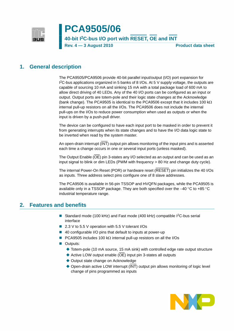
1. General description The PCA9505/PCA9506 provide 40-bit parallel input/output (I/O) port expansion for I 2 C-bus applications organized in 5 banks of 8 I/Os. At 5 V supply voltage, the outputs are capable of sourcing 10 mA and sinking 15 mA with a total package load of 600 mA to allow direct driving of 40 LEDs. Any of the 40 I/O ports can be configured as an input or output. Output ports are totem-pole and their logic state changes at the Acknowledge (bank change). The PCA9505 is identical to the PCA9506 except that it includes 100 kΩ internal pull-up resistors on all the I/Os. The PCA9506 does not include the internal pull-ups on the I/Os to reduce power consumption when used as outputs or when the input is driven by a push-pull driver. The device can be configured to have each input port to be masked in order to prevent it from generating interrupts when its state changes and to have the I/O data logic state to be inverted when read by the system master. An open-drain interrupt (INT ) output pin allows monitoring of the input pins and is asserted each time a change occurs in one or several input ports (unless masked). The Output Enable (OE ) pin 3-states any I/O selected as an output and can be used as an input signal to blink or dim LEDs (PWM with frequency > 80 Hz and change duty cycle). The internal Power-On Reset (POR) or hardware reset (RESET ) pin initializes the 40 I/Os as inputs. Three address select pins configure one of 8 slave addresses. The PCA9506 is available in 56-pin TSSOP and HVQFN packages, while the PCA9505 is available only in a TSSOP package. They are both specified over the −40 °C to +85 °C industrial temperature range. 2. Features and benefits Standard mode (100 kHz) and Fast mode (400 kHz) compatible I 2 C-bus serial interface 2.3 V to 5.5 V operation with 5.5 V tolerant I/Os 40 configurable I/O pins that default to inputs at power-up PCA9505 includes 100 kΩ internal pull-up resistors on all the I/Os Outputs: Totem-pole (10 mA source, 15 mA sink) with controlled edge rate output structure Active LOW output enable (OE ) input pin 3-states all outputs Output state change on Acknowledge Open-drain active LOW interrupt (INT ) output pin allows monitoring of logic level change of pins programmed as inputs PCA9505/06 40-bit I 2 C-bus I/O port with RESET , OE and INT Rev. 4 — 3 August 2010 Product data sheet
Transcript of PCA9505/06 40-bit I2C-bus I/O port with RESET, OE and INT · IO0_7 INPUT/ OUTPUT PORTS BANK 0 write...
1. General description
The PCA9505/PCA9506 provide 40-bit parallel input/output (I/O) port expansion for I2C-bus applications organized in 5 banks of 8 I/Os. At 5 V supply voltage, the outputs are capable of sourcing 10 mA and sinking 15 mA with a total package load of 600 mA to allow direct driving of 40 LEDs. Any of the 40 I/O ports can be configured as an input or output. Output ports are totem-pole and their logic state changes at the Acknowledge (bank change). The PCA9505 is identical to the PCA9506 except that it includes 100 kΩ internal pull-up resistors on all the I/Os. The PCA9506 does not include the internal pull-ups on the I/Os to reduce power consumption when used as outputs or when the input is driven by a push-pull driver.
The device can be configured to have each input port to be masked in order to prevent it from generating interrupts when its state changes and to have the I/O data logic state to be inverted when read by the system master.
An open-drain interrupt (INT) output pin allows monitoring of the input pins and is asserted each time a change occurs in one or several input ports (unless masked).
The Output Enable (OE) pin 3-states any I/O selected as an output and can be used as an input signal to blink or dim LEDs (PWM with frequency > 80 Hz and change duty cycle).
The internal Power-On Reset (POR) or hardware reset (RESET) pin initializes the 40 I/Os as inputs. Three address select pins configure one of 8 slave addresses.
The PCA9506 is available in 56-pin TSSOP and HVQFN packages, while the PCA9505 is available only in a TSSOP package. They are both specified over the −40 °C to +85 °C industrial temperature range.
2. Features and benefits
Standard mode (100 kHz) and Fast mode (400 kHz) compatible I2C-bus serial interface2.3 V to 5.5 V operation with 5.5 V tolerant I/Os40 configurable I/O pins that default to inputs at power-upPCA9505 includes 100 kΩ internal pull-up resistors on all the I/OsOutputs:
Totem-pole (10 mA source, 15 mA sink) with controlled edge rate output structureActive LOW output enable (OE) input pin 3-states all outputsOutput state change on AcknowledgeOpen-drain active LOW interrupt (INT) output pin allows monitoring of logic level change of pins programmed as inputs
PCA9505/0640-bit I2C-bus I/O port with RESET, OE and INTRev. 4 — 3 August 2010 Product data sheet
NXP Semiconductors PCA9505/0640-bit I2C-bus I/O port with RESET, OE and INT
Inputs:Programmable Interrupt Mask Control for input pins that do not require an interrupt when their states changePolarity Inversion register allows inversion of the polarity of the I/O pins when read
Active LOW reset (RESET) input pin resets device to power-up default state3 programmable address pins allowing 8 devices on the same busDesigned for live insertion
Minimize line disturbance (IOFF and power-up 3-state)Signal transient rejection (50 ns noise filter and robust I2C-bus state machine)
Low standby current−40 °C to +85 °C operationESD protection exceeds 2000 V HBM per JESD22-A114, 200 V MM per JESD22-A115, and 1000 V CDM per JESD22-C101Latch-up testing is done to JEDEC Standard JESD78, which exceeds 100 mAOffered in TSSOP56 (PCA9505, PCA9506) and HVQFN56 (PCA9506) packages
3. Applications
ServersRAID systemsIndustrial controlMedical equipmentPLCsCell phonesGaming machinesInstrumentation and test measurement
4. Ordering information
Table 1. Ordering informationType number Topside mark Package
Name Description VersionPCA9505DGG PCA9505DGG TSSOP56 plastic thin shrink small outline package; 56 leads;
body width 6.1 mmSOT364-1
PCA9506DGG PCA9506DGG TSSOP56 plastic thin shrink small outline package; 56 leads; body width 6.1 mm
SOT364-1
PCA9506BS PCA9506BS HVQFN56 plastic thermal enhanced very thin quad flat package; no leads; 56 terminals; body 8 × 8 × 0.85 mm
SOT684-1
PCA9505_9506 All information provided in this document is subject to legal disclaimers. © NXP B.V. 2010. All rights reserved.
Product data sheet Rev. 4 — 3 August 2010 2 of 34
NXP Semiconductors PCA9505/0640-bit I2C-bus I/O port with RESET, OE and INT
5. Block diagram
All I/Os are set to inputs at power-up and RESET.
Fig 1. Block diagram of PCA9505/06
PCA9505/PCA9506
POWER-ONRESET
002aab492
VSS
VDD
RESET
I2C-BUSCONTROL
LOW PASSINPUT
FILTERS
SCL
SDA
A0
A1
INT
OE
8-bit
IO0_0IO0_1IO0_2IO0_3IO0_4IO0_5IO0_6IO0_7
INPUT/OUTPUTPORTS
BANK 0
write pulse 0
read pulse 0
BANK 1
BANK 2
BANK 3
8-bit
IO4_0IO4_1IO4_2IO4_3IO4_4IO4_5IO4_6IO4_7
INPUT/OUTPUTPORTS
BANK 4
write pulse 4
read pulse 4
A2
LP FILTER
INTERRUPTMANAGEMENT
PCA9505_9506 All information provided in this document is subject to legal disclaimers. © NXP B.V. 2010. All rights reserved.
Product data sheet Rev. 4 — 3 August 2010 3 of 34

NXP Semiconductors PCA9505/0640-bit I2C-bus I/O port with RESET, OE and INT
On power-up or RESET, all registers return to default values.
Fig 2. Simplified schematic of IO0_0 to IO4_7
VDD
IOx_y
VSS
configuration port register data (Cx[y])
output port register data (Ox[y])I/O configuration register
D Q
CK Q
data fromshift register
write configurationpulse
output port register
D Q
CK
data fromshift register
write pulse
polarity inversionregister
D Q
CK
data fromshift register
write polaritypulse
ESD protection diode
input port register
D Q
CKread pulse
input portregister data(Ix[y])
INT
polarityregister data(Px[y])
002aab493
INTERRUPTMANAGEMENT
Mx[y]
PCA9505only
100 kΩ
PCA9505_9506 All information provided in this document is subject to legal disclaimers. © NXP B.V. 2010. All rights reserved.
Product data sheet Rev. 4 — 3 August 2010 4 of 34
NXP Semiconductors PCA9505/0640-bit I2C-bus I/O port with RESET, OE and INT
6. Pinning information
6.1 Pinning
Fig 3. Pin configuration for TSSOP56
PCA9505DGGPCA9506DGG
SDA RESET
SCL INT
IO0_0 IO4_7
IO0_1 IO4_6
IO0_2 IO4_5
VSS VSS
IO0_3 IO4_4
IO0_4 IO4_3
IO0_5 IO4_2
IO0_6 IO4_1
VSS VDD
IO0_7 IO4_0
IO1_0 IO3_7
IO1_1 IO3_6
IO1_2 IO3_5
IO1_3 IO3_4
IO1_4 IO3_3
VDD VSS
IO1_5 IO3_2
IO1_6 IO3_1
IO1_7 IO3_0
IO2_0 IO2_7
VSS VSS
IO2_1 IO2_6
IO2_2 IO2_5
IO2_3 IO2_4
A0 OE
A1 A2
002aab491
1
2
3
4
5
6
7
8
9
10
11
12
13
14
15
16
17
18
19
20
21
22
23
24
25
26
27
28
56
55
54
53
52
51
50
49
48
47
46
45
44
43
42
41
40
39
38
37
36
35
34
33
32
31
30
29
PCA9505_9506 All information provided in this document is subject to legal disclaimers. © NXP B.V. 2010. All rights reserved.
Product data sheet Rev. 4 — 3 August 2010 5 of 34
NXP Semiconductors PCA9505/0640-bit I2C-bus I/O port with RESET, OE and INT
6.2 Pin description
Fig 4. Pin configuration for HVQFN56
IO1_5
VDD
002aab975
PCA9506BS
Transparent top view
IO3_0
IO1_6
IO1_7
IO3_1
IO3_2
VSS
IO1_4 IO3_3
IO1_3 IO3_4
IO1_2 IO3_5
IO1_1 IO3_6
IO1_0 IO3_7
IO0_7 IO4_0
VSS VDD
IO0_6 IO4_1
IO0_5 IO4_2
IO0_4 IO4_3
IO2_
0
VS
S
IO2_
1
IO2_
2
IO2_
3
A0
A1
A2
OE
IO2_
4
IO2_
5
IO2_
6
VS
S
IO2_
7
IO0_
3
VS
S
IO0_
2
IO0_
1
IO0_
0
SC
L
SD
A
RE
SE
T
INT
IO4_
7
IO4_
6
IO4_
5
VS
S
IO4_
4
14 29
13 30
12 31
11 32
10 33
9 34
8 35
7 36
6 37
5 38
4 39
3 40
2 41
1 42
15 16 17 18 19 20 21 22 23 24 25 26 27 28
56 55 54 53 52 51 50 49 48 47 46 45 44 43
terminal 1index area
Table 2. Pin descriptionSymbol Pin Type Description
TSSOP56 HVQFN56SDA 1 50 I/O serial data line
SCL 2 51 I serial clock line
IO0_0 to IO0_7 3, 4, 5, 7, 8, 9, 10, 12
52, 53, 54, 56, 1, 2, 3, 5
I/O input/output bank 0
IO1_0 to IO1_7 13, 14, 15, 16, 17, 19, 20, 21
6, 7, 8, 9, 10, 12, 13, 14
I/O input/output bank 1
IO2_0 to IO2_7 22, 24, 25, 26, 31, 32, 33, 35
15, 17, 18, 19, 24, 25, 26, 28
I/O input/output bank 2
IO3_0 to IO3_7 36, 37, 38, 40, 41, 42, 43, 44
29, 30, 31, 33, 34, 35, 36, 37
I/O input/output bank 3
IO4_0 to IO4_7 45, 47, 48, 49, 50, 52, 53, 54
38, 40, 41, 42, 43, 45, 46, 47
I/O input/output bank 4
VSS 6, 11, 23, 34, 39, 51
4, 16, 27, 32, 44, 55[1]
power supply
ground supply voltage
VDD 18, 46 11, 39 power supply
supply voltage
A0 27 20 I address input 0
A1 28 21 I address input 1
A2 29 22 I address input 2
PCA9505_9506 All information provided in this document is subject to legal disclaimers. © NXP B.V. 2010. All rights reserved.
Product data sheet Rev. 4 — 3 August 2010 6 of 34
NXP Semiconductors PCA9505/0640-bit I2C-bus I/O port with RESET, OE and INT
[1] HVQFN56 package die supply ground is connected to both VSS pins and exposed center pad. VSS pins must be connected to supply ground for proper device operation. For enhanced thermal, electrical, and board level performance, the exposed pad needs to be soldered to the board using a corresponding thermal pad on the board and for proper heat conduction through the board, thermal vias need to be incorporated in the printed-circuit board in the thermal pad region.
7. Functional description
Refer to Figure 1 “Block diagram of PCA9505/06” and Figure 2 “Simplified schematic of IO0_0 to IO4_7”.
7.1 Device addressFollowing a START condition, the bus master must send the address of the slave it is accessing and the operation it wants to perform (read or write). The address of the PCA9505/06 is shown in Figure 5. Slave address pins A2, A1, and A0 choose 1 of 8 slave addresses and need to be connected to VDD (1) or VSS (0). To conserve power, no internal pull-up resistors are incorporated on A2, A1, and A0.
The last bit of the first byte defines the operation to be performed. When set to logic 1 a read is selected, while a logic 0 selects a write operation.
7.2 Command registerFollowing the successful acknowledgement of the slave address + R/W bit, the bus master will send a byte to the PCA9505/06, which will be stored in the Command register.
OE 30 23 I active LOW output enable input
INT 55 48 O active LOW interrupt output
RESET 56 49 I active LOW reset input
Table 2. Pin description …continued
Symbol Pin Type DescriptionTSSOP56 HVQFN56
Fig 5. PCA9505/06 address
002aab494
0 1 0 0 A2 A1 A0 R/W
fixed
slave address
programmable
Fig 6. Command register
002aab495
1 0 0 0 0 0 0 0
AI − D5 D4 D3 D2 D1 D0
Auto-Incrementregister number
default at power-upor after RESET
PCA9505_9506 All information provided in this document is subject to legal disclaimers. © NXP B.V. 2010. All rights reserved.
Product data sheet Rev. 4 — 3 August 2010 7 of 34
NXP Semiconductors PCA9505/0640-bit I2C-bus I/O port with RESET, OE and INT
The lowest 6 bits are used as a pointer to determine which register will be accessed. The registers are:
• IP: Input Port registers (5 registers)• OP: Output Port registers (5 registers)• PI: Polarity Inversion registers (5 registers)• IOC: I/O Configuration registers (5 registers)• MSK: Mask interrupt registers (5 registers)
If the Auto-Increment flag is set (AI = 1), the 3 least significant bits are automatically incremented after a read or write. This allows the user to program and/or read the 5 register banks sequentially.
If more than 5 bytes of data are written and AI = 1, previous data in the selected registers will be overwritten. Reserved registers are skipped and not accessed (refer to Table 3).
If the Auto-Increment flag is cleared (AI = 0), the 3 least significant bits are not incremented after data is read or written. During a read operation, the same register bank is read each time. During a write operation, data is written to the same register bank each time.
Only a Command register code with the 5 least significant bits equal to the 25 allowable values as defined in Table 3 are valid. Reserved or undefined command codes must not be accessed for proper device functionality. At power-up, this register defaults to 0x80, with the AI bit set to logic 1, and the lowest 7 bits set to logic 0.
During a write operation, the PCA9505/06 will acknowledge a byte sent to OPx, PIx, and IOCx and MSKx registers, but will not acknowledge a byte sent to the IPx registers since these are read-only registers.
PCA9505_9506 All information provided in this document is subject to legal disclaimers. © NXP B.V. 2010. All rights reserved.
Product data sheet Rev. 4 — 3 August 2010 8 of 34

NXP Semiconductors PCA9505/0640-bit I2C-bus I/O port with RESET, OE and INT
7.3 Register definitions
Table 3. Register summaryRegister # (hex)
D5 D4 D3 D2 D1 D0 Symbol Access Description
Input Port registers00 0 0 0 0 0 0 IP0 read only Input Port register bank 0
01 0 0 0 0 0 1 IP1 read only Input Port register bank 1
02 0 0 0 0 1 0 IP2 read only Input Port register bank 2
03 0 0 0 0 1 1 IP3 read only Input Port register bank 3
04 0 0 0 1 0 0 IP4 read only Input Port register bank 4
05 0 0 0 1 0 1 - - reserved for future use
06 0 0 0 1 1 0 - - reserved for future use
07 0 0 0 1 1 1 - - reserved for future use
Output Port registers08 0 0 1 0 0 0 OP0 read/write Output Port register bank 0
09 0 0 1 0 0 1 OP1 read/write Output Port register bank 1
0A 0 0 1 0 1 0 OP2 read/write Output Port register bank 2
0B 0 0 1 0 1 1 OP3 read/write Output Port register bank 3
0C 0 0 1 1 0 0 OP4 read/write Output Port register bank 4
0D 0 0 1 1 0 1 - - reserved for future use
0E 0 0 1 1 1 0 - - reserved for future use
0F 0 0 1 1 1 1 - - reserved for future use
Polarity Inversion registers10 0 1 0 0 0 0 PI0 read/write Polarity Inversion register bank 0
11 0 1 0 0 0 1 PI1 read/write Polarity Inversion register bank 1
12 0 1 0 0 1 0 PI2 read/write Polarity Inversion register bank 2
13 0 1 0 0 1 1 PI3 read/write Polarity Inversion register bank 3
14 0 1 0 1 0 0 PI4 read/write Polarity Inversion register bank 4
15 0 1 0 1 0 1 - - reserved for future use
16 0 1 0 1 1 0 - - reserved for future use
17 0 1 0 1 1 1 - - reserved for future use
I/O Configuration registers18 0 1 1 0 0 0 IOC0 read/write I/O Configuration register bank 0
19 0 1 1 0 0 1 IOC1 read/write I/O Configuration register bank 1
1A 0 1 1 0 1 0 IOC2 read/write I/O Configuration register bank 2
1B 0 1 1 0 1 1 IOC3 read/write I/O Configuration register bank 3
1C 0 1 1 1 0 0 IOC4 read/write I/O Configuration register bank 4
1D 0 1 1 1 0 1 - - reserved for future use
1E 0 1 1 1 1 0 - - reserved for future use
1F 0 1 1 1 1 1 - - reserved for future use
PCA9505_9506 All information provided in this document is subject to legal disclaimers. © NXP B.V. 2010. All rights reserved.
Product data sheet Rev. 4 — 3 August 2010 9 of 34

NXP Semiconductors PCA9505/0640-bit I2C-bus I/O port with RESET, OE and INT
7.3.1 IP0 to IP4 - Input Port registersThese registers are read-only. They reflect the incoming logic levels of the port pins regardless of whether the pin is defined as an input or an output by the I/O Configuration register. If the corresponding Px[y] bit in the PI registers is set to logic 0, or the inverted incoming logic levels if the corresponding Px[y] bit in the PI register is set to logic 1. Writes to these registers have no effect.
The Polarity Inversion register can invert the logic states of the port pins. The polarity of the corresponding bit is inverted when Px[y] bit in the PI register is set to logic 1. The polarity of the corresponding bit is not inverted when Px[y] bits in the PI register is set to logic 0.
Mask Interrupt registers20 1 0 0 0 0 0 MSK0 read/write Mask Interrupt register bank 0
21 1 0 0 0 0 1 MSK1 read/write Mask Interrupt register bank 1
22 1 0 0 0 1 0 MSK2 read/write Mask Interrupt register bank 2
23 1 0 0 0 1 1 MSK3 read/write Mask Interrupt register bank 3
24 1 0 0 1 0 0 MSK4 read/write Mask Interrupt register bank 4
25 1 0 0 1 0 1 - - reserved for future use
26 1 0 0 1 1 0 - - reserved for future use
27 1 0 0 1 1 1 - - reserved for future use
Table 3. Register summary …continued
Register # (hex)
D5 D4 D3 D2 D1 D0 Symbol Access Description
Table 4. IP0 to IP4 - Input Port registers (address 00h to 04h) bit descriptionLegend: * default value ‘X’ determined by the externally applied logic level.
Address Register Bit Symbol Access Value Description00h IP0 7 to 0 I0[7:0] R XXXX XXXX* Input Port register bank 0
01h IP1 7 to 0 I1[7:0] R XXXX XXXX* Input Port register bank 1
02h IP2 7 to 0 I2[7:0] R XXXX XXXX* Input Port register bank 2
03h IP3 7 to 0 I3[7:0] R XXXX XXXX* Input Port register bank 3
04h IP4 7 to 0 I4[7:0] R XXXX XXXX* Input Port register bank 4
PCA9505_9506 All information provided in this document is subject to legal disclaimers. © NXP B.V. 2010. All rights reserved.
Product data sheet Rev. 4 — 3 August 2010 10 of 34
NXP Semiconductors PCA9505/0640-bit I2C-bus I/O port with RESET, OE and INT
7.3.2 OP0 to OP4 - Output Port registersThese registers reflect the outgoing logic levels of the pins defined as outputs by the I/O Configuration register. Bit values in these registers have no effect on pins defined as inputs. In turn, reads from these registers reflect the values that are in the flip-flops controlling the output selection, not the actual pin values.
Ox[y] = 0: IOx_y = 0 if IOx_y defined as output (Cx[y] in IOC register = 0).Ox[y] = 1: IOx_y = 1 if IOx_y defined as output (Cx[y] in IOC register = 0).
Where ‘x’ refers to the bank number (0 to 4); ‘y’ refers to the bit number (0 to 7).
7.3.3 PI0 to PI4 - Polarity Inversion registersThese registers allow inversion of the polarity of the corresponding Input Port register.
Px[y] = 0: The corresponding Input Port register data polarity is retained.Px[y] = 1: The corresponding Input Port register data polarity is inverted.
Where ‘x’ refers to the bank number (0 to 4); ‘y’ refers to the bit number (0 to 7).
Table 5. OP0 to OP4 - Output Port registers (address 08h to 0Ch) bit descriptionLegend: * default value.
Address Register Bit Symbol Access Value Description08h OP0 7 to 0 O0[7:0] R/W 0000 0000* Output Port register bank 0
09h OP1 7 to 0 O1[7:0] R/W 0000 0000* Output Port register bank 1
0Ah OP2 7 to 0 O2[7:0] R/W 0000 0000* Output Port register bank 2
0Bh OP3 7 to 0 O3[7:0] R/W 0000 0000* Output Port register bank 3
0Ch OP4 7 to 0 O4[7:0] R/W 0000 0000* Output Port register bank 4
Table 6. PI0 to PI4 - Polarity Inversion registers (address 10h to 14h) bit descriptionLegend: * default value.
Address Register Bit Symbol Access Value Description10h PI0 7 to 0 P0[7:0] R/W 0000 0000* Polarity Inversion register bank 0
11h PI1 7 to 0 P1[7:0] R/W 0000 0000* Polarity Inversion register bank 1
12h PI2 7 to 0 P2[7:0] R/W 0000 0000* Polarity Inversion register bank 2
13h PI3 7 to 0 P3[7:0] R/W 0000 0000* Polarity Inversion register bank 3
14h PI4 7 to 0 P4[7:0] R/W 0000 0000* Polarity Inversion register bank 4
PCA9505_9506 All information provided in this document is subject to legal disclaimers. © NXP B.V. 2010. All rights reserved.
Product data sheet Rev. 4 — 3 August 2010 11 of 34

NXP Semiconductors PCA9505/0640-bit I2C-bus I/O port with RESET, OE and INT
7.3.4 IOC0 to IOC4 - I/O Configuration registersThese registers configure the direction of the I/O pins.
Cx[y] = 0: The corresponding port pin is an output.Cx[y] = 1: The corresponding port pin is an input.
Where ‘x’ refers to the bank number (0 to 4); ‘y’ refers to the bit number (0 to 7).
7.3.5 MSK0 to MSK4 - Mask interrupt registersThese registers mask the interrupt due to a change in the I/O pins configured as inputs. ‘x’ refers to the bank number (0 to 4); ‘y’ refers to the bit number (0 to 7).
Mx[y] = 0: A level change at the I/O will generate an interrupt if IOx_y defined as input (Cx[y] in IOC register = 1).Mx[y] = 1: A level change in the input port will not generate an interrupt if IOx_y defined as input (Cx[y] in IOC register = 1).
7.4 Power-on resetWhen power is applied to VDD, an internal Power-On Reset (POR) holds the PCA9505/06 in a reset condition until VDD has reached VPOR. At that point, the reset condition is released and the PCA9505/06 registers and I2C-bus state machine will initialize to their default states. Thereafter, VDD must be lowered below 0.2 V to reset the device.
7.5 RESET inputA reset can be accomplished by holding the RESET pin LOW for a minimum of tw(rst). The PCA9505/06 registers and I2C-bus state machine will be held in their default states until the RESET input is once again HIGH.
Table 7. IOC0 to IOC4 - I/O Configuration registers (address 18h to 1Ch) bit descriptionLegend: * default value.
Address Register Bit Symbol Access Value Description18h IOC0 7 to 0 C0[7:0] R/W 1111 1111* I/O Configuration register bank 0
19h IOC1 7 to 0 C1[7:0] R/W 1111 1111* I/O Configuration register bank 1
1Ah IOC2 7 to 0 C2[7:0] R/W 1111 1111* I/O Configuration register bank 2
1Bh IOC3 7 to 0 C3[7:0] R/W 1111 1111* I/O Configuration register bank 3
1Ch IOC4 7 to 0 C4[7:0] R/W 1111 1111* I/O Configuration register bank 4
Table 8. MSK0 to MSK4 - Mask interrupt registers (address 20h to 24h) bit descriptionLegend: * default value.
Address Register Bit Symbol Access Value Description20h MSK0 7 to 0 M0[7:0] R/W 1111 1111* Mask Interrupt register bank 0
21h MSK1 7 to 0 M1[7:0] R/W 1111 1111* Mask Interrupt register bank 1
22h MSK2 7 to 0 M2[7:0] R/W 1111 1111* Mask Interrupt register bank 2
23h MSK3 7 to 0 M3[7:0] R/W 1111 1111* Mask Interrupt register bank 3
24h MSK4 7 to 0 M4[7:0] R/W 1111 1111* Mask Interrupt register bank 4
PCA9505_9506 All information provided in this document is subject to legal disclaimers. © NXP B.V. 2010. All rights reserved.
Product data sheet Rev. 4 — 3 August 2010 12 of 34

NXP Semiconductors PCA9505/0640-bit I2C-bus I/O port with RESET, OE and INT
7.6 Interrupt output (INT)The open-drain active LOW interrupt is activated when one of the port pins changes state and the port pin is configured as an input and the interrupt on it is not masked. The interrupt is deactivated when the port pin input returns to its previous state or the Input Port register is read.
Remark: Changing an I/O from an output to an input may cause a false interrupt to occur if the state of the pin does not match the contents of the Input Port register.
Only a read of the Input Port register that contains the bit(s) image of the input(s) that generated the interrupt clears the interrupt condition.
If more than one input register changed state before a read of the Input Port register is initiated, the interrupt is cleared when all the input registers containing all the inputs that changed are read.
Example: If IO0_5, IO2_3, and IO3_7 change state at the same time, the interrupt is cleared only when INREG0, INREG2, and INREG3 are read.
7.7 Output enable input (OE)The active LOW output enable pin allows to enable or disable all the I/Os at the same time. When a LOW level is applied to the OE pin, all the I/Os configured as outputs are enabled and the logic value programmed in their respective OP registers is applied to the pins. When a HIGH level is applied to the OE pin, all the I/Os configured as outputs are 3-stated.
For applications requiring LED blinking with brightness control, this pin can be used to control the brightness by applying a high frequency PWM signal on the OE pin. LEDs can be blinked using the Output Port registers and can be dimmed using the PWM signal on the OE pin thus controlling the brightness by adjusting the duty cycle.
7.8 Live insertionThe PCA9505/06 are fully specified for live insertion applications using IOFF, power-up 3-states, robust state machine, and 50 ns noise filter. The IOFF circuitry disables the outputs, preventing damaging current backflow through the device when it is powered down. The power-up 3-state’s circuitry places the outputs in the high-impedance state during power-up and power-down, which prevents driver conflict and bus contention.
The robust state machine does not respond until it sees a valid START condition and the 50 ns noise filter will filter out any insertion glitches. The PCA9505/06 will not cause corruption of active data on the bus, nor will the device be damaged or cause damage to devices already on the bus when similar featured devices are being used.
7.9 StandbyThe PCA9505/06 goes into standby when the I2C-bus is idle. Standby supply current is lower than 1 μA (typical).
PCA9505_9506 All information provided in this document is subject to legal disclaimers. © NXP B.V. 2010. All rights reserved.
Product data sheet Rev. 4 — 3 August 2010 13 of 34

NXP Semiconductors PCA9505/0640-bit I2C-bus I/O port with RESET, OE and INT
8. Characteristics of the I2C-bus
The I2C-bus is for 2-way, 2-line communication between different ICs or modules. The two lines are a serial data line (SDA) and a serial clock line (SCL). Both lines must be connected to a positive supply via a pull-up resistor when connected to the output stages of a device. Data transfer may be initiated only when the bus is not busy.
8.1 Bit transferOne data bit is transferred during each clock pulse. The data on the SDA line must remain stable during the HIGH period of the clock pulse as changes in the data line at this time will be interpreted as control signals (see Figure 7).
8.1.1 START and STOP conditionsBoth data and clock lines remain HIGH when the bus is not busy. A HIGH-to-LOW transition of the data line while the clock is HIGH is defined as the START condition (S). A LOW-to-HIGH transition of the data line while the clock is HIGH is defined as the STOP condition (P) (see Figure 8).
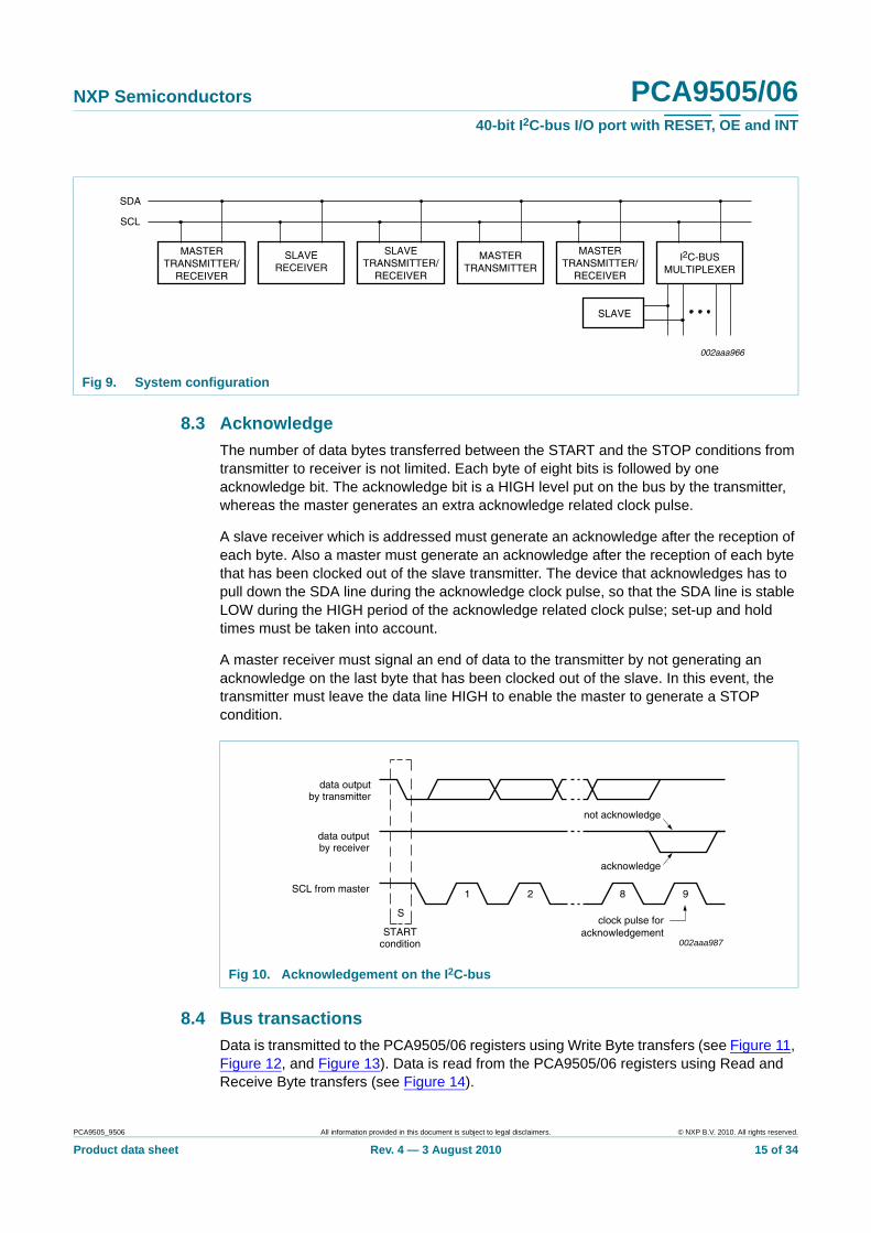
8.2 System configurationA device generating a message is a ‘transmitter’; a device receiving is the ‘receiver’. The device that controls the message is the ‘master' and the devices which are controlled by the master are the ‘slaves' (see Figure 9).
Fig 7. Bit transfer
mba607
data linestable;
data valid
changeof dataallowed
SDA
SCL
Fig 8. Definition of START and STOP conditions
mba608
SDA
SCLP
STOP condition
S
START condition
PCA9505_9506 All information provided in this document is subject to legal disclaimers. © NXP B.V. 2010. All rights reserved.
Product data sheet Rev. 4 — 3 August 2010 14 of 34
NXP Semiconductors PCA9505/0640-bit I2C-bus I/O port with RESET, OE and INT
8.3 AcknowledgeThe number of data bytes transferred between the START and the STOP conditions from transmitter to receiver is not limited. Each byte of eight bits is followed by one acknowledge bit. The acknowledge bit is a HIGH level put on the bus by the transmitter, whereas the master generates an extra acknowledge related clock pulse.
A slave receiver which is addressed must generate an acknowledge after the reception of each byte. Also a master must generate an acknowledge after the reception of each byte that has been clocked out of the slave transmitter. The device that acknowledges has to pull down the SDA line during the acknowledge clock pulse, so that the SDA line is stable LOW during the HIGH period of the acknowledge related clock pulse; set-up and hold times must be taken into account.
A master receiver must signal an end of data to the transmitter by not generating an acknowledge on the last byte that has been clocked out of the slave. In this event, the transmitter must leave the data line HIGH to enable the master to generate a STOP condition.
8.4 Bus transactionsData is transmitted to the PCA9505/06 registers using Write Byte transfers (see Figure 11, Figure 12, and Figure 13). Data is read from the PCA9505/06 registers using Read and Receive Byte transfers (see Figure 14).
Fig 9. System configuration
002aaa966
MASTERTRANSMITTER/
RECEIVER
SLAVERECEIVER
SLAVETRANSMITTER/
RECEIVER
MASTERTRANSMITTER
MASTERTRANSMITTER/
RECEIVER
SDA
SCL
I2C-BUSMULTIPLEXER
SLAVE
Fig 10. Acknowledgement on the I2C-bus
002aaa987
S
STARTcondition
9821
clock pulse foracknowledgement
not acknowledge
acknowledge
data outputby transmitter
data outputby receiver
SCL from master
PCA9505_9506 All information provided in this document is subject to legal disclaimers. © NXP B.V. 2010. All rights reserved.
Product data sheet Rev. 4 — 3 August 2010 15 of 34
xxxxxxxxxxxxxxxxxxxxx xxxxxxxxxxxxxxxxxxxxxxxxxx xxxxxxx x x x xxxxxxxxxxxxxxxxxxxxxxxxxxxxxx xxxxxxxxxxxxxxxxxxx xx xx xxxxx xxxxxxxxxxxxxxxxxxxxxxxxxxx xxxxxxxxxxxxxxxxxxx xxxxxx xxxxxxxxxxxxxxxxxxxxxxxxxxxxxxxxxxx xxxxxxxxxxxx x x xxxxxxxxxxxxxxxxxxxxx xxxxxxxxxxxxxxxxxxxxxxxxxxxxxx xxxxx xxxxxxxxxxxxxxxxxxxxxxxxxxxxxxxxxxxxxxxxxxxxxxxxxx xxxxxxxx xxxxxxxxxxxxxxxxxxxxxxxxx xxxxxxxxxxxxxxxxxxxx xxx
PCA
9505_9506
Product data sh
NXP Sem
iconductorsPC
A9505/06
40-bit I 2C-bus I/O
port with R
ESET, OE and IN
T
002aab496
slave address command register
NK 3 P
STOPcondition
A
wledgem slave
DATA BANK 4 A
acknowledgefrom slave
ata validbank 2
data validbank 3
data validbank 4
All information provided in this docum
ent is subject to legal disclaimers.
© N
XP B.V. 2010. All rights reserved.
eetR
ev. 4 — 3 A
ugust 2010 16 of 34
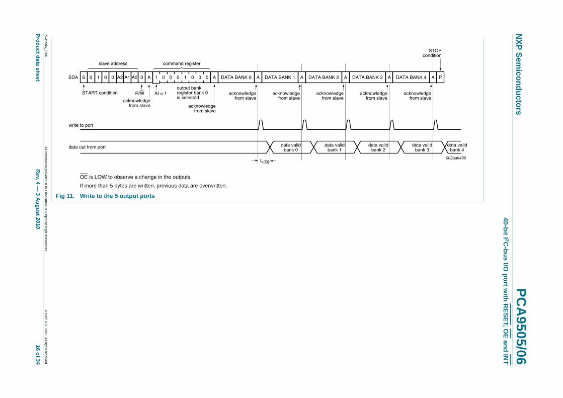
OE is LOW to observe a change in the outputs.If more than 5 bytes are written, previous data are overwritten.
Fig 11. Write to the 5 output ports
0 1 0 0 A2 A1 A0 0
R/W
S
START condition
SDA A
acknowledgefrom slave
1 0 0 0 1 0 0 0
AI = 1
A
acknowledgefrom slave
DATA BANK 0 A
acknowledgefrom slave
DATA BANK 1 A
acknowledgefrom slave
DATA BANK 2 A
acknowledgefrom slave
DATA BA
acknofro
output bank register bank 0is selected
write to port
data out from port
tv(Q)
data validbank 0
data validbank 1
d

xxxxxxxxxxxxxxxxxxxxx xxxxxxxxxxxxxxxxxxxxxxxxxx xxxxxxx x x x xxxxxxxxxxxxxxxxxxxxxxxxxxxxxx xxxxxxxxxxxxxxxxxxx xx xx xxxxx xxxxxxxxxxxxxxxxxxxxxxxxxxx xxxxxxxxxxxxxxxxxxx xxxxxx xxxxxxxxxxxxxxxxxxxxxxxxxxxxxxxxxxx xxxxxxxxxxxx x x xxxxxxxxxxxxxxxxxxxxx xxxxxxxxxxxxxxxxxxxxxxxxxxxxxx xxxxx xxxxxxxxxxxxxxxxxxxxxxxxxxxxxxxxxxxxxxxxxxxxxxxxxx xxxxxxxx xxxxxxxxxxxxxxxxxxxxxxxxx xxxxxxxxxxxxxxxxxxxx xxx
PCA
9505_9506
Product data sh
NXP Sem
iconductorsPC
A9505/06
40-bit I 2C-bus I/O
port with R
ESET, OE and IN
T
esponding output port becomes effective at
2aab497
0 1 0 0 A2 A1 A0 0
slave address
SSDA A AI 0 0 0 1 D2 D1 D0 A DATA BANK X A P
n
A
ata Xvalid
mmed.ssed Configuration register, the sixth Polarity ver to the first addressed Mask Interrupt
002aab498
TA BANK 3 P
STOPcondition
A
acknowledgefrom slave
DATA BANK 4 A
acknowledgefrom slave
wledgelave
All information provided in this docum
ent is subject to legal disclaimers.
© N
XP B.V. 2010. All rights reserved.
eetR
ev. 4 — 3 A
ugust 2010 17 of 34
OE is LOW to observe a change in the outputs.Two, three, or four adjacent banks can be programmed by using the Auto-Increment feature (AI = 1) and change at the correach acknowledge.
Fig 12. Write to a specific output port
00
R/WSTART condition
acknowledgefrom slave
acknowledgefrom slave
acknowledgefrom slave
STOPconditio
write to port
data out from port
tv(Q)
d
The programming becomes effective at the acknowledge.Less than 5 bytes can be programmed by using this scheme. D5, D4, D3, D2, D1, D0 refers to the first register to be prograIf more than 5 bytes are written, previous data are overwritten (the sixth Configuration register will roll over to the first addreInversion register will roll over to the first addressed Polarity Inversion register and the sixth Mask Interrupt register will roll oregister).
Fig 13. Write to the I/O Configuration, Polarity Inversion or Mask Interrupt registers
0 1 0 0 A2 A1 A0 0
slave address
R/W
S
START condition
SDA A
acknowledgefrom slave
1 0 D5 D4 D3 D2 D1 D0
command register
AI = 1
A
acknowledgefrom slave
DATA BANK 0 A DATA BANK 1 A DATA BANK 2 A DA
acknowledgefrom slave
D[5:0] = 01 0000 for Polarity Inversion register programming bank 0
D[5:0] = 01 1000 for Configuration register programming bank 0
acknowledgefrom slave
acknofrom s
D[5:0] = 10 0000 for Mask Interrupt register programming bank 0
xxxxxxxxxxxxxxxxxxxxx xxxxxxxxxxxxxxxxxxxxxxxxxx xxxxxxx x x x xxxxxxxxxxxxxxxxxxxxxxxxxxxxxx xxxxxxxxxxxxxxxxxxx xx xx xxxxx xxxxxxxxxxxxxxxxxxxxxxxxxxx xxxxxxxxxxxxxxxxxxx xxxxxx xxxxxxxxxxxxxxxxxxxxxxxxxxxxxxxxxxx xxxxxxxxxxxx x x xxxxxxxxxxxxxxxxxxxxx xxxxxxxxxxxxxxxxxxxxxxxxxxxxxx xxxxx xxxxxxxxxxxxxxxxxxxxxxxxxxxxxxxxxxxxxxxxxxxxxxxxxx xxxxxxxx xxxxxxxxxxxxxxxxxxxxxxxxx xxxxxxxxxxxxxxxxxxxx xxx
PCA
9505_9506
Product data sh
NXP Sem
iconductorsPC
A9505/06
40-bit I 2C-bus I/O
port with R
ESET, OE and IN
T
f the category (see category definition in
2_4 and IO4_7 change at the same time and d).
002aab499
0 1 0 0 0
slave address
SSDA A 1 0 D5 D4 D3 D2 D1 D0
command register
A
STOPcondition
Sr
repeated START condition
0 1 0 0 1
slave address
A (cont.)
At this moment master-transmitter becomes master-receiver, and slave-receiver becomes slave-transmitter.
cknowledge from master
A2 A1 A0 A2 A1 A0
All information provided in this docum
ent is subject to legal disclaimers.
© N
XP B.V. 2010. All rights reserved.
eetR
ev. 4 — 3 A
ugust 2010 18 of 34
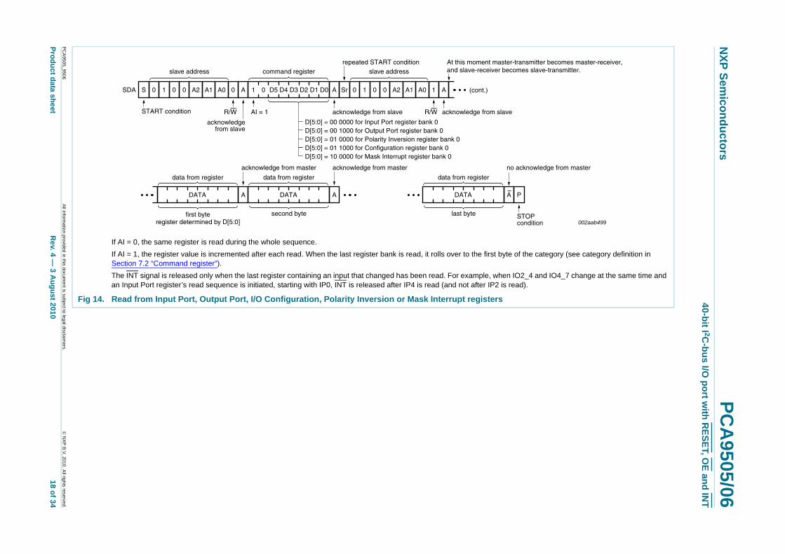
If AI = 0, the same register is read during the whole sequence.If AI = 1, the register value is incremented after each read. When the last register bank is read, it rolls over to the first byte oSection 7.2 “Command register”).The INT signal is released only when the last register containing an input that changed has been read. For example, when IOan Input Port register’s read sequence is initiated, starting with IP0, INT is released after IP4 is read (and not after IP2 is rea
Fig 14. Read from Input Port, Output Port, I/O Configuration, Polarity Inversion or Mask Interrupt registers
R/WSTART condition
acknowledgefrom slave
AI = 1 acknowledge from slave
A PA
acknowledge from master
D[5:0] = 00 1000 for Output Port register bank 0D[5:0] = 01 0000 for Polarity Inversion register bank 0
R/W acknowledge from slave
D[5:0] = 01 1000 for Configuration register bank 0
DATA
data from register
first byteregister determined by D[5:0]
A
acknowledge from master
DATA
data from register
second byte
DATA
data from register
last byte
no a
D[5:0] = 00 0000 for Input Port register bank 0
D[5:0] = 10 0000 for Mask Interrupt register bank 0
NXP Semiconductors PCA9505/0640-bit I2C-bus I/O port with RESET, OE and INT
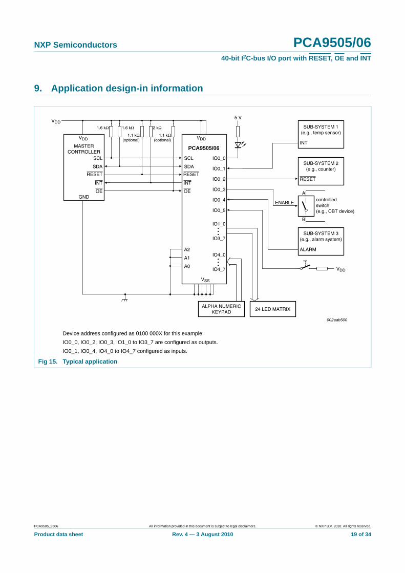
9. Application design-in information
Device address configured as 0100 000X for this example.IO0_0, IO0_2, IO0_3, IO1_0 to IO3_7 are configured as outputs.IO0_1, IO0_4, IO4_0 to IO4_7 configured as inputs.
Fig 15. Typical application
PCA9505/06
IO0_0
IO0_1
SCL
SDA
VDD
MASTERCONTROLLER
SCL
SDA
1.6 kΩ
INT
1.6 kΩ
IO0_2
VDD
A2
A1
A0
5 V
VDD
RESET
OEGND
1.1 kΩ(optional)
OE
INT
RESET
2 kΩ
1.1 kΩ(optional)
SUB-SYSTEM 1(e.g., temp sensor)
IO0_3
INT
SUB-SYSTEM 2(e.g., counter)
RESET
controlledswitch(e.g., CBT device)
VDD
A
B
ENABLE
SUB-SYSTEM 3(e.g., alarm system)
ALARM
IO0_4
IO0_5
IO1_0
IO3_7
IO4_0
IO4_7
24 LED MATRIXALPHA NUMERIC
KEYPAD
VSS
002aab500
PCA9505_9506 All information provided in this document is subject to legal disclaimers. © NXP B.V. 2010. All rights reserved.
Product data sheet Rev. 4 — 3 August 2010 19 of 34

NXP Semiconductors PCA9505/0640-bit I2C-bus I/O port with RESET, OE and INT
10. Limiting values
11. Static characteristics
Table 9. Limiting valuesIn accordance with the Absolute Maximum Rating System (IEC 60134).
Symbol Parameter Conditions Min Max UnitVDD supply voltage −0.5 +6 V
VI input voltage VSS − 0.5 5.5 V
II input current - ±20 mA
VI/O(n) input/output voltage on any other pin VSS − 0.5 5.5 V
VI/O(IO0n) input/output voltage on pin IO0_n VSS − 0.5 5.5 V
IO(I/On) output current on an I/O pin −20 +50 mA
IDD supply current - 500 mA
ISS ground supply current - 1100 mA
Ptot total power dissipation - 500 mW
Tstg storage temperature −65 +150 °C
Tamb ambient temperature operating −40 +85 °C
Tj junction temperature operating - 125 °C
storage - 150 °C
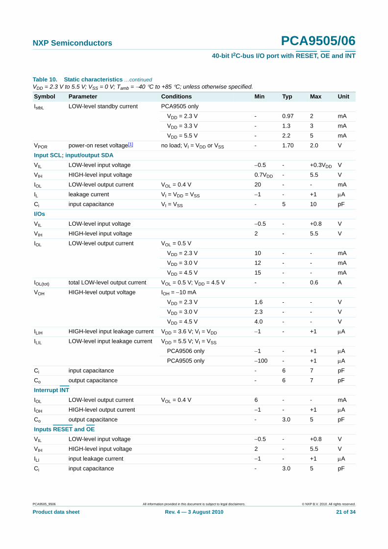
Table 10. Static characteristicsVDD = 2.3 V to 5.5 V; VSS = 0 V; Tamb = −40 °C to +85 °C; unless otherwise specified.
Symbol Parameter Conditions Min Typ Max UnitSupplyVDD supply voltage 2.3 - 5.5 V
IDD supply current PCA9506 only; operating mode; no load; fSCL = 400 kHz
VDD = 2.3 V - 56 95 μA
VDD = 3.3 V - 98 150 μA
VDD = 5.5 V - 225 300 μA
PCA9505 only; operating mode; no load; fSCL = 400 kHz
VDD = 2.3 V - 1 1.5 mA
VDD = 3.3 V - 1.5 2 mA
VDD = 5.5 V - 2.7 3.5 mA
IstbH HIGH-level standby current no load; fSCL = 0 kHz; I/O = inputs; VI = VDD
VDD = 2.3 V - 0.15 11 μA
VDD = 3.3 V - 0.25 12 μA
VDD = 5.5 V - 0.75 15.5 μA
PCA9505_9506 All information provided in this document is subject to legal disclaimers. © NXP B.V. 2010. All rights reserved.
Product data sheet Rev. 4 — 3 August 2010 20 of 34
NXP Semiconductors PCA9505/0640-bit I2C-bus I/O port with RESET, OE and INT
IstbL LOW-level standby current PCA9505 only
VDD = 2.3 V - 0.97 2 mA
VDD = 3.3 V - 1.3 3 mA
VDD = 5.5 V - 2.2 5 mA
VPOR power-on reset voltage[1] no load; VI = VDD or VSS - 1.70 2.0 V
Input SCL; input/output SDAVIL LOW-level input voltage −0.5 - +0.3VDD V
VIH HIGH-level input voltage 0.7VDD - 5.5 V
IOL LOW-level output current VOL = 0.4 V 20 - - mA
IL leakage current VI = VDD = VSS −1 - +1 μA
Ci input capacitance VI = VSS - 5 10 pF
I/OsVIL LOW-level input voltage −0.5 - +0.8 V
VIH HIGH-level input voltage 2 - 5.5 V
IOL LOW-level output current VOL = 0.5 V
VDD = 2.3 V 10 - - mA
VDD = 3.0 V 12 - - mA
VDD = 4.5 V 15 - - mA
IOL(tot) total LOW-level output current VOL = 0.5 V; VDD = 4.5 V - - 0.6 A
VOH HIGH-level output voltage IOH = −10 mA
VDD = 2.3 V 1.6 - - V
VDD = 3.0 V 2.3 - - V
VDD = 4.5 V 4.0 - - V
ILIH HIGH-level input leakage current VDD = 3.6 V; VI = VDD −1 - +1 μA
ILIL LOW-level input leakage current VDD = 5.5 V; VI = VSS
PCA9506 only −1 - +1 μA
PCA9505 only −100 - +1 μA
Ci input capacitance - 6 7 pF
Co output capacitance - 6 7 pF
Interrupt INTIOL LOW-level output current VOL = 0.4 V 6 - - mA
IOH HIGH-level output current −1 - +1 μA
Co output capacitance - 3.0 5 pF
Inputs RESET and OEVIL LOW-level input voltage −0.5 - +0.8 V
VIH HIGH-level input voltage 2 - 5.5 V
ILI input leakage current −1 - +1 μA
Ci input capacitance - 3.0 5 pF
Table 10. Static characteristics …continuedVDD = 2.3 V to 5.5 V; VSS = 0 V; Tamb = −40 °C to +85 °C; unless otherwise specified.
Symbol Parameter Conditions Min Typ Max Unit
PCA9505_9506 All information provided in this document is subject to legal disclaimers. © NXP B.V. 2010. All rights reserved.
Product data sheet Rev. 4 — 3 August 2010 21 of 34

NXP Semiconductors PCA9505/0640-bit I2C-bus I/O port with RESET, OE and INT
[1] VDD must be lowered to 0.2 V in order to reset part.
12. Dynamic characteristics
Inputs A0, A1, A2VIL LOW-level input voltage −0.5 - +0.3VDD V
VIH HIGH-level input voltage 0.7VDD - 5.5 V
ILI input leakage current −1 - +1 μA
Ci input capacitance - 3.5 5 pF
Table 10. Static characteristics …continuedVDD = 2.3 V to 5.5 V; VSS = 0 V; Tamb = −40 °C to +85 °C; unless otherwise specified.
Symbol Parameter Conditions Min Typ Max Unit
Table 11. Dynamic characteristicsSymbol Parameter Conditions Standard mode
I2C-busFast mode I2C-bus Unit
Min Max Min MaxfSCL SCL clock frequency [1] 0 100 0 400 kHz
tBUF bus free time between a STOP and START condition
4.7 - 1.3 - μs
tHD;STA hold time (repeated) START condition
4.0 - 0.6 - μs
tSU;STA set-up time for a repeated START condition
4.7 - 0.6 - μs
tSU;STO set-up time for STOP condition 4.0 - 0.6 - μs
tHD;DAT data hold time 0 - 0 - ns
tVD;ACK data valid acknowledge time[2] 0.1 3.45 0.1 0.9 μs
tVD;DAT data valid time[3] 0.1 3.45 0.1 0.9 μs
tSU;DAT data set-up time 250 - 100 - ns
tLOW LOW period of the SCL clock 4.7 - 1.3 - μs
tHIGH HIGH period of the SCL clock 4.0 - 0.6 - μs
tf fall time of both SDA and SCL signals
[4][5] - 300 20 + 0.1Cb[6] 300 ns
tr rise time of both SDA and SCL signals
[4][5] - 1000 20 + 0.1Cb[6] 300 ns
tSP pulse width of spikes that must be suppressed by the input filter
[7] - 50 - 50 ns
Port timingten enable time output - 80 - 80 ns
tdis disable time output - 40 - 40 ns
tv(Q) data output valid time - 250 - 250 ns
tsu(D) data input set-up time 100 - 100 - ns
th(D) data input hold time 0.5 - 0.5 - μs
Interrupt timingtv(INT_N) valid time on pin INT_N - 4 - 4 μs
trst(INT_N) reset time on pin INT_N - 4 - 4 μs
PCA9505_9506 All information provided in this document is subject to legal disclaimers. © NXP B.V. 2010. All rights reserved.
Product data sheet Rev. 4 — 3 August 2010 22 of 34

NXP Semiconductors PCA9505/0640-bit I2C-bus I/O port with RESET, OE and INT
[1] Minimum SCL clock frequency is limited by the bus time-out feature, which resets the serial bus interface if either SDA or SCL is held LOW for a minimum of 25 ms. Disable bus time-out feature for DC operation.
[2] tVD;ACK = time for Acknowledgement signal from SCL LOW to SDA (out) LOW.
[3] tVD;DAT = minimum time for SDA data out to be valid following SCL LOW.
[4] A master device must internally provide a hold time of at least 300 ns for the SDA signal (refer to the VIL of the SCL signal) in order to bridge the undefined region SCL’s falling edge.
[5] The maximum tf for the SDA and SCL bus lines is specified at 300 ns. The maximum fall time for the SDA output stage tf is specified at 250 ns. This allows series protection resistors to be connected between the SDA and the SCL pins and the SDA/SCL bus lines without exceeding the maximum specified tf.
[6] Cb = total capacitance of one bus line in pF.
[7] Input filters on the SDA and SCL inputs suppress noise spikes less than 50 ns.
Resettw(rst) reset pulse width 4 - 4 - ns
trec(rst) reset recovery time 0 - 0 - ns
trst reset time 100 - 100 - ns
Table 11. Dynamic characteristics …continued
Symbol Parameter Conditions Standard mode I2C-bus
Fast mode I2C-bus Unit
Min Max Min Max
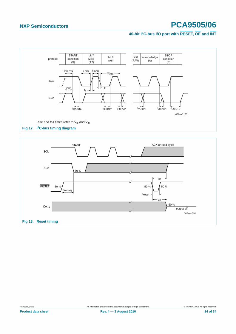
Fig 16. Definition of timing on the I2C-bus
tSPtBUF
tHD;STA
PP S
tLOW
tr
tHD;DAT
tf
tHIGH tSU;DAT
tSU;STA
Sr
tHD;STA
tSU;STO
SDA
SCL
002aaa986
PCA9505_9506 All information provided in this document is subject to legal disclaimers. © NXP B.V. 2010. All rights reserved.
Product data sheet Rev. 4 — 3 August 2010 23 of 34
NXP Semiconductors PCA9505/0640-bit I2C-bus I/O port with RESET, OE and INT
Rise and fall times refer to VIL and VIH.
Fig 17. I2C-bus timing diagram
SCL
SDA
tHD;STA tSU;DAT tHD;DAT
tftBUF
tSU;STA tLOW tHIGH
tVD;ACK
002aab175
tSU;STO
protocolSTART
condition(S)
bit 7MSB(A7)
bit 6(A6)
bit 0(R/W)
acknowledge(A)
STOPcondition
(P)
1/fSCL
tr
tVD;DAT
Fig 18. Reset timing
SDA
SCL
002aac018
trst
50 %
30 %
50 % 50 %
50 %
trec(rst)
tw(rst)
RESET
IOx_youtput off
START
trst
ACK or read cycle
PCA9505_9506 All information provided in this document is subject to legal disclaimers. © NXP B.V. 2010. All rights reserved.
Product data sheet Rev. 4 — 3 August 2010 24 of 34

NXP Semiconductors PCA9505/0640-bit I2C-bus I/O port with RESET, OE and INT
13. Test information
RL = load resistanceCL = load capacitance includes jig and probe capacitanceRT = termination resistance should be equal to the output impedance Zo of the pulse generators.
Fig 19. Test circuitry for switching times
PULSEGENERATOR
VO
CL50 pF
RL500 Ω
002aac019
RT
VI
VDD
DUT
2VDDopenVSS
500 Ω
PCA9505_9506 All information provided in this document is subject to legal disclaimers. © NXP B.V. 2010. All rights reserved.
Product data sheet Rev. 4 — 3 August 2010 25 of 34
NXP Semiconductors PCA9505/0640-bit I2C-bus I/O port with RESET, OE and INT
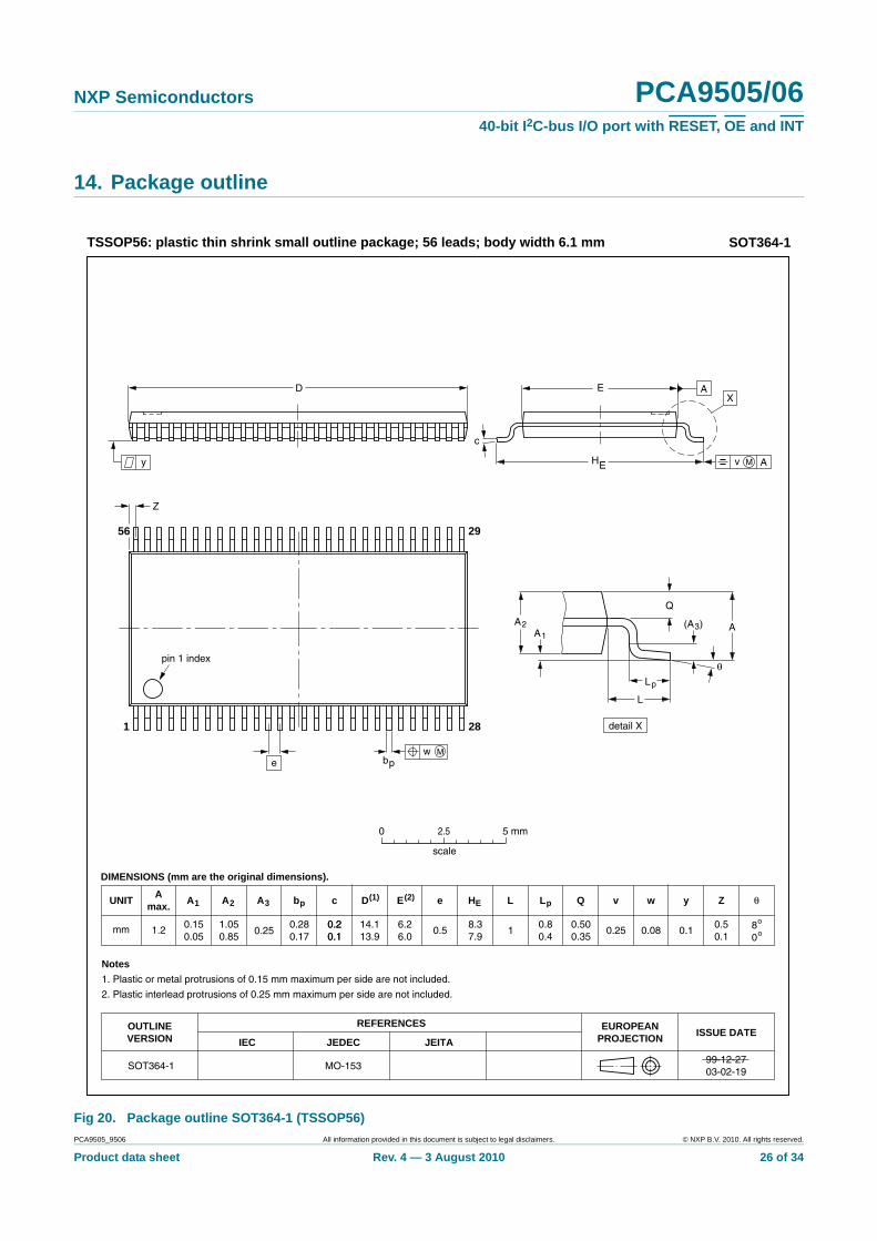
14. Package outline
Fig 20. Package outline SOT364-1 (TSSOP56)
UNIT A1 A2 A3 bp c D(1) E(2) e HE L Lp Q Zywv θ
REFERENCESOUTLINEVERSION
EUROPEANPROJECTION ISSUE DATE
IEC JEDEC JEITA
mm 0.150.05
0.20.1
80
o
o0.1
DIMENSIONS (mm are the original dimensions).
Notes
1. Plastic or metal protrusions of 0.15 mm maximum per side are not included.
2. Plastic interlead protrusions of 0.25 mm maximum per side are not included.
SOT364-199-12-2703-02-19
w M
θ
AA1
A2
D
Lp
Q
detail X
E
Z
e
c
L
X
(A )3
0.25
1 28
56 29
y
pin 1 index
b
H
1.050.85
0.280.17
0.20.1
14.113.9
6.26.0
0.5 18.37.9
0.500.35
0.50.1
0.080.250.80.4
p
E v M A
A
TSSOP56: plastic thin shrink small outline package; 56 leads; body width 6.1 mm SOT364-1
Amax.
1.2
0 2.5 5 mm
scale
MO-153
PCA9505_9506 All information provided in this document is subject to legal disclaimers. © NXP B.V. 2010. All rights reserved.
Product data sheet Rev. 4 — 3 August 2010 26 of 34
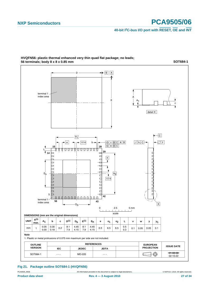
NXP Semiconductors PCA9505/0640-bit I2C-bus I/O port with RESET, OE and INT
Fig 21. Package outline SOT684-1 (HVQFN56)
0.51
A1 EhbUNIT ye
0.2
c
REFERENCESOUTLINEVERSION
EUROPEANPROJECTION ISSUE DATE
IEC JEDEC JEITA
mm
Dh
4.454.15
y1
4.454.15
e1
6.5
e2
6.50.300.18
0.050.00
8.17.9
8.17.9
0.05 0.1
DIMENSIONS (mm are the original dimensions)
SOT684-1 MO-220 - - -- - -
0.50.3
L
0.1
v
0.05
w
0 2.5 5 mm
scale
SOT684-1HVQFN56: plastic thermal enhanced very thin quad flat package; no leads;56 terminals; body 8 x 8 x 0.85 mm
A(1)
max.
AA1
c
detail X
yy1 Ce
L
Eh
Dh
e
e1
b
15 28
56 43
42
2914
1
X
D
E
C
B A
e2
01-08-0802-10-22
terminal 1index area
terminal 1index area
1/2 e
1/2 e
ACC
Bv M
w M
E(1)
Note
1. Plastic or metal protrusions of 0.075 mm maximum per side are not included.
D(1)
PCA9505_9506 All information provided in this document is subject to legal disclaimers. © NXP B.V. 2010. All rights reserved.
Product data sheet Rev. 4 — 3 August 2010 27 of 34

NXP Semiconductors PCA9505/0640-bit I2C-bus I/O port with RESET, OE and INT
15. Handling information
All input and output pins are protected against ElectroStatic Discharge (ESD) under normal handling. When handling ensure that the appropriate precautions are taken as described in JESD625-A or equivalent standards.
16. Soldering of SMD packages
This text provides a very brief insight into a complex technology. A more in-depth account of soldering ICs can be found in Application Note AN10365 “Surface mount reflow soldering description”.
16.1 Introduction to solderingSoldering is one of the most common methods through which packages are attached to Printed Circuit Boards (PCBs), to form electrical circuits. The soldered joint provides both the mechanical and the electrical connection. There is no single soldering method that is ideal for all IC packages. Wave soldering is often preferred when through-hole and Surface Mount Devices (SMDs) are mixed on one printed wiring board; however, it is not suitable for fine pitch SMDs. Reflow soldering is ideal for the small pitches and high densities that come with increased miniaturization.
16.2 Wave and reflow solderingWave soldering is a joining technology in which the joints are made by solder coming from a standing wave of liquid solder. The wave soldering process is suitable for the following:
• Through-hole components• Leaded or leadless SMDs, which are glued to the surface of the printed circuit board
Not all SMDs can be wave soldered. Packages with solder balls, and some leadless packages which have solder lands underneath the body, cannot be wave soldered. Also, leaded SMDs with leads having a pitch smaller than ~0.6 mm cannot be wave soldered, due to an increased probability of bridging.
The reflow soldering process involves applying solder paste to a board, followed by component placement and exposure to a temperature profile. Leaded packages, packages with solder balls, and leadless packages are all reflow solderable.
Key characteristics in both wave and reflow soldering are:
• Board specifications, including the board finish, solder masks and vias• Package footprints, including solder thieves and orientation• The moisture sensitivity level of the packages• Package placement• Inspection and repair• Lead-free soldering versus SnPb soldering
16.3 Wave solderingKey characteristics in wave soldering are:
PCA9505_9506 All information provided in this document is subject to legal disclaimers. © NXP B.V. 2010. All rights reserved.
Product data sheet Rev. 4 — 3 August 2010 28 of 34

NXP Semiconductors PCA9505/0640-bit I2C-bus I/O port with RESET, OE and INT
• Process issues, such as application of adhesive and flux, clinching of leads, board transport, the solder wave parameters, and the time during which components are exposed to the wave
• Solder bath specifications, including temperature and impurities
16.4 Reflow solderingKey characteristics in reflow soldering are:
• Lead-free versus SnPb soldering; note that a lead-free reflow process usually leads to higher minimum peak temperatures (see Figure 22) than a SnPb process, thus reducing the process window
• Solder paste printing issues including smearing, release, and adjusting the process window for a mix of large and small components on one board
• Reflow temperature profile; this profile includes preheat, reflow (in which the board is heated to the peak temperature) and cooling down. It is imperative that the peak temperature is high enough for the solder to make reliable solder joints (a solder paste characteristic). In addition, the peak temperature must be low enough that the packages and/or boards are not damaged. The peak temperature of the package depends on package thickness and volume and is classified in accordance with Table 12 and 13
Moisture sensitivity precautions, as indicated on the packing, must be respected at all times.
Studies have shown that small packages reach higher temperatures during reflow soldering, see Figure 22.
Table 12. SnPb eutectic process (from J-STD-020C)Package thickness (mm) Package reflow temperature (°C)
Volume (mm3)< 350 ≥ 350
< 2.5 235 220
≥ 2.5 220 220
Table 13. Lead-free process (from J-STD-020C)Package thickness (mm) Package reflow temperature (°C)
Volume (mm3)< 350 350 to 2000 > 2000
< 1.6 260 260 260
1.6 to 2.5 260 250 245
> 2.5 250 245 245
PCA9505_9506 All information provided in this document is subject to legal disclaimers. © NXP B.V. 2010. All rights reserved.
Product data sheet Rev. 4 — 3 August 2010 29 of 34

NXP Semiconductors PCA9505/0640-bit I2C-bus I/O port with RESET, OE and INT
For further information on temperature profiles, refer to Application Note AN10365 “Surface mount reflow soldering description”.
17. Abbreviations
MSL: Moisture Sensitivity Level
Fig 22. Temperature profiles for large and small components
001aac844
temperature
time
minimum peak temperature= minimum soldering temperature
maximum peak temperature= MSL limit, damage level
peak temperature
Table 14. AbbreviationsAcronym DescriptionCDM Charged-Device Model
DUT Device Under Test
ESD ElectroStatic Discharge
HBM Human Body Model
IC Integrated Circuit
I2C-bus Inter IC bus
LED Light Emitting Diode
MM Machine Model
PLC Programmable Logic Controller
POR Power-On Reset
PWM Pulse Width Modulation
RAID Redundant Array of Independent Disks
PCA9505_9506 All information provided in this document is subject to legal disclaimers. © NXP B.V. 2010. All rights reserved.
Product data sheet Rev. 4 — 3 August 2010 30 of 34
NXP Semiconductors PCA9505/0640-bit I2C-bus I/O port with RESET, OE and INT
18. Revision history
Table 15. Revision historyDocument ID Release date Data sheet status Change notice SupersedesPCA9505_9506 v.4 20100803 Product data sheet - PCA9506 v.3
Modifications: • Table 10 “Static characteristics”, sub-section “Supply”: specification for IstbL is corrected by changing unit from “μA” to “mA” and specifying for 3 different voltages
PCA9505_9506 v.3 20070606 Product data sheet - PCA9506 v.2
PCA9506 v.2 20060509 Product data sheet - PCA9506 v.1
PCA9506 v.1 (9397 750 14939)
20060214 Product data sheet - -
PCA9505_9506 All information provided in this document is subject to legal disclaimers. © NXP B.V. 2010. All rights reserved.
Product data sheet Rev. 4 — 3 August 2010 31 of 34

NXP Semiconductors PCA9505/0640-bit I2C-bus I/O port with RESET, OE and INT
19. Legal information
19.1 Data sheet status
[1] Please consult the most recently issued document before initiating or completing a design.
[2] The term ‘short data sheet’ is explained in section “Definitions”.
[3] The product status of device(s) described in this document may have changed since this document was published and may differ in case of multiple devices. The latest product status information is available on the Internet at URL http://www.nxp.com.
19.2 DefinitionsDraft — The document is a draft version only. The content is still under internal review and subject to formal approval, which may result in modifications or additions. NXP Semiconductors does not give any representations or warranties as to the accuracy or completeness of information included herein and shall have no liability for the consequences of use of such information.
Short data sheet — A short data sheet is an extract from a full data sheet with the same product type number(s) and title. A short data sheet is intended for quick reference only and should not be relied upon to contain detailed and full information. For detailed and full information see the relevant full data sheet, which is available on request via the local NXP Semiconductors sales office. In case of any inconsistency or conflict with the short data sheet, the full data sheet shall prevail.
Product specification — The information and data provided in a Product data sheet shall define the specification of the product as agreed between NXP Semiconductors and its customer, unless NXP Semiconductors and customer have explicitly agreed otherwise in writing. In no event however, shall an agreement be valid in which the NXP Semiconductors product is deemed to offer functions and qualities beyond those described in the Product data sheet.
19.3 DisclaimersLimited warranty and liability — Information in this document is believed to be accurate and reliable. However, NXP Semiconductors does not give any representations or warranties, expressed or implied, as to the accuracy or completeness of such information and shall have no liability for the consequences of use of such information.
In no event shall NXP Semiconductors be liable for any indirect, incidental, punitive, special or consequential damages (including - without limitation - lost profits, lost savings, business interruption, costs related to the removal or replacement of any products or rework charges) whether or not such damages are based on tort (including negligence), warranty, breach of contract or any other legal theory.
Notwithstanding any damages that customer might incur for any reason whatsoever, NXP Semiconductors’ aggregate and cumulative liability towards customer for the products described herein shall be limited in accordance with the Terms and conditions of commercial sale of NXP Semiconductors.
Right to make changes — NXP Semiconductors reserves the right to make changes to information published in this document, including without limitation specifications and product descriptions, at any time and without notice. This document supersedes and replaces all information supplied prior to the publication hereof.
Suitability for use — NXP Semiconductors products are not designed, authorized or warranted to be suitable for use in life support, life-critical or safety-critical systems or equipment, nor in applications where failure or
malfunction of an NXP Semiconductors product can reasonably be expected to result in personal injury, death or severe property or environmental damage. NXP Semiconductors accepts no liability for inclusion and/or use of NXP Semiconductors products in such equipment or applications and therefore such inclusion and/or use is at the customer’s own risk.
Applications — Applications that are described herein for any of these products are for illustrative purposes only. NXP Semiconductors makes no representation or warranty that such applications will be suitable for the specified use without further testing or modification.
Customers are responsible for the design and operation of their applications and products using NXP Semiconductors products, and NXP Semiconductors accepts no liability for any assistance with applications or customer product design. It is customer’s sole responsibility to determine whether the NXP Semiconductors product is suitable and fit for the customer’s applications and products planned, as well as for the planned application and use of customer’s third party customer(s). Customers should provide appropriate design and operating safeguards to minimize the risks associated with their applications and products.
NXP Semiconductors does not accept any liability related to any default, damage, costs or problem which is based on any weakness or default in the customer’s applications or products, or the application or use by customer’s third party customer(s). Customer is responsible for doing all necessary testing for the customer’s applications and products using NXP Semiconductors products in order to avoid a default of the applications and the products or of the application or use by customer’s third party customer(s). NXP does not accept any liability in this respect.
Limiting values — Stress above one or more limiting values (as defined in the Absolute Maximum Ratings System of IEC 60134) will cause permanent damage to the device. Limiting values are stress ratings only and (proper) operation of the device at these or any other conditions above those given in the Recommended operating conditions section (if present) or the Characteristics sections of this document is not warranted. Constant or repeated exposure to limiting values will permanently and irreversibly affect the quality and reliability of the device.
Terms and conditions of commercial sale — NXP Semiconductors products are sold subject to the general terms and conditions of commercial sale, as published at http://www.nxp.com/profile/terms, unless otherwise agreed in a valid written individual agreement. In case an individual agreement is concluded only the terms and conditions of the respective agreement shall apply. NXP Semiconductors hereby expressly objects to applying the customer’s general terms and conditions with regard to the purchase of NXP Semiconductors products by customer.
No offer to sell or license — Nothing in this document may be interpreted or construed as an offer to sell products that is open for acceptance or the grant, conveyance or implication of any license under any copyrights, patents or other industrial or intellectual property rights.
Export control — This document as well as the item(s) described herein may be subject to export control regulations. Export might require a prior authorization from national authorities.
Document status[1][2] Product status[3] Definition
Objective [short] data sheet Development This document contains data from the objective specification for product development.
Preliminary [short] data sheet Qualification This document contains data from the preliminary specification.
Product [short] data sheet Production This document contains the product specification.
PCA9505_9506 All information provided in this document is subject to legal disclaimers. © NXP B.V. 2010. All rights reserved.
Product data sheet Rev. 4 — 3 August 2010 32 of 34

NXP Semiconductors PCA9505/0640-bit I2C-bus I/O port with RESET, OE and INT
Non-automotive qualified products — Unless this data sheet expressly states that this specific NXP Semiconductors product is automotive qualified, the product is not suitable for automotive use. It is neither qualified nor tested in accordance with automotive testing or application requirements. NXP Semiconductors accepts no liability for inclusion and/or use of non-automotive qualified products in automotive equipment or applications.
In the event that customer uses the product for design-in and use in automotive applications to automotive specifications and standards, customer (a) shall use the product without NXP Semiconductors’ warranty of the product for such automotive applications, use and specifications, and (b) whenever customer uses the product for automotive applications beyond NXP Semiconductors’ specifications such use shall be solely at customer’s
own risk, and (c) customer fully indemnifies NXP Semiconductors for any liability, damages or failed product claims resulting from customer design and use of the product for automotive applications beyond NXP Semiconductors’ standard warranty and NXP Semiconductors’ product specifications.
19.4 TrademarksNotice: All referenced brands, product names, service names and trademarks are the property of their respective owners.
I2C-bus — logo is a trademark of NXP B.V.
20. Contact information
For more information, please visit: http://www.nxp.com
For sales office addresses, please send an email to: [email protected]
PCA9505_9506 All information provided in this document is subject to legal disclaimers. © NXP B.V. 2010. All rights reserved.
Product data sheet Rev. 4 — 3 August 2010 33 of 34

NXP Semiconductors PCA9505/0640-bit I2C-bus I/O port with RESET, OE and INT
21. Contents
1 General description . . . . . . . . . . . . . . . . . . . . . . 12 Features and benefits . . . . . . . . . . . . . . . . . . . . 13 Applications . . . . . . . . . . . . . . . . . . . . . . . . . . . . 24 Ordering information. . . . . . . . . . . . . . . . . . . . . 25 Block diagram . . . . . . . . . . . . . . . . . . . . . . . . . . 36 Pinning information. . . . . . . . . . . . . . . . . . . . . . 56.1 Pinning . . . . . . . . . . . . . . . . . . . . . . . . . . . . . . . 56.2 Pin description . . . . . . . . . . . . . . . . . . . . . . . . . 67 Functional description . . . . . . . . . . . . . . . . . . . 77.1 Device address. . . . . . . . . . . . . . . . . . . . . . . . . 77.2 Command register . . . . . . . . . . . . . . . . . . . . . . 77.3 Register definitions . . . . . . . . . . . . . . . . . . . . . . 97.3.1 IP0 to IP4 - Input Port registers . . . . . . . . . . . 107.3.2 OP0 to OP4 - Output Port registers . . . . . . . . 117.3.3 PI0 to PI4 - Polarity Inversion registers . . . . . 117.3.4 IOC0 to IOC4 - I/O Configuration registers. . . 127.3.5 MSK0 to MSK4 - Mask interrupt registers . . . 127.4 Power-on reset . . . . . . . . . . . . . . . . . . . . . . . . 127.5 RESET input . . . . . . . . . . . . . . . . . . . . . . . . . . 127.6 Interrupt output (INT) . . . . . . . . . . . . . . . . . . . 137.7 Output enable input (OE) . . . . . . . . . . . . . . . . 137.8 Live insertion . . . . . . . . . . . . . . . . . . . . . . . . . 137.9 Standby. . . . . . . . . . . . . . . . . . . . . . . . . . . . . . 138 Characteristics of the I2C-bus . . . . . . . . . . . . 148.1 Bit transfer . . . . . . . . . . . . . . . . . . . . . . . . . . . 148.1.1 START and STOP conditions . . . . . . . . . . . . . 148.2 System configuration . . . . . . . . . . . . . . . . . . . 148.3 Acknowledge . . . . . . . . . . . . . . . . . . . . . . . . . 158.4 Bus transactions . . . . . . . . . . . . . . . . . . . . . . . 159 Application design-in information . . . . . . . . . 1910 Limiting values. . . . . . . . . . . . . . . . . . . . . . . . . 2011 Static characteristics. . . . . . . . . . . . . . . . . . . . 2012 Dynamic characteristics . . . . . . . . . . . . . . . . . 2213 Test information. . . . . . . . . . . . . . . . . . . . . . . . 2514 Package outline . . . . . . . . . . . . . . . . . . . . . . . . 2615 Handling information. . . . . . . . . . . . . . . . . . . . 2816 Soldering of SMD packages . . . . . . . . . . . . . . 2816.1 Introduction to soldering . . . . . . . . . . . . . . . . . 2816.2 Wave and reflow soldering . . . . . . . . . . . . . . . 2816.3 Wave soldering . . . . . . . . . . . . . . . . . . . . . . . . 2816.4 Reflow soldering . . . . . . . . . . . . . . . . . . . . . . . 2917 Abbreviations. . . . . . . . . . . . . . . . . . . . . . . . . . 3018 Revision history. . . . . . . . . . . . . . . . . . . . . . . . 3119 Legal information. . . . . . . . . . . . . . . . . . . . . . . 32
19.1 Data sheet status . . . . . . . . . . . . . . . . . . . . . . 3219.2 Definitions . . . . . . . . . . . . . . . . . . . . . . . . . . . 3219.3 Disclaimers . . . . . . . . . . . . . . . . . . . . . . . . . . 3219.4 Trademarks . . . . . . . . . . . . . . . . . . . . . . . . . . 3320 Contact information . . . . . . . . . . . . . . . . . . . . 3321 Contents. . . . . . . . . . . . . . . . . . . . . . . . . . . . . . 34
© NXP B.V. 2010. All rights reserved.For more information, please visit: http://www.nxp.comFor sales office addresses, please send an email to: [email protected]
Date of release: 3 August 2010Document identifier: PCA9505_9506
Please be aware that important notices concerning this document and the product(s)described herein, have been included in section ‘Legal information’.