PCA8546 4 x 44 automotive LCD driver
64
1. General description The PCA8546 is a peripheral device which generates the drive signals for any multiplexed LCD containing up to four backplanes, and up to 176 elements. The PCA8546 is compatible with most microcontrollers and communicates via the two-line bidirectional I 2 C-bus (PCA8546A) or a three line unidirectional SPI-bus (PCA8546B). Communication overheads are minimized using a display RAM with auto-incremented addressing. For a selection of NXP LCD segment drivers, see Table 38 on page 53 . 2. Features and benefits AEC-Q100 grade 3 compliant for automotive applications Single-chip 176 elements LCD controller and driver Wide range for digital power supply: from 1.8 V to 5.5 V LCD supply range from 2.5 V up to 9 V LCD and logic supplies may be separated Low power consumption Four backplanes and selectable display bias configuration On-chip RAM for display data storage 400 kHz I 2 C-bus interface (PCA8546A) 5 MHz SPI-bus interface (PCA8546B) Programmable frame frequency in the range of 60 Hz to 300 Hz in steps of about 10 Hz; factory calibrated 176 segments driven allowing: up to 22 7-segment alphanumeric characters up to 11 14-segment alphanumeric characters any graphics of up to 176 elements Manufactured in silicon gate CMOS process Extended operating temperature range up to 95 C 3. Applications Climate control Car radio Dashboard display PCA8546 4 x 44 automotive LCD driver Rev. 1 — 13 November 2013 Product data sheet
Transcript of PCA8546 4 x 44 automotive LCD driver
1. General description
The PCA8546 is a peripheral device which generates the drive signals for any multiplexed LCD containing up to four backplanes, and up to 176 elements. The PCA8546 is compatible with most microcontrollers and communicates via the two-line bidirectional I2C-bus (PCA8546A) or a three line unidirectional SPI-bus (PCA8546B). Communication overheads are minimized using a display RAM with auto-incremented addressing.
For a selection of NXP LCD segment drivers, see Table 38 on page 53.
2. Features and benefits
AEC-Q100 grade 3 compliant for automotive applications
Single-chip 176 elements LCD controller and driver
Wide range for digital power supply: from 1.8 V to 5.5 V
LCD supply range from 2.5 V up to 9 V
LCD and logic supplies may be separated
Low power consumption
Four backplanes and selectable display bias configuration
On-chip RAM for display data storage
400 kHz I2C-bus interface (PCA8546A)
5 MHz SPI-bus interface (PCA8546B)
Programmable frame frequency in the range of 60 Hz to 300 Hz in steps of about 10 Hz; factory calibrated
176 segments driven allowing:
up to 22 7-segment alphanumeric characters
up to 11 14-segment alphanumeric characters
any graphics of up to 176 elements
Manufactured in silicon gate CMOS process
Extended operating temperature range up to 95 C
3. Applications
Climate control
Car radio
Dashboard display
PCA85464 x 44 automotive LCD driverRev. 1 — 13 November 2013 Product data sheet
PCA8546 All information provided in this document is subject to legal disclaimers. © NXP B.V. 2013. All rights reserved.
Product data sheet Rev. 1 — 13 November 2013 2 of 63
NXP Semiconductors PCA85464 x 44 automotive LCD driver
4. Ordering information
4.1 Ordering options
5. Marking
Table 1. Ordering information
Type number Interface type
Package
Name Description Version
PCA8546ATT I2C-bus TSSOP56 plastic thin shrink small outline package; 56 leads; body width 6.1 mm
SOT364-1
PCA8546BTT SPI-bus TSSOP56 plastic thin shrink small outline package; 56 leads; body width 6.1 mm
SOT364-1
Table 2. Ordering options
Product type number Sales item (12NC) Orderable part number
IC revision
Delivery form
PCA8546ATT/A 935302989118 PCA8546ATT/AJ 1 tape and reel, 13 inch
PCA8546BTT/A 935302991118 PCA8546BTT/AJ 1 tape and reel, 13 inch
Table 3. Marking codes
Type number Marking code
PCA8546ATT/A PCA8546ATT
PCA8546BTT/A PCA8546BTT
PCA8546 All information provided in this document is subject to legal disclaimers. © NXP B.V. 2013. All rights reserved.
Product data sheet Rev. 1 — 13 November 2013 3 of 63
NXP Semiconductors PCA85464 x 44 automotive LCD driver
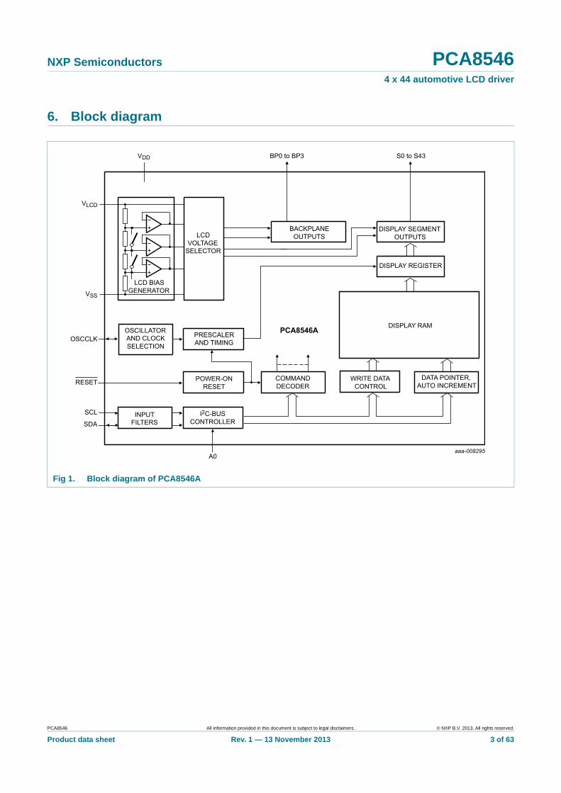
6. Block diagram
Fig 1. Block diagram of PCA8546A
PCA8546 All information provided in this document is subject to legal disclaimers. © NXP B.V. 2013. All rights reserved.
Product data sheet Rev. 1 — 13 November 2013 4 of 63
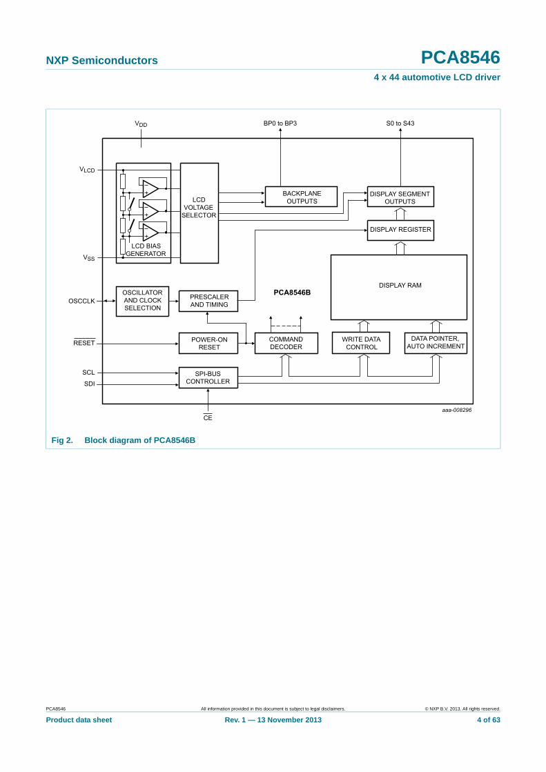
NXP Semiconductors PCA85464 x 44 automotive LCD driver
Fig 2. Block diagram of PCA8546B
xxxxxxxxxxxxxxxxxxxxx xxxxxxxxxxxxxxxxxxxxxxxxxx xxxxxxx x x x xxxxxxxxxxxxxxxxxxxxxxxxxxxxxx xxxxxxxxxxxxxxxxxxx xx xx xxxxx xxxxxxxxxxxxxxxxxxxxxxxxxxx xxxxxxxxxxxxxxxxxxx xxxxxx xxxxxxxxxxxxxxxxxxxxxxxxxxxxxxxxxxx xxxxxxxxxxxx x x xxxxxxxxxxxxxxxxxxxxx xxxxxxxxxxxxxxxxxxxxxxxxxxxxxx xxxxx xxxxxxxxxxxxxxxxxxxxxxxxxxxxxxxxxxxxxxxxxxxxxxxxxx xxxxxxxx xxxxxxxxxxxxxxxxxxxxxxxxx xxxxxxxxxxxxxxxxxxxx xxx
PC
A854
6A
ll information
provided in this do
cument is sub
ject to legal d
isclaimers.
© N
XP
B.V
. 2013. All rig
hts reserved.
Pro
du
ct data sh
eetR
ev. 1 —
13 No
vemb
er 2013 5 o
f 63
NX
P S
emico
nd
ucto
rsP
CA
85464
x 4
4 auto
mo
tive L
CD
driv
er
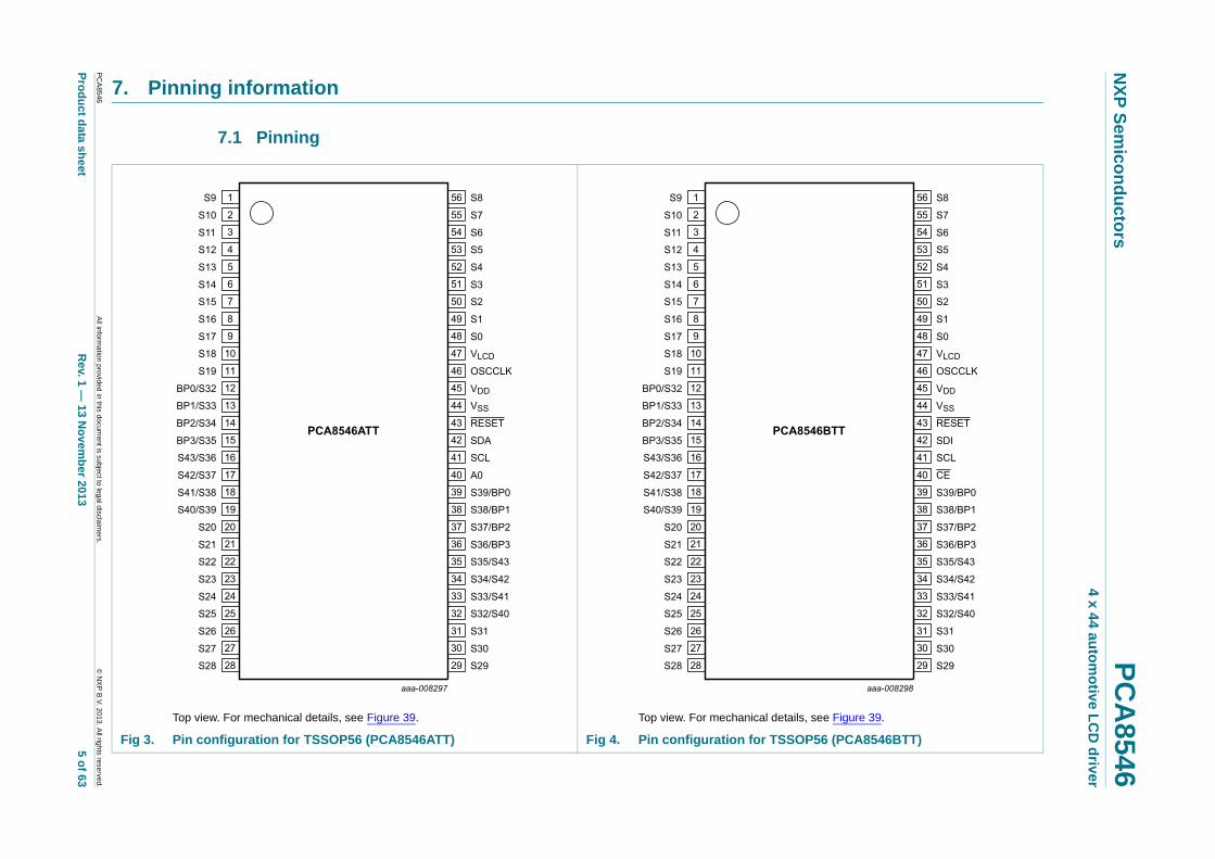
7. Pinning information
7.1 Pinning
Top view. For mechanical details, see Figure 39. Top view. For mechanical details, see Figure 39.
Fig 3. Pin configuration for TSSOP56 (PCA8546ATT) Fig 4. Pin configuration for TSSOP56 (PCA8546BTT)
PCA8546 All information provided in this document is subject to legal disclaimers. © NXP B.V. 2013. All rights reserved.
Product data sheet Rev. 1 — 13 November 2013 6 of 63
NXP Semiconductors PCA85464 x 44 automotive LCD driver
7.2 Pin description
[1] VLCD must be equal to or greater than VDD.
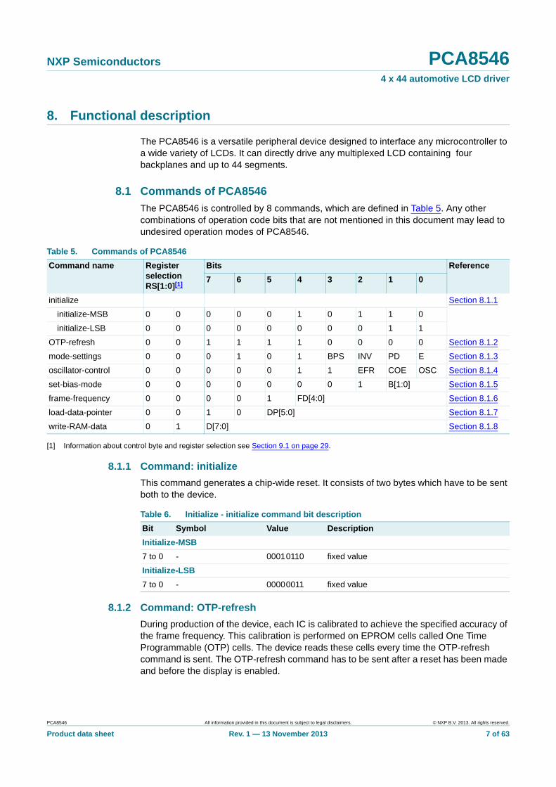
[2] Effect of backplane swapping is illustrated in Figure 5 on page 9.
[3] Bit BPS is explained in Section 8.1.3 on page 8.
Table 4. Pin description of PCA8546ATT and PCA8546BTTInput or input/output pins must always be at a defined level (VSS or VDD) unless otherwise specified.
Pin Symbol Type Description
1 to 11 S9 to S19 output LCD segment
20 to 31 S20 to S31 output LCD segment
43 RESET input active LOW reset input
44 VSS supply ground supply voltage
45 VDD supply supply voltage
46 OSCCLK input/output external clock input/internal oscillator output
47 VLCD[1] supply LCD supply voltage
48 to 56 S0 to S8 output LCD segment
Pin layout depending on backplane swap configuration[2]
BPS = 0[3] BPS = 1
12 BP0 S32 output LCD backplane/LCD segment
13 BP1 S33
14 BP2 S34
15 BP3 S35
16 S43 S36
17 S42 S37
18 S41 S38
19 S40 S39
32 S32 S40
33 S33 S41
34 S34 S42
35 S35 S43
36 S36 BP3
37 S37 BP2
38 S38 BP1
39 S39 BP0
Pin layout depending on product and bus type
PCA8546ATT PCA8546BTT
40 A0 input I2C-bus slave address selection
CE input SPI-bus chip enable - active LOW
41 SCL input I2C-bus serial clock
SCL input SPI-bus serial clock
42 SDA input/output I2C-bus serial data
SDI input SPI-bus data input
PCA8546 All information provided in this document is subject to legal disclaimers. © NXP B.V. 2013. All rights reserved.
Product data sheet Rev. 1 — 13 November 2013 7 of 63
NXP Semiconductors PCA85464 x 44 automotive LCD driver
8. Functional description
The PCA8546 is a versatile peripheral device designed to interface any microcontroller to a wide variety of LCDs. It can directly drive any multiplexed LCD containing four backplanes and up to 44 segments.
8.1 Commands of PCA8546
The PCA8546 is controlled by 8 commands, which are defined in Table 5. Any other combinations of operation code bits that are not mentioned in this document may lead to undesired operation modes of PCA8546.
[1] Information about control byte and register selection see Section 9.1 on page 29.
8.1.1 Command: initialize
This command generates a chip-wide reset. It consists of two bytes which have to be sent both to the device.
8.1.2 Command: OTP-refresh
During production of the device, each IC is calibrated to achieve the specified accuracy of the frame frequency. This calibration is performed on EPROM cells called One Time Programmable (OTP) cells. The device reads these cells every time the OTP-refresh command is sent. The OTP-refresh command has to be sent after a reset has been made and before the display is enabled.
Table 5. Commands of PCA8546
Command name Register selection RS[1:0][1]
Bits Reference
7 6 5 4 3 2 1 0
initialize Section 8.1.1
initialize-MSB 0 0 0 0 0 1 0 1 1 0
initialize-LSB 0 0 0 0 0 0 0 0 1 1
OTP-refresh 0 0 1 1 1 1 0 0 0 0 Section 8.1.2
mode-settings 0 0 0 1 0 1 BPS INV PD E Section 8.1.3
oscillator-control 0 0 0 0 0 1 1 EFR COE OSC Section 8.1.4
set-bias-mode 0 0 0 0 0 0 0 1 B[1:0] Section 8.1.5
frame-frequency 0 0 0 0 1 FD[4:0] Section 8.1.6
load-data-pointer 0 0 1 0 DP[5:0] Section 8.1.7
write-RAM-data 0 1 D[7:0] Section 8.1.8
Table 6. Initialize - initialize command bit description
Bit Symbol Value Description
Initialize-MSB
7 to 0 - 00010110 fixed value
Initialize-LSB
7 to 0 - 00000011 fixed value
PCA8546 All information provided in this document is subject to legal disclaimers. © NXP B.V. 2013. All rights reserved.
Product data sheet Rev. 1 — 13 November 2013 8 of 63
NXP Semiconductors PCA85464 x 44 automotive LCD driver
This command will be completed after a maximum of 30 ms and requires either the internal or external clock to run. If the internal oscillator is not used, then a clock must be supplied to the OSCCLK pin. If the OTP-refresh instruction is sent and no clock is present, then the request is stored until a clock is available.
Remark: It is recommended not to enter power-down mode during the OTP refresh cycle.
8.1.3 Command: mode-settings
[1] Default value.
[2] See Section 8.1.3.2.
8.1.3.1 Backplane swapping
Backplane swapping can be configured with the BPS bit (see Table 8). It moves the location of the backplane and the associated segment outputs from one side of the PCA8546 to the other. Backplane swapping is sometimes desirable to aid with the routing of PCBs that do not use multiple layers.
The BPS bit has to be set to the required value before enabling the display. Failure to do so does not damage the PCA8546 or the display, however unexpected display content may appear.
Table 7. OTP-refresh - OTP-refresh command bit description
Bit Symbol Value Description
7 to 0 - 11110000 fixed value
Table 8. Mode-settings - mode settings command bit description
Bit Symbol Value Description
7 to 4 - 0101 fixed value
3 BPS backplane swapping
0[1] backplane configuration 0
1 backplane configuration 1
2 INV set inversion mode
0[1][2] Driving scheme A: LCD line inversion mode
1 Driving scheme B: LCD frame inversion mode
1 PD set power mode
1 power-down mode; backplane and segment outputs are connected to VSS and the internal oscillator is switched off
0[1] power-up mode
0 E display switch
0[1] display disabled; backplane and segment outputs are connected to VSS
1 display enabled
PCA8546 All information provided in this document is subject to legal disclaimers. © NXP B.V. 2013. All rights reserved.
Product data sheet Rev. 1 — 13 November 2013 9 of 63
NXP Semiconductors PCA85464 x 44 automotive LCD driver
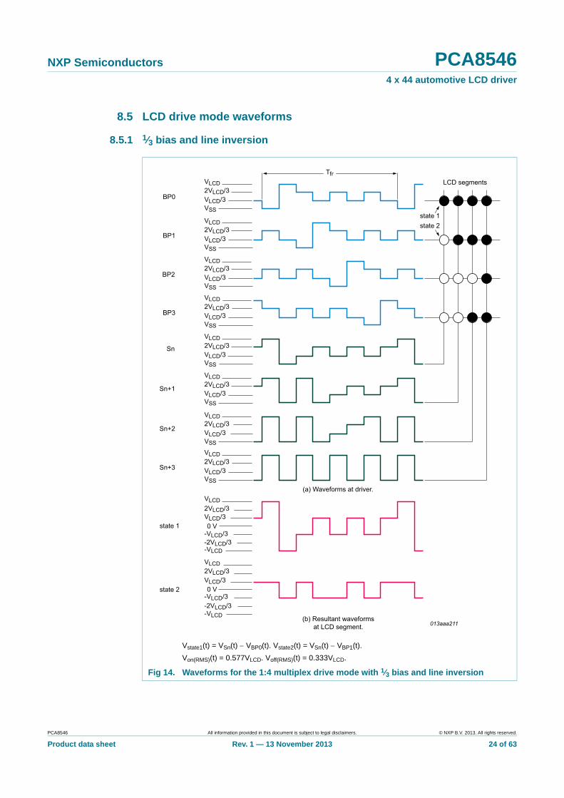
8.1.3.2 Line inversion (driving scheme A) and frame inversion (driving scheme B)
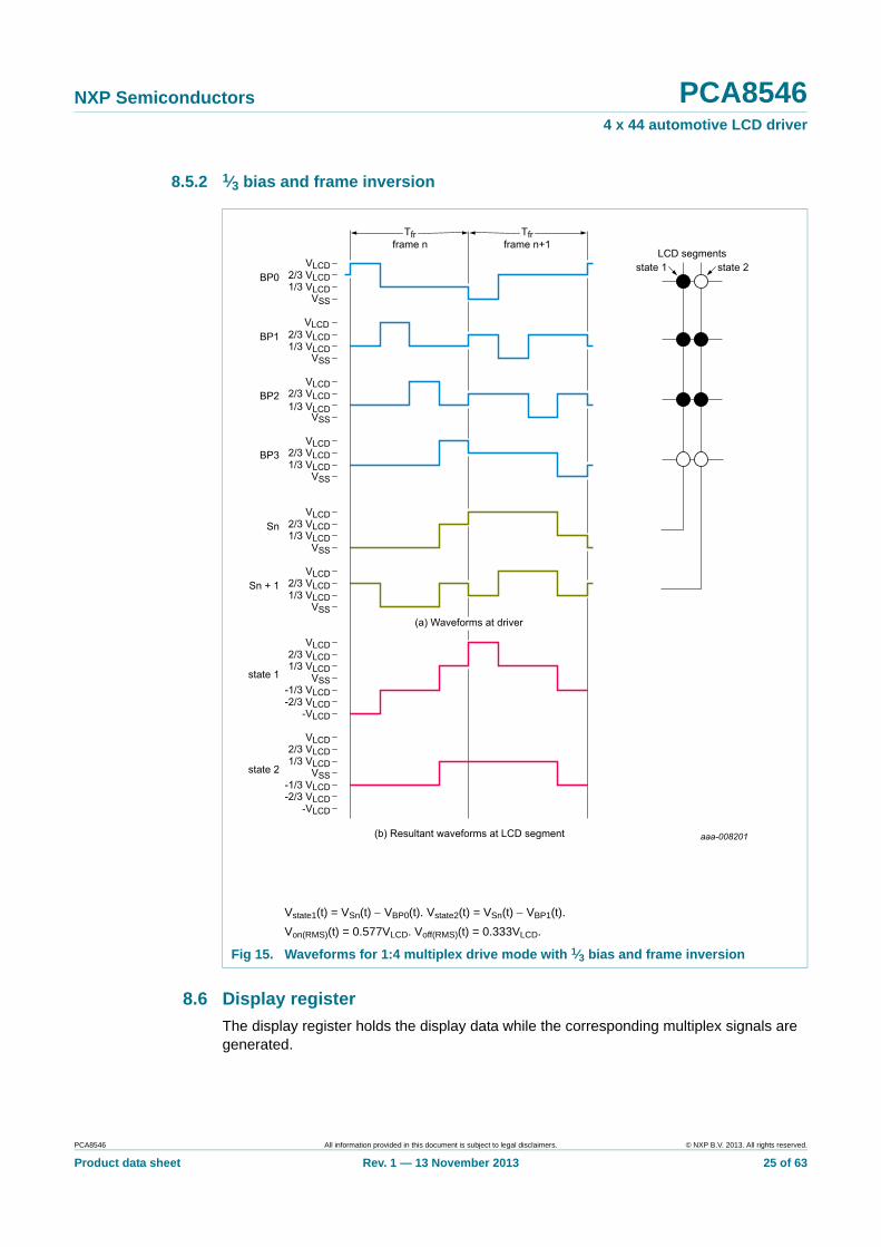
The DC offset of the voltage across the LCD is compensated over a certain period: line-wise in line inversion mode (driving scheme A) or frame-wise in frame inversion mode (driving scheme B). With the INV bit (see Table 8), the compensation mode can be switched.
In frame inversion mode, the DC value is compensated across two frames and not within one frame. Changing the inversion mode to frame inversion reduces the power consumption; therefore it is useful when power consumption is a key point in the application.
Frame inversion may not be suitable for all applications. The RMS voltage across a segment is better defined; however, since the switching frequency is reduced, there is possibility for flicker to occur.
The waveforms of Figure 14 shows the line inversion mode. Figure 15 shows the frame inversion mode.
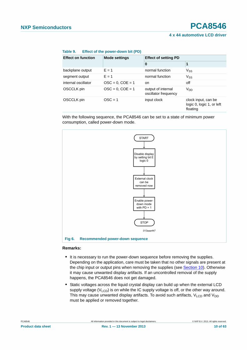
8.1.3.3 Power-down mode
The power-down bit (PD) allows the PCA8546 to be put in a minimum power configuration. To avoid display artifacts, enter power-down only after the display has been switched off by setting bit E to logic 0. During power-down, the internal oscillator is switched off.
Fig 5. Effect of backplane swapping
PCA8546 All information provided in this document is subject to legal disclaimers. © NXP B.V. 2013. All rights reserved.
Product data sheet Rev. 1 — 13 November 2013 10 of 63
NXP Semiconductors PCA85464 x 44 automotive LCD driver
With the following sequence, the PCA8546 can be set to a state of minimum power consumption, called power-down mode.
Remarks:
• It is necessary to run the power-down sequence before removing the supplies. Depending on the application, care must be taken that no other signals are present at the chip input or output pins when removing the supplies (see Section 10). Otherwise it may cause unwanted display artifacts. If an uncontrolled removal of the supply happens, the PCA8546 does not get damaged.
• Static voltages across the liquid crystal display can build up when the external LCD supply voltage (VLCD) is on while the IC supply voltage is off, or the other way around. This may cause unwanted display artifacts. To avoid such artifacts, VLCD and VDD must be applied or removed together.
Table 9. Effect of the power-down bit (PD)
Effect on function Mode settings Effect of setting PD
0 1
backplane output E = 1 normal function VSS
segment output E = 1 normal function VSS
internal oscillator OSC = 0, COE = 1 on off
OSCCLK pin OSC = 0, COE = 1 output of internal oscillator frequency
VDD
OSCCLK pin OSC = 1 input clock clock input, can be logic 0, logic 1, or left floating
Fig 6. Recommended power-down sequence
PCA8546 All information provided in this document is subject to legal disclaimers. © NXP B.V. 2013. All rights reserved.
Product data sheet Rev. 1 — 13 November 2013 11 of 63
NXP Semiconductors PCA85464 x 44 automotive LCD driver
• A clock signal must always be supplied to the device when the display is active. Removing the clock may freeze the LCD in a DC state, which is not suitable for the liquid crystal. First disable the display and afterwards remove the clock signal.
8.1.3.4 Display enable
The display enable bit (E) is used to enable and disable the display. When the display is disabled, all LCD outputs go to VSS. This function is implemented to ensure that no voltage can be induced on the LCD outputs as it may lead to unwanted displays of segments.
Recommended start-up sequences are found in Section 8.2.3
Remark: Display enable is not synchronized to an LCD frame boundary. Therefore using this function to flash a display for prolonged periods is not recommended due to the possible build-up of DC voltages on the display.
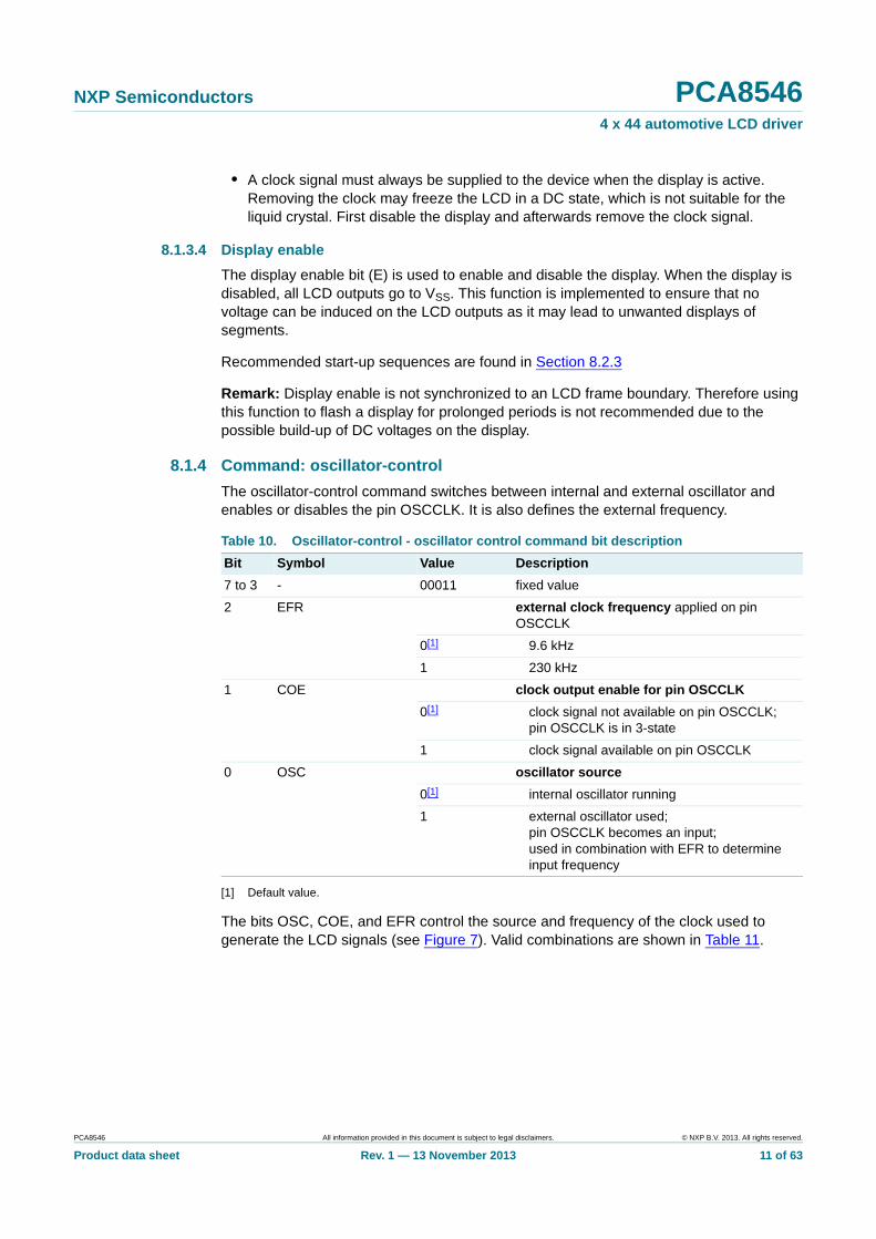
8.1.4 Command: oscillator-control
The oscillator-control command switches between internal and external oscillator and enables or disables the pin OSCCLK. It is also defines the external frequency.
[1] Default value.
The bits OSC, COE, and EFR control the source and frequency of the clock used to generate the LCD signals (see Figure 7). Valid combinations are shown in Table 11.
Table 10. Oscillator-control - oscillator control command bit description
Bit Symbol Value Description
7 to 3 - 00011 fixed value
2 EFR external clock frequency applied on pin OSCCLK
0[1] 9.6 kHz
1 230 kHz
1 COE clock output enable for pin OSCCLK
0[1] clock signal not available on pin OSCCLK;pin OSCCLK is in 3-state
1 clock signal available on pin OSCCLK
0 OSC oscillator source
0[1] internal oscillator running
1 external oscillator used;pin OSCCLK becomes an input;used in combination with EFR to determine input frequency
PCA8546 All information provided in this document is subject to legal disclaimers. © NXP B.V. 2013. All rights reserved.
Product data sheet Rev. 1 — 13 November 2013 12 of 63
NXP Semiconductors PCA85464 x 44 automotive LCD driver
8.1.4.1 Oscillator
The system is designed to operate from a 9.6 kHz or a 230 kHz clock. This clock can be sourced internally or externally. The internal logic and LCD drive signals of the PCA8546 are timed either by the internal oscillator or from the clock externally supplied.
Internal clock: When the internal oscillator is used, all LCD signals are generated from it. The oscillator runs at nominal 230 kHz. The relationship between this frequency and the LCD frame frequency is detailed in Section 8.1.6. Control over the internal oscillator is made with the OSC bit (see Section 8.1.4).
It is possible to make the internal oscillator signal available on pin OSCCLK by using the oscillator-control command (see Table 10) and configuring the clock output enable (COE) bit. If not required, the pin OSCCLK should be left open or connected to VSS. At power-on the signal at pin OSCCLK is disabled and pin OSCCLK is in 3-state.
Clock output is only valid when using the internal oscillator. The signal appears on the OSCCLK pin.
An intermediate clock frequency is available at the OSCCLK pin. The duty cycle of this clock varies with the chosen divide ratio.
(1) Can only be used with the internal oscillator (OSC = 0).
(2) Can only be used with an external oscillator (OSC = 1).
(3) Nominal value for divide factor q is 24; source clock is 230 kHz (see Section 8.1.6).
Fig 7. Oscillator selection
Table 11. Valid combinations of bits OSC, EFR, and COE
OSC COE EFR OSCCLK pin Clock source
0 0 not used inactive;may be left floating
internal oscillator used
0 1 not used output of internal oscillator frequency (prescaler)
internal oscillator used
1 not used 0 9.6 kHz input OSCCLK pin
1 not used 1 230 kHz input OSCCLK pin
Table 12. Typical use of bits OSC, EFR, and COE
Usage OSC COE EFR
LCD with internal oscillator 0 0 not used
LCD with external oscillator (230 kHz) 1 not used 1
LCD with external oscillator (9.6 kHz) 1 not used 0
PCA8546 All information provided in this document is subject to legal disclaimers. © NXP B.V. 2013. All rights reserved.
Product data sheet Rev. 1 — 13 November 2013 13 of 63
NXP Semiconductors PCA85464 x 44 automotive LCD driver
[1] When RESET is active, the pin OSCCLK is in 3-state.
[2] In this state, an external clock may be applied, but it is not a requirement.
[3] 9.6 kHz is the nominal frequency with q = 24, see Table 14.
External clock: In applications where an external clock must be applied to the PCA8546, bit OSC (see Table 10) has to be set logic 1. In this case pin OSCCLK becomes an input.
The OSCCLK signal must switch between the VSS and the VDD voltage supplied to the chip.
The EFR bit determines the external clock frequency (230 kHz or 9.6 kHz). The clock frequency (fclk(ext)) in turn determines the LCD frame frequency, see Table 14.
Remark: If an external clock is used, then this clock signal must always be supplied to the device when the display is on. Removing the clock may freeze the LCD in a DC state which damages the LCD material.
8.1.4.2 Timing and frame frequency
The timing of the PCA8546 organizes the internal data flow of the device. This includes the transfer of display data from the display RAM to the display segment outputs. The timing also generates the LCD frame frequency which it derives as an integer division of the clock frequency (see Table 14). The frame frequency is a fixed division of the internal clock or of the frequency applied to pin OSCCLK when an external clock is used.
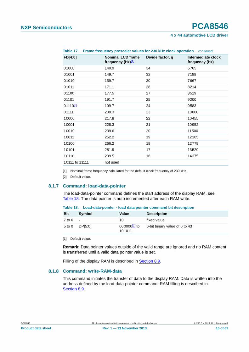
[1] Other values of the frame frequency prescaler see Table 17.
When the internal clock is used, or an external clock with EFR = 1, the LCD frame frequency can be programmed by software in steps of approximately 10 Hz in the range of 60 Hz to 300 Hz (see Table 17). Furthermore the internal oscillator is factory calibrated, see Table 32 on page 42.
8.1.5 Command: set-bias-mode
The set-bias-mode command allows setting the bias level.
Table 13. OSCCLK pin state depending on configuration
PD OSC COE EFR OSCCLK pin[1]
power-down n.a. off n.a. 3-state[2]
power-down n.a. on n.a. VDD
power-up internal oscillator off n.a. 3-state
on n.a. 9.6 kHz output[3]
external oscillator n.a. 9.6 kHz 9.6 kHz input
230 kHz 230 kHz input
Table 14. LCD frame frequencies
Frame frequency Typical external frequency (Hz)
Nominal frame frequency (Hz)
EFR bit Value of q[1]
9600 200 0 -
230000 200 1 24
ffr LCD fclk ext
48-----------------=
ffr LCD fclk ext
48 q-----------------=
PCA8546 All information provided in this document is subject to legal disclaimers. © NXP B.V. 2013. All rights reserved.
Product data sheet Rev. 1 — 13 November 2013 14 of 63
NXP Semiconductors PCA85464 x 44 automotive LCD driver
[1] Default value.
8.1.6 Command: frame-frequency
With the frame-frequency command, the frame frequency for the display can be configured. The clock frequency determines the frame frequency.
When using an external clock it can be either a 230 kHz or a 9.6 kHz clock signal. The EFR bit (see Table 10) has to be set according to the external clock frequency.
When EFR is set to 9.6 kHz, then the LCD frame frequency is calculated with Equation 1:
(1)
When EFR is set to 230 kHz, then the LCD frame frequency is calculated with Equation 2:
(2)
where q is the frequency divide factor (see Table 17).
Remark: fclk(ext) is the external input clock frequency to pin OSCCLK.
When the internal oscillator is used, the intermediate frequency may be output on the OSCCLK pin. Its frequency is given in Table 17.
Table 15. Set-bias-mode - set bias mode command bit description
Bit Symbol Value Description
7 to 2 - 000001 fixed value
1 to 0 B[1:0] 00[1]. 01 1⁄4 bias
11 1⁄3 bias
10 1⁄2 bias
Table 16. Frame-frequency - frame frequency and output clock frequency command bit description
Bit Symbol Value Description
7 to 5 - 001 fixed value
4 to 0 FD[4:0] see Table 17 frequency prescaler
Table 17. Frame frequency prescaler values for 230 kHz clock operation
FD[4:0] Nominal LCD frame frequency (Hz)[1]
Divide factor, q Intermediate clock frequency (Hz)
00000 59.9 80 2875
00001 70.5 68 3382
00010 79.9 60 3833
00011 90.4 53 4340
00100 99.8 48 4792
00101 108.9 44 5227
00110 119.8 40 5750
00111 129.5 37 6216
ffr LCD fclk ext
48-----------------=
ffr LCD fclk ext
48 q-----------------=
PCA8546 All information provided in this document is subject to legal disclaimers. © NXP B.V. 2013. All rights reserved.
Product data sheet Rev. 1 — 13 November 2013 15 of 63
NXP Semiconductors PCA85464 x 44 automotive LCD driver
[1] Nominal frame frequency calculated for the default clock frequency of 230 kHz.
[2] Default value.
8.1.7 Command: load-data-pointer
The load-data-pointer command defines the start address of the display RAM, see Table 18. The data pointer is auto incremented after each RAM write.
[1] Default value.
Remark: Data pointer values outside of the valid range are ignored and no RAM content is transferred until a valid data pointer value is set.
Filling of the display RAM is described in Section 8.9.
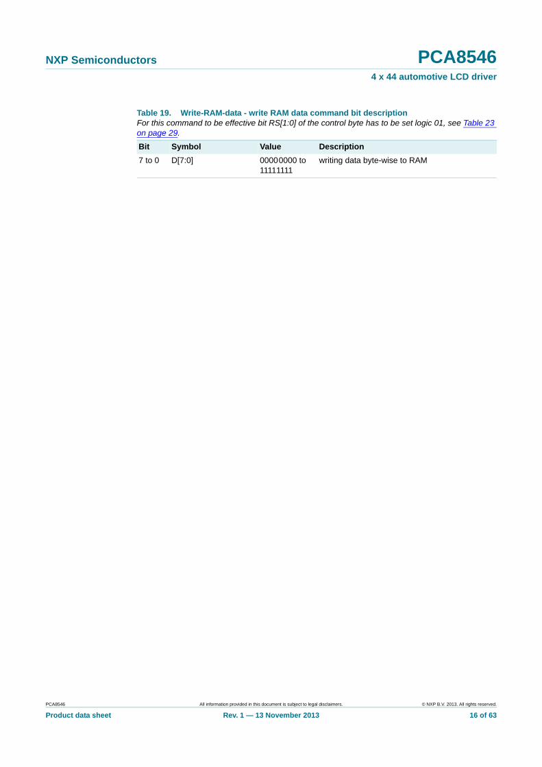
8.1.8 Command: write-RAM-data
This command initiates the transfer of data to the display RAM. Data is written into the address defined by the load-data-pointer command. RAM filling is described in Section 8.9.
01000 140.9 34 6765
01001 149.7 32 7188
01010 159.7 30 7667
01011 171.1 28 8214
01100 177.5 27 8519
01101 191.7 25 9200
01110[2] 199.7 24 9583
01111 208.3 23 10000
10000 217.8 22 10455
10001 228.3 21 10952
10010 239.6 20 11500
10011 252.2 19 12105
10100 266.2 18 12778
10101 281.9 17 13529
10110 299.5 16 14375
10111 to 11111 not used
Table 17. Frame frequency prescaler values for 230 kHz clock operation …continued
FD[4:0] Nominal LCD frame frequency (Hz)[1]
Divide factor, q Intermediate clock frequency (Hz)
Table 18. Load-data-pointer - load data pointer command bit description
Bit Symbol Value Description
7 to 6 - 10 fixed value
5 to 0 DP[5:0] 000000[1] to 101011
6-bit binary value of 0 to 43
PCA8546 All information provided in this document is subject to legal disclaimers. © NXP B.V. 2013. All rights reserved.
Product data sheet Rev. 1 — 13 November 2013 16 of 63
NXP Semiconductors PCA85464 x 44 automotive LCD driver
Table 19. Write-RAM-data - write RAM data command bit descriptionFor this command to be effective bit RS[1:0] of the control byte has to be set logic 01, see Table 23 on page 29.
Bit Symbol Value Description
7 to 0 D[7:0] 00000000 to 11111111
writing data byte-wise to RAM
PCA8546 All information provided in this document is subject to legal disclaimers. © NXP B.V. 2013. All rights reserved.
Product data sheet Rev. 1 — 13 November 2013 17 of 63
NXP Semiconductors PCA85464 x 44 automotive LCD driver
8.2 Start-up and shut-down
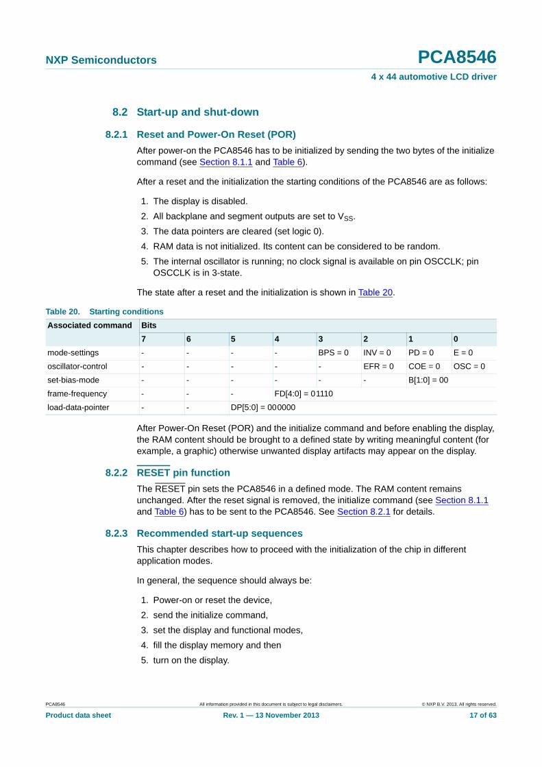
8.2.1 Reset and Power-On Reset (POR)
After power-on the PCA8546 has to be initialized by sending the two bytes of the initialize command (see Section 8.1.1 and Table 6).
After a reset and the initialization the starting conditions of the PCA8546 are as follows:
1. The display is disabled.
2. All backplane and segment outputs are set to VSS.
3. The data pointers are cleared (set logic 0).
4. RAM data is not initialized. Its content can be considered to be random.
5. The internal oscillator is running; no clock signal is available on pin OSCCLK; pin OSCCLK is in 3-state.
The state after a reset and the initialization is shown in Table 20.
After Power-On Reset (POR) and the initialize command and before enabling the display, the RAM content should be brought to a defined state by writing meaningful content (for example, a graphic) otherwise unwanted display artifacts may appear on the display.
8.2.2 RESET pin function
The RESET pin sets the PCA8546 in a defined mode. The RAM content remains unchanged. After the reset signal is removed, the initialize command (see Section 8.1.1 and Table 6) has to be sent to the PCA8546. See Section 8.2.1 for details.
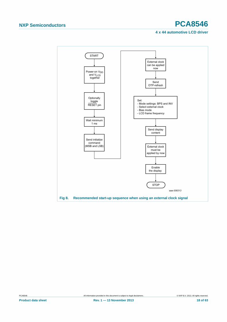
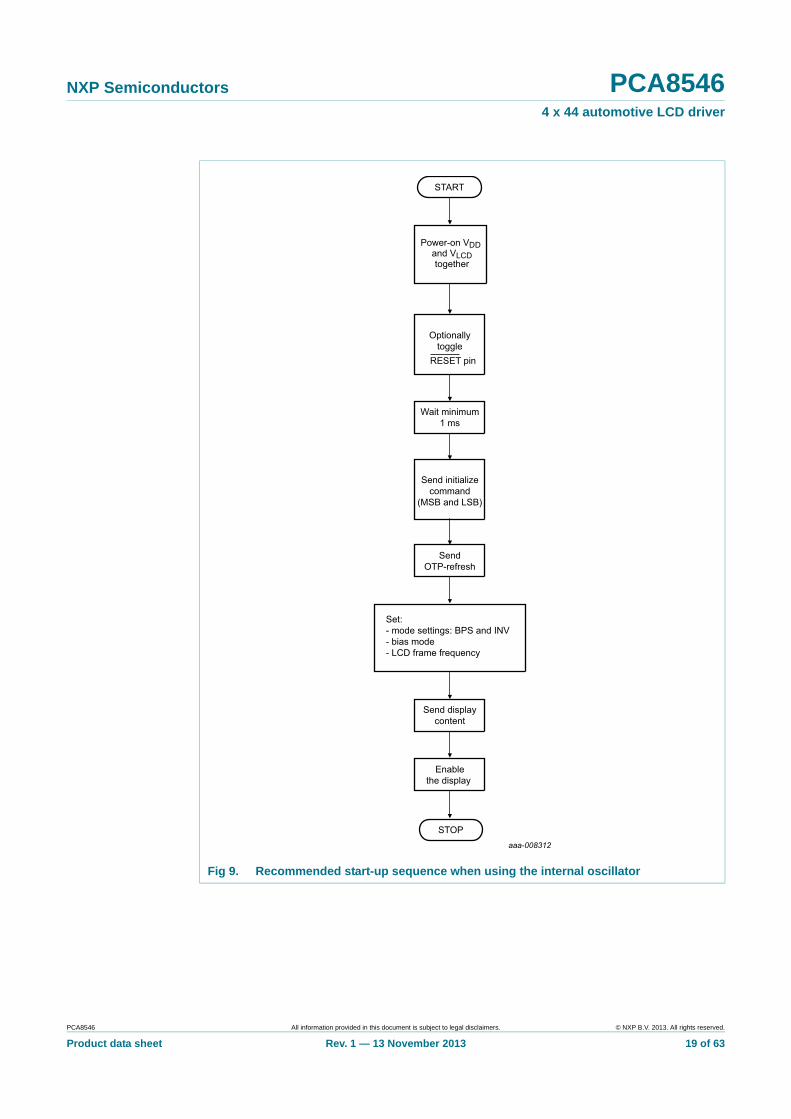
8.2.3 Recommended start-up sequences
This chapter describes how to proceed with the initialization of the chip in different application modes.
In general, the sequence should always be:
1. Power-on or reset the device,
2. send the initialize command,
3. set the display and functional modes,
4. fill the display memory and then
5. turn on the display.
Table 20. Starting conditions
Associated command Bits
7 6 5 4 3 2 1 0
mode-settings - - - - BPS = 0 INV = 0 PD = 0 E = 0
oscillator-control - - - - - EFR = 0 COE = 0 OSC = 0
set-bias-mode - - - - - - B[1:0] = 00
frame-frequency - - - FD[4:0] = 01110
load-data-pointer - - DP[5:0] = 000000
PCA8546 All information provided in this document is subject to legal disclaimers. © NXP B.V. 2013. All rights reserved.
Product data sheet Rev. 1 — 13 November 2013 18 of 63
NXP Semiconductors PCA85464 x 44 automotive LCD driver
Fig 8. Recommended start-up sequence when using an external clock signal
PCA8546 All information provided in this document is subject to legal disclaimers. © NXP B.V. 2013. All rights reserved.
Product data sheet Rev. 1 — 13 November 2013 19 of 63
NXP Semiconductors PCA85464 x 44 automotive LCD driver
Fig 9. Recommended start-up sequence when using the internal oscillator
PCA8546 All information provided in this document is subject to legal disclaimers. © NXP B.V. 2013. All rights reserved.
Product data sheet Rev. 1 — 13 November 2013 20 of 63
NXP Semiconductors PCA85464 x 44 automotive LCD driver
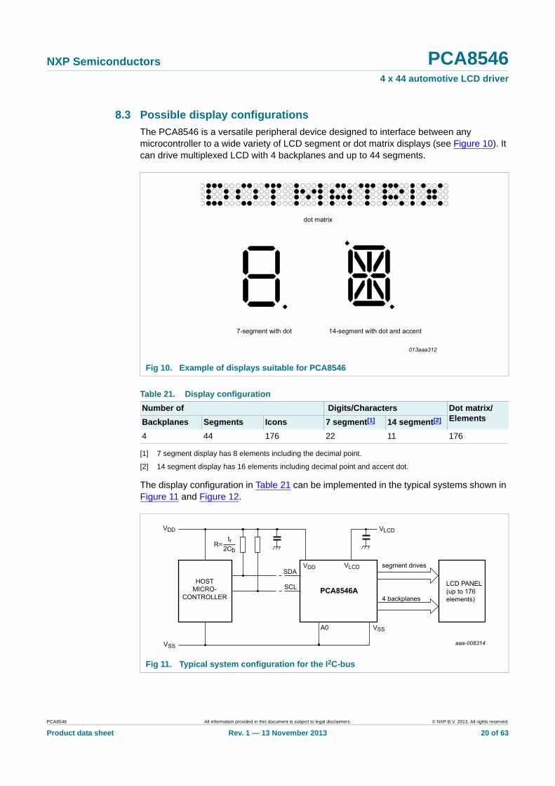
8.3 Possible display configurations
The PCA8546 is a versatile peripheral device designed to interface between any microcontroller to a wide variety of LCD segment or dot matrix displays (see Figure 10). It can drive multiplexed LCD with 4 backplanes and up to 44 segments.
[1] 7 segment display has 8 elements including the decimal point.
[2] 14 segment display has 16 elements including decimal point and accent dot.
The display configuration in Table 21 can be implemented in the typical systems shown in Figure 11 and Figure 12.
Fig 10. Example of displays suitable for PCA8546
Table 21. Display configuration
Number of Digits/Characters Dot matrix/ ElementsBackplanes Segments Icons 7 segment[1] 14 segment[2]
4 44 176 22 11 176
Fig 11. Typical system configuration for the I2C-bus
PCA8546 All information provided in this document is subject to legal disclaimers. © NXP B.V. 2013. All rights reserved.
Product data sheet Rev. 1 — 13 November 2013 21 of 63
NXP Semiconductors PCA85464 x 44 automotive LCD driver
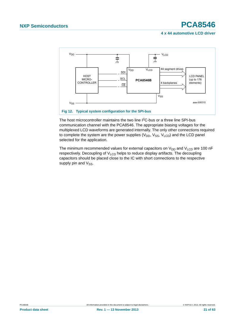
The host microcontroller maintains the two line I2C-bus or a three line SPI-bus communication channel with the PCA8546. The appropriate biasing voltages for the multiplexed LCD waveforms are generated internally. The only other connections required to complete the system are the power supplies (VDD, VSS, VLCD) and the LCD panel selected for the application.
The minimum recommended values for external capacitors on VDD and VLCD are 100 nF respectively. Decoupling of VLCD helps to reduce display artifacts. The decoupling capacitors should be placed close to the IC with short connections to the respective supply pin and VSS.
Fig 12. Typical system configuration for the SPI-bus
PCA8546 All information provided in this document is subject to legal disclaimers. © NXP B.V. 2013. All rights reserved.
Product data sheet Rev. 1 — 13 November 2013 22 of 63
NXP Semiconductors PCA85464 x 44 automotive LCD driver
8.4 LCD voltage selector
The LCD voltage selector coordinates the multiplexing of the LCD in accordance with the selected LCD drive configuration. The operation of the voltage selector is controlled by the set-bias-mode command (see Table 15).
Fractional LCD biasing voltages are obtained from an internal voltage divider. The biasing configurations, the biasing characteristics as functions of VLCD and the resulting discrimination ratios (D), are given in Table 22.
Discrimination is a term which is defined as the ratio of the on and off RMS voltage across a segment. It can be thought of as a measurement of contrast.
[1] Determined from Equation 5.
[2] Determined from Equation 4.
[3] In these examples, the discrimination factor and hence the contrast ratios are smaller. The advantage of these LCD drive modes is a reduction of the LCD voltage VLCD.
A practical value for VLCD is determined by equating Voff(RMS) with a defined LCD threshold voltage (Vth(off)), typically when the LCD exhibits approximately 10 % contrast.
Bias is calculated by , where the values for a are
a = 1 for 1⁄2 bias
a = 2 for 1⁄3 bias
a = 3 for 1⁄4 bias
The RMS on-state voltage (Von(RMS)) for the LCD is calculated with Equation 3
(3)
where VLCD is the resultant voltage at the LCD segment and where the value for n is
n = 4 for 1:4 multiplex drive
The RMS off-state voltage (Voff(RMS)) for the LCD is calculated with Equation 4:
(4)
Discrimination is the ratio of Von(RMS) to Voff(RMS) and is determined from Equation 5:
Table 22. Preferred LCD drive modes: summary of characteristics
LCD multiplex drive mode
Number of: LCD biasconfiguration
[1]VLCD
[2]
Backplanes Levels
1:4 [3] 4 3 1⁄2 0.433 0.661 1.527 2.309Voff(RMS)
1:4 4 4 1⁄3 0.333 0.577 1.732 3.0Voff(RMS)
1:4 [3] 4 5 1⁄4 0.331 0.545 1.646 3.024Voff(RMS)
Voff RMS VLCD
-----------------------Von RMS
VLCD---------------------- D
Von RMS Voff RMS -----------------------=
11 a+-------------
Von RMS a2 2a n+ +
n 1 a+ 2------------------------------VLCD
=
Voff RMS a2 2a– n+
n 1 a+ 2------------------------------VLCD
=
PCA8546 All information provided in this document is subject to legal disclaimers. © NXP B.V. 2013. All rights reserved.
Product data sheet Rev. 1 — 13 November 2013 23 of 63
NXP Semiconductors PCA85464 x 44 automotive LCD driver
(5)
VLCD is sometimes referred to as the LCD operating voltage.
8.4.1 Electro-optical performance
Suitable values for Von(RMS) and Voff(RMS) are dependent on the LCD liquid used. The RMS voltage, at which a pixel gets switched on or off, determine the transmissibility of the pixel.
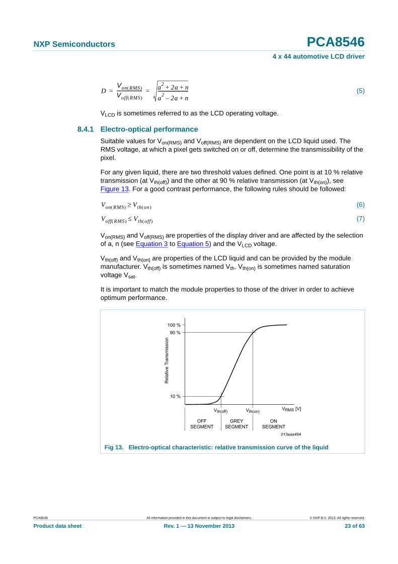
For any given liquid, there are two threshold values defined. One point is at 10 % relative transmission (at Vth(off)) and the other at 90 % relative transmission (at Vth(on)), see Figure 13. For a good contrast performance, the following rules should be followed:
(6)
(7)
Von(RMS) and Voff(RMS) are properties of the display driver and are affected by the selection of a, n (see Equation 3 to Equation 5) and the VLCD voltage.
Vth(off) and Vth(on) are properties of the LCD liquid and can be provided by the module manufacturer. Vth(off) is sometimes named Vth. Vth(on) is sometimes named saturation voltage Vsat.
It is important to match the module properties to those of the driver in order to achieve optimum performance.
DVon RMS
Voff RMS ----------------------- a
22a n+ +
a2
2a– n+---------------------------= =
Fig 13. Electro-optical characteristic: relative transmission curve of the liquid
Von RMS Vth on
Voff RMS Vth off
PCA8546 All information provided in this document is subject to legal disclaimers. © NXP B.V. 2013. All rights reserved.
Product data sheet Rev. 1 — 13 November 2013 24 of 63
NXP Semiconductors PCA85464 x 44 automotive LCD driver
8.5 LCD drive mode waveforms
8.5.1 1⁄3 bias and line inversion
Vstate1(t) = VSn(t) VBP0(t). Vstate2(t) = VSn(t) VBP1(t).
Von(RMS)(t) = 0.577VLCD. Voff(RMS)(t) = 0.333VLCD.
Fig 14. Waveforms for the 1:4 multiplex drive mode with 1⁄3 bias and line inversion
PCA8546 All information provided in this document is subject to legal disclaimers. © NXP B.V. 2013. All rights reserved.
Product data sheet Rev. 1 — 13 November 2013 25 of 63
NXP Semiconductors PCA85464 x 44 automotive LCD driver
8.5.2 1⁄3 bias and frame inversion
8.6 Display register
The display register holds the display data while the corresponding multiplex signals are generated.
Vstate1(t) = VSn(t) VBP0(t). Vstate2(t) = VSn(t) VBP1(t).
Von(RMS)(t) = 0.577VLCD. Voff(RMS)(t) = 0.333VLCD.
Fig 15. Waveforms for 1:4 multiplex drive mode with 1⁄3 bias and frame inversion
PCA8546 All information provided in this document is subject to legal disclaimers. © NXP B.V. 2013. All rights reserved.
Product data sheet Rev. 1 — 13 November 2013 26 of 63
NXP Semiconductors PCA85464 x 44 automotive LCD driver
8.7 Backplane outputs
The LCD drive section includes four backplane outputs: BP0 to BP3 which must be connected directly to the LCD.
8.8 Segment outputs
The LCD drive section includes up to 44 segment outputs (S0 to S43) which must be connected directly to the LCD. The segment output signals are generated based on the data resident in the display register. When less segment outputs are required, the unused segment outputs must be left open-circuit.
8.9 Display RAM
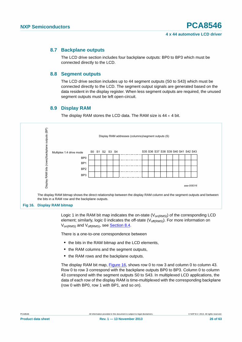
The display RAM stores the LCD data. The RAM size is 44 4 bit.
Logic 1 in the RAM bit map indicates the on-state (Von(RMS)) of the corresponding LCD element; similarly, logic 0 indicates the off-state (Voff(RMS)). For more information on Von(RMS) and Voff(RMS), see Section 8.4.
There is a one-to-one correspondence between
• the bits in the RAM bitmap and the LCD elements,
• the RAM columns and the segment outputs,
• the RAM rows and the backplane outputs.
The display RAM bit map, Figure 16, shows row 0 to row 3 and column 0 to column 43. Row 0 to row 3 correspond with the backplane outputs BP0 to BP3. Column 0 to column 43 correspond with the segment outputs S0 to S43. In multiplexed LCD applications, the data of each row of the display RAM is time-multiplexed with the corresponding backplane (row 0 with BP0, row 1 with BP1, and so on).
The display RAM bitmap shows the direct relationship between the display RAM column and the segment outputs and between the bits in a RAM row and the backplane outputs.
Fig 16. Display RAM bitmap
PCA8546 All information provided in this document is subject to legal disclaimers. © NXP B.V. 2013. All rights reserved.
Product data sheet Rev. 1 — 13 November 2013 27 of 63
NXP Semiconductors PCA85464 x 44 automotive LCD driver
8.9.1 Data pointer
The addressing mechanism for the display RAM is realized using the data pointer. This allows the loading of an individual display data byte, or a series of display data bytes, into any location of the display RAM. The sequence commences with the initialization of the data pointer by the load-data-pointer command (see Table 18).
Following this command, an arriving data byte is stored starting at the display RAM address indicated by the data pointer.
The data pointer is automatically incremented. That is, after each byte is stored, the contents of the data pointer are incremented by two.
When the address counter reaches the end of the RAM, it stops incrementing after the last byte is transmitted. Redundant bits of the last byte and subsequent bytes transmitted are discarded until the pointer is reset. To send new RAM data, the data pointer must be reset.
If an I2C-bus or SPI-bus data access is terminated early, then the state of the data pointer is unknown. The data pointer must then be rewritten before further RAM accesses.
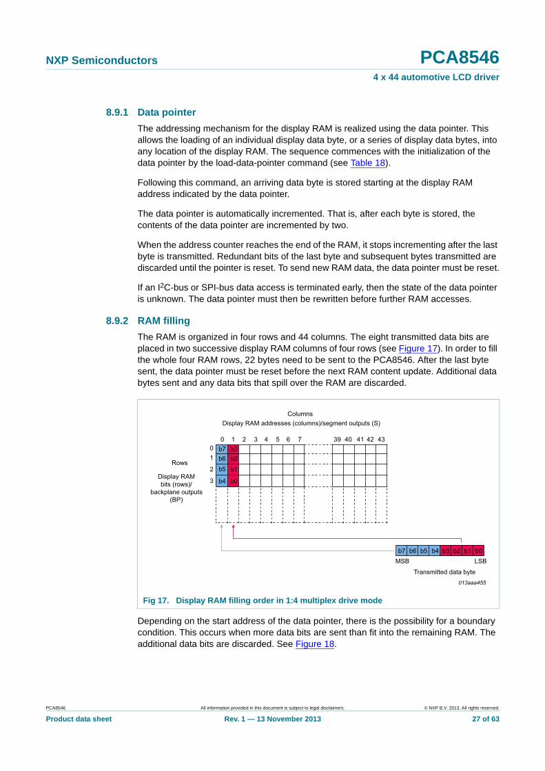
8.9.2 RAM filling
The RAM is organized in four rows and 44 columns. The eight transmitted data bits are placed in two successive display RAM columns of four rows (see Figure 17). In order to fill the whole four RAM rows, 22 bytes need to be sent to the PCA8546. After the last byte sent, the data pointer must be reset before the next RAM content update. Additional data bytes sent and any data bits that spill over the RAM are discarded.
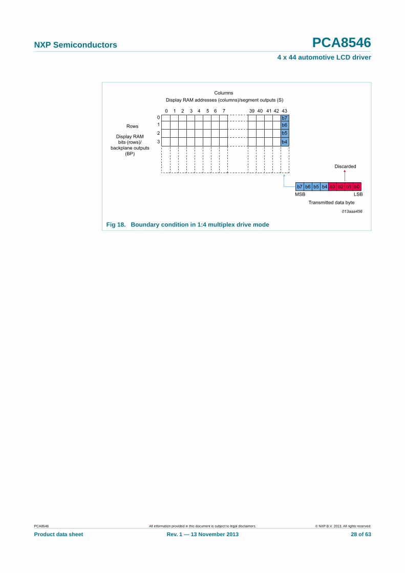
Depending on the start address of the data pointer, there is the possibility for a boundary condition. This occurs when more data bits are sent than fit into the remaining RAM. The additional data bits are discarded. See Figure 18.
Fig 17. Display RAM filling order in 1:4 multiplex drive mode
PCA8546 All information provided in this document is subject to legal disclaimers. © NXP B.V. 2013. All rights reserved.
Product data sheet Rev. 1 — 13 November 2013 28 of 63
NXP Semiconductors PCA85464 x 44 automotive LCD driver
Fig 18. Boundary condition in 1:4 multiplex drive mode
PCA8546 All information provided in this document is subject to legal disclaimers. © NXP B.V. 2013. All rights reserved.
Product data sheet Rev. 1 — 13 November 2013 29 of 63
NXP Semiconductors PCA85464 x 44 automotive LCD driver
9. Bus interfaces
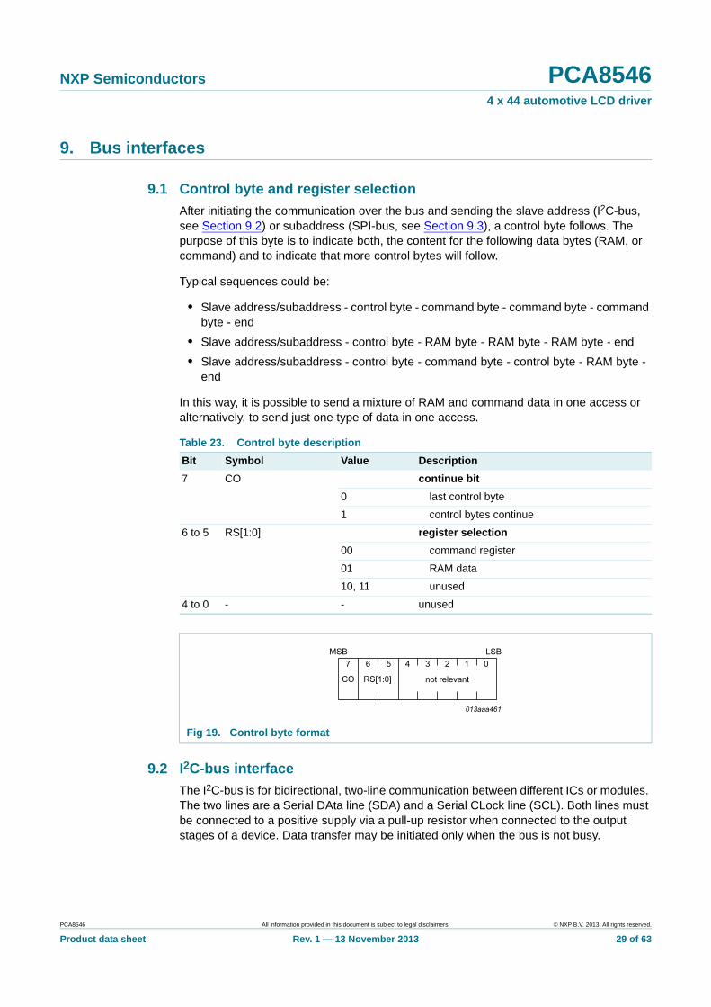
9.1 Control byte and register selection
After initiating the communication over the bus and sending the slave address (I2C-bus, see Section 9.2) or subaddress (SPI-bus, see Section 9.3), a control byte follows. The purpose of this byte is to indicate both, the content for the following data bytes (RAM, or command) and to indicate that more control bytes will follow.
Typical sequences could be:
• Slave address/subaddress - control byte - command byte - command byte - command byte - end
• Slave address/subaddress - control byte - RAM byte - RAM byte - RAM byte - end
• Slave address/subaddress - control byte - command byte - control byte - RAM byte - end
In this way, it is possible to send a mixture of RAM and command data in one access or alternatively, to send just one type of data in one access.
9.2 I2C-bus interface
The I2C-bus is for bidirectional, two-line communication between different ICs or modules. The two lines are a Serial DAta line (SDA) and a Serial CLock line (SCL). Both lines must be connected to a positive supply via a pull-up resistor when connected to the output stages of a device. Data transfer may be initiated only when the bus is not busy.
Table 23. Control byte description
Bit Symbol Value Description
7 CO continue bit
0 last control byte
1 control bytes continue
6 to 5 RS[1:0] register selection
00 command register
01 RAM data
10, 11 unused
4 to 0 - - unused
Fig 19. Control byte format
PCA8546 All information provided in this document is subject to legal disclaimers. © NXP B.V. 2013. All rights reserved.
Product data sheet Rev. 1 — 13 November 2013 30 of 63
NXP Semiconductors PCA85464 x 44 automotive LCD driver
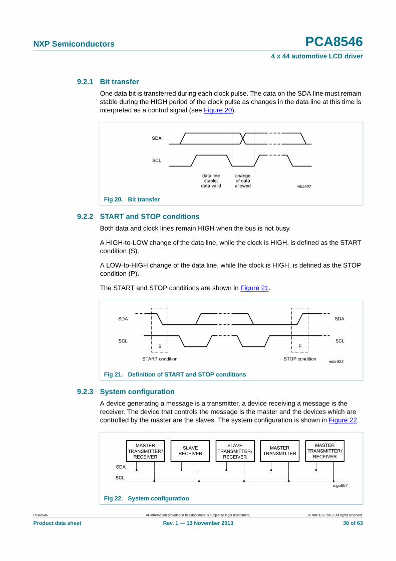
9.2.1 Bit transfer
One data bit is transferred during each clock pulse. The data on the SDA line must remain stable during the HIGH period of the clock pulse as changes in the data line at this time is interpreted as a control signal (see Figure 20).
9.2.2 START and STOP conditions
Both data and clock lines remain HIGH when the bus is not busy.
A HIGH-to-LOW change of the data line, while the clock is HIGH, is defined as the START condition (S).
A LOW-to-HIGH change of the data line, while the clock is HIGH, is defined as the STOP condition (P).
The START and STOP conditions are shown in Figure 21.
9.2.3 System configuration
A device generating a message is a transmitter, a device receiving a message is the receiver. The device that controls the message is the master and the devices which are controlled by the master are the slaves. The system configuration is shown in Figure 22.
Fig 20. Bit transfer
Fig 21. Definition of START and STOP conditions
Fig 22. System configuration
PCA8546 All information provided in this document is subject to legal disclaimers. © NXP B.V. 2013. All rights reserved.
Product data sheet Rev. 1 — 13 November 2013 31 of 63
NXP Semiconductors PCA85464 x 44 automotive LCD driver
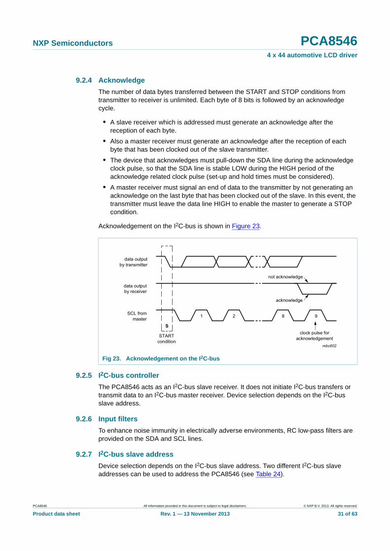
9.2.4 Acknowledge
The number of data bytes transferred between the START and STOP conditions from transmitter to receiver is unlimited. Each byte of 8 bits is followed by an acknowledge cycle.
• A slave receiver which is addressed must generate an acknowledge after the reception of each byte.
• Also a master receiver must generate an acknowledge after the reception of each byte that has been clocked out of the slave transmitter.
• The device that acknowledges must pull-down the SDA line during the acknowledge clock pulse, so that the SDA line is stable LOW during the HIGH period of the acknowledge related clock pulse (set-up and hold times must be considered).
• A master receiver must signal an end of data to the transmitter by not generating an acknowledge on the last byte that has been clocked out of the slave. In this event, the transmitter must leave the data line HIGH to enable the master to generate a STOP condition.
Acknowledgement on the I2C-bus is shown in Figure 23.
9.2.5 I2C-bus controller
The PCA8546 acts as an I2C-bus slave receiver. It does not initiate I2C-bus transfers or transmit data to an I2C-bus master receiver. Device selection depends on the I2C-bus slave address.
9.2.6 Input filters
To enhance noise immunity in electrically adverse environments, RC low-pass filters are provided on the SDA and SCL lines.
9.2.7 I2C-bus slave address
Device selection depends on the I2C-bus slave address. Two different I2C-bus slave addresses can be used to address the PCA8546 (see Table 24).
Fig 23. Acknowledgement on the I2C-bus
PCA8546 All information provided in this document is subject to legal disclaimers. © NXP B.V. 2013. All rights reserved.
Product data sheet Rev. 1 — 13 November 2013 32 of 63
NXP Semiconductors PCA85464 x 44 automotive LCD driver
The least significant bit of the slave address byte is bit R/W (see Table 25).
Bit 1 of the slave address is defined by connecting the input A0 to either VSS (logic 0) or VDD (logic 1). Therefore, two instances of PCA8546 can be distinguished on the same I2C-bus.
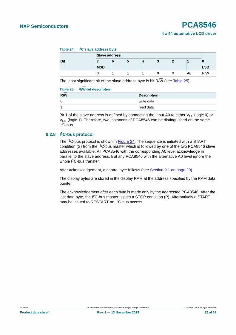
9.2.8 I2C-bus protocol
The I2C-bus protocol is shown in Figure 24. The sequence is initiated with a START condition (S) from the I2C-bus master which is followed by one of the two PCA8546 slave addresses available. All PCA8546 with the corresponding A0 level acknowledge in parallel to the slave address. But any PCA8546 with the alternative A0 level ignore the whole I2C-bus transfer.
After acknowledgement, a control byte follows (see Section 9.1 on page 29).
The display bytes are stored in the display RAM at the address specified by the RAM data pointer.
The acknowledgement after each byte is made only by the addressed PCA8546. After the last data byte, the I2C-bus master issues a STOP condition (P). Alternatively a START may be issued to RESTART an I2C-bus access.
Table 24. I2C slave address byte
Slave address
Bit 7 6 5 4 3 2 1 0
MSB LSB
0 1 1 1 0 0 A0 R/W
Table 25. R/W-bit description
R/W Description
0 write data
1 read data
PCA8546 All information provided in this document is subject to legal disclaimers. © NXP B.V. 2013. All rights reserved.
Product data sheet Rev. 1 — 13 November 2013 33 of 63
NXP Semiconductors PCA85464 x 44 automotive LCD driver
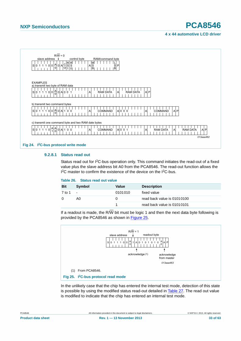
9.2.8.1 Status read out
Status read out for I2C-bus operation only. This command initiates the read-out of a fixed value plus the slave address bit A0 from the PCA8546. The read-out function allows the I2C master to confirm the existence of the device on the I2C-bus.
If a readout is made, the R/W bit must be logic 1 and then the next data byte following is provided by the PCA8546 as shown in Figure 25.
In the unlikely case that the chip has entered the internal test mode, detection of this state is possible by using the modified status read-out detailed in Table 27. The read out value is modified to indicate that the chip has entered an internal test mode.
Fig 24. I2C-bus protocol write mode
Table 26. Status read out value
Bit Symbol Value Description
7 to 1 - 0101010 fixed value
0 A0 0 read back value is 01010100
1 read back value is 01010101
(1) From PCA8546.
Fig 25. I2C-bus protocol read mode
PCA8546 All information provided in this document is subject to legal disclaimers. © NXP B.V. 2013. All rights reserved.
Product data sheet Rev. 1 — 13 November 2013 34 of 63
NXP Semiconductors PCA85464 x 44 automotive LCD driver
EMC detection: The PCA8546 is ruggedized against EMC susceptibility; however it is not possible to cover all cases. To detect if a severe EMC event has occurred, it is possible to check the responsiveness of the device by reading its register.
9.3 SPI-bus interface
Data transfer to the device is made via a 3 line SPI-bus (see Table 28). There is no output data line. The SPI-bus is initialized whenever the chip enable line pin CE is inactive.
[1] The chip enable must not be wired permanently LOW.
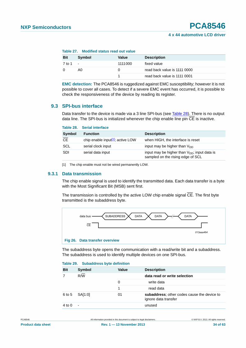
9.3.1 Data transmission
The chip enable signal is used to identify the transmitted data. Each data transfer is a byte with the Most Significant Bit (MSB) sent first.
The transmission is controlled by the active LOW chip enable signal CE. The first byte transmitted is the subaddress byte.
The subaddress byte opens the communication with a read/write bit and a subaddress. The subaddress is used to identify multiple devices on one SPI-bus.
Table 27. Modified status read out value
Bit Symbol Value Description
7 to 1 - 1111000 fixed value
0 A0 0 read back value is 1111 0000
1 read back value is 1111 0001
Table 28. Serial interface
Symbol Function Description
CE chip enable input[1]; active LOW when HIGH, the interface is reset
SCL serial clock input input may be higher than VDD
SDI serial data input input may be higher than VDD; input data is sampled on the rising edge of SCL
Fig 26. Data transfer overview
Table 29. Subaddress byte definition
Bit Symbol Value Description
7 R/W data read or write selection
0 write data
1 read data
6 to 5 SA[1:0] 01 subaddress; other codes cause the device to ignore data transfer
4 to 0 - unused
PCA8546 All information provided in this document is subject to legal disclaimers. © NXP B.V. 2013. All rights reserved.
Product data sheet Rev. 1 — 13 November 2013 35 of 63
NXP Semiconductors PCA85464 x 44 automotive LCD driver
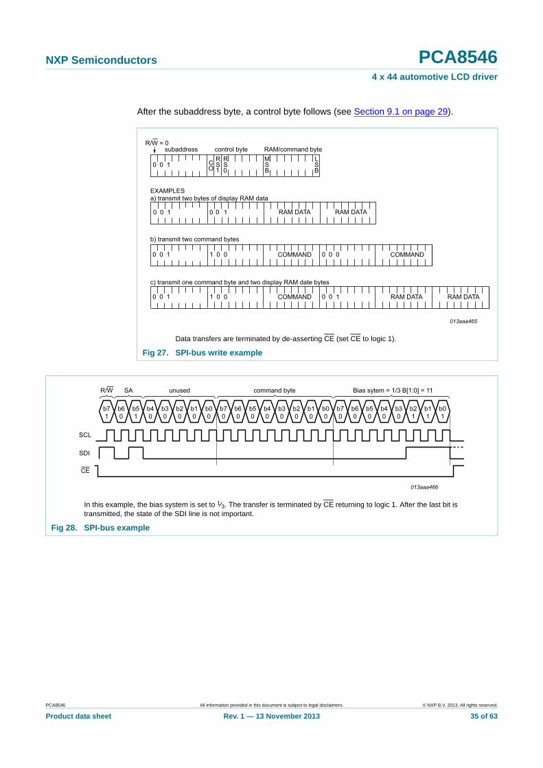
After the subaddress byte, a control byte follows (see Section 9.1 on page 29).
Data transfers are terminated by de-asserting CE (set CE to logic 1).
Fig 27. SPI-bus write example
In this example, the bias system is set to 1⁄3. The transfer is terminated by CE returning to logic 1. After the last bit is transmitted, the state of the SDI line is not important.
Fig 28. SPI-bus example
PCA8546 All information provided in this document is subject to legal disclaimers. © NXP B.V. 2013. All rights reserved.
Product data sheet Rev. 1 — 13 November 2013 36 of 63
NXP Semiconductors PCA85464 x 44 automotive LCD driver
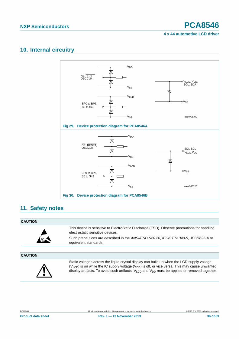
10. Internal circuitry
11. Safety notes
Fig 29. Device protection diagram for PCA8546A
Fig 30. Device protection diagram for PCA8546B
CAUTION
This device is sensitive to ElectroStatic Discharge (ESD). Observe precautions for handling electrostatic sensitive devices.
Such precautions are described in the ANSI/ESD S20.20, IEC/ST 61340-5, JESD625-A or equivalent standards.
CAUTION
Static voltages across the liquid crystal display can build up when the LCD supply voltage (VLCD) is on while the IC supply voltage (VDD) is off, or vice versa. This may cause unwanted display artifacts. To avoid such artifacts, VLCD and VDD must be applied or removed together.
PCA8546 All information provided in this document is subject to legal disclaimers. © NXP B.V. 2013. All rights reserved.
Product data sheet Rev. 1 — 13 November 2013 37 of 63
NXP Semiconductors PCA85464 x 44 automotive LCD driver
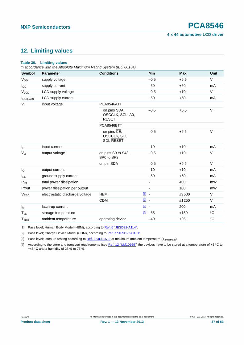
12. Limiting values
[1] Pass level; Human Body Model (HBM), according to Ref. 6 “JESD22-A114”.
[2] Pass level; Charge Device Model (CDM), according to Ref. 7 “JESD22-C101”.
[3] Pass level; latch-up testing according to Ref. 8 “JESD78” at maximum ambient temperature (Tamb(max)).
[4] According to the store and transport requirements (see Ref. 12 “UM10569”) the devices have to be stored at a temperature of +8 C to +45 C and a humidity of 25 % to 75 %.
Table 30. Limiting valuesIn accordance with the Absolute Maximum Rating System (IEC 60134).
Symbol Parameter Conditions Min Max Unit
VDD supply voltage 0.5 +6.5 V
IDD supply current 50 +50 mA
VLCD LCD supply voltage 0.5 +10 V
IDD(LCD) LCD supply current 50 +50 mA
VI input voltage PCA8546ATT
on pins SDA, OSCCLK, SCL, A0, RESET
0.5 +6.5 V
PCA8546BTT
on pins CE, OSCCLK, SCL, SDI, RESET
0.5 +6.5 V
II input current 10 +10 mA
VO output voltage on pins S0 to S43, BP0 to BP3
0.5 +10 V
on pin SDA 0.5 +6.5 V
IO output current 10 +10 mA
ISS ground supply current 50 +50 mA
Ptot total power dissipation - 400 mW
P/out power dissipation per output - 100 mW
VESD electrostatic discharge voltage HBM [1] - 3500 V
CDM [2] - 1250 V
Ilu latch-up current [3] - 200 mA
Tstg storage temperature [4] 65 +150 C
Tamb ambient temperature operating device 40 +95 C
PCA8546 All information provided in this document is subject to legal disclaimers. © NXP B.V. 2013. All rights reserved.
Product data sheet Rev. 1 — 13 November 2013 38 of 63
NXP Semiconductors PCA85464 x 44 automotive LCD driver
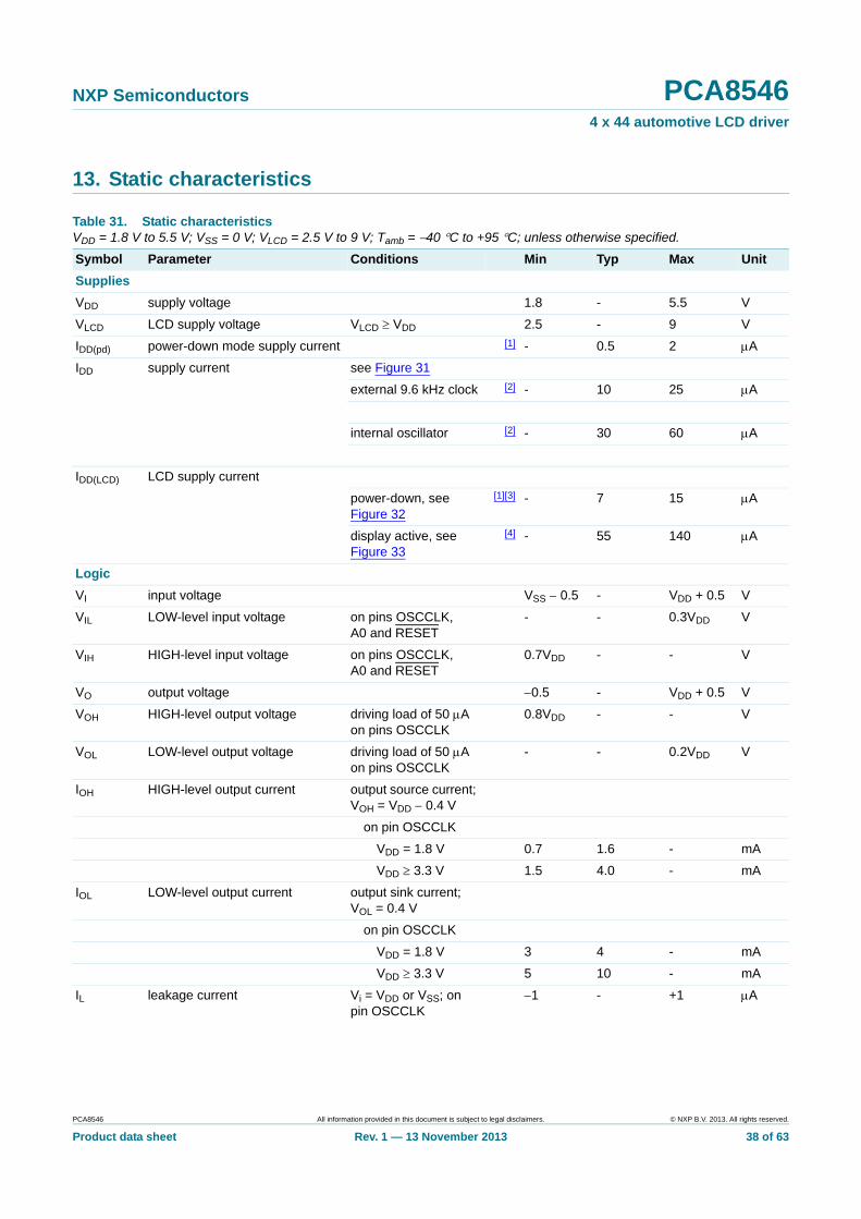
13. Static characteristics
Table 31. Static characteristicsVDD = 1.8 V to 5.5 V; VSS = 0 V; VLCD = 2.5 V to 9 V; Tamb = 40 C to +95 C; unless otherwise specified.
Symbol Parameter Conditions Min Typ Max Unit
Supplies
VDD supply voltage 1.8 - 5.5 V
VLCD LCD supply voltage VLCD VDD 2.5 - 9 V
IDD(pd) power-down mode supply current [1] - 0.5 2 A
IDD supply current see Figure 31
external 9.6 kHz clock [2] - 10 25 A
internal oscillator [2] - 30 60 A
IDD(LCD) LCD supply current
power-down, see Figure 32
[1][3] - 7 15 A
display active, see Figure 33
[4] - 55 140 A
Logic
VI input voltage VSS 0.5 - VDD + 0.5 V
VIL LOW-level input voltage on pins OSCCLK, A0 and RESET
- - 0.3VDD V
VIH HIGH-level input voltage on pins OSCCLK, A0 and RESET
0.7VDD - - V
VO output voltage 0.5 - VDD + 0.5 V
VOH HIGH-level output voltage driving load of 50 A on pins OSCCLK
0.8VDD - - V
VOL LOW-level output voltage driving load of 50 A on pins OSCCLK
- - 0.2VDD V
IOH HIGH-level output current output source current; VOH = VDD 0.4 V
on pin OSCCLK
VDD = 1.8 V 0.7 1.6 - mA
VDD 3.3 V 1.5 4.0 - mA
IOL LOW-level output current output sink current; VOL = 0.4 V
on pin OSCCLK
VDD = 1.8 V 3 4 - mA
VDD 3.3 V 5 10 - mA
IL leakage current Vi = VDD or VSS; on pin OSCCLK
1 - +1 A
PCA8546 All information provided in this document is subject to legal disclaimers. © NXP B.V. 2013. All rights reserved.
Product data sheet Rev. 1 — 13 November 2013 39 of 63
NXP Semiconductors PCA85464 x 44 automotive LCD driver
[1] Power-down mode is enabled; I2C-bus or SPI-bus inactive.
[2] 1⁄4 bias; display enabled; LCD outputs are open circuit; RAM is all written with logic 1; inputs at VSS or VDD; default display prescale factor; I2C-bus or SPI-bus inactive.
[3] Strongly linked to VLCD voltage. See Figure 32.
[4] 1⁄4 bias; display enabled; LCD outputs are open circuit; RAM is all written with logic 1; default display prescale factor.
[5] The I2C-bus interface of PCA8546 is 5 V tolerant.
[6] Variation between any two backplanes on a given voltage level; static measured.
[7] Variation between any two segments on a given voltage level; static measured.
[8] Outputs measured one at a time.
I2C-bus[5]
On pins SCL and SDA
VI input voltage VSS 0.5 - 5.5 V
VIL LOW-level input voltage - - 0.3VDD V
VIH HIGH-level input voltage 0.7VDD - - V
VO output voltage 0.5 - +5.5 V
IL leakage current VI = VDD or VSS 1 - +1 A
On pin SDA
IOL LOW-level output current output sink current
VDD = 1.8 V 3 5.5 - mA
VDD = 3.3 V 5 9 - mA
SPI-bus
VI input voltage
on pin SCL VSS 0.5 - 5.5 V
on pins CE and SDI VSS 0.5 - VDD + 0.5 V
On pins SCL, CE and SDI
VIL LOW-level input voltage - - 0.3VDD V
VIH HIGH-level input voltage 0.7VDD - - V
IL leakage current VI = VDD or VSS 1 - +1 A
LCD outputs
VO output voltage variation
on pins BP0 to BP3 [6] - 2.5 +10 mV
on pins S0 to S43 [7] - 2.5 +10 mV
RO output resistance
VLCD = 7 V; on pins BP0 to BP3
[8] - 0.9 5.0 k
VLCD = 7 V; on pins S0 to S43
[8] - 1.5 6.0 k
Table 31. Static characteristics …continuedVDD = 1.8 V to 5.5 V; VSS = 0 V; VLCD = 2.5 V to 9 V; Tamb = 40 C to +95 C; unless otherwise specified.
Symbol Parameter Conditions Min Typ Max Unit
PCA8546 All information provided in this document is subject to legal disclaimers. © NXP B.V. 2013. All rights reserved.
Product data sheet Rev. 1 — 13 November 2013 40 of 63
NXP Semiconductors PCA85464 x 44 automotive LCD driver
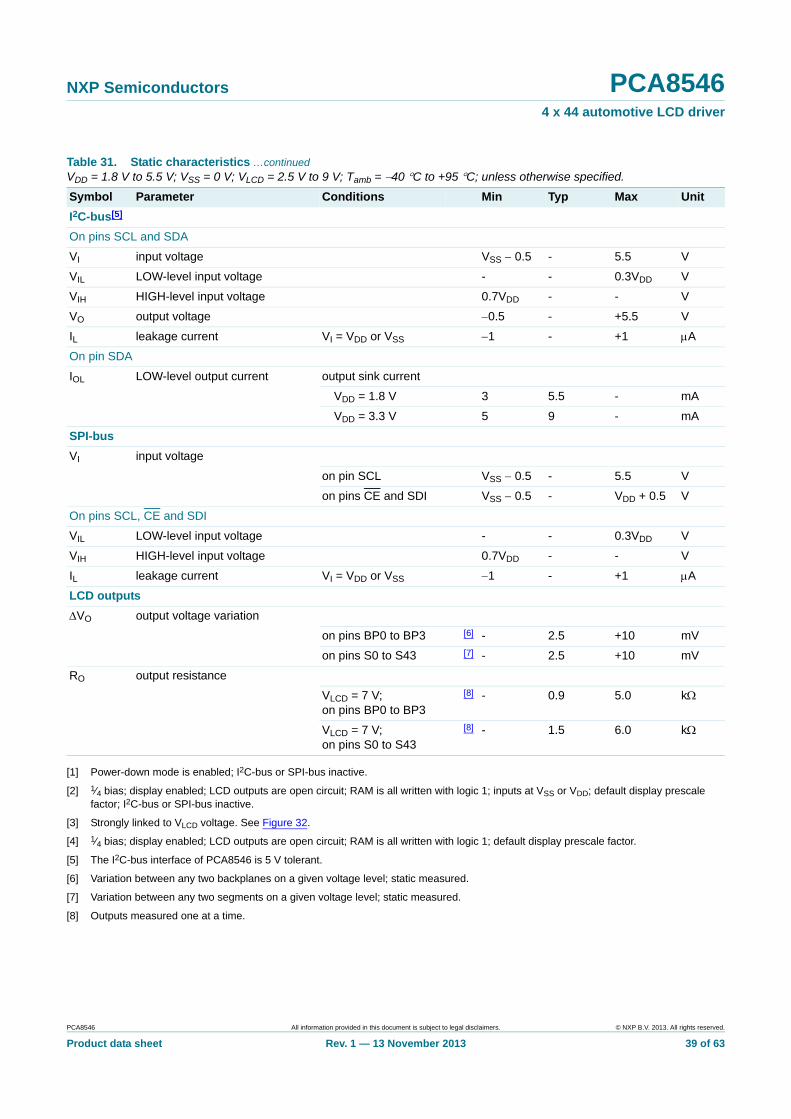
1⁄4 bias; internal oscillator; display enabled; LCD outputs are open circuit; RAM is all written with logic 1; inputs at VSS or VDD; default display prescale factor; I2C-bus or SPI-bus inactive. Typical is defined at VDD = 3.3 V, 25 C.
Fig 31. Typical IDD with respect to temperature
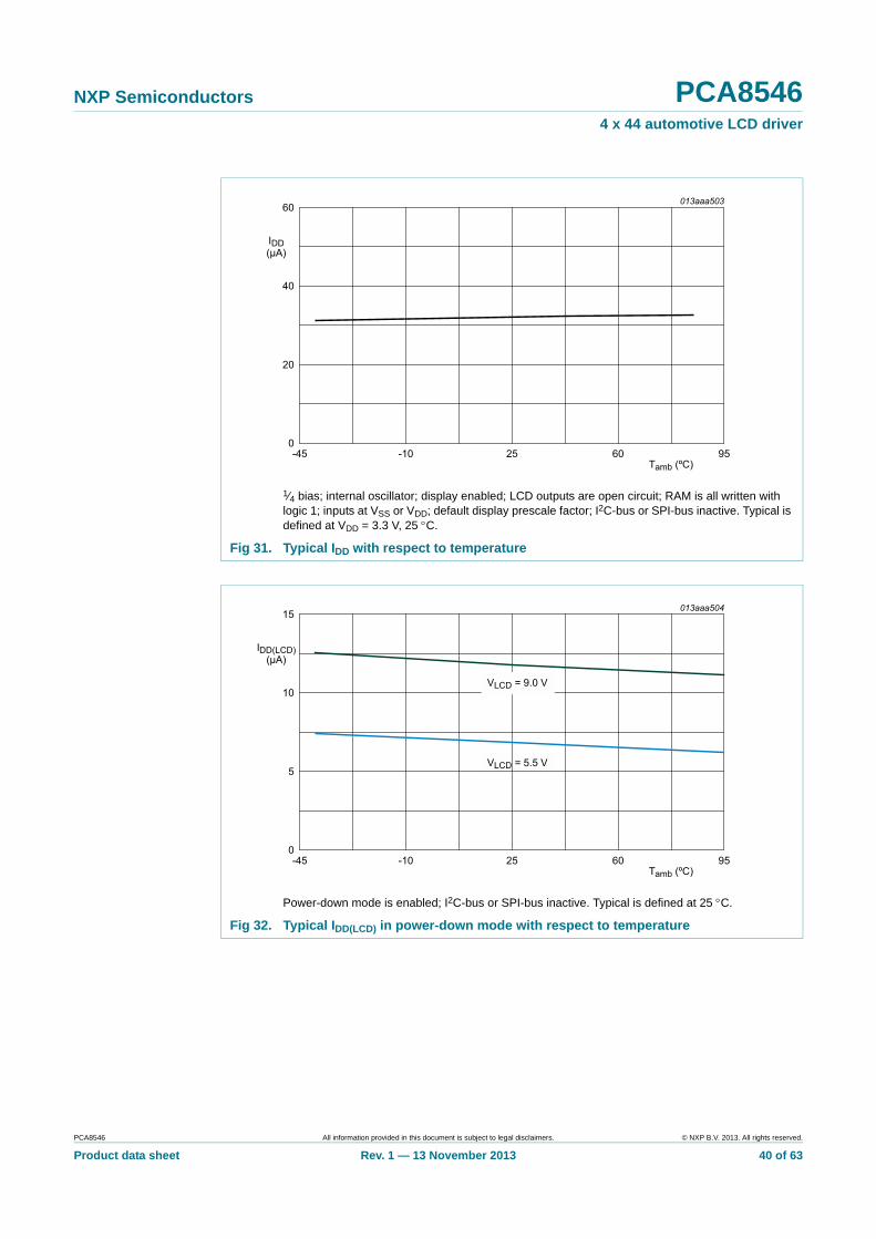
Power-down mode is enabled; I2C-bus or SPI-bus inactive. Typical is defined at 25 C.
Fig 32. Typical IDD(LCD) in power-down mode with respect to temperature
PCA8546 All information provided in this document is subject to legal disclaimers. © NXP B.V. 2013. All rights reserved.
Product data sheet Rev. 1 — 13 November 2013 41 of 63
NXP Semiconductors PCA85464 x 44 automotive LCD driver
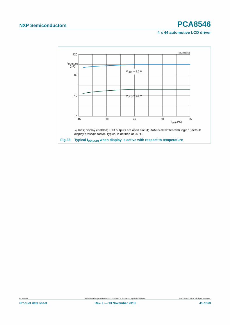
1⁄4 bias; display enabled; LCD outputs are open circuit; RAM is all written with logic 1; default display prescale factor. Typical is defined at 25 C.
Fig 33. Typical IDD(LCD) when display is active with respect to temperature
PCA8546 All information provided in this document is subject to legal disclaimers. © NXP B.V. 2013. All rights reserved.
Product data sheet Rev. 1 — 13 November 2013 42 of 63
NXP Semiconductors PCA85464 x 44 automotive LCD driver
14. Dynamic characteristics
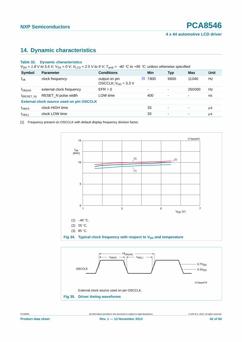
[1] Frequency present on OSCCLK with default display frequency division factor.
Table 32. Dynamic characteristicsVDD = 1.8 V to 5.5 V; VSS = 0 V; VLCD = 2.5 V to 9 V; Tamb = 40 C to +95 C; unless otherwise specified.
Symbol Parameter Conditions Min Typ Max Unit
fclk clock frequency output on pin OSCCLK; VDD = 3.3 V
[1] 7800 9600 11040 Hz
fclk(ext) external clock frequency EFR = 0 - - 250000 Hz
t(RESET_N) RESET_N pulse width LOW time 400 - - ns
External clock source used on pin OSCCLK
tclk(H) clock HIGH time 33 - - s
tclk(L) clock LOW time 33 - - s
(1) 40 C.
(2) 25 C.
(3) 85 C.
Fig 34. Typical clock frequency with respect to VDD and temperature
External clock source used on pin OSCCLK.
Fig 35. Driver timing waveforms
PCA8546 All information provided in this document is subject to legal disclaimers. © NXP B.V. 2013. All rights reserved.
Product data sheet Rev. 1 — 13 November 2013 43 of 63
NXP Semiconductors PCA85464 x 44 automotive LCD driver
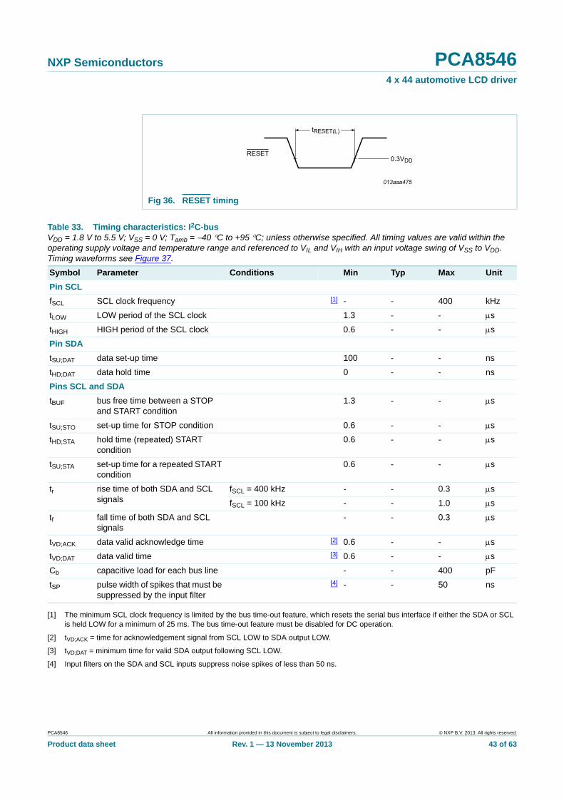
[1] The minimum SCL clock frequency is limited by the bus time-out feature, which resets the serial bus interface if either the SDA or SCL is held LOW for a minimum of 25 ms. The bus time-out feature must be disabled for DC operation.
[2] tVD;ACK = time for acknowledgement signal from SCL LOW to SDA output LOW.
[3] tVD;DAT = minimum time for valid SDA output following SCL LOW.
[4] Input filters on the SDA and SCL inputs suppress noise spikes of less than 50 ns.
Fig 36. RESET timing
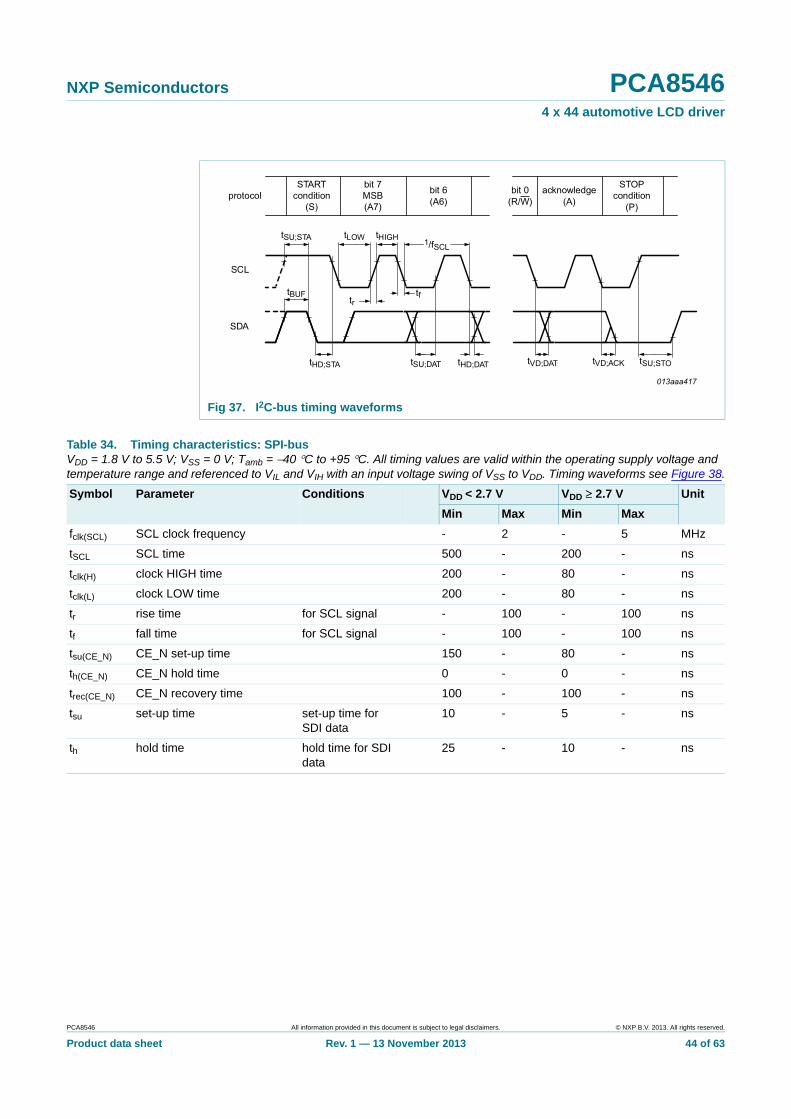
Table 33. Timing characteristics: I2C-busVDD = 1.8 V to 5.5 V; VSS = 0 V; Tamb = 40 C to +95 C; unless otherwise specified. All timing values are valid within the operating supply voltage and temperature range and referenced to VIL and VIH with an input voltage swing of VSS to VDD. Timing waveforms see Figure 37.
Symbol Parameter Conditions Min Typ Max Unit
Pin SCL
fSCL SCL clock frequency [1] - - 400 kHz
tLOW LOW period of the SCL clock 1.3 - - s
tHIGH HIGH period of the SCL clock 0.6 - - s
Pin SDA
tSU;DAT data set-up time 100 - - ns
tHD;DAT data hold time 0 - - ns
Pins SCL and SDA
tBUF bus free time between a STOP and START condition
1.3 - - s
tSU;STO set-up time for STOP condition 0.6 - - s
tHD;STA hold time (repeated) START condition
0.6 - - s
tSU;STA set-up time for a repeated START condition
0.6 - - s
tr rise time of both SDA and SCL signals
fSCL = 400 kHz - - 0.3 s
fSCL = 100 kHz - - 1.0 s
tf fall time of both SDA and SCL signals
- - 0.3 s
tVD;ACK data valid acknowledge time [2] 0.6 - - s
tVD;DAT data valid time [3] 0.6 - - s
Cb capacitive load for each bus line - - 400 pF
tSP pulse width of spikes that must be suppressed by the input filter
[4] - - 50 ns
PCA8546 All information provided in this document is subject to legal disclaimers. © NXP B.V. 2013. All rights reserved.
Product data sheet Rev. 1 — 13 November 2013 44 of 63
NXP Semiconductors PCA85464 x 44 automotive LCD driver
Fig 37. I2C-bus timing waveforms
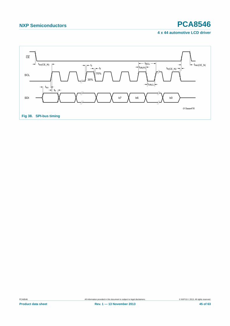
Table 34. Timing characteristics: SPI-busVDD = 1.8 V to 5.5 V; VSS = 0 V; Tamb = 40 C to +95 C. All timing values are valid within the operating supply voltage and temperature range and referenced to VIL and VIH with an input voltage swing of VSS to VDD. Timing waveforms see Figure 38.
Symbol Parameter Conditions VDD < 2.7 V VDD 2.7 V Unit
Min Max Min Max
fclk(SCL) SCL clock frequency - 2 - 5 MHz
tSCL SCL time 500 - 200 - ns
tclk(H) clock HIGH time 200 - 80 - ns
tclk(L) clock LOW time 200 - 80 - ns
tr rise time for SCL signal - 100 - 100 ns
tf fall time for SCL signal - 100 - 100 ns
tsu(CE_N) CE_N set-up time 150 - 80 - ns
th(CE_N) CE_N hold time 0 - 0 - ns
trec(CE_N) CE_N recovery time 100 - 100 - ns
tsu set-up time set-up time for SDI data
10 - 5 - ns
th hold time hold time for SDI data
25 - 10 - ns
PCA8546 All information provided in this document is subject to legal disclaimers. © NXP B.V. 2013. All rights reserved.
Product data sheet Rev. 1 — 13 November 2013 45 of 63
NXP Semiconductors PCA85464 x 44 automotive LCD driver
Fig 38. SPI-bus timing
PCA8546 All information provided in this document is subject to legal disclaimers. © NXP B.V. 2013. All rights reserved.
Product data sheet Rev. 1 — 13 November 2013 46 of 63
NXP Semiconductors PCA85464 x 44 automotive LCD driver
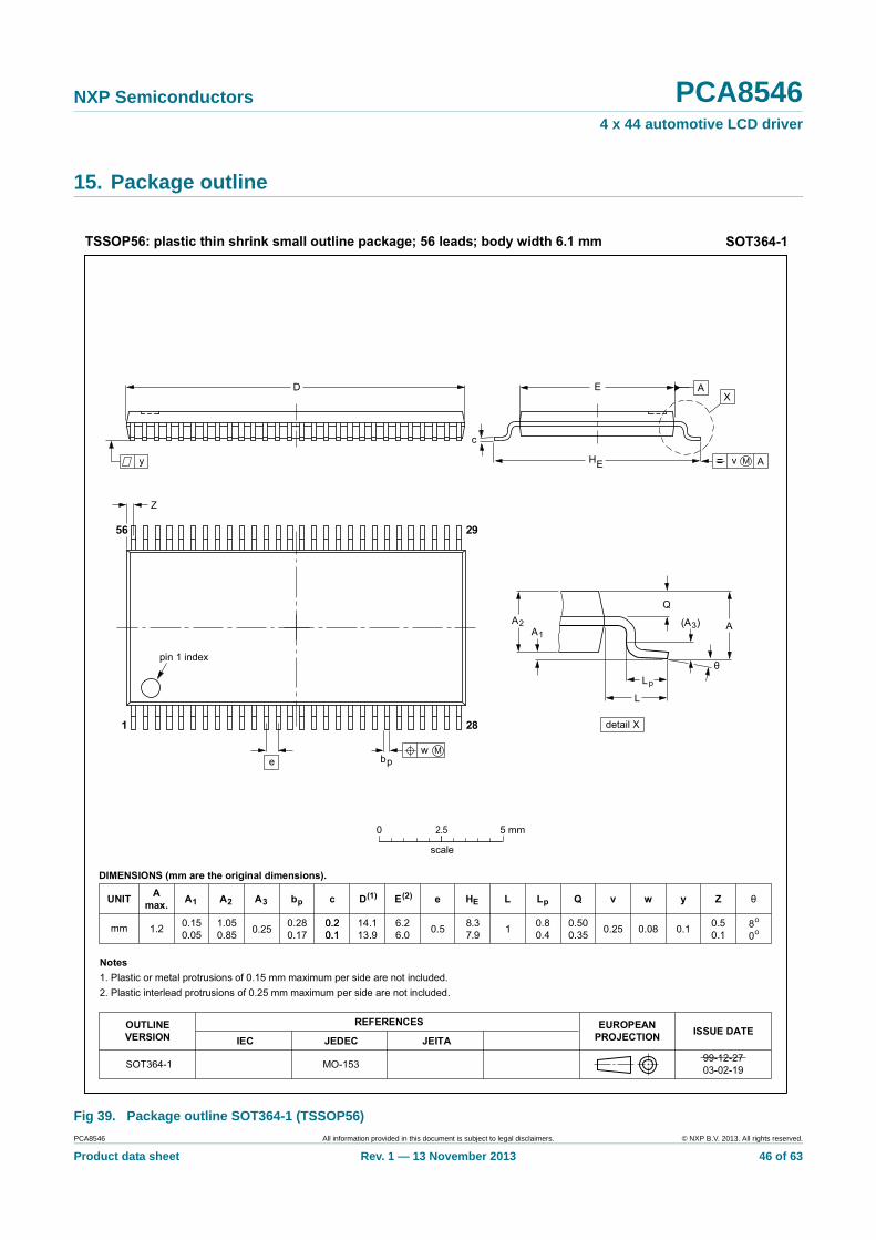
15. Package outline
Fig 39. Package outline SOT364-1 (TSSOP56)
PCA8546 All information provided in this document is subject to legal disclaimers. © NXP B.V. 2013. All rights reserved.
Product data sheet Rev. 1 — 13 November 2013 47 of 63
NXP Semiconductors PCA85464 x 44 automotive LCD driver
16. Handling information
All input and output pins are protected against ElectroStatic Discharge (ESD) under normal handling. When handling Metal-Oxide Semiconductor (MOS) devices ensure that all normal precautions are taken as described in JESD625-A, IEC 61340-5 or equivalent standards.
PCA8546 All information provided in this document is subject to legal disclaimers. © NXP B.V. 2013. All rights reserved.
Product data sheet Rev. 1 — 13 November 2013 48 of 63
NXP Semiconductors PCA85464 x 44 automotive LCD driver
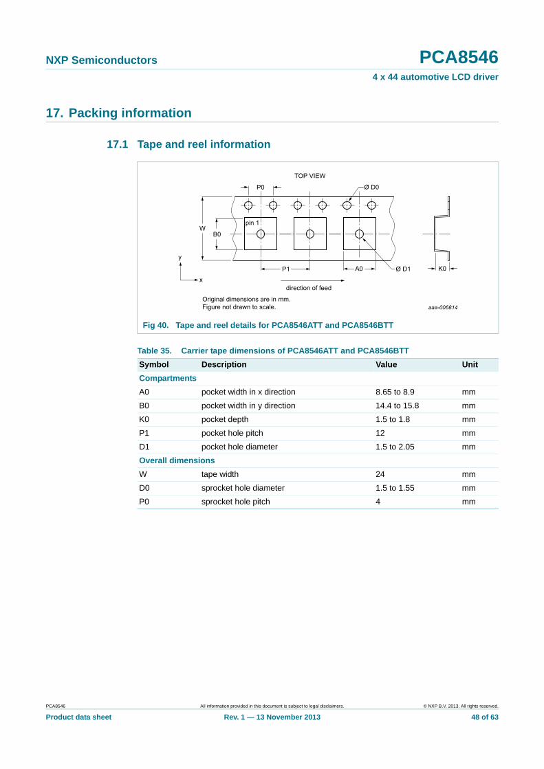
17. Packing information
17.1 Tape and reel information
Fig 40. Tape and reel details for PCA8546ATT and PCA8546BTT
Table 35. Carrier tape dimensions of PCA8546ATT and PCA8546BTT
Symbol Description Value Unit
Compartments
A0 pocket width in x direction 8.65 to 8.9 mm
B0 pocket width in y direction 14.4 to 15.8 mm
K0 pocket depth 1.5 to 1.8 mm
P1 pocket hole pitch 12 mm
D1 pocket hole diameter 1.5 to 2.05 mm
Overall dimensions
W tape width 24 mm
D0 sprocket hole diameter 1.5 to 1.55 mm
P0 sprocket hole pitch 4 mm
PCA8546 All information provided in this document is subject to legal disclaimers. © NXP B.V. 2013. All rights reserved.
Product data sheet Rev. 1 — 13 November 2013 49 of 63
NXP Semiconductors PCA85464 x 44 automotive LCD driver
18. Soldering of SMD packages
This text provides a very brief insight into a complex technology. A more in-depth account of soldering ICs can be found in Application Note AN10365 “Surface mount reflow soldering description”.
18.1 Introduction to soldering
Soldering is one of the most common methods through which packages are attached to Printed Circuit Boards (PCBs), to form electrical circuits. The soldered joint provides both the mechanical and the electrical connection. There is no single soldering method that is ideal for all IC packages. Wave soldering is often preferred when through-hole and Surface Mount Devices (SMDs) are mixed on one printed wiring board; however, it is not suitable for fine pitch SMDs. Reflow soldering is ideal for the small pitches and high densities that come with increased miniaturization.
18.2 Wave and reflow soldering
Wave soldering is a joining technology in which the joints are made by solder coming from a standing wave of liquid solder. The wave soldering process is suitable for the following:
• Through-hole components
• Leaded or leadless SMDs, which are glued to the surface of the printed circuit board
Not all SMDs can be wave soldered. Packages with solder balls, and some leadless packages which have solder lands underneath the body, cannot be wave soldered. Also, leaded SMDs with leads having a pitch smaller than ~0.6 mm cannot be wave soldered, due to an increased probability of bridging.
The reflow soldering process involves applying solder paste to a board, followed by component placement and exposure to a temperature profile. Leaded packages, packages with solder balls, and leadless packages are all reflow solderable.
Key characteristics in both wave and reflow soldering are:
• Board specifications, including the board finish, solder masks and vias
• Package footprints, including solder thieves and orientation
• The moisture sensitivity level of the packages
• Package placement
• Inspection and repair
• Lead-free soldering versus SnPb soldering
18.3 Wave soldering
Key characteristics in wave soldering are:
• Process issues, such as application of adhesive and flux, clinching of leads, board transport, the solder wave parameters, and the time during which components are exposed to the wave
• Solder bath specifications, including temperature and impurities
PCA8546 All information provided in this document is subject to legal disclaimers. © NXP B.V. 2013. All rights reserved.
Product data sheet Rev. 1 — 13 November 2013 50 of 63
NXP Semiconductors PCA85464 x 44 automotive LCD driver
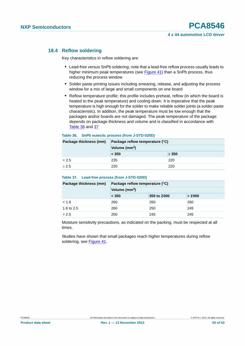
18.4 Reflow soldering
Key characteristics in reflow soldering are:
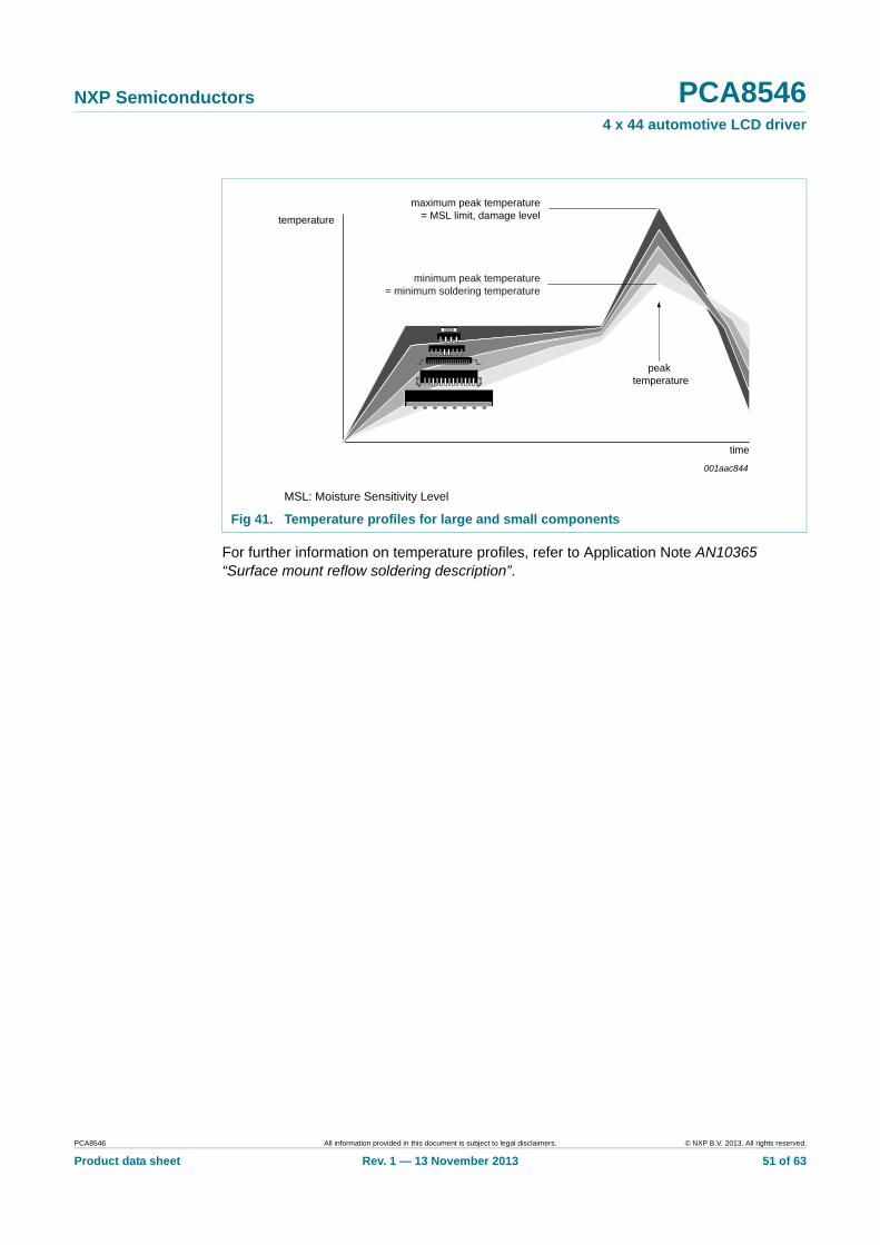
• Lead-free versus SnPb soldering; note that a lead-free reflow process usually leads to higher minimum peak temperatures (see Figure 41) than a SnPb process, thus reducing the process window
• Solder paste printing issues including smearing, release, and adjusting the process window for a mix of large and small components on one board
• Reflow temperature profile; this profile includes preheat, reflow (in which the board is heated to the peak temperature) and cooling down. It is imperative that the peak temperature is high enough for the solder to make reliable solder joints (a solder paste characteristic). In addition, the peak temperature must be low enough that the packages and/or boards are not damaged. The peak temperature of the package depends on package thickness and volume and is classified in accordance with Table 36 and 37
Moisture sensitivity precautions, as indicated on the packing, must be respected at all times.
Studies have shown that small packages reach higher temperatures during reflow soldering, see Figure 41.
Table 36. SnPb eutectic process (from J-STD-020D)
Package thickness (mm) Package reflow temperature (C)
Volume (mm3)
< 350 350
< 2.5 235 220
2.5 220 220
Table 37. Lead-free process (from J-STD-020D)
Package thickness (mm) Package reflow temperature (C)
Volume (mm3)
< 350 350 to 2000 > 2000
< 1.6 260 260 260
1.6 to 2.5 260 250 245
> 2.5 250 245 245
PCA8546 All information provided in this document is subject to legal disclaimers. © NXP B.V. 2013. All rights reserved.
Product data sheet Rev. 1 — 13 November 2013 51 of 63
NXP Semiconductors PCA85464 x 44 automotive LCD driver
For further information on temperature profiles, refer to Application Note AN10365 “Surface mount reflow soldering description”.
MSL: Moisture Sensitivity Level
Fig 41. Temperature profiles for large and small components
001aac844
temperature
time
minimum peak temperature= minimum soldering temperature
maximum peak temperature= MSL limit, damage level
peak temperature
PCA8546 All information provided in this document is subject to legal disclaimers. © NXP B.V. 2013. All rights reserved.
Product data sheet Rev. 1 — 13 November 2013 52 of 63
NXP Semiconductors PCA85464 x 44 automotive LCD driver
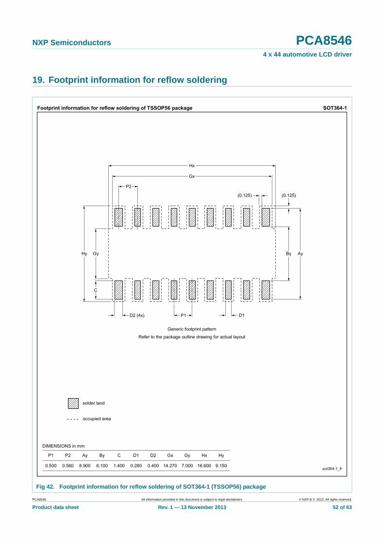
19. Footprint information for reflow soldering
Fig 42. Footprint information for reflow soldering of SOT364-1 (TSSOP56) package
xxxxxxxxxxxxxxxxxxxxx xxxxxxxxxxxxxxxxxxxxxxxxxx xxxxxxx x x x xxxxxxxxxxxxxxxxxxxxxxxxxxxxxx xxxxxxxxxxxxxxxxxxx xx xx xxxxx xxxxxxxxxxxxxxxxxxxxxxxxxxx xxxxxxxxxxxxxxxxxxx xxxxxx xxxxxxxxxxxxxxxxxxxxxxxxxxxxxxxxxxx xxxxxxxxxxxx x x xxxxxxxxxxxxxxxxxxxxx xxxxxxxxxxxxxxxxxxxxxxxxxxxxxx xxxxx xxxxxxxxxxxxxxxxxxxxxxxxxxxxxxxxxxxxxxxxxxxxxxxxxx xxxxxxxx xxxxxxxxxxxxxxxxxxxxxxxxx xxxxxxxxxxxxxxxxxxxx xxx
PC
A854
6A
ll information
provided in this do
cument is sub
ject to legal d
isclaimers.
© N
XP
B.V
. 2013. All rig
hts reserved.
Pro
du
ct data sh
eetR
ev. 1 —
13 No
vemb
er 2013 53 o
f 63
NX
P S
emico
nd
ucto
rsP
CA
85464
x 4
4 auto
mo
tive L
CD
driv
er
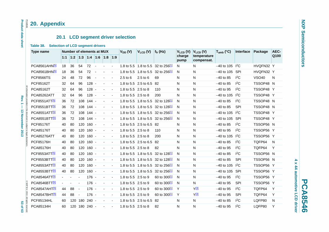
20. Appendix
20.1 LCD segment driver selection
Table 38. Selection of LCD segment drivers
Type name Number of elements at MUX VDD (V) VLCD (V) ffr (Hz) VLCD (V)chargepump
VLCD (V)temperaturecompensat.
Tamb (C) Interface Package AEC-Q1001:1 1:2 1:3 1:4 1:6 1:8 1:9
PCA8561AHN[5] 18 36 54 72 - - - 1.8 to 5.5 1.8 to 5.5 32 to 256[1] N N 40 to 105 I2C HVQFN32 Y
PCA8561BHN[5] 18 36 54 72 - - - 1.8 to 5.5 1.8 to 5.5 32 to 256[1] N N 40 to 105 SPI HVQFN32 Y
PCF8566TS 24 48 72 96 - - - 2.5 to 6 2.5 to 6 69 N N 40 to 85 I2C VSO40 N
PCF85162T 32 64 96 128 - - - 1.8 to 5.5 2.5 to 6.5 82 N N 40 to 85 I2C TSSOP48 N
PCA85162T 32 64 96 128 - - - 1.8 to 5.5 2.5 to 8 110 N N 40 to 95 I2C TSSOP48 Y
PCA85262ATT 32 64 96 128 - - - 1.8 to 5.5 2.5 to 8 200 N N 40 to 105 I2C TSSOP48 Y
PCF8551ATT[5] 36 72 108 144 - - - 1.8 to 5.5 1.8 to 5.5 32 to 128[1] N N 40 to 85 I2C TSSOP48 N
PCF8551BTT[5] 36 72 108 144 - - - 1.8 to 5.5 1.8 to 5.5 32 to 128[1] N N 40 to 85 SPI TSSOP48 N
PCA8551ATT[5] 36 72 108 144 - - - 1.8 to 5.5 1.8 to 5.5 32 to 256[1] N N 40 to 105 I2C TSSOP48 Y
PCA8551BTT[5] 36 72 108 144 - - - 1.8 to 5.5 1.8 to 5.5 32 to 256[1] N N 40 to 105 SPI TSSOP48 Y
PCF85176T 40 80 120 160 - - - 1.8 to 5.5 2.5 to 6.5 82 N N 40 to 85 I2C TSSOP56 N
PCA85176T 40 80 120 160 - - - 1.8 to 5.5 2.5 to 8 110 N N 40 to 95 I2C TSSOP56 Y
PCA85276ATT 40 80 120 160 - - - 1.8 to 5.5 2.5 to 8 200 N N 40 to 105 I2C TSSOP56 Y
PCF85176H 40 80 120 160 - - - 1.8 to 5.5 2.5 to 6.5 82 N N 40 to 85 I2C TQFP64 N
PCA85176H 40 80 120 160 - - - 1.8 to 5.5 2.5 to 8 82 N N 40 to 95 I2C TQFP64 Y
PCF8553ATT[5] 40 80 120 160 - - - 1.8 to 5.5 1.8 to 5.5 32 to 128[1] N N 40 to 85 I2C TSSOP56 N
PCF8553BTT[5] 40 80 120 160 - - - 1.8 to 5.5 1.8 to 5.5 32 to 128[1] N N 40 to 85 SPI TSSOP56 N
PCA8553ATT[5] 40 80 120 160 - - - 1.8 to 5.5 1.8 to 5.5 32 to 256[1] N N 40 to 105 I2C TSSOP56 Y
PCA8553BTT[5] 40 80 120 160 - - - 1.8 to 5.5 1.8 to 5.5 32 to 256[1] N N 40 to 105 SPI TSSOP56 Y
PCA8546ATT[5] - - - 176 - - - 1.8 to 5.5 2.5 to 9 60 to 300[1] N N 40 to 95 I2C TSSOP56 Y
PCA8546BTT[5] - - - 176 - - - 1.8 to 5.5 2.5 to 9 60 to 300[1] N N 40 to 95 SPI TSSOP56 Y
PCA8547AHT[5] 44 88 - 176 - - - 1.8 to 5.5 2.5 to 9 60 to 300[1] Y Y[3] 40 to 95 I2C TQFP64 Y
PCA8547BHT[5] 44 88 - 176 - - - 1.8 to 5.5 2.5 to 9 60 to 300[1] Y Y[3] 40 to 95 SPI TQFP64 Y
PCF85134HL 60 120 180 240 - - - 1.8 to 5.5 2.5 to 6.5 82 N N 40 to 85 I2C LQFP80 N
PCA85134H 60 120 180 240 - - - 1.8 to 5.5 2.5 to 8 82 N N 40 to 95 I2C LQFP80 Y
xxxxxxxxxxxxxxxxxxxxx xxxxxxxxxxxxxxxxxxxxxxxxxx xxxxxxx x x x xxxxxxxxxxxxxxxxxxxxxxxxxxxxxx xxxxxxxxxxxxxxxxxxx xx xx xxxxx xxxxxxxxxxxxxxxxxxxxxxxxxxx xxxxxxxxxxxxxxxxxxx xxxxxx xxxxxxxxxxxxxxxxxxxxxxxxxxxxxxxxxxx xxxxxxxxxxxx x x xxxxxxxxxxxxxxxxxxxxx xxxxxxxxxxxxxxxxxxxxxxxxxxxxxx xxxxx xxxxxxxxxxxxxxxxxxxxxxxxxxxxxxxxxxxxxxxxxxxxxxxxxx xxxxxxxx xxxxxxxxxxxxxxxxxxxxxxxxx xxxxxxxxxxxxxxxxxxxx xxx
PC
A854
6A
ll information
provided in this do
cument is sub
ject to legal d
isclaimers.
© N
XP
B.V
. 2013. All rig
hts reserved.
Pro
du
ct data sh
eetR
ev. 1 —
13 No
vemb
er 2013 54 o
f 63
NX
P S
emico
nd
ucto
rsP
CA
85464
x 4
4 auto
mo
tive L
CD
driv
er
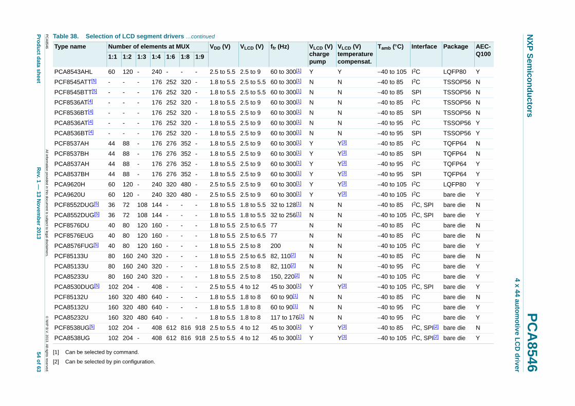
[1] Can be selected by command.
[2] Can be selected by pin configuration.
PCA8543AHL 60 120 - 240 - - - 2.5 to 5.5 2.5 to 9 60 to 300[1] Y Y 40 to 105 I2C LQFP80 Y
PCF8545ATT[5] - - - 176 252 320 - 1.8 to 5.5 2.5 to 5.5 60 to 300[1] N N 40 to 85 I2C TSSOP56 N
PCF8545BTT[5] - - - 176 252 320 - 1.8 to 5.5 2.5 to 5.5 60 to 300[1] N N 40 to 85 SPI TSSOP56 N
PCF8536AT[4] - - - 176 252 320 - 1.8 to 5.5 2.5 to 9 60 to 300[1] N N 40 to 85 I2C TSSOP56 N
PCF8536BT[4] - - - 176 252 320 - 1.8 to 5.5 2.5 to 9 60 to 300[1] N N 40 to 85 SPI TSSOP56 N
PCA8536AT[4] - - - 176 252 320 - 1.8 to 5.5 2.5 to 9 60 to 300[1] N N 40 to 95 I2C TSSOP56 Y
PCA8536BT[4] - - - 176 252 320 - 1.8 to 5.5 2.5 to 9 60 to 300[1] N N 40 to 95 SPI TSSOP56 Y
PCF8537AH 44 88 - 176 276 352 - 1.8 to 5.5 2.5 to 9 60 to 300[1] Y Y[3] 40 to 85 I2C TQFP64 N
PCF8537BH 44 88 - 176 276 352 - 1.8 to 5.5 2.5 to 9 60 to 300[1] Y Y[3] 40 to 85 SPI TQFP64 N
PCA8537AH 44 88 - 176 276 352 - 1.8 to 5.5 2.5 to 9 60 to 300[1] Y Y[3] 40 to 95 I2C TQFP64 Y
PCA8537BH 44 88 - 176 276 352 - 1.8 to 5.5 2.5 to 9 60 to 300[1] Y Y[3] 40 to 95 SPI TQFP64 Y
PCA9620H 60 120 - 240 320 480 - 2.5 to 5.5 2.5 to 9 60 to 300[1] Y Y[3] 40 to 105 I2C LQFP80 Y
PCA9620U 60 120 - 240 320 480 - 2.5 to 5.5 2.5 to 9 60 to 300[1] Y Y[3] 40 to 105 I2C bare die Y
PCF8552DUG[5] 36 72 108 144 - - - 1.8 to 5.5 1.8 to 5.5 32 to 128[1] N N 40 to 85 I2C, SPI bare die N
PCA8552DUG[5] 36 72 108 144 - - - 1.8 to 5.5 1.8 to 5.5 32 to 256[1] N N 40 to 105 I2C, SPI bare die Y
PCF8576DU 40 80 120 160 - - - 1.8 to 5.5 2.5 to 6.5 77 N N 40 to 85 I2C bare die N
PCF8576EUG 40 80 120 160 - - - 1.8 to 5.5 2.5 to 6.5 77 N N 40 to 85 I2C bare die N
PCA8576FUG[5] 40 80 120 160 - - - 1.8 to 5.5 2.5 to 8 200 N N 40 to 105 I2C bare die Y
PCF85133U 80 160 240 320 - - - 1.8 to 5.5 2.5 to 6.5 82, 110[2] N N 40 to 85 I2C bare die N
PCA85133U 80 160 240 320 - - - 1.8 to 5.5 2.5 to 8 82, 110[2] N N 40 to 95 I2C bare die Y
PCA85233U 80 160 240 320 - - - 1.8 to 5.5 2.5 to 8 150, 220[2] N N 40 to 105 I2C bare die Y
PCA8530DUG[5] 102 204 - 408 - - - 2.5 to 5.5 4 to 12 45 to 300[1] Y Y[3] 40 to 105 I2C, SPI bare die Y
PCF85132U 160 320 480 640 - - - 1.8 to 5.5 1.8 to 8 60 to 90[1] N N 40 to 85 I2C bare die N
PCA85132U 160 320 480 640 - - - 1.8 to 5.5 1.8 to 8 60 to 90[1] N N 40 to 95 I2C bare die Y
PCA85232U 160 320 480 640 - - - 1.8 to 5.5 1.8 to 8 117 to 176[1] N N 40 to 95 I2C bare die Y
PCF8538UG[5] 102 204 - 408 612 816 918 2.5 to 5.5 4 to 12 45 to 300[1] Y Y[3] 40 to 85 I2C, SPI[2] bare die N
PCA8538UG 102 204 - 408 612 816 918 2.5 to 5.5 4 to 12 45 to 300[1] Y Y[3] 40 to 105 I2C, SPI[2] bare die Y
Table 38. Selection of LCD segment drivers …continued
Type name Number of elements at MUX VDD (V) VLCD (V) ffr (Hz) VLCD (V)chargepump
VLCD (V)temperaturecompensat.
Tamb (C) Interface Package AEC-Q1001:1 1:2 1:3 1:4 1:6 1:8 1:9
xxxxxxxxxxxxxxxxxxxxx xxxxxxxxxxxxxxxxxxxxxxxxxx xxxxxxx x x x xxxxxxxxxxxxxxxxxxxxxxxxxxxxxx xxxxxxxxxxxxxxxxxxx xx xx xxxxx xxxxxxxxxxxxxxxxxxxxxxxxxxx xxxxxxxxxxxxxxxxxxx xxxxxx xxxxxxxxxxxxxxxxxxxxxxxxxxxxxxxxxxx xxxxxxxxxxxx x x xxxxxxxxxxxxxxxxxxxxx xxxxxxxxxxxxxxxxxxxxxxxxxxxxxx xxxxx xxxxxxxxxxxxxxxxxxxxxxxxxxxxxxxxxxxxxxxxxxxxxxxxxx xxxxxxxx xxxxxxxxxxxxxxxxxxxxxxxxx xxxxxxxxxxxxxxxxxxxx xxx
PC
A854
6A
ll information
provided in this do
cument is sub
ject to legal d
isclaimers.
© N
XP
B.V
. 2013. All rig
hts reserved.
Pro
du
ct data sh
eetR
ev. 1 —
13 No
vemb
er 2013 55 o
f 63
NX
P S
emico
nd
ucto
rsP
CA
85464
x 4
4 auto
mo
tive L
CD
driv
er
[3] Extra feature: Temperature sensor.
[4] Extra feature: 6 PWM channels.
[5] In development.
PCA8546 All information provided in this document is subject to legal disclaimers. © NXP B.V. 2013. All rights reserved.
Product data sheet Rev. 1 — 13 November 2013 56 of 63
NXP Semiconductors PCA85464 x 44 automotive LCD driver
21. Abbreviations
Table 39. Abbreviations
Acronym Description
CDM Charged-Device Model
CMOS Complementary Metal-Oxide Semiconductor
DC Direct Current
EMC ElectroMagnetic Compatibility
EPROM Erasable Programmable Read-Only Memory
ESD ElectroStatic Discharge
HBM Human Body Model
I2C Inter-Integrated Circuit bus
IC Integrated Circuit
LCD Liquid Crystal Display
LSB Least Significant Bit
MSB Most Significant Bit
MSL Moisture Sensitivity Level
MUX Multiplexer
OTP One Time Programmable
PCB Printed-Circuit Board
POR Power-On Reset
RC Resistance-Capacitance
RAM Random Access Memory
RGB Red Green Blue
RMS Root Mean Square
SCL Serial CLock line
SDA Serial DAta line
SPI Serial Peripheral Interface
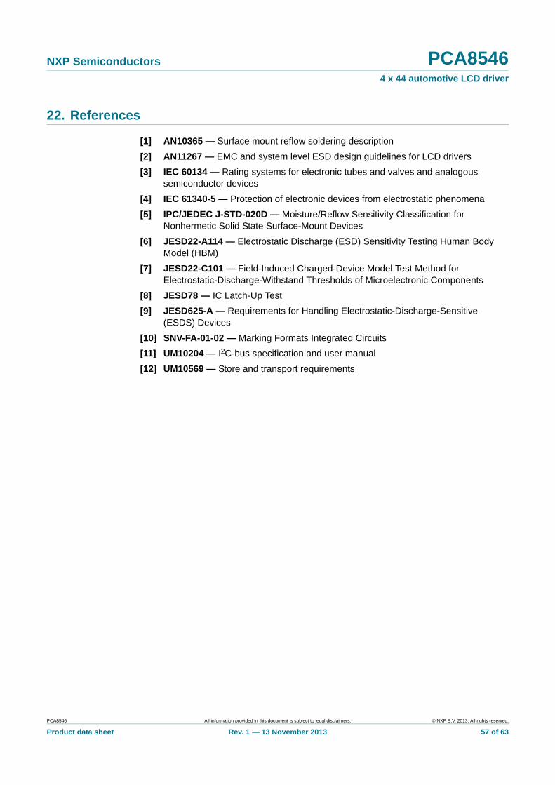
PCA8546 All information provided in this document is subject to legal disclaimers. © NXP B.V. 2013. All rights reserved.
Product data sheet Rev. 1 — 13 November 2013 57 of 63
NXP Semiconductors PCA85464 x 44 automotive LCD driver
22. References
[1] AN10365 — Surface mount reflow soldering description
[2] AN11267 — EMC and system level ESD design guidelines for LCD drivers
[3] IEC 60134 — Rating systems for electronic tubes and valves and analogous semiconductor devices
[4] IEC 61340-5 — Protection of electronic devices from electrostatic phenomena
[5] IPC/JEDEC J-STD-020D — Moisture/Reflow Sensitivity Classification for Nonhermetic Solid State Surface-Mount Devices
[6] JESD22-A114 — Electrostatic Discharge (ESD) Sensitivity Testing Human Body Model (HBM)
[7] JESD22-C101 — Field-Induced Charged-Device Model Test Method for Electrostatic-Discharge-Withstand Thresholds of Microelectronic Components
[8] JESD78 — IC Latch-Up Test
[9] JESD625-A — Requirements for Handling Electrostatic-Discharge-Sensitive (ESDS) Devices
[10] SNV-FA-01-02 — Marking Formats Integrated Circuits
[11] UM10204 — I2C-bus specification and user manual
[12] UM10569 — Store and transport requirements
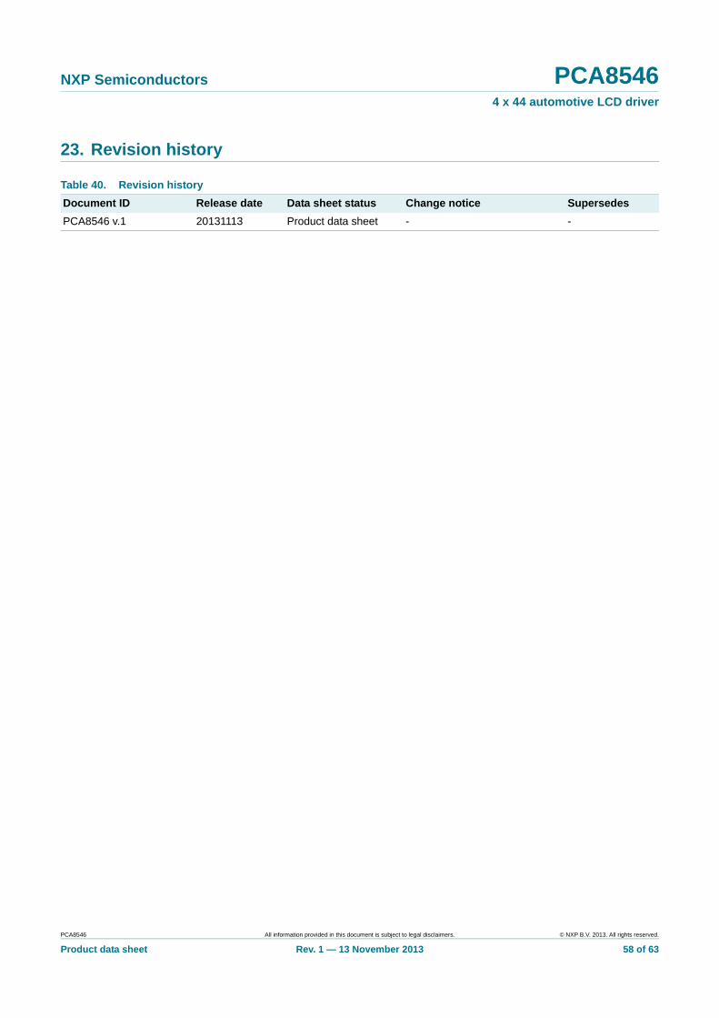
PCA8546 All information provided in this document is subject to legal disclaimers. © NXP B.V. 2013. All rights reserved.
Product data sheet Rev. 1 — 13 November 2013 58 of 63
NXP Semiconductors PCA85464 x 44 automotive LCD driver
23. Revision history
Table 40. Revision history
Document ID Release date Data sheet status Change notice Supersedes
PCA8546 v.1 20131113 Product data sheet - -
PCA8546 All information provided in this document is subject to legal disclaimers. © NXP B.V. 2013. All rights reserved.
Product data sheet Rev. 1 — 13 November 2013 59 of 63
NXP Semiconductors PCA85464 x 44 automotive LCD driver
24. Legal information
24.1 Data sheet status
[1] Please consult the most recently issued document before initiating or completing a design.
[2] The term ‘short data sheet’ is explained in section “Definitions”.
[3] The product status of device(s) described in this document may have changed since this document was published and may differ in case of multiple devices. The latest product status information is available on the Internet at URL http://www.nxp.com.
24.2 Definitions
Draft — The document is a draft version only. The content is still under internal review and subject to formal approval, which may result in modifications or additions. NXP Semiconductors does not give any representations or warranties as to the accuracy or completeness of information included herein and shall have no liability for the consequences of use of such information.
Short data sheet — A short data sheet is an extract from a full data sheet with the same product type number(s) and title. A short data sheet is intended for quick reference only and should not be relied upon to contain detailed and full information. For detailed and full information see the relevant full data sheet, which is available on request via the local NXP Semiconductors sales office. In case of any inconsistency or conflict with the short data sheet, the full data sheet shall prevail.
Product specification — The information and data provided in a Product data sheet shall define the specification of the product as agreed between NXP Semiconductors and its customer, unless NXP Semiconductors and customer have explicitly agreed otherwise in writing. In no event however, shall an agreement be valid in which the NXP Semiconductors product is deemed to offer functions and qualities beyond those described in the Product data sheet.
24.3 Disclaimers
Limited warranty and liability — Information in this document is believed to be accurate and reliable. However, NXP Semiconductors does not give any representations or warranties, expressed or implied, as to the accuracy or completeness of such information and shall have no liability for the consequences of use of such information. NXP Semiconductors takes no responsibility for the content in this document if provided by an information source outside of NXP Semiconductors.
In no event shall NXP Semiconductors be liable for any indirect, incidental, punitive, special or consequential damages (including - without limitation - lost profits, lost savings, business interruption, costs related to the removal or replacement of any products or rework charges) whether or not such damages are based on tort (including negligence), warranty, breach of contract or any other legal theory.
Notwithstanding any damages that customer might incur for any reason whatsoever, NXP Semiconductors’ aggregate and cumulative liability towards customer for the products described herein shall be limited in accordance with the Terms and conditions of commercial sale of NXP Semiconductors.
Right to make changes — NXP Semiconductors reserves the right to make changes to information published in this document, including without limitation specifications and product descriptions, at any time and without notice. This document supersedes and replaces all information supplied prior to the publication hereof.
Suitability for use in automotive applications — This NXP Semiconductors product has been qualified for use in automotive applications. Unless otherwise agreed in writing, the product is not designed, authorized or warranted to be suitable for use in life support, life-critical or safety-critical systems or equipment, nor in applications where failure or malfunction of an NXP Semiconductors product can reasonably be expected to result in personal injury, death or severe property or environmental damage. NXP Semiconductors and its suppliers accept no liability for inclusion and/or use of NXP Semiconductors products in such equipment or applications and therefore such inclusion and/or use is at the customer's own risk.
Applications — Applications that are described herein for any of these products are for illustrative purposes only. NXP Semiconductors makes no representation or warranty that such applications will be suitable for the specified use without further testing or modification.
Customers are responsible for the design and operation of their applications and products using NXP Semiconductors products, and NXP Semiconductors accepts no liability for any assistance with applications or customer product design. It is customer’s sole responsibility to determine whether the NXP Semiconductors product is suitable and fit for the customer’s applications and products planned, as well as for the planned application and use of customer’s third party customer(s). Customers should provide appropriate design and operating safeguards to minimize the risks associated with their applications and products.
NXP Semiconductors does not accept any liability related to any default, damage, costs or problem which is based on any weakness or default in the customer’s applications or products, or the application or use by customer’s third party customer(s). Customer is responsible for doing all necessary testing for the customer’s applications and products using NXP Semiconductors products in order to avoid a default of the applications and the products or of the application or use by customer’s third party customer(s). NXP does not accept any liability in this respect.
Limiting values — Stress above one or more limiting values (as defined in the Absolute Maximum Ratings System of IEC 60134) will cause permanent damage to the device. Limiting values are stress ratings only and (proper) operation of the device at these or any other conditions above those given in the Recommended operating conditions section (if present) or the Characteristics sections of this document is not warranted. Constant or repeated exposure to limiting values will permanently and irreversibly affect the quality and reliability of the device.
Terms and conditions of commercial sale — NXP Semiconductors products are sold subject to the general terms and conditions of commercial sale, as published at http://www.nxp.com/profile/terms, unless otherwise agreed in a valid written individual agreement. In case an individual agreement is concluded only the terms and conditions of the respective agreement shall apply. NXP Semiconductors hereby expressly objects to applying the customer’s general terms and conditions with regard to the purchase of NXP Semiconductors products by customer.
Document status[1][2] Product status[3] Definition
Objective [short] data sheet Development This document contains data from the objective specification for product development.
Preliminary [short] data sheet Qualification This document contains data from the preliminary specification.
Product [short] data sheet Production This document contains the product specification.
PCA8546 All information provided in this document is subject to legal disclaimers. © NXP B.V. 2013. All rights reserved.
Product data sheet Rev. 1 — 13 November 2013 60 of 63
NXP Semiconductors PCA85464 x 44 automotive LCD driver
No offer to sell or license — Nothing in this document may be interpreted or construed as an offer to sell products that is open for acceptance or the grant, conveyance or implication of any license under any copyrights, patents or other industrial or intellectual property rights.
Export control — This document as well as the item(s) described herein may be subject to export control regulations. Export might require a prior authorization from competent authorities.
Translations — A non-English (translated) version of a document is for reference only. The English version shall prevail in case of any discrepancy between the translated and English versions.
24.4 TrademarksNotice: All referenced brands, product names, service names and trademarks are the property of their respective owners.
I2C-bus — logo is a trademark of NXP B.V.
25. Contact information
For more information, please visit: http://www.nxp.com
For sales office addresses, please send an email to: [email protected]
PCA8546 All information provided in this document is subject to legal disclaimers. © NXP B.V. 2013. All rights reserved.
Product data sheet Rev. 1 — 13 November 2013 61 of 63
NXP Semiconductors PCA85464 x 44 automotive LCD driver
26. Tables
Table 1. Ordering information . . . . . . . . . . . . . . . . . . . . .2Table 2. Ordering options . . . . . . . . . . . . . . . . . . . . . . . . .2Table 3. Marking codes . . . . . . . . . . . . . . . . . . . . . . . . . .2Table 4. Pin description of PCA8546ATT and
PCA8546BTT . . . . . . . . . . . . . . . . . . . . . . . . . .6Table 5. Commands of PCA8546 . . . . . . . . . . . . . . . . . .7Table 6. Initialize - initialize command bit description . . .7Table 7. OTP-refresh - OTP-refresh command bit
description . . . . . . . . . . . . . . . . . . . . . . . . . . . . .8Table 8. Mode-settings - mode settings command
bit description . . . . . . . . . . . . . . . . . . . . . . . . . .8Table 9. Effect of the power-down bit (PD). . . . . . . . . . .10Table 10. Oscillator-control - oscillator control command
bit description . . . . . . . . . . . . . . . . . . . . . . . . . 11Table 11. Valid combinations of bits OSC, EFR,
and COE. . . . . . . . . . . . . . . . . . . . . . . . . . . . . .12Table 12. Typical use of bits OSC, EFR, and COE . . . . .12Table 13. OSCCLK pin state depending on configuration 13Table 14. LCD frame frequencies. . . . . . . . . . . . . . . . . . .13Table 15. Set-bias-mode - set bias mode command
bit description . . . . . . . . . . . . . . . . . . . . . . . . .14Table 16. Frame-frequency - frame frequency and output
clock frequency command bit description . . . .14Table 17. Frame frequency prescaler values for 230 kHz
clock operation . . . . . . . . . . . . . . . . . . . . . . . .14Table 18. Load-data-pointer - load data pointer
command bit description. . . . . . . . . . . . . . . . . .15Table 19. Write-RAM-data - write RAM data command
bit description . . . . . . . . . . . . . . . . . . . . . . . . .16Table 20. Starting conditions . . . . . . . . . . . . . . . . . . . . . .17Table 21. Display configuration . . . . . . . . . . . . . . . . . . . .20Table 22. Preferred LCD drive modes: summary
of characteristics. . . . . . . . . . . . . . . . . . . . . . . .22Table 23. Control byte description . . . . . . . . . . . . . . . . . .29Table 24. I2C slave address byte . . . . . . . . . . . . . . . . . . .32Table 25. R/W-bit description . . . . . . . . . . . . . . . . . . . . . .32Table 26. Status read out value . . . . . . . . . . . . . . . . . . . .33Table 27. Modified status read out value . . . . . . . . . . . . .34Table 28. Serial interface . . . . . . . . . . . . . . . . . . . . . . . . .34Table 29. Subaddress byte definition . . . . . . . . . . . . . . . .34Table 30. Limiting values . . . . . . . . . . . . . . . . . . . . . . . . .37Table 31. Static characteristics . . . . . . . . . . . . . . . . . . . .38Table 32. Dynamic characteristics . . . . . . . . . . . . . . . . . .42Table 33. Timing characteristics: I2C-bus . . . . . . . . . . . .43Table 34. Timing characteristics: SPI-bus . . . . . . . . . . . .44Table 35. Carrier tape dimensions of PCA8546ATT
and PCA8546BTT . . . . . . . . . . . . . . . . . . . . .48Table 36. SnPb eutectic process (from J-STD-020D) . . .50Table 37. Lead-free process (from J-STD-020D) . . . . . .50Table 38. Selection of LCD segment drivers . . . . . . . . . .53Table 39. Abbreviations . . . . . . . . . . . . . . . . . . . . . . . . . .56Table 40. Revision history . . . . . . . . . . . . . . . . . . . . . . . .58
PCA8546 All information provided in this document is subject to legal disclaimers. © NXP B.V. 2013. All rights reserved.
Product data sheet Rev. 1 — 13 November 2013 62 of 63
NXP Semiconductors PCA85464 x 44 automotive LCD driver
27. Figures
Fig 1. Block diagram of PCA8546A . . . . . . . . . . . . . . . . .3Fig 2. Block diagram of PCA8546B . . . . . . . . . . . . . . . . .4Fig 3. Pin configuration for TSSOP56 (PCA8546ATT) . .5Fig 4. Pin configuration for TSSOP56 (PCA8546BTT) . .5Fig 5. Effect of backplane swapping . . . . . . . . . . . . . . . .9Fig 6. Recommended power-down sequence . . . . . . . .10Fig 7. Oscillator selection. . . . . . . . . . . . . . . . . . . . . . . .12Fig 8. Recommended start-up sequence when
using an external clock signal . . . . . . . . . . . . . . .18Fig 9. Recommended start-up sequence when
using the internal oscillator . . . . . . . . . . . . . . . . .19Fig 10. Example of displays suitable for PCA8546 . . . . .20Fig 11. Typical system configuration for the I2C-bus . . . .20Fig 12. Typical system configuration for the SPI-bus. . . .21Fig 13. Electro-optical characteristic: relative
transmission curve of the liquid . . . . . . . . . . . . . .23Fig 14. Waveforms for the 1:4 multiplex drive mode
with 1⁄3 bias and line inversion . . . . . . . . . . . . . . .24Fig 15. Waveforms for 1:4 multiplex drive mode
with 1⁄3 bias and frame inversion . . . . . . . . . . . . .25Fig 16. Display RAM bitmap . . . . . . . . . . . . . . . . . . . . . .26Fig 17. Display RAM filling order in 1:4 multiplex
drive mode . . . . . . . . . . . . . . . . . . . . . . . . . . . . . .27Fig 18. Boundary condition in 1:4 multiplex drive mode .28Fig 19. Control byte format . . . . . . . . . . . . . . . . . . . . . . .29Fig 20. Bit transfer . . . . . . . . . . . . . . . . . . . . . . . . . . . . . .30Fig 21. Definition of START and STOP conditions. . . . . .30Fig 22. System configuration . . . . . . . . . . . . . . . . . . . . . .30Fig 23. Acknowledgement on the I2C-bus . . . . . . . . . . . .31Fig 24. I2C-bus protocol write mode . . . . . . . . . . . . . . . .33Fig 25. I2C-bus protocol read mode. . . . . . . . . . . . . . . . .33Fig 26. Data transfer overview. . . . . . . . . . . . . . . . . . . . .34Fig 27. SPI-bus write example. . . . . . . . . . . . . . . . . . . . .35Fig 28. SPI-bus example . . . . . . . . . . . . . . . . . . . . . . . . .35Fig 29. Device protection diagram for PCA8546A . . . . . .36Fig 30. Device protection diagram for PCA8546B . . . . . .36Fig 31. Typical IDD with respect to temperature . . . . . . . .40Fig 32. Typical IDD(LCD) in power-down mode
with respect to temperature . . . . . . . . . . . . . . . . .40Fig 33. Typical IDD(LCD) when display is active
with respect to temperature . . . . . . . . . . . . . . . . .41Fig 34. Typical clock frequency with respect to VDD
and temperature . . . . . . . . . . . . . . . . . . . . . . . . .42Fig 35. Driver timing waveforms . . . . . . . . . . . . . . . . . . .42Fig 36. RESET timing . . . . . . . . . . . . . . . . . . . . . . . . . . .43Fig 37. I2C-bus timing waveforms . . . . . . . . . . . . . . . . . .44Fig 38. SPI-bus timing . . . . . . . . . . . . . . . . . . . . . . . . . . .45Fig 39. Package outline SOT364-1 (TSSOP56) . . . . . . .46Fig 40. Tape and reel details for PCA8546ATT
and PCA8546BTT . . . . . . . . . . . . . . . . . . . . . . . .48Fig 41. Temperature profiles for large and small
components . . . . . . . . . . . . . . . . . . . . . . . . . . . . .51Fig 42. Footprint information for reflow soldering of
SOT364-1 (TSSOP56) package . . . . . . . . . . . . .52
NXP Semiconductors PCA85464 x 44 automotive LCD driver
© NXP B.V. 2013. All rights reserved.
For more information, please visit: http://www.nxp.comFor sales office addresses, please send an email to: [email protected]
Date of release: 13 November 2013
Document identifier: PCA8546
Please be aware that important notices concerning this document and the product(s)described herein, have been included in section ‘Legal information’.
28. Contents
1 General description . . . . . . . . . . . . . . . . . . . . . . 1
2 Features and benefits . . . . . . . . . . . . . . . . . . . . 1
3 Applications . . . . . . . . . . . . . . . . . . . . . . . . . . . . 1
4 Ordering information. . . . . . . . . . . . . . . . . . . . . 24.1 Ordering options . . . . . . . . . . . . . . . . . . . . . . . . 2
5 Marking . . . . . . . . . . . . . . . . . . . . . . . . . . . . . . . . 2
6 Block diagram . . . . . . . . . . . . . . . . . . . . . . . . . . 3
7 Pinning information. . . . . . . . . . . . . . . . . . . . . . 57.1 Pinning . . . . . . . . . . . . . . . . . . . . . . . . . . . . . . . 57.2 Pin description . . . . . . . . . . . . . . . . . . . . . . . . . 6
8 Functional description . . . . . . . . . . . . . . . . . . . 78.1 Commands of PCA8546. . . . . . . . . . . . . . . . . . 78.1.1 Command: initialize . . . . . . . . . . . . . . . . . . . . . 78.1.2 Command: OTP-refresh . . . . . . . . . . . . . . . . . . 78.1.3 Command: mode-settings . . . . . . . . . . . . . . . . 88.1.3.1 Backplane swapping. . . . . . . . . . . . . . . . . . . . . 88.1.3.2 Line inversion (driving scheme A) and frame
inversion (driving scheme B) . . . . . . . . . . . . . . 98.1.3.3 Power-down mode . . . . . . . . . . . . . . . . . . . . . . 98.1.3.4 Display enable . . . . . . . . . . . . . . . . . . . . . . . . 118.1.4 Command: oscillator-control . . . . . . . . . . . . . 118.1.4.1 Oscillator. . . . . . . . . . . . . . . . . . . . . . . . . . . . . 128.1.4.2 Timing and frame frequency . . . . . . . . . . . . . . 138.1.5 Command: set-bias-mode . . . . . . . . . . . . . . . 138.1.6 Command: frame-frequency. . . . . . . . . . . . . . 148.1.7 Command: load-data-pointer . . . . . . . . . . . . . 158.1.8 Command: write-RAM-data . . . . . . . . . . . . . . 158.2 Start-up and shut-down. . . . . . . . . . . . . . . . . . 178.2.1 Reset and Power-On Reset (POR). . . . . . . . . 178.2.2 RESET pin function . . . . . . . . . . . . . . . . . . . . 178.2.3 Recommended start-up sequences . . . . . . . . 178.3 Possible display configurations . . . . . . . . . . . 208.4 LCD voltage selector . . . . . . . . . . . . . . . . . . . 228.4.1 Electro-optical performance . . . . . . . . . . . . . . 238.5 LCD drive mode waveforms . . . . . . . . . . . . . . 248.5.1 1⁄3 bias and line inversion . . . . . . . . . . . . . . . . 248.5.2 1⁄3 bias and frame inversion . . . . . . . . . . . . . . 258.6 Display register . . . . . . . . . . . . . . . . . . . . . . . . 258.7 Backplane outputs . . . . . . . . . . . . . . . . . . . . . 268.8 Segment outputs. . . . . . . . . . . . . . . . . . . . . . . 268.9 Display RAM. . . . . . . . . . . . . . . . . . . . . . . . . . 268.9.1 Data pointer . . . . . . . . . . . . . . . . . . . . . . . . . . 278.9.2 RAM filling . . . . . . . . . . . . . . . . . . . . . . . . . . . 27
9 Bus interfaces . . . . . . . . . . . . . . . . . . . . . . . . . 299.1 Control byte and register selection . . . . . . . . . 299.2 I2C-bus interface. . . . . . . . . . . . . . . . . . . . . . . 29
9.2.1 Bit transfer . . . . . . . . . . . . . . . . . . . . . . . . . . . 309.2.2 START and STOP conditions. . . . . . . . . . . . . 309.2.3 System configuration . . . . . . . . . . . . . . . . . . . 309.2.4 Acknowledge . . . . . . . . . . . . . . . . . . . . . . . . . 319.2.5 I2C-bus controller . . . . . . . . . . . . . . . . . . . . . . 319.2.6 Input filters . . . . . . . . . . . . . . . . . . . . . . . . . . . 319.2.7 I2C-bus slave address . . . . . . . . . . . . . . . . . . 319.2.8 I2C-bus protocol . . . . . . . . . . . . . . . . . . . . . . . 329.2.8.1 Status read out. . . . . . . . . . . . . . . . . . . . . . . . 339.3 SPI-bus interface . . . . . . . . . . . . . . . . . . . . . . 349.3.1 Data transmission . . . . . . . . . . . . . . . . . . . . . 34
10 Internal circuitry . . . . . . . . . . . . . . . . . . . . . . . 36
11 Safety notes. . . . . . . . . . . . . . . . . . . . . . . . . . . 36
12 Limiting values . . . . . . . . . . . . . . . . . . . . . . . . 37
13 Static characteristics . . . . . . . . . . . . . . . . . . . 38
14 Dynamic characteristics. . . . . . . . . . . . . . . . . 42
15 Package outline. . . . . . . . . . . . . . . . . . . . . . . . 46
16 Handling information . . . . . . . . . . . . . . . . . . . 47
17 Packing information . . . . . . . . . . . . . . . . . . . . 4817.1 Tape and reel information . . . . . . . . . . . . . . . 48
18 Soldering of SMD packages. . . . . . . . . . . . . . 4918.1 Introduction to soldering. . . . . . . . . . . . . . . . . 4918.2 Wave and reflow soldering. . . . . . . . . . . . . . . 4918.3 Wave soldering . . . . . . . . . . . . . . . . . . . . . . . 4918.4 Reflow soldering . . . . . . . . . . . . . . . . . . . . . . 50
19 Footprint information for reflow soldering . . 51
20 Appendix . . . . . . . . . . . . . . . . . . . . . . . . . . . . . 5320.1 LCD segment driver selection . . . . . . . . . . . . 53
21 Abbreviations . . . . . . . . . . . . . . . . . . . . . . . . . 56
22 References. . . . . . . . . . . . . . . . . . . . . . . . . . . . 57
23 Revision history . . . . . . . . . . . . . . . . . . . . . . . 58
24 Legal information . . . . . . . . . . . . . . . . . . . . . . 5924.1 Data sheet status . . . . . . . . . . . . . . . . . . . . . . 5924.2 Definitions . . . . . . . . . . . . . . . . . . . . . . . . . . . 5924.3 Disclaimers . . . . . . . . . . . . . . . . . . . . . . . . . . 5924.4 Trademarks . . . . . . . . . . . . . . . . . . . . . . . . . . 60
25 Contact information . . . . . . . . . . . . . . . . . . . . 60
26 Tables . . . . . . . . . . . . . . . . . . . . . . . . . . . . . . . . 61
27 Figures . . . . . . . . . . . . . . . . . . . . . . . . . . . . . . . 62
28 Contents. . . . . . . . . . . . . . . . . . . . . . . . . . . . . . 63
Mouser Electronics
Authorized Distributor
Click to View Pricing, Inventory, Delivery & Lifecycle Information: NXP:
PCA8546ATT/AJ PCA8546BTT/AJ