
Pb CALCE Research on Risk Assessment, Mitigation, and ...Max Range (˚C) 15 75* 75* 75* 15 15 15...
34
University of Maryland Copyright © 2005 CALCE EPSC Electronic Products and Systems Center 1 Electronic Products and Systems Center University of Maryland College Park, MD 20742 (301) 405-5323 http://www.calce.umd.edu ISO 9001 Certified, 1999 Formed 1987 CALCE CALCE Research on Risk Assessment, Mitigation, Research on Risk Assessment, Mitigation, and Management for and Management for Pb Pb - - free Electronics free Electronics Michael Osterman [email protected] Pb
Transcript of Pb CALCE Research on Risk Assessment, Mitigation, and ...Max Range (˚C) 15 75* 75* 75* 15 15 15...
University of MarylandCopyright © 2005 CALCE EPSC
Electronic Products and Systems Center 1
Electronic Products and Systems CenterUniversity of MarylandCollege Park, MD 20742
(301) 405-5323http://www.calce.umd.edu
ISO 9001 Certified, 1999Formed 1987
CALCE CALCE Research on Risk Assessment, Mitigation, Research on Risk Assessment, Mitigation,
and Management for and Management for PbPb--free Electronicsfree Electronics
Michael [email protected]
Pb

University of MarylandCopyright © 2005 CALCE EPSC
Electronic Products and Systems Center 2
What is CALCE?CALCE EPSC Mission:
CALCE Electronic Products and Systems Center (founded 1987) is dedicated to providing a knowledge and resource base to support the development and sustainment of competitive electronic components, products and systems.
Areas of • Physics of Failure • Design of Reliability• Accelerated Qualification• Supply-chain Management• Prognostics• Obsolescence
CALCECALCEElectronic Productsand Systems Center
~$5M/Year
CALCEElectronic Products
& Systems Center (EPSC)~$5 million/yr Risk Mgmt in
Avionics Systems
• Manufacturing for sustainment (USAF ManTech Program)
• IEC and avionics workinggroup collaboration
LabServices
• Small jobs• Fee-for-service• Proprietary work• Use of CALCE Tools &
Methods• Turnkey capabilities• “Fire-fighting”
MEMSTechnology
• Combined RF MEMS and Si/Ge Hetrojunction Bipolar Transistors (HBTs)
• MEMS chip-to-chip bonding reliability
Research Contracts
• Larger programs• Some past programs:• Power Electronics (Navy)• Embedded Passives (NIST)• Risk Management (USAF)• Life Assessment (NASA)• MEMS (NASA,NSWC)
• Risk assessment, mitigationand management of electronic products and systems
CALCE Electronic Products
and Systems Consortium
CALCEConsortium
• 40-45 companies• Pre-competitive research• Risk assessment,
management, and mitigation for electronics
CALCE EPSC Personnel:
~26 Faculty and Research StaffEEs, MEs, MatSci, Physics4 Software Developers
~19 M.S. students~66 Ph.D. students http://www.calce.umd.edu

University of MarylandCopyright © 2005 CALCE EPSC
Electronic Products and Systems Center 3
Pb-Free Movement- Overview of European Union Legislation -
WEEE (Waste of Electrical and Electronic Equipment ) – Requires manufacturers to reduce the disposal waste of electronic products
by reuse, recycling and other forms of recovery– Member states can set more severe requirements than those in the
directive, based on Article 175 of the treaty.
RoHS (Restriction of Use of Hazardous Substances) – Bans the use of Pb, Hg, Cd, Cr, Polybrominated biphenyls (PBBs), and
Polybrominated diphenyl ethers (PBDEs) by July 1, 2006– This ‘Single Market’ directive will be implemented by creating
harmonized standards for the EU’s international market. Namely, member states cannot pass more restrictive national laws.
Member states of EU were required to put national laws into place by August 13, 2004.

University of MarylandCopyright © 2005 CALCE EPSC
Electronic Products and Systems Center 4
Current Pb-free Exemptions in RoHS1. Defense related electronics2. Lead in electronic ceramic parts3. Lead in glass cathode ray tubes, electronics components, and
fluorescence tubes 4. Lead in solders for servers, storage, and storage array systems
(exemption granted until 2010)5. Lead in solders for network infrastructure equipment for switching,
signalling, transmission as well as network management for telecommunications
6. Lead in high melting temperature type solders (e.g., Sn-Pb solder alloys containing more than 85% Pb)
7. Other exemptions are being considered. For example,– Lead used in compliant-pin VHDM (Very High Density Medium)
connector systems– Lead as a coating material for a thermal conduction module c-ring– Lead and cadmium in optical and filter glass

University of MarylandCopyright © 2005 CALCE EPSC
Electronic Products and Systems Center 5
Some Newly Proposed Exemptions
• Lead in tin whisker resistant coatings for fine pitch applications
• Lead in connectors, flexible printed circuits, flexible flat cables
University of MarylandCopyright © 2005 CALCE EPSC
Electronic Products and Systems Center 6
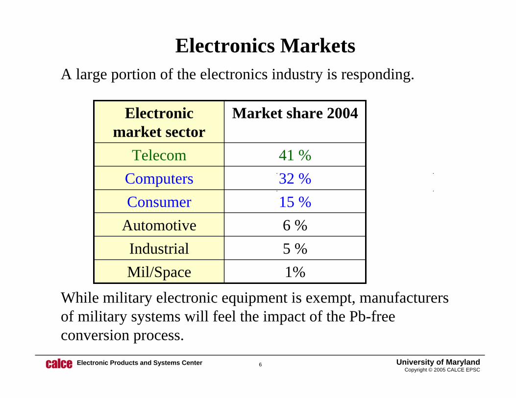
Electronics Markets
32 %Computers41 %Telecom
1%Mil/Space5 %Industrial6 %Automotive15 %Consumer
Market share 2004Electronic market sector
While military electronic equipment is exempt, manufacturers of military systems will feel the impact of the Pb-free conversion process.
A large portion of the electronics industry is responding.

University of MarylandCopyright © 2005 CALCE EPSC
Electronic Products and Systems Center 7
Challenges-General Pb-free Electronics
• No exact drop-in replacement for Pb-based materials/components.• Solder alloy selection may vary based on application.• Replacements likely to see wide adoption include
– SnAgCu – Reflow– SnAgCu or SnCu or SnCuNi – Wave– SnAgCu or SnAg - Rework
• Changes in component finishes, die attach materials, solders joints– Higher processing temperatures (pop-corning, board warpage,
delamination)– Compatibility with Pb-free processing (mixed technology)– Indirect failure mechanisms (tin whiskers, creep corrosion)– Solder joint reliability (durability, intermetallic growth)

University of MarylandCopyright © 2005 CALCE EPSC
Electronic Products and Systems Center 8
Solder material testing (constitutive and durability properties)NCMS (4 solders)Sn/3.9Ag/CuSn/AgSn/CuOthers (Sn-In/Bi/Zn/Al/Sb/3.0Ag/?)
PWB/component finish & interface integrity (OSP, Imm Au/Ag/Sn, Au/Ni, HASL, SnPb) (Mixed technology issues eg Pb-contamination; Post-aging tests)
Overstress (ball shear, PWB flexure, shock)Cyclic durability Noble platings and creeping corrosionWhiskering
Connector fretting corrosion Conductive and nonconductive adhesives
Soft particles (Au-plated polymers)No particles
Accelerated testing (SnAgCu, ?, multiple finishes, mixed tech, pre-aging)Thermal cycling/shockVibrationCombinationsMechanical shock/impactHumidity
Virtual qualification software/Model calibration Manufacturing/Rework QualityBusiness risk assessment, IP & liability issues
Virtual qualification, D
esign tradeoffsA
ccelerated testing, Health m
onitoring
CALCE Pb-free Roadmap---------96 97 98 99 00 01 02 03 04 05 06
http://www.calce.umd.edu/lead-free/projects.htm

University of MarylandCopyright © 2005 CALCE EPSC
Electronic Products and Systems Center 9
Mechanical Cyclic Fatigue Durability Properties of Pb-free Solder
solder layer(3mm x 1mm x 180 μm)
piezoelectric stack actuator
load frame
displacementtransducers
grips andshear specimen
load cell
High-precision, custom testing frame provides control necessary for testing of miniature-scale specimens
Cyclic durability Tests = f(amplitude, ramp rate,
dwell, temperature)
time, t (s)di
spl.,
δ(μ
m)
-25
-15
-5
5
15
25
-0.1 -0.05 0 0.05 0.1shear strain
shea
r str
ess
(MPa
)
Specimen HysteresisW
(mJ/mm3
)ISR
TSRStress
distribution within solder
joint
Cu Cu
Test SetupMiniature shear specimen
Model of Test setup
Objective: Determine cyclic fatigue durability properties of lead-free solder

University of MarylandCopyright © 2005 CALCE EPSC
Electronic Products and Systems Center 10
Durability Results Summary
• Low data scatter • Good agreement with published literature• Cyclic durability of Sn3.9Ag0.6Cu is
favorable to that of Sn63Pb37
fatigue cracksolder
• Active failure mechanisms are verified post-test using optical and electron microscopy
3+ load levels
strain rate:E-5, E-3,
E-1 s-1
tempera
ture:
25, 9
0, 15
0°C
plasticity
creep
0.01
0.1
1
10
100
1000
1 10 100 1000 10000 100000cycles to failure (50% load drop)
wor
k de
nsity
/cyc
le (m
J/m
m^3
SnAgCu: creep-min.
SnAgCu: creep-max.SnPb: creep-min.SnPb: creep-max.
N≅4-5000
Energy-based fatigue damage model
Fatigue test results for Sn3.9Ag0.6CuTMM Test Matrix
0.000.020.040.060.080.100.12
0 200 400 600 800 1000cycle
aver
age
shea
r stra
inra
nge.
012345678
wor
k di
ssip
atio
n/cy
cle
(mJ/
mm
3).
Amp/Ht. TSR ISR Wtrue Weng
Sample load drop data

University of MarylandCopyright © 2005 CALCE EPSC
Electronic Products and Systems Center 11
Accelerated Thermal Cycling
0
1000
2000
3000
1 2 3 4
cycl
es to
failu
re
Pb-free Pb-free/SnPb SnPb/Pb-free SnPb
PBGA TaBGA FlexBGA μBGA
The effect of Pb contamination in mixed technologies
Some observations from tests• Some early failures which appeared
to be anomalies occurred in mixed systems.
• FlexPBGA144 has two distinct populations (for inner & outer nets)
100.00 10000.01000.001.00
5.00
10.00
50.00
90.00
99.00 Probability - Weibull
Time, (t)
Unr
elia
bilit
y, F
(t)
Sn37Pb
flexBGATwo populations
μBGA
PBGA
TaBGA

University of MarylandCopyright © 2005 CALCE EPSC
Electronic Products and Systems Center 12
Durability of Solder under a Temperature Cycle Experimental data collected under C03-04 allowed CALCE to develop a preliminary rapid assessment model for Sn4.0-3.8Ag0.7Cu solder, released in the calcePWA software. Data consists mostly of standard test conditions (i.e. -40 to 125oC, -55 to 125oC, and 0 to 100oC) with little variation in dwell or mean temperature.
0%
1%
10%
100%
10 100 1000 10000 1000002 * Mean cycles to failure
Stra
in(%
)
Pb-free (SnAgCu)Sn37Pb
Pb-free outperforms SnPb
SnPb outperforms Pb-free

University of MarylandCopyright © 2005 CALCE EPSC
Electronic Products and Systems Center 13
Temperature Effect Study
Pending
Pending
Completed
Completed
Completed
Completed
Completed
Completed
Status
75*85158
85
75
125
100
75
125
100
MaxRange (˚C)
15
75*
75*
75*
15
15
15
Dwell Time (min)
157
-256
255
04
-253
252
01
Min Temp (˚C)
Test
Test Results for Tmean = 50oC, ΔT=100oC
Test Vehicle• 68-pin LCCC: 24mm × 24mm, Ceramic • 84-pin LCCC: 30mm × 30mm, Ceramic• Board: 130 x 93 x 2.5 mm, FR4
Solders Under Test• Indium SMQ 230 Sn95.43/Ag3.87/Cu0.7• Indium SMQ 230 Sn96.5/Ag3.5• Indium SMQ 92J Sn63/Pb37
Test Matrix
* Extended dwell at max temp only. Dwell at min temp fixed at 15 minutes

University of MarylandCopyright © 2005 CALCE EPSC
Electronic Products and Systems Center 14
Comparison of Time to Failure (68 IO Package)
For the Pb-free solders, increasing the average cyclic temperature showed adecrease in time to failure. As can be seen in the above chart, the behavior of the SnPb solder at the 100 and 125oC peak temperature shows non-monotonically decreasing behavior.
Peak Temperature (oC) (Dwell at Peak (min) )
Normalized

University of MarylandCopyright © 2005 CALCE EPSC
Electronic Products and Systems Center 15
Rapid Failure Assessment Software for Pb-free
On-going efforts in rapid assessment of printed wiring assemblies has resulted in a preliminary model for assessing failure of Pb-free (SnAgCu) solder package to board interconnects.
c
ffN
1
221
⎟⎟⎠
⎞⎜⎜⎝
⎛ Δ=
εγ
• Nf : mean number of cycles to failure
• Δγp : inelastic strain range• εf, c : material constants
• Qualitative graph represents CalcePWA model predictions for SnPb and SnAgCu solders.
• Crossing point likely to shift due to temperature cycle parameters (i.e. mean temperature, temperature range, dwell time, and ramp rate)

University of MarylandCopyright © 2005 CALCE EPSC
Electronic Products and Systems Center 16
plastic damage Nfpcreep damage Nfc
plastic work densitycreep work density
Total cycles to failure:fcfpft NNN
111+=5
2 Package Architecture
PWB
substrate overmold
Solder Joint
-50
-40
-30
-20
-10
0
10
20
30
0 0.005 0.01 0.015 0.02 0.025
equi. strain
equi
. str
ess (
MPa
)
Stress-Strain Hysteresis3
)
E-P Model4
0.01
0.1
1
10
100
1000
10 100 1000 10000 100000cycles to failure
wor
k de
nsity
(mj/m
m^
plasticcreep2
Test Vehicle
Energy-Partitioning Damage Model: Approach for Thermal Cycling
elastic-plastic
Constitutive Properties of Solders
Creep (primary & secondary)
1
ε
σ
Temperature
ε
t
T, σ

University of MarylandCopyright © 2005 CALCE EPSC
Electronic Products and Systems Center 17
Vibration Testing of Pb-free Assemblies
33Overstress test (Gf)
High temp storage 150ºC / 100 hours
33Stress level 2
(0.6Gf)
33Stress level 1
(0.8Gf)
SACOSP
SnPbHASL
Pre-treatment
Vibration Test Matrix Vibration Test Configuration
BGA LCCCPQFP
LCR
Strain gage wiring
All components are daisy-chained and monitored real-time for failure
Electrical connector for failure monitoring

University of MarylandCopyright © 2005 CALCE EPSC
Electronic Products and Systems Center 18
Time Domain Vibration Durability Assessment
0
30
60
Solder strain RDF
Strain range Δεeq
00. 00050. 001
0. 00150. 002
0. 00250. 003
0. 00350. 004
0. 0045
0 0. 0005 0. 001 0. 0015 0. 002
PCB curvature
Sold
er st
rain
3
Occ
urre
nce
rate
4 Vibration Durability Estimate based on Fatigue Damage
Cycles to failureIS
R
0. 001
0. 01
0. 1
1
10
100 1000 10000
SACSnPb
00. 0005
0. 0010. 0015
0. 0020. 0025
0. 0030. 0035
0. 0040. 0045
0 0. 0005 0. 001 0. 0015 0. 002
0. 000
0. 001
0. 002
0. 003
0. 004
0. 005
0. 006
0. 000 0. 001 0. 001 0. 002 0. 002 0. 003
0
0. 001
0. 002
0. 003
0. 004
0. 005
0 0. 0005 0. 001 0. 0015 0. 002
BGA LCCC Resistor
Mκ
ε M
2 Local Interconnect Stress Analysis (C04-02)
Solder strain as a fn of PWB curvature
Vibration Response
Occ
urre
nce
rate
Curvature range Δκ
PWB curvature Range Distribution function (RDF) from cycle counting1c
PWB curvature (κ ) history
-15
-10
-5
0
5
10
0 200 400 600 800 1000 1200 1400
Time (s)
Am
plitu
de (μ
ε)
1b
Global PWB Vibration Characterization1a
Mode 1
Mode n
Modal Analysis

University of MarylandCopyright © 2005 CALCE EPSC
Electronic Products and Systems Center 19
Impact Testing of Pb-free Assemblies
Specimen Design• Plastic Ball Grid Array
(PBGA) component• 256 balls, 1mm pitch, full
grid, daisy chained.• Eutectic 63/37 Sn-Pb
solder with OSP finish• 5.5”X4”X0.062” FR4
printed wiring board
Instrumentation• Strain gage on specimen• Accelerometer on fixture• Resistance monitoring system for failure detection
• 4 channel high speed data acquisition system
• LabView
Strain gage
PBGADaisy chain
terminals
Test Setup•Flexural loads•Inertial loads
Drops to Failure (N)
ε: PWA strainε: PWA strain ratea: Component acceleration
),,( afN εε=.

University of MarylandCopyright © 2005 CALCE EPSC
Electronic Products and Systems Center 20
Failure Analysis: High Speed FlexureBulk solder failure
Component
Sn-Pb Solder
Sn-Pb Solder
Board
FR4 board failureFailure site moves from bulk solder to intermetallic or copper trace as the PWA flexure rate increases.
Board
Component
Sn-PbSolder
Copper
Intermetallic failure
BoardCopper trace failure
Sn-PbSolder
Sn-PbSolder
Board
Component
Cu-SnIntermetallic
Crack
Sn-Pb Solder
Copper

University of MarylandCopyright © 2005 CALCE EPSC
Electronic Products and Systems Center 21
Electrochemical Migration in the Age of Pb-Free• What does Pb-Free mean to
electrochemical migration (ECM)?– New plating materials– New interconnect materials– New flux chemistries
• ECM and alternative platings– ENIG and ImSn dependent upon
plating quality– ImAg dependent upon electric
field• Sn-Based Alloys
– Use environment likely to be acidic with the presence of oxygen and halides
– Potential for order of magnitude increase in corrosion rate

University of MarylandCopyright © 2005 CALCE EPSC
Electronic Products and Systems Center 22
PWB Plating Study
Apply solder paste with stencil
Reflow at peak T=244°C
0.9Tm (168oC)
1000 hours
100 hours
10 hours
1000 hours
100 hours
10 hours
1000 hours
100 hours
10 hours
Place solder balls
Thermal Aging
Shear testing (25 balls)Cross-sectioning (2 balls)
Shear testing (25 balls)Cross-sectioning (2 balls)
0.85Tm (143.5oC) 0.8Tm (119oC)
Tm(Sn3.8Ag0.7Cu)=217oC(490K)
Five different platings from two manufacturers were reflow soldered with Sn3.8Ag0.7Cu to determine the intermetallic formation and shear strength.
OSPM, OSPT
HASLT
ImAgM , ImAgT
ImSnM , ImSnT
ENIGM , ENIGT
Samples
University of MarylandCopyright © 2005 CALCE EPSC
Electronic Products and Systems Center 23
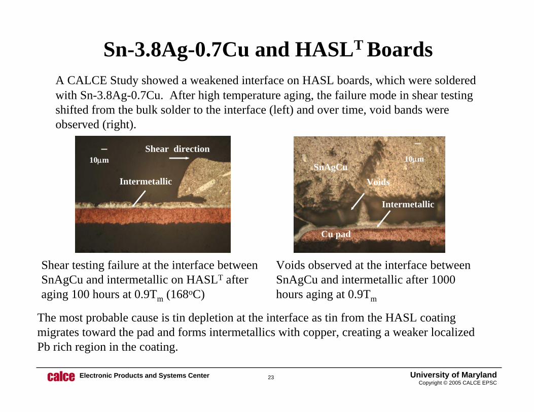
Sn-3.8Ag-0.7Cu and HASLT BoardsA CALCE Study showed a weakened interface on HASL boards, which were soldered with Sn-3.8Ag-0.7Cu. After high temperature aging, the failure mode in shear testing shifted from the bulk solder to the interface (left) and over time, void bands were observed (right).
Voids SnAgCu
Intermetallic
Cu pad
10μm
Voids observed at the interface between SnAgCu and intermetallic after 1000 hours aging at 0.9Tm
Intermetallic
Shear direction10μm
Shear testing failure at the interface between SnAgCu and intermetallic on HASLT after aging 100 hours at 0.9Tm (168oC)
The most probable cause is tin depletion at the interface as tin from the HASL coating migrates toward the pad and forms intermetallics with copper, creating a weaker localized Pb rich region in the coating.

University of MarylandCopyright © 2005 CALCE EPSC
Electronic Products and Systems Center 24
http://www.calce.umd.edu/lead-free/tin-whiskers
CALCE Tin Whisker Study
In addition to conducting multiple research projects on lead free solder issues this past year, CALCE joined with a number of companies to author an alert regarding the use of pure tin as a surface finish.
This alert was followed closely by a mitigation guide authored by CALCE with inputs from companies participating in the Tin Whisker Alert Working Group.

University of MarylandCopyright © 2005 CALCE EPSC
Electronic Products and Systems Center 25
CALCE Tin Whisker Team Studies (Roadmap)
Tin Whisker Alert and Related Risks
Tin Whisker Mitigation Guide
CALCE Tin Whisker Team2002
C03-30
Bending, current, solder dipping, and current study
TMTI Project-Solder
Dipping-
Monitoring finish selection of part suppliers; collecting, examining, and monitoring samples for whisker growth
C04-07
Update of tin whisker mitigation guide
-Continue to monitor tin whisker growth on the specimens-Focus on the specimens with Cu base
-Testing was conducted at Boeing/Raytheon
-Whisker could grow through some types of conformal coating
Tin whisker risk assessment methods and whisker growth studiesC05-O8
Solder Dip Annealing and Reflow Tests Conformal Coating
-No whisker was found at solder-dipped portion-Sample size was too small
-Initiated experiments with bright and matte tin over brass, Cu, and alloy 42.
-Initiated experiments to investigate the environmental conditions for tin whisker growth
Supplier survey

University of MarylandCopyright © 2005 CALCE EPSC
Electronic Products and Systems Center 26
Bending and Current Study
Bending method
Test flow chart
plastic container specimen
• Specimens– Size: 1.25”x0.5”x0.006”– Base material: Cu (Olin 194)– Plating: bright and matte tin (5µm thick)
• Pre-conditioning– Annealing at 150°C for one hour immediately after
the plating (half of the specimens)• Exposure
– Temperature/humidity (50°C/50%RH)• Current (1 Amp) - half of the specimens
– Room ambient• Whisker observation
– Specimens were periodically monitored (one week, 10 days, weekly afterwards).
– Specimen were taken out of the chamber only during the surface observation.
– Observation portions:
Bending
Annealing
Pure tin plated specimen
No-Annealing
Temperature/humidity(50°C/50%RH)
Room ambient
Current (1 Amp) No-current

University of MarylandCopyright © 2005 CALCE EPSC
Electronic Products and Systems Center 27
0
5
10
15
20
25
30
Whi
sker
Len
gth
(in m
ic
Bright tin
As-received 1 2 3 4 5 6 7 8 9 10 11weeks 8 months(bending)
0
10
20
30
40
50W
hisk
er L
engt
h (in
mic
ron Annealed, Non-current Non-annealed, Non-current
Annealed, Current Non-annealed, Current
Mattetin
As-received 1 2 3 4 5 6 7 8 9 10 11weeks 8 months(bending)
Maximum Whisker Length – Change with Time- Inner Curve -

University of MarylandCopyright © 2005 CALCE EPSC
Electronic Products and Systems Center 28
CALCE Pb-free Research 2005C05-01 Effects of Manufacturing Variables on Quality and Durability of Lead Free
Solder Joints (Continuation of C04-26)C05-02 Accelerated Qualification of SAC Assembly: Combined Temperature
Cycling & VibrationC05-40 Durability of Pb-free Electronic Interconnects Under Impact LoadingC05-03 Reliability of SnAgCu Solder for High Temperature/High Power
AssembliesC05-04 Experiments to Validate calcePWA Vibration Model (Pb/Sn & Sn/Ag/Cu)C05-05 Virtual Qualification of Pb-free Power Electronic AssembliesC05-06 Effect of Temperature Cycle on the Durability Lead Free Interconnects (Sn-
Ag-Cu and Sn-Ag) – ContinuedC05-07 Durability of Reworked Pb-free and Mixed (Pb-free/SnPb) Solders
InterconnectsC05-08 Tin Whisker Risk Metric and Mitigation Strategies for Electronic
AssembliesC05-09 Characterization of Moisture Absorption and Desorption FBGA Package in
Storage and Lead-Free Reflow Soldering ConditionsC05-10 Robustness of Ceramic Capacitors Assembled with Pb-Free SolderC05-11 Reliable Large-Area Pb-free Interconnects for Photovoltaic Cells Reliability
and Failure Assessment

University of MarylandCopyright © 2005 CALCE EPSC
Electronic Products and Systems Center 29
CALCE Pb-free Research Proposals 2006P06-H4 Determination of Kinematic Hardening Coefficient of Pb-free Solder P06-O5 Effect of Temperature Cycle on the Durability Pb-free
Interconnects(Sn96.5Ag3.0Cu0.5 and Sn99.2Cu0.7Ni0.1) P06-O7 Effect of Load Sequencing on Pb-free Solder Durability P06-B3 Experiments to Validate calcePWA Vibration Damage
Model (Pb/Sn & Sn/Ag/Cu) (continuation of C05-04) P06-A1 Effect of Manufacturing Variability on Reliability of Pb-free Solder
Joints (Continuation of C05-01) P06-A5 Reliable Large-Area Pb-free Interconnects for Photovoltaic
Cells (Continuation of C05-11) P06-A8 Effect of Characteristic Relaxation Time on Accelerated Thermal
Cycling Profiles for SAC Solders P06-Z1 Electrochemical Migration on Lead-free Printed Circuit Boards with No-
Clean Flux Technology P06-M2 Investigation of High Temperature Green Solder Materials P06-O4 Effect of Pb-free Reflow on Electrolytic and Box Capacitors P06-G4 Characterization of Tin Pest Formation in Pb-free Solder Joints

University of MarylandCopyright © 2005 CALCE EPSC
Electronic Products and Systems Center 30
Long-term Pb-free Reliability Study
• CALCE EPSC is conducting a comprehensive long-term lead-free reliability study supported by many companies.
• The goal of the study is to determine critical information related to the long-term (5-15 years) reliability of lead-free assemblies.
• This is a great opportunity for companies to benefit from these studies in a cost-effective way.
• Participation cost: $45K

University of MarylandCopyright © 2005 CALCE EPSC
Electronic Products and Systems Center 31
CALCE Long-term Pb-free Reliability Study Experimental Matrix
Temp. cycling + vibration
Temp. cycling (-40ºC to 125ºC)
HAST (130ºC / 85%RH / 672 hours) + Bias (for corrosion test structure)
Not applicable
Vibration testNone (Control)
SACSACSACSACSn-Pb
Low temp. storage (-55ºC/1000 hours)
Vibration testHigh temp. storage (150ºC/100 hours)
None
None
Vibration test
Vibration testLow temp. storage (-55ºC/500 hours)
Vibration testHigh temp. storage (150ºC/350 hours)
OSPENIGImmersion Sn
Immersion Ag
HASL
Solder and PCB pad finishAccelerated stressing
Pre-treatment
University of MarylandCopyright © 2005 CALCE EPSC
Electronic Products and Systems Center 32
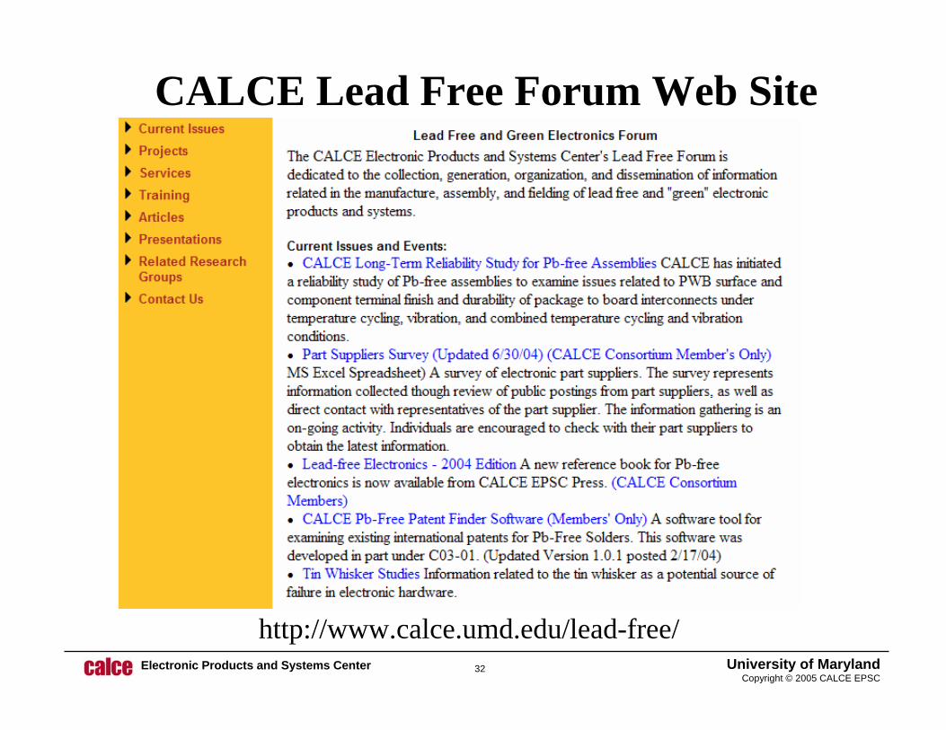
http://www.calce.umd.edu/lead-free/
CALCE Lead Free Forum Web Site

University of MarylandCopyright © 2005 CALCE EPSC
Electronic Products and Systems Center 33
Pb-Free Resources
Chapter 1 Lead-free Electronics: Overview
Chapter 2 Lead-free Alloys: OverviewChapter 3 Constitutive Properties and
Durability of Lead-free SoldersChapter 4 Interfacial Reactions and
Performance of Lead-free JointsChapter 5 Lead-free ManufacturingChapter 6 Component-level Issues in
Lead-free ElectronicsChapter 7 Conductive AdhesivesChapter 8 Lead-free Separable Contacts
and ConnectorsChapter 9 Intellectual PropertyChapter 10 Costs to Lead-free MigrationChapter 11 Lead-free Technologies in the
Japanese Electronics Industry
http://www.calce.umd.edu/general/published/books/books.html

University of MarylandCopyright © 2005 CALCE EPSC
Electronic Products and Systems Center 34
CALCE Contact Information• Dr. Michael Pecht, Center Director, Founder and Technical Advisor, Reliability &
Supply Chain Policies 301-405-5323, [email protected]
• Dr. Michael Osterman, Consortium Operations Director, Software Development 301-405-8023, [email protected]
• Dr. Abhijit Dasgupta, Interconnect Reliability, Accelerated Testing301-405-5251, [email protected]
• Dr. Ji Wu, Connecters & IC Sockets, Lead-Free Materials 301-405-0765, [email protected]
• Dr. Bongtae Han, Stress Measurement , Optical Measurement Techniques 301-405-5255, [email protected]
• Dr. Patrick McCluskey, Power Electronics, Component Reliability301-405-0279, [email protected]
• Dr. Diganta Das, Parts Selection & Management301-405-5323, [email protected]


