Passive and Active Hybrid Integrated EMI Filters · 2019-08-06 · Passive and Active Hybrid...
11
Passive and Active Hybrid Integrated EMI Filters Juergen Biela, Member, IEEE, Alexander Wirthmueller, Roman Waespe, Marcello Lobo Heldwein, Member, IEEE, Klaus Raggl, Member, IEEE, and Johann W. Kolar, Senior Member, IEEE „This material is posted here with permission of the IEEE. Such permission of the IEEE does not in any way imply IEEE endorsement of any of ETH Zürich’s products or services. Internal or personal use of this material is permitted. However, permission to reprint/republish this material for advertising or promo- tional purposes or for creating new collective works for resale or redistribution must be obtained from the IEEE by writing to [email protected]. By choosing to view this document you agree to all provisions of the copyright laws protecting it.”
Transcript of Passive and Active Hybrid Integrated EMI Filters · 2019-08-06 · Passive and Active Hybrid...

Passive and Active Hybrid Integrated EMI Filters
Juergen Biela, Member, IEEE, Alexander Wirthmueller, Roman Waespe, Marcello Lobo Heldwein, Member, IEEE, Klaus Raggl, Member, IEEE, and Johann W. Kolar, Senior Member, IEEE
„This material is posted here with permission of the IEEE. Such permission of the IEEE does not in any way imply IEEE endorsement of any of ETH Zürich’s products or services. Internal or personal use of this material is permitted. However, permission to reprint/republish this material for advertising or promo-tional purposes or for creating new collective works for resale or redistribution must be obtained from the IEEE by writing to [email protected]. By choosing to view this document you agree to all provisions of the copyright laws protecting it.”

1340 IEEE TRANSACTIONS ON POWER ELECTRONICS, VOL. 24, NO. 5, MAY 2009
Passive and Active Hybrid Integrated EMI FiltersJuergen Biela, Member, IEEE, Alexander Wirthmueller, Roman Waespe, Marcello Lobo Heldwein, Member, IEEE,
Klaus Raggl, Member, IEEE, and Johann W. Kolar, Senior Member, IEEE
Abstract—Two new planar integrated electromagnetic interfer-ence (EMI) filter structures that reduce the filter volume and thatare based on standard printed circuit board (PCB) process tech-nology are presented in this paper. First, a passive integrated EMIfilter is presented, which results in a volume reduction of 24% com-pared to the discrete solution. However, this filter requires a planarferrite core for the common-mode inductor. In order to eliminatethe ferrite core and reduce the filter volume further (−40% ver-sus discrete filter), a passive integrated structure is combined withan active EMI filtering circuit. The transfer function, the volume,and the losses of the discrete and the two integrated filters, whichare designed for a 600 W power-factor-corrected converter, arecompared.
Index Terms—Active filter, electromagnetic interference (EMI)filter, integrated passives, printed circuit board (PCB) inductor.
I. INTRODUCTION
THE PURSUIT of obtaining higher power density ac/dc anddc/dc converters leads to increasing switching frequencies
in order to reduce the size of the energy storage elements. Theseenergy storage elements usually influence the overall size ofa converter significantly. This has resulted in the developmentof electromagnetically integrated structures [1] that combineseveral functions in one passive component.
Due to increasing switching frequencies, conducted emis-sions from 150 kHz to 30 MHz have increased. Thus, the elec-tromagnetic interference (EMI) filter has also become a signif-icant part of the converter in terms of size and cost. For thisreason, some electromagnetically integrated EMI filter struc-tures [2] and [4] and also active EMI filters [5] and [6] havebeen proposed.
In this paper, two new planar EMI filter structures are pre-sented that allow a significant reduction of the filter volume.These structures are integrated in a printed board circuit (PCB),which could be manufactured using a cost-saving standard PCBmanufacturing process.
Manuscript received October 2, 2008; revised November 20, 2008. Currentversion published May 6, 2009. This paper was presented in part at the AppliedPower Electronics Conference and Exposition (APEC), Dallas, TX, February2006. Recommended for publication by Associate Editor P. Tenti.
J. Biela, R. Waespe, K. Raggl, and J. W. Kolar are with the Power Elec-tronic Systems Laboratory, Swiss Federal Institute of Technology Zurich (ETHZurich), Zurich 8092, Switzerland (e-mail: [email protected]; [email protected]; [email protected]).
A. Wirthmueller was with the Power Electronic Systems Laboratory,Swiss Federal Institute of Technology Zurich (ETH Zurich), Zurich 8092,Switzerland. He is now with Columbia University, New York, NY 10027-70031USA (e-mail: [email protected]).
M. L. Heldwein is with the Federal University of Santa Catarina,Florianopolis 88040-970, Brazil (e-mail: [email protected]).
Color versions of one or more of the figures in this paper are available onlineat http://ieeexplore.ieee.org.
Digital Object Identifier 10.1109/TPEL.2009.2012404
Fig. 1. Circuit diagram of a 600 W PFC.
TABLE ISPECIFICATION OF PFC CONVERTER
With the first filter structure, all inductor windings and allcapacitors except for a large differential-mode (DM) capacitorare integrated in the PCB. The DM capacitor is realized by aparallel connection of X2 SMD-X7R capacitors. For the largeinductance value of the common-mode (CM) choke, a planarferrite core is needed, although the overall filter has a very lowprofile (height <9.5 mm) and a low volume (≈25% volume re-duction in comparison to a discrete solution). This filter is calleda passive hybrid integrated EMI filter due to the combination ofintegrated and discrete passive components.
In a second step, the passive integrated structure is combinedwith an analog amplifier (active EMI filter). With the amplifierstage, the required inductance and capacitance values of thecomponents decrease significantly, so that no additional ferritecore is needed. The components of the active filter are mountedon top of the PCB, where the passive filter is integrated. Thisnew approach results in a very compact construction (≈40%volume reduction in comparison to a discrete solution) and iscalled active hybrid integrated EMI filter.
The two proposed filter structures are designed for a 600 Wpower-factor-corrected (PFC) converter intended for informa-tion technology (IT) applications (cf., Fig. 1) with the specifica-tion given in Table I. In Section II of this paper, the discrete EMIfilter for the PFC converter is described for comparing the newstructures with a conventional filter. The structure of the passive
0885-8993/$25.00 © 2009 IEEE
BIELA et al.: PASSIVE AND ACTIVE HYBRID INTEGRATED EMI FILTERS 1341
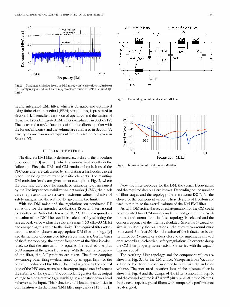
Fig. 2. Simulated emission levels of DM noise, worst-case values inclusive of6 dB safety margin, and limit values (light-colored curve: CISPR 11 class A QPlimit).
hybrid integrated EMI filter, which is designed and optimizedusing finite-element method (FEM) simulations, is presented inSection III. Thereafter, the mode of operation and the design ofthe active hybrid integrated EMI filter is explained in Section IV.The measured transfer functions of all three filters together withthe losses/efficiency and the volume are compared in Section V.Finally, a conclusion and topics of future research are given inSection VI.
II. DISCRETE EMI FILTER
The discrete EMI filter is designed according to the proceduredescribed in [10] and [11], which is summarized shortly in thefollowing. First, the DM- and CM-conducted emissions of thePFC converter are calculated by simulating a high-order circuitmodel including the relevant parasitic elements. The resultingDM emission levels are given as an example in Fig. 2, wherethe blue line describes the simulated emission level measuredby the line impedance stabilization networks (LISN), the blackcurve represents the worst-case maximum values inclusive ofsafety margin, and the red and the green line the limits.
With the DM noise and the regulations on conducted RFemissions for the intended application [Special InternationalCommittee on Radio Interference (CISPR) 11], the required at-tenuation of the DM filter could be calculated by selecting thelargest peak value within the relevant range (150 kHz–30 MHz)and comparing this value to the limits. The required filter atten-uation is used to choose an appropriate DM filter topology [9]and the number of connected filter stages in series. On the basisof the filter topology, the corner frequency of the filter is calcu-lated, so that the attenuation is equal to the required one plus6 dB margin at the given frequency. With the corner frequencyof the filter, the LC products are given. The filter dampingis—among other things—determined by an upper limit for theoutput impedance of the filter. This limit is given by the controlloop of the PFC converter since the output impedance influencesthe stability of the system. The controller regulates the dc outputvoltage to a constant voltage resulting in a constant power loadbehavior at the input. This behavior could lead to instabilities incombination with the mains/EMI filter impedances [12], [13].
Fig. 3. Circuit diagram of the discrete EMI filter.
Fig. 4. Insertion loss of the discrete EMI-filter.
Now, the filter topology for the DM, the corner frequencies,and the required damping are known. Depending on the numberof filter stages and the topology, there are some DOFs for thechoice of the component values. These degrees of freedom areused to minimize the overall volume of the DM EMI filter.
As with DM noise, the required attenuation for the CM couldbe calculated from CM noise simulation and given limits. Withthe required attenuation, the filter topology is selected and thecorner frequency of the filter is calculated. Since the Y-capacitorsize is limited by the regulations—the current to ground mustnot exceed 3 mA at 50 Hz—the value of the inductance is de-termined for Y-capacitor values close to the maximum allowedones according to electrical safety regulations. In order to dampthe CM filter properly, some resistors in series with the capaci-tors are added.
The resulting filter topology and the component values areshown in Fig. 3. For the CM choke, Vitroperm from Vacuum-schmelze has been chosen in order to minimize the inductorvolume. The measured insertion loss of the discrete filter isshown in Fig. 4 and the design of the filter is shown in Fig. 5,and the overall volume is 47.4 cm3 (48 mm× 38 mm× 26 mm).In the next step, integrated filters with comparable performanceare designed.
1342 IEEE TRANSACTIONS ON POWER ELECTRONICS, VOL. 24, NO. 5, MAY 2009
Fig. 5. Photograph of the discrete EMI filter.
TABLE IIPARAMETERS OF THE PASSIVE HYBRID EMI FILTER
III. PASSIVE HYBRID EMI FILTERS
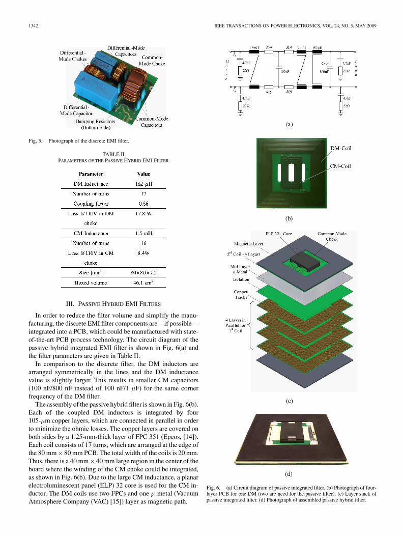
In order to reduce the filter volume and simplify the manu-facturing, the discrete EMI filter components are—if possible—integrated into a PCB, which could be manufactured with state-of-the-art PCB process technology. The circuit diagram of thepassive hybrid integrated EMI filter is shown in Fig. 6(a) andthe filter parameters are given in Table II.
In comparison to the discrete filter, the DM inductors arearranged symmetrically in the lines and the DM inductancevalue is slightly larger. This results in smaller CM capacitors(100 nF/800 nF instead of 100 nF/1 µF) for the same cornerfrequency of the DM filter.
The assembly of the passive hybrid filter is shown in Fig. 6(b).Each of the coupled DM inductors is integrated by four105-µm copper layers, which are connected in parallel in orderto minimize the ohmic losses. The copper layers are covered onboth sides by a 1.25-mm-thick layer of FPC 351 (Epcos, [14]).Each coil consists of 17 turns, which are arranged at the edge ofthe 80 mm× 80 mm PCB. The total width of the coils is 20 mm.Thus, there is a 40 mm× 40 mm large region in the center of theboard where the winding of the CM choke could be integrated,as shown in Fig. 6(b). Due to the large CM inductance, a planarelectroluminescent panel (ELP) 32 core is used for the CM in-ductor. The DM coils use two FPCs and one µ-metal (VacuumAtmosphere Company (VAC) [15]) layer as magnetic path.
Fig. 6. (a) Circuit diagram of passive integrated filter. (b) Photograph of four-layer PCB for one DM (two are need for the passive filter). (c) Layer stack ofpassive integrated filter. (d) Photograph of assembled passive hybrid filter.
BIELA et al.: PASSIVE AND ACTIVE HYBRID INTEGRATED EMI FILTERS 1343
Fig. 7. (a) Diagram of coupled coils. (b) Design of the coils.
The damping of the passive integrated filter mainly resultsfrom the frequency-dependent resistors R(f), which representthe high-frequency losses of the coils due to skin and proximityeffect. The geometry of the coils is designed so that the dc lossesare low, but the high-frequency losses are high enough to dampthe filter. The damping elements at the input and output of thefilter remain in order to attenuate oscillations caused by the lineor the input impedance of the converter. The capacitors and theresistors of the damping elements could also be integrated in thePCB using dielectric and resistive layers (e.g., HiK-material andOHMEGA-PLY/Carbon Paste, respectively [16], [17]). In orderto simplify the testing of the filter, the capacitors and resistorsof the damping network are realized by surface mount device(SMD) components in the prototype.
A. Design of Coupled Inductors
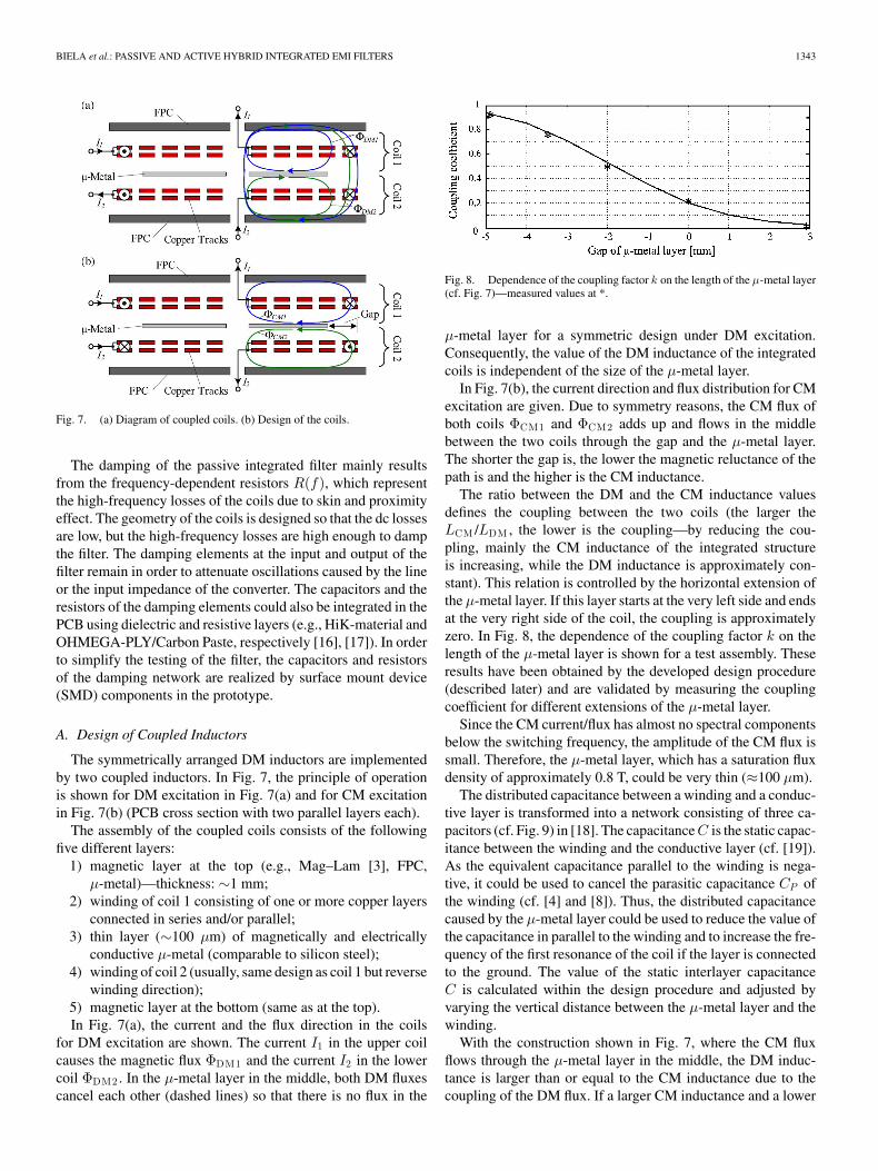
The symmetrically arranged DM inductors are implementedby two coupled inductors. In Fig. 7, the principle of operationis shown for DM excitation in Fig. 7(a) and for CM excitationin Fig. 7(b) (PCB cross section with two parallel layers each).
The assembly of the coupled coils consists of the followingfive different layers:
1) magnetic layer at the top (e.g., Mag–Lam [3], FPC,µ-metal)—thickness: ∼1 mm;
2) winding of coil 1 consisting of one or more copper layersconnected in series and/or parallel;
3) thin layer (∼100 µm) of magnetically and electricallyconductive µ-metal (comparable to silicon steel);
4) winding of coil 2 (usually, same design as coil 1 but reversewinding direction);
5) magnetic layer at the bottom (same as at the top).In Fig. 7(a), the current and the flux direction in the coils
for DM excitation are shown. The current I1 in the upper coilcauses the magnetic flux ΦDM1 and the current I2 in the lowercoil ΦDM2 . In the µ-metal layer in the middle, both DM fluxescancel each other (dashed lines) so that there is no flux in the
Fig. 8. Dependence of the coupling factor k on the length of the µ-metal layer(cf. Fig. 7)—measured values at *.
µ-metal layer for a symmetric design under DM excitation.Consequently, the value of the DM inductance of the integratedcoils is independent of the size of the µ-metal layer.
In Fig. 7(b), the current direction and flux distribution for CMexcitation are given. Due to symmetry reasons, the CM flux ofboth coils ΦCM1 and ΦCM2 adds up and flows in the middlebetween the two coils through the gap and the µ-metal layer.The shorter the gap is, the lower the magnetic reluctance of thepath is and the higher is the CM inductance.
The ratio between the DM and the CM inductance valuesdefines the coupling between the two coils (the larger theLCM /LDM , the lower is the coupling—by reducing the cou-pling, mainly the CM inductance of the integrated structureis increasing, while the DM inductance is approximately con-stant). This relation is controlled by the horizontal extension ofthe µ-metal layer. If this layer starts at the very left side and endsat the very right side of the coil, the coupling is approximatelyzero. In Fig. 8, the dependence of the coupling factor k on thelength of the µ-metal layer is shown for a test assembly. Theseresults have been obtained by the developed design procedure(described later) and are validated by measuring the couplingcoefficient for different extensions of the µ-metal layer.
Since the CM current/flux has almost no spectral componentsbelow the switching frequency, the amplitude of the CM flux issmall. Therefore, the µ-metal layer, which has a saturation fluxdensity of approximately 0.8 T, could be very thin (≈100 µm).
The distributed capacitance between a winding and a conduc-tive layer is transformed into a network consisting of three ca-pacitors (cf. Fig. 9) in [18]. The capacitance C is the static capac-itance between the winding and the conductive layer (cf. [19]).As the equivalent capacitance parallel to the winding is nega-tive, it could be used to cancel the parasitic capacitance CP ofthe winding (cf. [4] and [8]). Thus, the distributed capacitancecaused by the µ-metal layer could be used to reduce the value ofthe capacitance in parallel to the winding and to increase the fre-quency of the first resonance of the coil if the layer is connectedto the ground. The value of the static interlayer capacitanceC is calculated within the design procedure and adjusted byvarying the vertical distance between the µ-metal layer and thewinding.
With the construction shown in Fig. 7, where the CM fluxflows through the µ-metal layer in the middle, the DM induc-tance is larger than or equal to the CM inductance due to thecoupling of the DM flux. If a larger CM inductance and a lower

1344 IEEE TRANSACTIONS ON POWER ELECTRONICS, VOL. 24, NO. 5, MAY 2009
Fig. 9. Equivalent network for a distributed capacitance between a windingand a conductive layer according to [18].
Fig. 10. Flowchart of the design procedure for the integrated coils.
DM inductance are needed, the winding direction of one coilhas to be changed. In this case, a thicker magnetic middle layer(twice the thickness of the outer magnetic layer) is needed,because the relatively large DM flux flows through the mid-dle layer. The achievable maximum values for the CM and theDM inductances are the same for both design possibilities, ifthe distance between two magnetic layers above and below onePCB (i.e., the gap) is the same. Consequently, the design withthe changed winding direction leads to an increased volume andlarger magnetic losses for the same maximum achievable induc-tance values, and should only be used in case a CM inductanceis needed, which is larger than the DM one.
B. Design Procedure
The integrated inductors of the EMI filter are designed usingan automated design procedure, whose flow chart is given inFig. 10. This procedure, which is based on FEM simulations
Fig. 11. DM—finite-element simulation of passive hybrid integrated EMIfilter.
(COMSOL) and analytic calculations, will be shortly explainedin the following.
At the beginning of the procedure, different parameters likethe number of layers in the PCB NL , the number of parallelconnected layers NLP , PCB size B × T , the vertical distancebetween the layers tν , etc., must be specified by the user. Theseparameters are not varied within the design procedure since theymainly depend on requirements not related to the filter itself. Onthe other hand, there are parameters like the number of turns N ,the PCB width wTrack and distance wTrack , the thickness tCof the magnetic layers, etc., which could be varied in order tooptimize the design.
With the parameters given in MATLAB, input files for FEMsimulations describing the geometry and boundary conditionsare automatically generated by the program. In the next step,FEM simulations are carried out by the program for differentsetups (CM and DM excitation, different voltagedistributions)—cf. Fig. 11. On the basis of the magneticand electric energies, the inductance and capacitance valuesare calculated. Furthermore, the magnetic field distribution isused to calculate the HF resistances of the coils analytically.Thereafter, the calculated values are transformed into equivalentcircuit values of the EMI filter.
The described design routine offers the possibility to be usedwithin an optimization routine, which varies, for example, thenumber of turns and the design of the tracks in order to minimizethe filter volume or maximize the efficiency.
IV. ACTIVE HYBRID EMI FILTER
The discrete and also the passive hybrid EMI filters requirea large CM inductance because the value of the Y-capacitanceis limited by regulations and the corner frequency of the filteris low due to the CM emission level. Since the amplitude ratioof the high-frequency CM current and the DM current at theline frequency is usually relatively small, the volume of theCM inductor could be reduced by using an active filter. Thisactive EMI filter consists of two small CM inductors, two 20 nFcapacitors, a measurement network, and an analog amplifier, asshown in Fig. 12(a) (cf. [20]).
With the measurement network, the CM voltage VCM causedby the converter/load is measured via the two 1-nF capacitors.The CM voltage is amplified by an analog class-A amplifier,which injects an inverted CM current via the two 22-nF ca-pacitors into the filter network. Thus, the CM current resulting

BIELA et al.: PASSIVE AND ACTIVE HYBRID INTEGRATED EMI FILTERS 1345
Fig. 12. (a) Circuit diagram of the active hybrid integrated EMI filter.(b) Design of the active hybrid integrated EMI filter.
from the load is canceled/reduced by the active filter. Due tothe limited gain of the amplifier and nonideal components, theamplitude of the CM voltage/current is only reduced by approx-imately 20 dB in the best case.
Moreover, the limited bandwidth of the amplifier requires areduction of the gain at higher frequencies in order to guaranteethe stability of the system. This also results in a decline of the CMvoltage/current cancelation at higher frequencies. In the limitedfrequency range from approximately 100 kHz up to 6 MHz,where the voltage/current cancelation is working, the effectiveCM capacitance is increased very much by the amplifier. Thus,a smaller CM inductance can be used to obtain the same cornerfrequency/attenuation as for the CM filter of the discrete/passivehybrid filter.
The decline of the attenuation due to the limited amplifierbandwidth is not critical, because the effective impedance of alarge CM choke also decreases with increasing frequency due tothe parasitic capacitance that causes a parallel resonant behaviorof the choke at higher frequencies.
The two CM inductors needed for the active EMI filter areintegrated in the PCB, as described in the previous section.The final design of the complete active hybrid integrated filteris shown in Fig. 12(b), where the components of the activefilter are mounted on top of the PCB. Below the active filter,the capacitances for measuring the CM voltage and injectingthe CM current as well as the relatively small capacitances for
TABLE IIIMATERIALS FOR CAPACITANCE INTEGRATION
Fig. 13. (a) Picture of assembled active hybrid EMI filter. (b) Picture of thePCB of one layer. (c) 3-D drawing of final assembly of active filter.
damping resonances at the input and the output of the filter canbe integrated. Due to the planar design, these capacitors showlow equivalent series resistance (ESR) and equivalent seriesinductance (ESL). In Table III, some dielectric materials forintegrating capacitances into PCBs are shown.
Due to the relatively low permittivity of these materials, thelarge capacitors for the DM CDM still have to be realized asSMD capacitors that are mounted on top of the PCB besides theactive filter components.
In Fig. 13(a), the examined prototype of the coupled coilsfor the active filter is shown. It consists of four layers of FPC302 from Epcos with a thickness of approximately 1.3 mm, fourPCBs, each with four 105 µm layers of copper for the coils[cf. Fig. 13(b)], and two layers of µ-metal. On the left-handside, the terminals of the µ-metal layers are shown with whichthe layers could be connected to ground in order to reduce theparasitic capacitance. Below the pictures, a 3-D drawing of thefinal assembly of the integrated active hybrid filter is shown inFig. 13(c). In Table IV, the technical parameters of the activeEMI filter are listed.
1346 IEEE TRANSACTIONS ON POWER ELECTRONICS, VOL. 24, NO. 5, MAY 2009
TABLE IVPARAMETER OF ACTIVE HYBRID EMI FILTER
Fig. 14. Circuit for the measurement of the transfer (U2 /U1 ) function (filterattenuation) and the input impedance.
Fig. 15. Comparison between the DM attenuation/transfer function (U2 /U1 )and insertion loss of the active hybrid filter.
Fig. 16. (a) Transfer function of the passive filter for CM with (with GND) andwithout connection of the µ-metal layer to ground (without GND) and for DM.(b) Input impedance of the filter at the load side for CM and DM with phase(dashed lines).
Fig. 17. (a) Transfer function of the active filter for CM with (with AMP) andwithout amplifier (without AMP) and for DM. (b) Input impedance of the filterat the load side for CM with (with AMP) and without amplifier (without AMP)with phase (dashed lines). (c) Input impedance of the filter at the load side forDM with phase (dashed lines).
Fig. 18. New design of the CM choke.
V. COMPARISON OF THE EMI FILTERS
In order to compare the performance of the different filters,measured transfer functions, losses, and volume of the discrete,the passive, and the active hybrid filters are presented in thefollowing.

BIELA et al.: PASSIVE AND ACTIVE HYBRID INTEGRATED EMI FILTERS 1347
TABLE VCALCULATED AND MEASURED PARAMETERS OF THE THREE COMPARED EMI FILTERS
Usually, insertion loss measurements, i.e., the ratioU2/UNoise , are used to characterize EMI filters. However, thesemeasurements also include the attenuation that results from thesource impedance of the measurement circuit (usually 50 Ω) andthe filter capacitors (cf. Fig. 14). The source/internal impedanceof the noise source and also the additional attenuation dependvery much on the converter topology and the design of the con-verter. In order to obtain information about the filter attenuationthat is independent of the source impedance, the transfer func-tion, i.e., the ratio U2/U1 , is used in the following. The inputvoltage of the filter U1 for a given source impedance could becalculated with the input impedance ZIN of the EMI filter, whichis also presented in the following. The additional attenuation be-cause of the source impedance could be seen in Fig. 15, wherethe DM insertion loss and the transfer function for the activefilter are plotted in the same graph.
In Fig. 16, the CM and the DM attenuation and the inputimpedance of the passive hybrid filter are given, where the twocurves for the CM show the different attenuation of the filterwhen the µ-metal layer is connected to ground or free floating.Due to the additional parasitic capacitances (cf. Fig. 9), theHF behavior of the filter is improved. The resonant peak ofthe CM attenuation between 400 and 500 kHz results from thecharacteristic frequency of the CM choke.
Due to the large source impedance of the PFC converter (boostinductor: 187 µH—cf. Fig. 1), the DM attenuation of the passivefilter increases very much in the frequency range from 100 kHzto 1 MHz, since the input impedance of the filter is relativelylow in this region. For example, at 100 kHz, approximately ad-ditional 20 dB results from the large source impedance resultingin an effective attenuation larger than 40 dB for DM at 100 kHz.
In the considered frequency range, the input impedance of theactive filter for DM is even lower than that of the passive filter,which leads to a larger additional damping due to the sourceimpedance (cf., Fig. 17). Consequently, the DM attenuation ofthe two integrated filters is comparable to that of the discretefilter and even exceeds it a bit.
The comparatively low resonance frequency of the CM chokeof the passive integrated filter results in a CM attenuation curvethat is not as good as that of the discrete filter. The reason for thisis the parasitic capacitances resulting from the planar windingdesign. A possible alternative design of the CM choke, whichleads to reduced parasitic capacitances and also lower losses,is shown in Fig. 18, where the core is integrated in the PCBby magnetic layers and the winding consists of wire or in caseof low-power applications of PCB tracks. For the considered600-W PFC system, the winding must be made of wires in orderto keep the efficiency high. Since this would require specialmanufacturing technologies, which are out of the focus of thisproject, this approach is not further investigated.
In Fig. 17(a), the CM attenuation of the active integrated filteris shown, where it could be seen that the amplifier results in anadditional attenuation of 15–20 dB in the frequency range from400 kHz to 4 MHz. The resonant peak at approximately 160 kHzis caused by the limited gain of the amplifier. As simulationsshow, the gain could be increased by using transistors with ahigher transition frequency in the power stage of the amplifier.
The resonant peak around 2 MHz in the CM attenuation of theactive integrated filter is caused by the characteristic frequencyof the integrated coils.
In Table V, the volume, the losses, and the efficiency ofthe three EMI filters are given. The values in the “modified”columns result from using Vacoflux 48 (VAC [15]), which has asaturation flux density of 2 T, instead of FPC 351/302 [14] as themagnetic layer. The basic design of the inductors is the same forboth materials, just the higher possible maximal flux density isutilized to reduce the number of turns and therewith the losses.As can be seen, the losses and the volume of the integrated filterscan be reduced very much so that the efficiency of the integratedfilters is comparable to that of the discrete filter, but the volumeis reduced by more than 40%.
The presented approach for the passive hybrid filter, which isthe more promising integration method if burst test and high-voltage spikes at the mains are considered, is also applied to an

1348 IEEE TRANSACTIONS ON POWER ELECTRONICS, VOL. 24, NO. 5, MAY 2009
TABLE VIPARAMETER OF THE 300W PASSIVE HYBRID EMI-FILTER
Fig. 19. (a) Photograph of the discrete and (b) the integrated EMI filter of a300-W PFC. The integrated filter utilized an ELP22 core, the CM choke, andhas in total eight 100 µ copper, two µ-metal, and four magnetic layers, whereeach inductor consists of only two copper layers instead of the four layers ofthe 600-W passive hybrid filter.
EMI filter for a 300-W PFC system. This PFC system is oper-ating at a switching frequency of 200 kHz, and is designed foran output voltage of 400 V and an input voltage of 230 V(+10%/−15%). The parameters of the filter are given inTable VI, and in Fig. 19, photographs of the discrete and theintegrated solution are given. The volume of the discrete filteris 22 cm3 , so that the volume could be decreased by 27% byintegrating the filter in the PCB. This reduction is similar to the600-W filter, where the volume could be shrunk by roughly 23%for the original design where ferrite foil has been utilized.
VI. CONCLUSION
The EMI filter is a significant part of a converter in termsof size and cost. Thus, the size of EMI filters must be reducedand the manufacturing simplified in order to increase the powerdensity and reduce the cost of converter systems.
In this paper, a design procedure and measurement results fortwo different integration approaches—a passive hybrid integra-tion in a PCB and an active hybrid integration with an active EMIfilter—are presented. The filter inductors are integrated into aPCB board that could be manufactured with standard PCB man-ufacturing technology. Due to the integration, the filter volumecould be reduced by approximately 40% while maintaining ahigh efficiency.
REFERENCES
[1] J. T. Strydom, “Electromagnetic design of integrated resonator-transformers,” Ph.D. dissertation, Rand Afrikaans Univ., Johannesburg,South Africa, 2001.
[2] J. D. van Wyk, F. C. Lee, Z. Liang, R. Chen, S. Wang, and B. Lu, “Integrat-ing active, passive and EMI-filter functions in power electronic system: Acase study of some technologies,” IEEE Trans. Power Electron., vol. 20,no. 3, pp. 523–536, May 2005.
[3] E. Waffenschmidt, B. Ackermann, and J. A. Ferreira, “Design methodand material technologies for passives in printed circuit board embeddedcircuits,” IEEE Trans. Power Electron., vol. 20, no. 3, pp. 576–584, May2005.
[4] R. Chen, J. D. van Wyk, S. Wang, and W. G. Odendaal, “Improvingthe characteristics of integrated EMI filters by embedded conductive lay-ers,” IEEE Trans. Power Electron., vol. 20, no. 3, pp. 611–619, May2005.
[5] T. Farkas and M. F. Schlecht, “Viability of active EMI filters for utilityapplications,” IEEE Trans. Power Electron., vol. 9, no. 3, pp. 328–337,May 1994.
[6] L. Lawhite and M. F. Schlecht, “Design of active ripple filters for powercircuits operating in the 1–10 MHz range,” IEEE Trans. Power Electron.,vol. 3, no. 3, pp. 310–317, Jul. 1988.
[7] T. C. Neugebauer and D. J. Perrault, “Filters with inductance cancellationusing printed circuit board transformers,” IEEE Trans. Power Electron.,vol. 19, no. 3, pp. 591–602, May 2004.
[8] T. C. Neugebauer and D. J. Perrault, “Parasitic capacitance cancellation infilter inductors,” in Proc. 35th IEEE Power Electron. Spec. Conf. (PESC2004), Aachen, Germany, Jun., pp. 3102–3107.
[9] M. J. Nave, “A novel differential mode rejection network for conductedemissions diagnostics,” in Proc. IEEE 1989 Nat. Symp. Electromagn.Compat., Denver, CO, May. 23–25,, pp. 223–227.
[10] M. L. Heldwein, T. Nussbaumer, F. Beck, and J. W. Kolar, “Novel three-phase CM/DM conducted emissions separator,” in Proc. 20th IEEE Annu.Appl. Power Electron. Conf. Expo., Austin, TX, Mar. 6–10, 2005, vol. 2,pp. 797–802.
[11] T. Nussbaumer, M. L. Heldwein, and J. W. Kolar, “Differential mode inputfilter design for a three-phase buck-type unity power factor PWM rectifierbased on modeling of the EMC test receiver,” IEEE Trans. Ind. Electron.,vol. 53, no. 5, pp. 1649–1661, Oct. 2006.
[12] M. Chen and J. Sun, “Low-frequency input impedance modeling of boostsingle-phase PFC converters,” IEEE Trans. Power Electron., vol. 22,no. 4, pp. 1521–1526, Jul. 2007.
[13] G. Spiazzi, L. Rossetto, and J. A. Pomilio, “Analysis of EMI filter inducedinstabilities in boost power factor preregulators,” in Proc. 29th IEEEAnnu. Power Electron. Spec. Conf. (PESC 1998) Rec., May 17–22, vol. 2,pp. 1048–1053.
[14] [Online]. Available: http://www.epcos.de[15] [Online]. Available: http://www.vacuumschmelze.de[16] [Online]. Available: http://www.ohmega.com[17] [Online]. Available: http://www2.dupont.com/Interra[18] L. Oestergaard, “Modelling and simulation of the diode split transformer,”
Ph.D. dissertation, Faculty Eng. Sc., Aalborg Univ., Aalborg, Denmark,1999, pp. 139–169.
[19] J. Biela and J. W. Kolar, “Using transformer parasitics for resonantconverters—A review of the calculation of the stray capacitance of

BIELA et al.: PASSIVE AND ACTIVE HYBRID INTEGRATED EMI FILTERS 1349
transformers,” in Conf. Rec. 2005 IEEE Ind. Appl. Conf. 40th IAS Annu.Meeting, Hong Kong, China, Oct. 2–6, vol. 3, pp. 1868–1875.
[20] M. L. Heldwein, H. Ertl, J. Biela, and J. W. Kolar, “Implementationof a transformer-less common mode active filter for off-line convertersystems,” in Proc. 21th Annu. IEEE Appl. Power Electron. Conf. Expo.(APEC), Dallas, TX, Mar. 19–23, 2006, p. 7.
Juergen Biela (S’04–M’06) received the diploma(with honours) from the Friedrich-Alexander Uni-versity in Erlangen, Germany in 2000 and the Ph.D.degree from ETH Zurich in 2005, all in electrical en-gineering. In the course of his M.Sc. studies he dealtin particular with resonant DC-link inverters at theStrathclyde University, Scotland (term project) andthe active control of series connected IGCTs at theTechnical University of Munich (diploma thesis).
He has worked at the research department of A&DSiemens, Germany, from 2000 to June 2001, where
he focused on inverters with very high switching frequencies, SiC componentsand EMC. In July 2002, he joined the Power Electronic Systems Laboratory(PES), ETH Zurich, to work toward the Ph.D. degree, concentrating on opti-mized electromagnetically integrated resonant converters. From 2006 to 2007he was a Post-Doctoral Fellow with PES and has been a guest researcher atthe Tokyo Institute of Technology, Japan. Since 2007 he is working as SeniorResearch Associate at PES, ETH Zurich.
His current research interest include multi-domain modelling, design and op-timization of power electronic systems, in particular systems for future energydistribution and pulsed power applications, advanced power electronic systemsbased on novel semiconductor technologies and integrated passive componentsfor ultra compact and ultra efficient converter systems.
Alexander Wirthmueller was born in Regensburg,Germany, on February 13, 1982. He has been study-ing electrical engineering at the Swiss Federal In-stitute of Technology Zurich (ETH Zurich), Zurich,Switzerland, since October 2002. He is currentlyworking toward the Diploma in silicon photonics atColumbia University, New York.
His research interests include the design of inte-grated passives for power electronics applications aswell as with quantum transport simulation in semi-conductor devices.
Roman Waespe was born in Zurich, Switzerland, onAugust 12, 1982. He received the Diploma degree indistributed generation integration from the Universityof Canterbury, Christchurch, New Zealand, in 2007,and has been studying electrical engineering at theSwiss Federal Institute of Technology Zurich (ETHZurich), Zurich, Switzerland, since October 2002.
He is currently with the Power Electronic Sys-tems Laboratory, ETH Zurich. His research interestsinclude the design of integrated passives for powerelectronics as well as with real-time imaging pro-
cessing algorithms.
Marcello Lobo Heldwein (S’99–M’06) receivedthe B.S. and M.S. degrees in electrical engineer-ing from the Federal University of Santa Catarina,Florianopolis, Brazil, in 1997 and 1999, respectively,and the Ph.D. degree from the Swiss Federal Instituteof Technology (ETH Zurich), Zurich, Switzerland, in2007.
He is currently working as a Postdoctoral Fellowat the Power Electronics Institute (INEP), FederalUniversity of Santa Catarina (UFSC), Florianopolis,Brazil. From 1999 to 2001, he was a R&D engineer
with the Power Electronics Institute, Federal University of Santa Catarina. From2001 to 2003, he was an Electrical Design Engineer with Emerson Energy Sys-tems, in Sao Jose dos Campos, Brazil and in Stockholm, Sweden. His currentresearch interests include power factor correction techniques, static power con-verters, multilevel converters and EMC for power electronics.
Mr. Heldwein is currently a member of the Brazilian Power ElectronicSociety (SOBRAEP) and of the IEEE.
Klaus Raggl was born in Zams, Austria, in 1980.He received the M.Sc. degree in mechatronics fromJohannes Kepler University Linz, Linz, Austria, in2005, and the Ph.D. degree in 2009 from the PowerElectronic Systems Laboratory (PES), Swiss Fed-eral Institute of Technology (ETH) Zurich, Zurich,Switzerland, in 2009.
At ETH Zurich, he worked on bearingless pumpsystems with high power density, section drive tech-nology, and magnetic bearings. Since April 2009, hehas been with Hilti AG, Schaan, Liechtenstein, where
he is working on high-performance drilling and demolition machines.
Johann W. Kolar (M’89–SM’02) received the Ph.D.degree (summa cum laude) from the University ofTechnology Vienna, Vienna, Austria, where he stud-ied industrial electronics.
From 1984 to 2001, he was with the Universityof Technology Vienna, where he was teaching andengaged in research in close collaboration with theindustry. He has proposed numerous novel convertertopologies, e.g., the VIENNA rectifier and the three-phase ac-ac sparse matrix converter concept. He is theauthor or coauthor of more than 200 scientific papers
in international journals and conference proceedings, and has filed more than50 patents. In February 2001, he was appointed a Professor and the Head ofthe Power Electronics Systems Laboratory, Swiss Federal Institute of Technol-ogy Zurich, (ETH Zurich), Zurich, Switzerland. His current research interestsinclude ultracompact intelligent ac–ac and dc–dc converter modules employinglatest power semiconductor technology (SiC), novel concepts for cooling andactive electromagnetic interference (EMI) filtering, multidisciplinary simula-tion, bearingless motors, power microelectromechanical systems (MEMS), andwireless power transmission.