Implementation of "Did you mean" Facility for Queries in Japanese - By Takahiko Ito
Copyright 2015 MIE FUJITSU SEMICONDUCTOR LIMITED
Mie Fujitsu Semiconductor Limited (MIFS)
President
Haruyoshi Yagi
Partnership with UMC and
its values for Customers

Corporate Profile
Copyright 2015 MIE FUJITSU SEMICONDUCTOR LIMITED 1
Mie Fab
Manufacturing Process Development
(Kuwana, Mie)
Kozoji Office
Design Support (Kasugai, Aichi)
Akiruno Office
PDK Support (Akiruno, Tokyo)
Shin-Yokohama Chuo Building
Head Quarter (Shin-Yokohama,
Kanagawa)
Company Name Mie Fujitsu Semiconductor Limited
Establishment December 1, 2014
Capital 7.5 Billion JPY
Employees 850
Revenue 85~90 Billion JPY (FY2015 forecast)
Shareholders Fujitsu Semiconductor, UMC
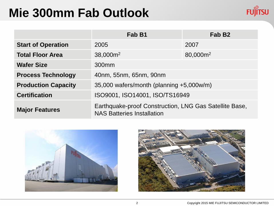
Mie 300mm Fab Outlook
Fab B1 Fab B2
Start of Operation 2005 2007
Total Floor Area 38,000m2 80,000m2
Wafer Size 300mm
Process Technology 40nm, 55nm, 65nm, 90nm
Production Capacity 35,000 wafers/month (planning +5,000w/m)
Certification ISO9001, ISO14001, ISO/TS16949
Major Features Earthquake-proof Construction, LNG Gas Satellite Base,
NAS Batteries Installation
Copyright 2015 MIE FUJITSU SEMICONDUCTOR LIMITED 2
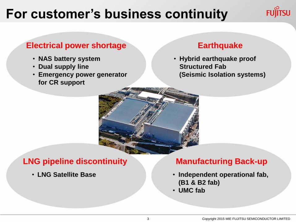
For customer’s business continuity
Copyright 2015 MIE FUJITSU SEMICONDUCTOR LIMITED 3
Manufacturing Back-up
• Independent operational fab,
(B1 & B2 fab)
• UMC fab
Electrical power shortage
• NAS battery system
• Dual supply line
• Emergency power generator
for CR support
LNG pipeline discontinuity
• LNG Satellite Base
Earthquake
• Hybrid earthquake proof
Structured Fab
(Seismic Isolation systems)
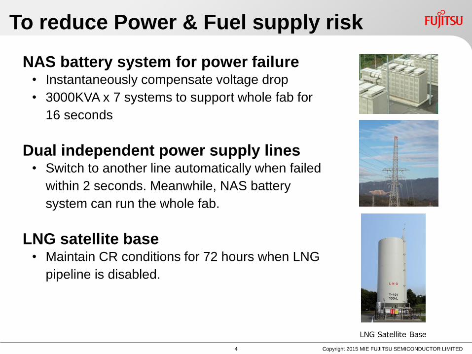
NAS battery system for power failure • Instantaneously compensate voltage drop
• 3000KVA x 7 systems to support whole fab for
16 seconds
Dual independent power supply lines • Switch to another line automatically when failed
within 2 seconds. Meanwhile, NAS battery
system can run the whole fab.
LNG satellite base • Maintain CR conditions for 72 hours when LNG
pipeline is disabled.
To reduce Power & Fuel supply risk
Copyright 2015 MIE FUJITSU SEMICONDUCTOR LIMITED 4

Effect of Seismic Isolation systems
5
4
3
2
1
0
Acceleration (gal)
Flo
or
Le
ve
l
with Seismic Isolation
w/o Seismic Isolation
500 1000 1500 2000
Acceleration of 500 gal at ground level can be reduced by
Max.90%
Laminated Rubber Supports
Solid Sliding Supports
Oil Damper
Copyright 2015 MIE FUJITSU SEMICONDUCTOR LIMITED 5

UMC and MIFS Partnership
Since 2011
Fujitsu Semiconductor (FSL) has
outsourced its 65nm products to UMC
since 2011.
August, 2014
UMC and FSL entered into “Joint Venture
Agreement” and “40nm Technology
Transfer and License Agreement”.
December, 2014
Mie Fujitsu Semiconductor (MIFS) was
established as 100% subsidiary of FSL
and succeeded the 40nm license
agreement from FSL.
March, 2015
UMC become 9.3% shareholder of MIFS.
Current Structure (June, 2015)
UMC
MIFS
90.7% 9.3%
FSL
Fujitsu
100%
Copyright 2015 MIE FUJITSU SEMICONDUCTOR LIMITED 6
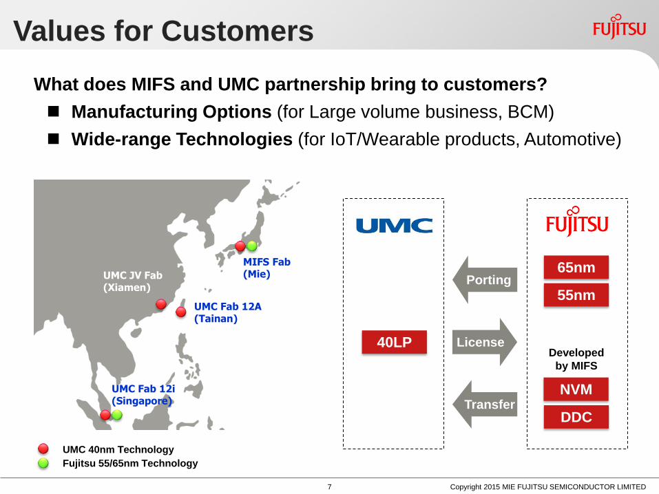
Values for Customers
What does MIFS and UMC partnership bring to customers?
Manufacturing Options (for Large volume business, BCM)
Wide-range Technologies (for IoT/Wearable products, Automotive)
UMC Fab 12A (Tainan)
UMC Fab 12i (Singapore)
UMC JV Fab (Xiamen)
MIFS Fab (Mie)
License
Porting
Transfer
40LP
NVM
55nm
65nm
DDC
Developed
by MIFS
UMC 40nm Technology
Fujitsu 55/65nm Technology
Copyright 2015 MIE FUJITSU SEMICONDUCTOR LIMITED 7

Mie Technology Line-up
5/15v HV
5/(8)v LDMOS
eNVM
Std. Flash
Plug-In
MTP/OTP
RF
Logic
HP LP HP LP LP DDC LP ULP DDC
90nm 65nm 55nm 40nm
Production Developing
Copyright 2015 MIE FUJITSU SEMICONDUCTOR LIMITED 8
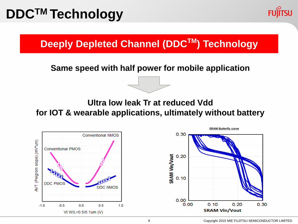
SRAM Butterfly curve
Same speed with half power for mobile application
Ultra low leak Tr at reduced Vdd
for IOT & wearable applications, ultimately without battery
DDCTM Technology
Deeply Depleted Channel (DDCTM) Technology
Copyright 2015 MIE FUJITSU SEMICONDUCTOR LIMITED 9

NVM for IOT & wearable applications
Conventional
Flash Memory
Plug-In Flash
MTP
• Can be plugged into
standard CMOS logic
process
• No need of IP redesign
• Complete NOR function
• Faster programming
speed and more flexible
than OTP and MTP
• Low process cost with
less mask layers
New Embedded NVM = Plug-In Flash Technology
Copyright 2015 MIE FUJITSU SEMICONDUCTOR LIMITED 10

Customer Satisfaction
Body
Cluster
Power train/ Chassis
Motor control
Functional safety
Automotive network
Infotainment
Graphics
Automotive network MCU
Graphics
mm wave radar
Security chip
Automotive network
Automotive network
(CAN,LIN)
MCU
Battery control
Stepper motor control
Graphics
MCU
High Quality
High Reliability
Mie Products for Automotive
Safety/Security
Copyright 2015 MIE FUJITSU SEMICONDUCTOR LIMITED 11
Wide Temperature & Voltage
High Safety
Copyright 2015 MIE FUJITSU SEMICONDUCTOR LIMITED 12
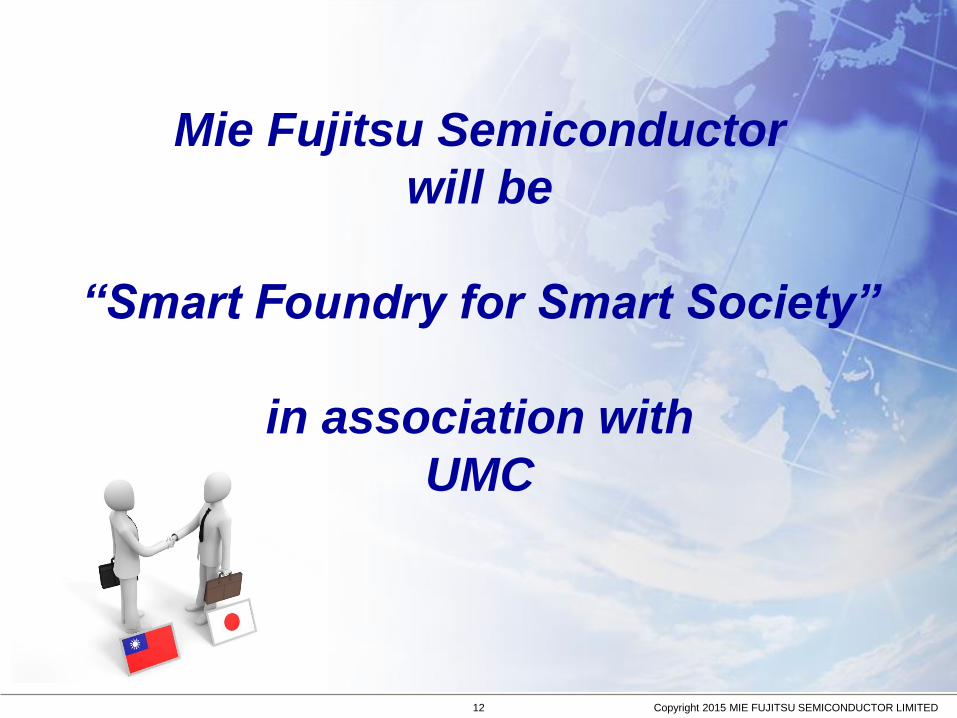
Mie Fujitsu Semiconductor
will be
“Smart Foundry for Smart Society”
in association with
UMC
Copyright 2010 FUJITSU LIMITED


![Bunrin Do - Famous Airplanes of the World 90 - Nakajima G5N & G8N [PF42]](https://static.fdocuments.in/doc/165x107/55cf96cd550346d0338de37e/bunrin-do-famous-airplanes-of-the-world-90-nakajima-g5n-g8n-pf42.jpg)