Part I 1.2 Signed Integer Representation Hardware and ...1.3 Character Representation ASCII (7 or 8...
12
Reference Sheet for C113 Architecture Spring 2017 Part I Hardware and Representation 1 Integers and Characters 1.1 Unsigned Integer Representation For a number d n d n-1 ...d 0 in base b we have ∑ n k=0 d k × b k . Hence n bits can represent 2 n - 1 unsigned integers. Converting from Decimal to Binary 1. Divide the number by 2, writing down the quotient and remainder. 2. Repeat this process on the quotient until 0 is reached. 3. The binary number is obtained by reading the remainders from bottom to top. Converting between Binary and Octal Simply convert from the least sig- nificant bit: 000 (0), 001 (1), 010 (2), 011 (3), 100 (4), 101 (5), 110 (6), 111 (7). Converting between Binary and Hexadecimal Simply convert from the least significant bit: 0000 (0), 0001 (1), 0010 (2), 0011 (3), 0100 (4), 0101 (5), 0110 (6), 0111 (7), 1000 (8), 1001 (9), 1010 (A), 1011 (B), 1100 (C), 1101 (D), 1110 (E), 1111 (F). Radix Arithmetic Exactly as for decimal but use the base (2 for binary) as point of reference instead of 10. Bit Groups Bit (1), Byte (8), Word (usually 16, 32 or 64). 1.2 Signed Integer Representation Sign and Magnitude 0 for positive, 1 for negative, followed by value. Has several disadvantages: 1. Two bit patterns for 0, which wastes a value and requires hardware to treat both values as 0. 2. Explicitly need to implement substractors and adders, so more costly to implement. One’s Complement Invert each bit for negative. Still two bit patterns for 0, which means result after operation not always correct. Two’s complement Complement each bit and add 1 to result. 1. -X defined as 2 n - X 2. X + ¯ X =1 ... 111 2 = -1 ⇐⇒ -X = ¯ X +1 3. n bits can represent any integer in the range from -2 n-1 to 2 n-1 - 1. Excess n Represent X as X + n Binary Coded Decimal Each nibble (4 bits) encodes value from 0 - 9. Sign nibble at end (1100 for + or 1101 for -). Arithmetic 1. Addition : Add and discard carry bit. 2. Subtraction : Negate subtrahend, add as before. 3. Overflow : For two numbers which are both positive or both negative, over- flow occurs iff the result has opposite sign. 1
Transcript of Part I 1.2 Signed Integer Representation Hardware and ...1.3 Character Representation ASCII (7 or 8...

Reference Sheet for C113 Architecture
Spring 2017
Part I
Hardware and Representation
1 Integers and Characters
1.1 Unsigned Integer Representation
For a number dndn−1 . . . d0 in base b we have∑n
k=0 dk × bk.Hence n bits can represent 2n − 1 unsigned integers.
Converting from Decimal to Binary
1. Divide the number by 2, writing down the quotient and remainder.
2. Repeat this process on the quotient until 0 is reached.
3. The binary number is obtained by reading the remainders from bottom totop.
Converting between Binary and Octal Simply convert from the least sig-nificant bit:000 (0), 001 (1), 010 (2), 011 (3), 100 (4), 101 (5), 110 (6), 111 (7).
Converting between Binary and Hexadecimal Simply convert from theleast significant bit:0000 (0), 0001 (1), 0010 (2), 0011 (3), 0100 (4), 0101 (5), 0110 (6), 0111 (7), 1000(8), 1001 (9), 1010 (A), 1011 (B), 1100 (C), 1101 (D), 1110 (E), 1111 (F).
Radix Arithmetic Exactly as for decimal but use the base (2 for binary) aspoint of reference instead of 10.
Bit Groups Bit (1), Byte (8), Word (usually 16, 32 or 64).
1.2 Signed Integer Representation
Sign and Magnitude 0 for positive, 1 for negative, followed by value. Hasseveral disadvantages:
1. Two bit patterns for 0, which wastes a value and requires hardware to treatboth values as 0.
2. Explicitly need to implement substractors and adders, so more costly toimplement.
One’s Complement Invert each bit for negative. Still two bit patterns for 0,which means result after operation not always correct.
Two’s complement Complement each bit and add 1 to result.
1. −X defined as 2n −X
2. X + X̄ = 1 . . . 1112 = −1 ⇐⇒ −X = X̄ + 1
3. n bits can represent any integer in the range from −2n−1 to 2n−1 − 1.
Excess n Represent X as X + n
Binary Coded Decimal Each nibble (4 bits) encodes value from 0 - 9. Signnibble at end (1100 for + or 1101 for -).
Arithmetic
1. Addition: Add and discard carry bit.
2. Subtraction: Negate subtrahend, add as before.
3. Overflow : For two numbers which are both positive or both negative, over-flow occurs iff the result has opposite sign.
1
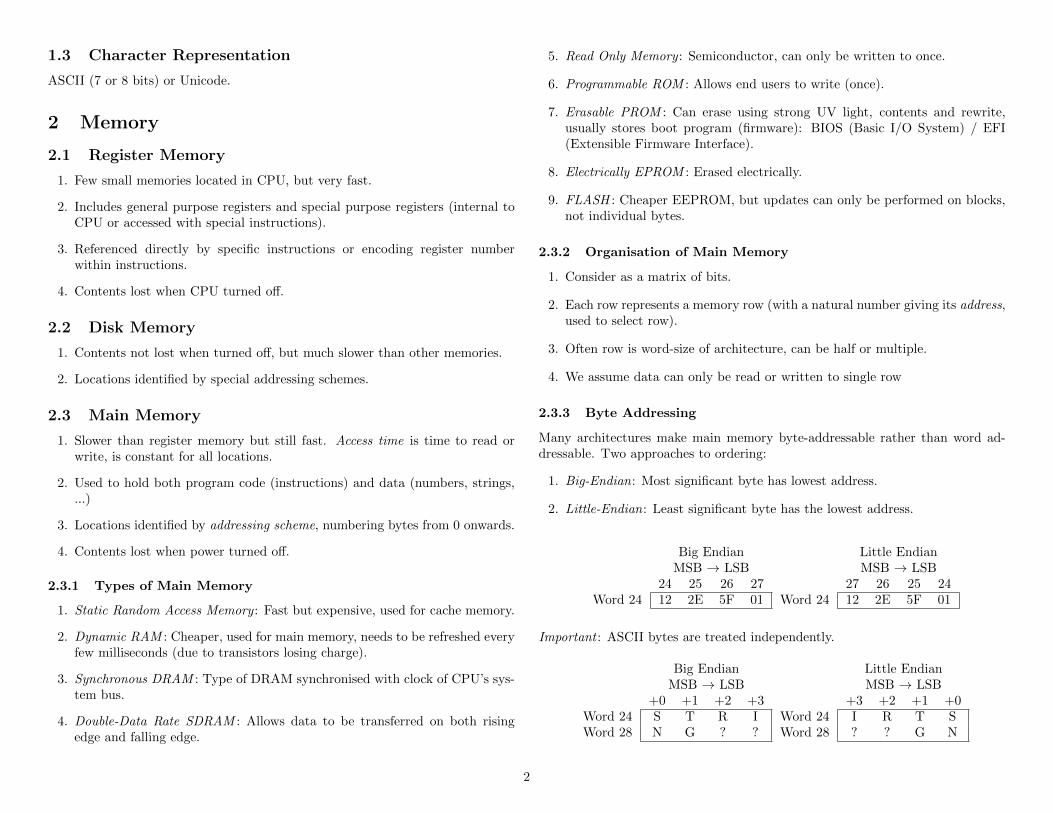
1.3 Character Representation
ASCII (7 or 8 bits) or Unicode.
2 Memory
2.1 Register Memory
1. Few small memories located in CPU, but very fast.
2. Includes general purpose registers and special purpose registers (internal toCPU or accessed with special instructions).
3. Referenced directly by specific instructions or encoding register numberwithin instructions.
4. Contents lost when CPU turned off.
2.2 Disk Memory
1. Contents not lost when turned off, but much slower than other memories.
2. Locations identified by special addressing schemes.
2.3 Main Memory
1. Slower than register memory but still fast. Access time is time to read orwrite, is constant for all locations.
2. Used to hold both program code (instructions) and data (numbers, strings,...)
3. Locations identified by addressing scheme, numbering bytes from 0 onwards.
4. Contents lost when power turned off.
2.3.1 Types of Main Memory
1. Static Random Access Memory : Fast but expensive, used for cache memory.
2. Dynamic RAM : Cheaper, used for main memory, needs to be refreshed everyfew milliseconds (due to transistors losing charge).
3. Synchronous DRAM : Type of DRAM synchronised with clock of CPU’s sys-tem bus.
4. Double-Data Rate SDRAM : Allows data to be transferred on both risingedge and falling edge.
5. Read Only Memory : Semiconductor, can only be written to once.
6. Programmable ROM : Allows end users to write (once).
7. Erasable PROM : Can erase using strong UV light, contents and rewrite,usually stores boot program (firmware): BIOS (Basic I/O System) / EFI(Extensible Firmware Interface).
8. Electrically EPROM : Erased electrically.
9. FLASH : Cheaper EEPROM, but updates can only be performed on blocks,not individual bytes.
2.3.2 Organisation of Main Memory
1. Consider as a matrix of bits.
2. Each row represents a memory row (with a natural number giving its address,used to select row).
3. Often row is word-size of architecture, can be half or multiple.
4. We assume data can only be read or written to single row
2.3.3 Byte Addressing
Many architectures make main memory byte-addressable rather than word ad-dressable. Two approaches to ordering:
1. Big-Endian: Most significant byte has lowest address.
2. Little-Endian: Least significant byte has the lowest address.
Big Endian Little EndianMSB → LSB MSB → LSB
24 25 26 27 27 26 25 24Word 24 12 2E 5F 01 Word 24 12 2E 5F 01
Important : ASCII bytes are treated independently.
Big Endian Little EndianMSB → LSB MSB → LSB
+0 +1 +2 +3 +3 +2 +1 +0Word 24 S T R I Word 24 I R T SWord 28 N G ? ? Word 28 ? ? G N
2

2.3.4 Word Allignment
1. Some architectures allow any word-sized bit group regardless of byte address.
2. Aligned access: acess begins on memory word boundary.
3. Unaligned access: does not. Slow because requires reading of required bitsfrom adjacent words and concatenating together.
2.3.5 Modules and Chips
1. RAM comes physcially in modules, each comprised of several chips.
2. DIMMs (dual inline memory modules) support 64-bit transfers, SIMMs sup-port 32-bit.
3. A chip with length 2k requires k address bits.
4. Number of chips = size of memory / size of chip.
5. Chips per module = width of memory word / width of chip.
6. Number of modules = number of chips / chips per module.
E.g. 1M×16 bit main memory made of 256K×4 bit chips has 16 chips, 4 chipsper module, 4 modules.
2.3.6 Interleaved Memory
Some address bits select module, and remaining bits select row.
1. Low-order interleaved memory : Module selection bits are least significantbits in memory address.
2. High-order interleaved : Module selection bits are most significant bits.
3. If more than one module can be read/written at a time:
(a) Low-order: Read same row in each module. E.g. single multi-wordaccess of sequential data.
(b) High-order: Different modules independently accessed by different units.E.g. CPU can access rows in one module, hard disk / another CPUaccess row in another module concurrently.
3 The CPU
1. Consider the task A = B + C. We compile this into a sequence of assemblyinstructions: LOAD R2 B. ADD R2, C. STORE R2, A. (where A, B, Cdesignate memory locations)
2. Consider also an architecture with 16-bit words, 4 general purpose registers(R0, R1, R2, R3), 16 different instructions in its instruction set, representsintegers using two’s complement.
3. Consider finally an instruction format with: 4 bits for OPCODE (identifiesCPU operation), 2 bits for REG (defines a general purpose register), 10 bitsfor ADDRESS (defines address of word in RAM).
Von Neumann Machine Model
1. 3 subsystems: CPU, main memory, I/O system.
2. Main memory holds program as well as data.
3. Instructions are executed sequentially.
4. Single path exists between control unit and main memory, leads to von Neu-mann bottleneck.
3.1 CPU Organisation
1. PC : Holds address of next instruction to be fetched from memory.
2. IR: Holds each instrcution after being fetched.
3

3. Instruction Decoder : Decodes (splits) contents of IR for control unit to in-terpret.
4. Control unit : Co-ordinates activity in CPU. Connected to all parts of CPU,includes timing circuit.
5. ALU : Carries out arithmetic and logical operations.
(a) ALU Input Registers 1 & 2 : Holds operands for ALU.
(b) ALU Output register : Holds result of ALU operation. Result is thencopied to final destination (e.g. CPU register, main memory, I/O de-vice).
6. General-Purpose Registers: For use by programmer.
7. Buses: Pass information within CPU and between CPU and main memory.Generally transfer >1 bit at a time.
(a) Address Bus: sends address from CPU to main memory, indicates ad-dress in memory to read/write to.
(b) Data Bus: bidirectional, sends a word from CPU to main memory orvice versa.
(c) Control bus: indicates whether CPU is reading or writing, i.e. directionof data bus.
3.2 The Fetch-Execute Cycle
1. Fetch Instruction and Increment Program Counter. Eg.:
(a) Address goes from PC to address bus.
(b) Control bus set to 0.
(c) Address goes from address bus to memory.
(d) 0 goes from control bus to memory (so READ).
(e) PC incremented.
(f) Instruction goes from memory[address] to data bus.
(g) Instruction goes from data bus to IR.
2. Decode Instruction. E.g.:
(a) Instruction goes from IR to instruction decoder.
(b) OPCODE, REG and ADDRESS go from decoder to control unit.
3. Execute Instruction (Fetch Operands, Perform Operation, Store Results).E.g. LOAD:
(a) ADDRESS goes from control unit to address bus.
(b) Control bus set to 0.
(c) ADDRESS goes from address bus to memory.
(d) 0 goes from control bus to memory (so READ).
(e) Value goes from Memory[ADDRESS] to data bus.
(f) Value goes from data bus to REG.
4. E.g. ADD:
(a) Value 1 goes from REG to ALU input reg 1.
(b) ADDRESS goes from control unit to address bus.
(c) Control bus set to 0.
(d) ADDRESS goes from address bus to memory.
(e) 0 goes from control bus to memory (so READ).
(f) Value 2 goes from memory[ADDRESS] to data bus.
(g) Value 2 goes from data bus to ALU reg 2.
(h) Operation goes from control unit to ALU (so ADD).
(i) Final value goes from ALU output reg to REG.
5. E.g. WRITE:
(a) Value goes from REG to data bus.
(b) ADDRESS goes from control unit to address bus.
(c) Control bus set to 1.
(d) Value goes from data bus to memory.
(e) ADDRESS goes from address bus to memory.
(f) 1 goes from control bus to memory (so WRITE).
6. Repeat Forever
4
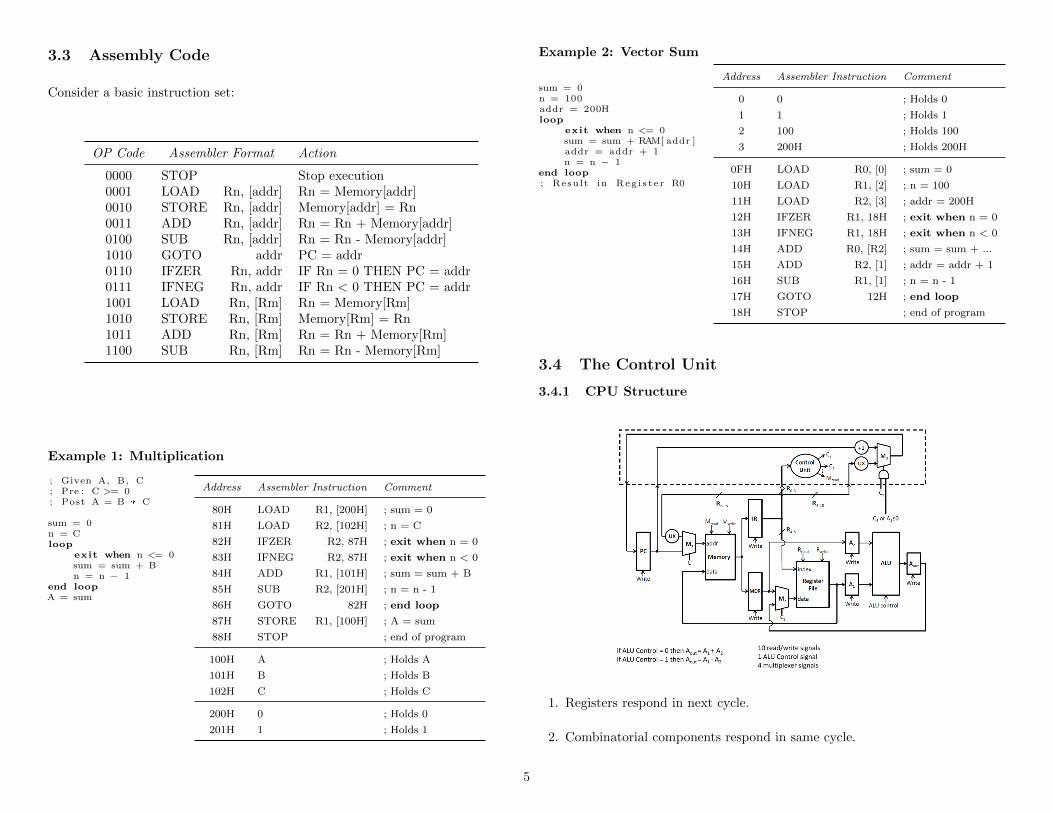
3.3 Assembly Code
Consider a basic instruction set:
OP Code Assembler Format Action
0000 STOP Stop execution0001 LOAD Rn, [addr] Rn = Memory[addr]0010 STORE Rn, [addr] Memory[addr] = Rn0011 ADD Rn, [addr] Rn = Rn + Memory[addr]0100 SUB Rn, [addr] Rn = Rn - Memory[addr]1010 GOTO addr PC = addr0110 IFZER Rn, addr IF Rn = 0 THEN PC = addr0111 IFNEG Rn, addr IF Rn < 0 THEN PC = addr1001 LOAD Rn, [Rm] Rn = Memory[Rm]1010 STORE Rn, [Rm] Memory[Rm] = Rn1011 ADD Rn, [Rm] Rn = Rn + Memory[Rm]1100 SUB Rn, [Rm] Rn = Rn - Memory[Rm]
Example 1: Multiplication
; Given A, B, C; Pre : C >= 0; Post A = B * C
sum = 0n = Cloop
exit when n <= 0sum = sum + Bn = n − 1
end loopA = sum
Address Assembler Instruction Comment
80H LOAD R1, [200H] ; sum = 0
81H LOAD R2, [102H] ; n = C
82H IFZER R2, 87H ; exit when n = 0
83H IFNEG R2, 87H ; exit when n < 0
84H ADD R1, [101H] ; sum = sum + B
85H SUB R2, [201H] ; n = n - 1
86H GOTO 82H ; end loop
87H STORE R1, [100H] ; A = sum
88H STOP ; end of program
100H A ; Holds A
101H B ; Holds B
102H C ; Holds C
200H 0 ; Holds 0
201H 1 ; Holds 1
Example 2: Vector Sum
sum = 0n = 100addr = 200Hloop
exit when n <= 0sum = sum + RAM[ addr ]addr = addr + 1n = n − 1
end loop; Result in Reg i s t e r R0
Address Assembler Instruction Comment
0 0 ; Holds 0
1 1 ; Holds 1
2 100 ; Holds 100
3 200H ; Holds 200H
0FH LOAD R0, [0] ; sum = 0
10H LOAD R1, [2] ; n = 100
11H LOAD R2, [3] ; addr = 200H
12H IFZER R1, 18H ; exit when n = 0
13H IFNEG R1, 18H ; exit when n < 0
14H ADD R0, [R2] ; sum = sum + ...
15H ADD R2, [1] ; addr = addr + 1
16H SUB R1, [1] ; n = n - 1
17H GOTO 12H ; end loop
18H STOP ; end of program
3.4 The Control Unit
3.4.1 CPU Structure
1. Registers respond in next cycle.
2. Combinatorial components respond in same cycle.
5

3.4.2 Micro-Steps
1. Required Inputs: One of 16 opcodes (4 bits), one of 8 states (3 bits).
2. Required Outputs: 15 control signals (see circuit diagram), next state (3 bits).
ROM Implementation 7 bits input, 18 bits output so size is 27 × 18.
Microsequencer Implementation
1. Micro-program counter used to keep track of current state.
2. Multiplexer chooses: 0 - next instruction, 1 - choose based on opcode, 2 -increment by one.
3. Instruction Decode ROM : 4 inputs, 3 outputs so size 24 × 3.
4. Control Logic ROM : 3 inputs, 17 outputs so size 23 × 17.
Part II
Intel 64 Architecture
4 Intel 64 Introduction
4.1 Memory
4.1.1 Registers
Register 64-bit 32-bit 16-bit 8-bit (high) 8-bit (low)
A rax eax ax ah al
B rbx ebx bx bh bl
C rcx ecx cx ch cl
D rdx edx dx dh dl
Source Index rsi esi si sil
Destination Index rdi edi di dil
Stack Pointer rsp esp sp spl
Base Pointer rbp ebp bp bpl
Instruction Pointer rip
Flags rflags
Instruction Pointer Register
� Holds address of next instruction to be executed.
� Rarely manipulated directly by programs.
6

� Used implicitly by instructions such as call, jmp and ret.
� Used to implement if and while statements, method calls.
Flags Register
� 6: Zero flag, 1 if result is 0.
� 7: Sign flag: Most signifcant bit of result (sign bit for signed int).
� 11: Overflow flag: 1 if signed result overflows.
� 0: Carry flag: 1 if unsigned result overflows.
� 2: Parity flag: 1 if LS byte of result contains even number of bits.
4.1.2 Main Memory
Byte addresable, little endian, non-aligned access is allowed.
4.2 Instructions
Generally have the form label: opcode Destination, Source ; comments.
Global Variables Examples:
age dw 21 ; word with val 21
total dd 999 ; doubleword with val 999
message db "hello" ; 5-byte string hello
sequence dw 1,2,3 ; 3 words with vals 1,2,3
array times 100 dw 33 ; 100 words with val 33
little resw 100 ; reserve 100 words
big resd 1000 ; reserve 1000 dwords
dozen equ 12 ; defines constant ‘dozen ’
5 Addressing Modes
Example assembly instructions:
mov rax , [rpb+4] ; rax = memory[rpb + 4]
add ax, [bx] ; ax = ax + memory16[bx]
sub rax , 45 ; rax = rax - 45
Register Operands E.g. rax, eax, dx, al, si, bp.Operand is value of specified register. Note dest and src operands usually needto be same size.
Immediate Operands E.g. 23, 67H, 101010B, ‘A’Operand is the constant value specified directly. Not normally applicable for destoperands.
Memory Operands [BaseReg + Scale * IndexReg + Disp] where:
1. BaseReg can be any register
2. Scale ∈ {1, 2, 4, 8}
3. IndexReg can be any register except rsp
4. Disp is a 64-bit constant
Note that order is unimportant. Size of operands normally inferred.
1. [Disp]: Direct addressing : address given by constant value. Allows accessto global variables.
2. [BaseReg]: Register indirect : address given by contents of register. Dynam-ically points to variables in memory based on computed addresses.
3. [BaseReg + Disp]: Register Relative: Sum gives address. Disp can be neg-ative. Can be used to access object fields, array elements.
4. [BaseReg + IndexReg]: Based-Indexed : Can be used to access array ele-ments, where start of array dynamically determined.
5. [BaseReg + IndexReg + Disp]: Based Relative Index : Can be used to ac-cess arrays of objects, arrays within objects, arrays on stack.
6. [Scale * IndexReg + Disp]: Scaled-Indexed : Efficient access to array ele-ments when element size is 1, 2, 4 or 8 bytes.
7. [BaseReg + Scale * IndexReg + Disp]: Efficient access to array elementswithin objects / on the stack.
7

6 Programming
6.1 Arithmetic Instructions
Instruction Operation Description
add dst, src dst = dst + src Addsub dst, src dst = dst - src Subtractcmp dst, src dst - src Compare and set RFLAGSinc opr opr = opr + 1 Increment by 1dec opr opr = opr - 1 Decrement by 1neg opr opr = - opr Negateimul dst, src dst = dst * src Integer multiplyimul dst, src, imm dst = src * imm Integer multiply
idiv opr*al = ax div opr
Integer divideah = ax mod opr
idiv opr*ax = (dx:ax) div opr
Integer dividedx = (dx:ax) mod opr
sal dst, n dst = dst * 2n Shift arithmetic leftsar dst, n dst div dst * 2n Shit arithmetic rightcbw ax = al Convert byte to wordcwde eax = ax Convert word to doublewdcdq edx:eax = eax Conver double to quadwdcqo rdx:rax = rax Extend quadword
* Must be register or memory only. idiv works similarly in 32 and 64 bits (usingextended registers).
Overflows
1. E.g. occurs on signed byte additions where A+B > 127 or A+B < −128.
2. Sets overflow flag in RFLAGS.
3. We can use jo ov label ; Jump to ov label if overflow.
Division by Zero Check the zero flag:
cmp bh , 0 ; compare divisor with 0
je zd_label ; jump to zd_label if divisor is zero
idiv bh ; otherwise go ahead with division
6.2 Logical Instructions
Instruction Operation Description
and dst, src dst = dst & src Bitwise andtest dst, src dst & src Bitwise and, set RFLAGSor dst, src dst = dst | src Bitwise orxor dst, src dst = dst ˆ src Bitwise xornot opr opr = ˜ opr Bitwise not
1. and clears specific (0 in src) bits in dst.
2. or sets specific (1 in src) bits in dst.
3. xor toggles specific (1 in src) bits in dst.
Boolean Expressions Represent boolean using a full byte: 0 for false, trueotherwise.
6.3 Jump Instructions
Instruction Flag Condition Description
jmp label None Jumpje/jz label ZF = 1 Jump if zero (equal)jne/jnz label ZF = 0 Jump if not zero (not equal)jg label ZF = 0 and SF = 0 Jump if greater thanjge label SF = 0 Jump if greater than or equal tojl label SF = 1 Jump if less thanjle label ZF = 1 or SF = 1 Jump if less than or equal to
If-then-else if (age < 100) then s1 else s2:
if: cmp word[age], 100
jge else
; s1
jmp endif
else: ; s2
endif:
While loop while (age < 100) s:
8

while: cmp word[age], 100
jge endwhile
; s
jmp while
endwhile:
For loop for (age = 1; age < 100; age++) s:
for: mov word[age], 1
next: cmp word[age], 100
jge endfor
; s
inc word[age]
jmp next
endfor:
6.4 Methods
1. Jump to the beginning of some code, execute it, return (possibly with results)to where called from.
2. Need to consider: parameters, local variable, nested and recursive methodcalls.
6.4.1 Stacks
1. Last-in, first-out: two basic operations, push and pop.
2. rsp (stack pointer) points to top of stack.
3. rbp (base pointer) keeps track of data on the stack.
NB: Stack grows downwards, from higher addresses to lower addresses.
Instruction Operation Description
push word opr*rsp = rsp - 2
Push word onto stackmemory[rsp] = word opr
pop word opr*word opr = memory[rsp]
Pop word off of stackrsp = rsp + 2
pushfqZF = 0
Push RFLAGS onto stackZF = 0 and SF = 0
popfqSF = 0
Pop RFLAGS off stackSF = 1
call methodpush rip Push return address andjmp method jump to method code
ret pop ripPop return address intorip (so jumping back)
* Quadwords can also be pushed and popped. No other operand sizes are allowed.
6.4.2 Calling Convention
Calling method (Caller) Called method (Callee)
1. Push parameters, last to first.2. Push object instance.3. Jump to (call) method.4. Save registers on stack.5. Execute body of method.6. Copy result to eax or rax.7. Restore registers from stack.8. Jump back (return) from method.9. Remove object instance from stack.10. Remove parameters from stack.11. Use method result.
Local Variables Callee makes space for local variables:
push rbp ; push caller ’s frame pointer onto stack
mov rbp , rsp ; set frame pointer to current stack pointer
sub rsp , nbytes ; allocate nbytes for local vars
and then de-allocates these variables:
mov rsp , rbp ; restore stack pointer
pop rbp ; restore caller ’s frame pointer
9

Array and object parameters We push the start address rather than itsvalue. We can use lea (load effective address) to do this: lea dstreg, [BaseReg
+ Scale * IndexReg + Disp].
Object Method Calls Need to be translated as if they were written withouta class.
Example: Caller
coord point...point.setpos(3, 5)
/* translated to: */coord_setpos(point , 3, 5)
point resd 2 ; allocate point...push qword 5 ; push 5push qword 3 ; push 3push qword point ; push @pointcall coord_setpos ; call calleeadd rsp , 24 ; restore stack pointer
Example: Callee
class coord {int row;int col;void setpos (int x, int y) {
row = x;col = y;
}}
/* translated to: */void coord_setpos (coord this ,
int x, int y) {this.row = x;this.col = y;
}
coord_setpos:push rbp ; save frame pointermov rbp , rsp ; setup frame pointerpush rsi ; save rsimov rsi , [rbp +16] ; rsi = this
mov rax , [rbp +24] ; rax = xmov [rsi], rax ; this.row = xmov rax , [rbp +32] ; rax = ymov [rsi+4], rax ; this.col = y
pop rsi ; restore rsipop rbp ; restore frame pointerret ; return
7 Floating Point Numbers
Represent numbers in format M × 2E .
� M is the coefficient, significand, fraction or mantissa. No. of bits determinseprecision.
� E is the exponent or characteristic. No. of bits determines range.
� 2 is the radix or base.
Zones of Expressibility E.g. with signed 3-digit coefficient and signed 2-digitexponent:
Floating Point vs Real Numbers
1. Floating points have a finite range and a finite number of values.
2. The gap between numbers varies.
3. Incorrect results are possible.
Normalised Form We normalise coefficients in the range [1, . . . R) where R isthe base.
Binary Fractions E.g. decimal value of 0.01101?
32 16 8 4 2 1. 0 1 1 0 1
= 8+4+132 = 13
32
E.g. binary value of 0.6875?
=1.375
2=
1
2+
0.75
4=
1
2+
1.5
8=
1
2+
1
8+
1
16= 0.1011
Multiplication Multiply coefficents, add exponents, normalise result.
Addition Need to align smaller exponent, by shifting its coefficient the corre-sponding number of digits to the right.
10
Comparing Due to potential for inexact results, a = b should be adjusted tob− ε < a < b+ ε. Or calculated closeness based on relative sizes.
Truncation and Rounding If result is too large to store in coefficent truncate(biased error) or round (unbiased).
Exponent Overflow and Underflow Set value as infinity / zero or raise anexception.
7.1 IEEE Floating Point Standard
Sign S Exponent E Significand F1 bit 8 (11 ) bits 23 (52 ) bits
Single Precision
1. Represented value is ±1.F × 2E−127.
2. First significand bit (1) is hidden.
3. Note that exponents stored in excess-127 values.
Double Precision Value is ±1.F × 2E−1023.
Conversion to IEEE Format E.g. 42.6875 in single precision format.
1. Convert to binary number: 10 1010.1011
2. Normalise : 1.0101 0101 1×25
3. Significand field: 0101 0101 1000 0000 0000 000
4. Exponent field: 5 + 127 = 132 = 1000 0100
GivesS E F0 1000 0100 0101 0101 1000 0000 0000 000
or 422A C000.
Conversion from IEEE Format E.g. BEC0 0000 or 1 0111110110000000000000000000000 from single precision format.
1. Exponent field: 125 - 127 = - 2
2. Significand field: 1.1
3. Add sign bit: - 1.1×2−2 = - 0.25 - 0.125 = - 0.375
Addition
1. Shift smaller number to the right so that exponents are the same.
2. Sum significands.
Special Values
1. Zero has 0 exponent and 0 significand.
2. Denormalised numbers (0.F × 2−126) have 0 exponent.
3. Infinity has 255 exponent and 0 significand.
4. NaN has 255 exponent.
5. Normalised numbers have 1..254 exponent.
Infinity and NaN do what you expect under mathematical operations.
8 Input and Output
I/O Controllers
1. Provide CPU with a programming interface.
2. Data ports used for passing data to / from CPU.
3. Control ports used to issue I/O commands and check device status.
I/O Addressing I : Seperate Address Space
1. I/O ports have their own small address space. Architecture provides com-mands to access it.
2. Control bus signals if transfer is for I/O or main memory address space.
3. Intel 64 provides 64K 8-bit I/O ports.
in ax, 20 ; copy 16 bits from I/O port 20 to ax
out 35, al ; copy 8 bits from al to I/O port 35
I/O Addressing I : Memory Mapped I/O
1. I/O ports appear as normal memory locations.
2. Any instruction acting on memory operands can be used on I/O ports.
3. Intel 64 also supports this.
11

Four I/O Schemes
1. Programmed I/O : Continually polls a control port until it’s ready, then trans-fers.
(a) Pros: Simple to program and guarantees response times.
(b) Cons: Poor CPU utilisation, awkward to handle multiple devices.
2. Interrupt-driven I/O : Initiate transfer and then do something else, inter-rupt CPU when transfer is complete. Control then transferred to interrupthandler.
(a) Cons: Need to save and restore CPU state. Bad for high-speed high-data volume devices that might lose data if they are not serviced quicklyenough. Bad if devices continually require attention.
3. DMA I/O : Initiate large data block transfer. CPU writes start address ofblock, number of bytes, and direction of transfer to DMA’s I/O ports and is-sues start command. DMA controller transfers block of data to main memorywithout direct CPU intervention. Interrupts CPU when completed.
(a) Pro: Greatly reduces interrupts.
4. I/O processor : Delegate I/O tasks to dedicated processor. Much more pow-erful solution.
Operating Systems: Concurrency Interleaves processes. Operating systemis a scheduler that puts processes (threads) in different states (using interrupts).
8.1 Interrupts
Locating Interrupt Handler
1. Device that wishes to interrupt CPU sends an interrupt signal to the CPUalong with a interrupt vector number.
2. Interrupt vector number indexes interrupt descriptor table.
3. Start address of IDT is held in special CPU register called IDT base register.
Calling the Interrupt Handler The Intel 64 CPU:
1. Completes the executing instruction.
2. Pushes RFLAGS onto the stack.
3. Clears the interrupt flag bit in the RFLAGS register.
4. Push the CS register and return address
5. Jump to interrupt handler using IDT.
Handler executes iret which restores state of RFLAGS, CS and RIP and jumpsto return address on stack. Preserving registers is duty of handler.
Enabling and Disabling Interrupts
1. Interrupts automatically disabled on entering handler.
2. Interrupts can be re-enabled by setting IF (interrupt enable flag) with sti.
3. Interrupts can be disabled using cli.
Drivers
1. Devices controlled by reading/writing to I/O ports (memory locations inmemory-mapped I/O).
2. Completion of I/O request signalled by sending interrupt vector number whi-ich causes CPU to call device’s interrupt handler.
3. Top half (interrupt handler) services interrupt - check for errors and copiesdata to / from memory and shares it with bottom half.
4. Bottom half runs as a schedulable thread within the OS and interacts withthe device via I/O ports, the top half (via shared memory) and the user-levelprocess.
Types of Interrupt
1. External I/O Device-generated (vectors 32-255 ): I/O devices sends interruptvia buses. The only asynchronous type.
2. CPU-generated (0-18 ) : Attempt to execute illegal operation.
3. Software-generated: Generated by instruction.
Software Interrupts (System Calls / Traps)
1. syscall used to call operating system functions.
2. System call number held in rax. E.g. 0 = read from standard input, 1 =write to standard output.
3. Parameters held in rdi, rsi, rdx, rcx, r8, r9.
4. Result passed into rax.
12