PARAMETRIZATION VIA NFC - MobileKnowledge
41
PUBLIC JORDI JOFRE NFC READERS NFC EVERYWHERE 21/02/2017 WEBINAR SERIES: HOW TO BUILD NFC APPLICATIONS PARAMETRIZATION VIA NFC
Transcript of PARAMETRIZATION VIA NFC - MobileKnowledge
PUBLIC
JORDI JOFRENFC READERS
NFC EVERYWHERE21/02/2017
WEBINAR SERIES:
HOW TO BUILD NFC APPLICATIONS
PARAMETRIZATION VIA NFC

3
Parametrization via NFCAgenda
• NFC DIN rail module demo
− Demo functionality
− Hardware details
− How the NTAG I2C plus is used
− MCU / embedded software integration
− Phone / NFC device software integration
− Available resources
• Wrap up and Q&A

6
NFC DIN RAIL MODULE DEMO DEMO FUNCTIONALITY

7
NFC DIN rail module demoElements
• It demonstrates the use of NFC for:
1. Wireless parametrization & Zero power configuration
2. Product diagnosis
3. Wireless firmware update
NFC interface
Power switch
(220V)
Light bulbs
1 32
LCD

8
Wireless
parametrization with
DIN module powered
With a tap, settings are
saved in the DIN
module
Zero power operation
with the DIN module
powered off
When the DIN module is
powered, it loads the
stored configuration
Wireless parametrization & zero power configuration

9
Product diagnostics can
be retrieved even with the
DIN module powered off
With a tap, phone
displays the light bulb
switching counters value
Product diagnosis – Read switching counters

10
Product diagnostics can
be reset even with the
DIN module powered off
With a tap, phone resets
the light bulb switching
counters to zero
Product diagnosis – Reset switching counters

11
Keep the right button
pressed to enter in
“flash” mode
Wait until binary file
transfer is completed
After flashing the new
FW, light bulb blinking
frequency is now higher
Phone app lets us select
the new binary file to be
flashed
Wireless firmware upgrade

12
HARDWARE DETAILS

13
Disassembling NFC DIN rail module demo (I)
• Tearing down
Unmounting the
module from the DIN
rail
Unscrew and release
the power wires
Unscrew and release
light bulb power wires

14
Disassembling NFC DIN rail module demo (II)
Remove the module
from the DIN rail
Disassembling the
module

15
Hardware details - Transformer PCB
Electro mechanical relays
operating light bulbs
Transformer
(220 V AC to 12 V AC)
The transformer PCB includes:
• Three electromechanical relays controlling the light bulbs.
• Transformer converting 220 V to 12 V to supply the switching PCB.

16
Hardware details - Switching PCB
12 V AC (from
Transformer PCB)
Transistors controlling the signals to
be sent to the relays (12 V) in the
Transformer PCB
Signals coming from
the NTAG Explorer
board (LPC11U24 MCU)
The switching PCB contains:
• Power supply unit (AC/DC converter from 12V AC to
12V DC and 3V DC)
• Transistors controlling the input signal to be sent to the
relays in the Transfomer PCB
12 V DC
(supplying
transistors)
3 V DC
(supplying
Explorer board)

17
Hardware details - Explorer board + NTAG I2C plus flex antenna
• About the Explorer board HW:
− 5 buttons (3 Color buttons, RESET and ISP)
− NXP LM75B digital temperature sensor
− NXP LPC11U24 32-bit ARM Cortex-M0 microcontroller
− thermal watchdog
− RGB light
− LCD display
− microUSB for PC connection
− JTAG for FW upload
− I2C Bus Connector
• Class 6 flex antenna embedding NTAG I2C plus
* Design files for the Explorer board, Class 4 antenna and Class 6 flex antenna can be found in: http://www.nxp.com/products/wireless-connectivity/nfc-and-reader-ics/connected-tag-solutions/ntag-ic-plus-explorer-kit-development-kit:OM5569-NT322E?tab=Design_Tools_Tab

18
NTAG I2C plus Explorer demokit and variants
Demokits for NTAG I2C plus
* NTAG I2C plus Explorer demokit info and ordering details: http://www.nxp.com/products/identification-and-security/nfc-and-reader-ics/connected-tag-solutions/ntag-ic-iplus-i-explorer-kit:OM5569-NT322E
Orderable part number: OM5569-NT322E
12NC: 935307849699
URL: http://www.nxp.com/demoboard/OM5569-NT322E.html
Ordering details
Orderable part number: OM5569-NT322ER
12NC: 935307848699
URL: http://www.nxp.com/demoboard/OM5569-NT322ER.html
Ordering details
Orderable part number: OM5569-NT322F
12NC: 935307851699
URL: http://www.nxp.com/demoboard/OM5569-NT322F.html
Ordering details

19
HOW THE NTAG I2C PLUS IS USEDPRODUCT FEATURES

20
How NTAG I2C plus works
The NTAG I²C plus connects to the
microcontroller via the I²C serial bus interface
NFC-enabled mobile device connects to
the MCU via the NFC interface, using
the I²C as the communication conduit
Field Detection
Energy harvesting
SRAM memory
SRAM mirroring
Pass-through mode
Memory access management
Originality signature
Energy harvesting

21
Data exchange between I2C and NFC interfaces
Using the EEPROM in Passive or Static mode
• The NTAG I²C plus tag chip operates like a modem when in this
mode.
• Data flows from the NFC interface through an SRAM buffer to
the I²C serial bus interface or vice versa
• The on-chip, 64-byte SRAM preserves EEPROM access limits
Using the SRAM in pass-through mode
• With the power to the device off, the NFC interface can still operate
and write into the EEPROM.
• Later, when the device has power, the microprocessor can access
the previously written data via the I2C interface.
• Similarly, the microprocessor can write data to the EEPROM while
powered for later access via the NFC interface whether or not the
device has power.

22
HOW THE NTAG I2C PLUS IS USEDZERO POWER CONFIGURATION DEMO USE CASE

23
Application logic for zero power configuration use case (I)
Page
address
(HEX)
Byte number within a page
0 1 2 3
0x00
………
……
0x34
0x35
0x36
0x37
…… …
… …
0xF0
… ….
0xFB
0xFC
0xFD
0xFE
0xFF
Fig. Simplified NTAG I2C plus memory map
(NFC interface perspective)
EEPROM memory map
(NFC perspective)
Page address 0x34
Page address 0x35
Page address 0x35
Page address 0x35
Stores the Light bulb 1 setting (B1)
‘0’ – light bulb ON
‘1’ – light bulb OFF
‘2’ – light blink
Stores the Light bulb 3 setting (B3)
‘0’ – light bulb ON
‘1’ – light bulb OFF
‘2’ – light blink
Stores the Light bulb 2 setting (B2)
‘0’ – light bulb ON
‘1’ – light bulb OFF
‘2’ – light blink
Stores the language setting (L)
‘0’ – Deutsch
‘1’ – Bavarian
‘2’ – Swiss
‘3’ – English
‘4’ – French
SRAM mirror memory area (volatile memory)
EEPROM memory area (non-volatile memory)
I2C
LPCU1124
1. Phone
writes config
in EEPROM
0x34 B1
0x35 B2 B3 L

24
Application logic for zero power configuration use case (II)
SRAM mirror memory area (volatile memory)
EEPROM memory area (non-volatile memory)
3. MCU changes GPIO 17,
18 and 19 output config
according to B1, B2 and
B3 settings
3. MCU changes LCD
language message
according to L setting
Bonjour
4. Relays turn
ON / OFF light bulbs
4. The relay status changes
accordingly to GPIO
17,18,19 output value
2. MCU reads
config from
EEPROM
Page
address
(HEX)
Byte number within a page
0 1 2 3
0x00
………
……
0x34 B1
0x35 B2 B3 L
0x36
0x37
…… …
… …
0xF0
… ….
0xFB
0xFC
0xFD
0xFE
0xFF
Fig. Simplified NTAG I2C plus memory map
(NFC interface perspective)
I2C
LPCU1124
25
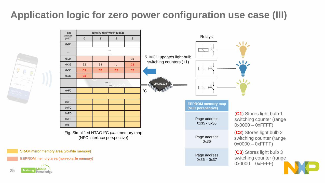
Application logic for zero power configuration use case (III)
SRAM mirror memory area (volatile memory)
EEPROM memory area (non-volatile memory)
Relays
5. MCU updates light bulb
switching counters (+1)
EEPROM memory map
(NFC perspective)
Page address
0x35 - 0x36
Page address
0x36
Page address
0x36 – 0x37
(C1) Stores light bulb 1
switching counter (range
0x0000 – 0xFFFF)
(C3) Stores light bulb 3
switching counter (range
0x0000 – 0xFFFF)
(C2) Stores light bulb 2
switching counter (range
0x0000 – 0xFFFF)
SRAM mirror memory area (volatile memory)
Page
address
(HEX)
Byte number within a page
0 1 2 3
0x00
………
……
0x34 B1
0x35 B2 B3 L C1
0x36 C1 C2 C2 C3
0x37 C3
…… …
… …
0xF0
… ….
0xFB
0xFC
0xFD
0xFE
0xFF
Fig. Simplified NTAG I2C plus memory map
(NFC interface perspective)
I2C
LPCU1124

26
HOW THE NTAG I2C PLUS IS USEDPRODUCT DIAGNOSIS DEMO USE CASE

27
Application logic for product diagnosis use caseRead diagnosis
Page
address
(HEX)
Byte number within a page
0 1 2 3
0x00
………
……
0x34 B1
0x35 B2 B3 L C1
0x36 C1 C2 C2 C3
0x37 C3
…… …
… …
0xF0
… ….
0xFB
0xFC
0xFD
0xFE
0xFF
Fig. Simplified NTAG I2C plus memory map
(NFC interface perspective)
SRAM mirror memory area (volatile memory)
EEPROM memory area (non-volatile memory)
I2C
LPCU1124
EEPROM memory map
(NFC perspective)
Page address
0x35 - 0x36
Page address
0x36
Page address
0x36 – 0x37
(C1) Stores light bulb 1
switching counter (range
0x0000 – 0xFFFF)
(C3) Stores light bulb 3
switching counter (range
0x0000 – 0xFFFF)
(C2) Stores light bulb 2
switching counter (range
0x0000 – 0xFFFF)
1. Phone reads switch
counters values from
EEPROM

28
Application logic for product diagnosis use caseReset diagnosis
EEPROM memory map
(NFC perspective)
Page address
0x35 - 0x36
Page address
0x36
Page address
0x36 – 0x37
(C1) Stores light bulb 1
switching counter (range
0x0000 – 0xFFFF)
(C3) Stores light bulb 3
switching counter (range
0x0000 – 0xFFFF)
(C2) Stores light bulb 2
switching counter (range
0x0000 – 0xFFFF)
SRAM mirror memory area (volatile memory)
EEPROM memory area (non-volatile memory)
1. Phone resets switch
counters to zero by
writing to EEPROM
Page
address
(HEX)
Byte number within a page
0 1 2 3
0x00
………
……
0x34 B1
0x35 B2 B3 L 0x00
0x36 0x00 0x00 0x00 0x00
0x37 0x00
…… …
… …
0xF0
… ….
0xFB
0xFC
0xFD
0xFE
0xFF
I2C
LPCU1124
Fig. Simplified NTAG I2C plus memory map
(NFC interface perspective)
0x35 B2 B3 L 0x00
0x36 0x00 0x00 0x00 0x00
0x37 0x00

29
HOW THE NTAG I2C PLUS IS USEDFIRMWARE UPGRADE DEMO USE CASE

30
Application logic for firmware upgrade use caseSecondary bootloader application
• NXP’s LPC11U24 microcontroller provides two methods to
update the flash contents:
− In-system-programming (ISP): This method is used when we flash
new contents using the USB port and a computer (drag-and-drop a
binary file).
− In application programming (IAP): Programming is performed by
erase and write operation on the on-chip flash memory, as directed by
the end-user application code
• A secondary bootloader application is a piece of code which
allows a user application code to be downloaded via alternative
channels to the USB (i.e.: firmware upgrade via NFC).
Sector Flash memory
Sector 0
MCU secondary
bootloader
application
Sector 1
Sector 2
Sector 3
Sector 4
DIN rail module
application demo
Sector 5
Sector 6
Sector 7
LPCU1124
IAP methods are used for firmware upgrade via NFC
The LPC11U24 flash memory is divided into 8
sectors of 4 Kb each one (total 32kB)
Fig. Simplified LPC11U24
flash memory map
31
Application logic for firmware upgrade use case
Page
address
(HEX)
Byte number within a page
0 1 2 3
0x00
………
……
0x34
0x35
0x36
0x37
…… …
… …
0xF0
Transmission of 64 byte data via
SRAM in pass-through mode
….
0xFC
0xFD
0xFE
0xFF
Sector Flash memory
Sector 0
MCU secondary
bootloader
application
Sector 1
Sector 2
Sector 3
Sector 4
Sector 5
Sector 6
Sector 7
I2C
LPCU1124
1. Phone uses SRAM to
transmit the binary file
in pieces of 64 bytes
Data flow direction (SRAM in pass through mode)
IAP
functions
SRAM mirror memory area (volatile memory)
EEPROM memory area (non-volatile memory)
Fig. Simplified LPC11U24
flash memory mapFig. Simplified NTAG I2C plus memory
map (NFC interface perspective)
Flash memory area
under upgrade
Firmware upgrade can be
performed with the DIN module
off using NTAG I2C plus
energy harvesting feature

32
SOFTWARE INTEGRATIONMCU / EMBEDDED

33
MCU code overview
LPCOpen software libraries (drivers and middleware) supporting development on top of LPC
MCU solutions. These two libraries bring support to LPC11U24 LPCXpresso board
Lpc_chip_11uxx_lib & nxp_lpcxpresso_11u24h_board_lib
Sample project that sets into blinking mode the NTAG I2C Explorer board LED as soon as an RF
field is detected.
NTAG_I2C_Explorer_Blink
* Reference MCU code can be downloaded from:
http://www.nxp.com/documents/software/SW3647.zip
Implements the NTAG I2C plus command set and offers an API to developers to communicate
with NTAG I2C plus from the I2C interface.
NTAG_I2C_ API
Implements the secondary boot loader application. It is flashed at on-chip flash memory address
starting at 0x0000 0000 and it is the first application to be executed after MCU boots.
NTAG_I2C_Explorer_Bootloader
Implements the logic supporting the DIN rail module demo application for Zero power operation,
diagnostics and firmware upgrade via NFC use cases.
NTAG_I2C_Explorer_Demo

34
Useful functions dealing with NTAG I2C plus from I2C interface
Memory operations (I2C side)
• NTAG_ReadBytes (NTAG_HANDLE_T ntag, uint16_t address,uint8_t *bytes, uint16_t len);
• NTAG_WriteBytes(NTAG_HANDLE_T ntag, uint16_t address, const uint8_t *bytes, uint16_t len);
e.g.: Read SRAM memory
• NTAG_ReadBytes(ntag_handle, NFC_MEM_ADDR_START_SRAM, sram_buf, NFC_MEM_SRAM_SIZE);
Register operations
• NTAG_ReadRegister (NTAG_HANDLE_T ntag, uint8_t reg, uint8_t *val);
• NTAG_WriteRegister(NTAG_HANDLE_T ntag, uint8_t reg, uint8_t mask, uint8_t val);
e.g. Detect RF field presence
• NTAG_ReadRegister(ntag_handle, NFC_MEM_OFFSET_NS_REG, ®);
Setting SRAM for pass-throug mode operation
• NTAG_SetPthruOnOff(NTAG_HANDLE_T ntag, BOOL on)
• NTAG_SetTransferDir(NTAG_HANDLE_T ntag, NTAG_TRANSFER_DIR_T dir)
E.g. Set transfer direction RF I2C
• NTAG_SetTransferDir(ntag_handle, RF_TO_I2C);
… and more

35
NTAG_I2C_Explorer_bootloader application flow
Power on
reset
Enter DIN rail
user applicationHW setup and
initialization
Enter firmware
upgrade mode
Read SRAM data
(64 bytes)
Flash MCU
sector
LPCU1124
Check
buttons
Is binary file
transmission
finished?
Received
sector
size?
Show flash
operation status
Flash OK
Right button
pressed
No button
pressed
No
Yes
No
Yes
Boot jump
to Sector 4
IAP
functions
execution
LPCU1124
LPCU1124

36
NTAG_I2C_Explorer_demo application flow
HW setup
and
initialization
No RF field but power
is switched ON
While board right
button pressed
Switch on all light
bulbs. Write EEPROM
to update switch
counters
Switch off all
light bulbs
Switch on board
LED
While board
middle button
pressed
While board left
button pressed
Read EEPROM
config and update
switch counters
While
(Powered switch ON)
Check
External
RF field
While RF
field detected
Memory access
RF_LOCKED
DIN rail is
configured
via NFC
RF field off
Iterates here while
power switch is ON and
no RF field is detected
Check
External
RF field
No RF field detected
RF field detected
Continue in
this loop
Check
buttons
DIN module
turns on lights
and display
LCD message
37
SOFTWARE INTEGRATIONPHONE / NFC DEVICE
38
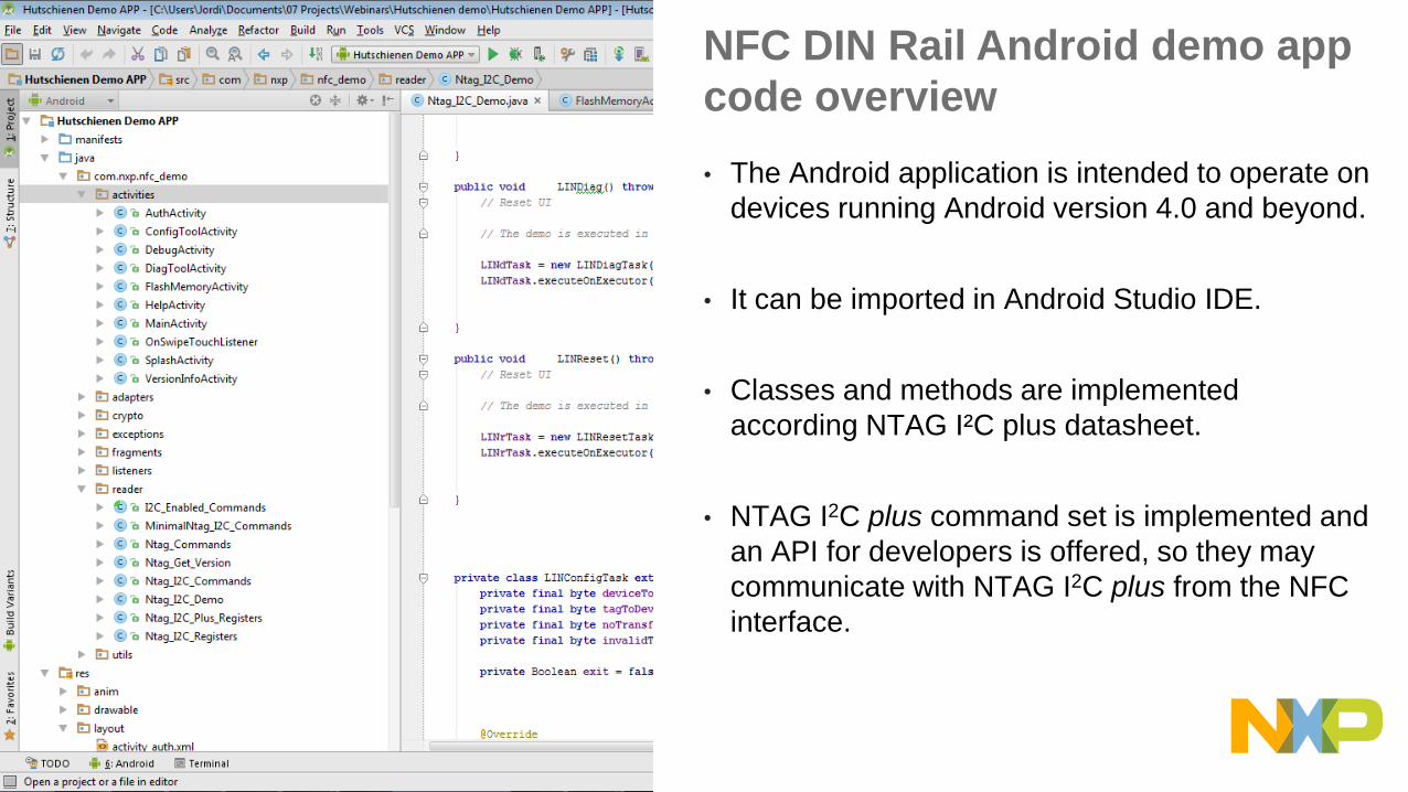
NFC DIN Rail Android demo app
code overview
• The Android application is intended to operate on
devices running Android version 4.0 and beyond.
• It can be imported in Android Studio IDE.
• Classes and methods are implemented
according NTAG I²C plus datasheet.
• NTAG I2C plus command set is implemented and
an API for developers is offered, so they may
communicate with NTAG I2C plus from the NFC
interface.

39
Useful functions dealing with NTAG I2C plus from RF interface
Memory operations (RF side)
• public void write(byte[] data, byte blockNr)
• public byte[] read(byte blockNr)
• public byte[] fast_read(byte startAddr, byte endAddr)
• public void fast_write(byte[] data, byte startAddr, byte endAddr)
• public void SectorSelect(byte sector)
• public byte[] pwdAuth(byte[] pwd)
Register operations
• public abstract byte getSessionRegisters()
• public abstract byte getConfigRegisters()
• public abstract void writeConfigRegisters(byte NC_R, byte LD_R, byte SM_R,byteWD_LS_R, byte WD_MS_R, byte I2C_CLOCK_STR)
Additional functions to deal with SRAM ( previous ones can be used as well)
• public abstract byte[] readSRAMBlock()
• public byte[] readSRAM(int blocks, R_W_Methods method)
• public void writeSRAM(byte[] data, R_W_Methods method, WriteSRAMListener listener)
• public abstract void writeSRAMBlock(byte[] data, WriteSRAMListener listener)
… and more

40
NFC DIN Rail Android demo application flow
Splash
activity
Main
activity
Zero power
configuration
activity
Diagnostics
activity
Flashing
activity
With a tap
Select binary
file to be
flashed
Select
configuration
Write EEPROM
memory
Read / Write
EEPROM
memory
Divide binary
file in chunks
of 64 bytes
Write SRAM
blocks until entire
file is transferred
With a tap
With a tap

41
EVERYTHING YOU NEED TO BUILD YOUR
PARAMETRIZATION VIA NFC SOLUTION IS HERE!

42
Summary of available resources
• Android reference source code
− http://www.nxp.com/documents/software/SW3648.zip
• MCU reference source code
− http://www.nxp.com/documents/software/SW3647.zip
• NTAG I2C plus Explorer kit
− http://www.nxp.com/products/wireless-connectivity/nfc-and-reader-ics/connected-tag-solutions/ntag-ic-plus-explorer-kit-with-nfc-reader-development-kit:OM5569-NT322ER
• NTAG I2C plus Flex kit with additional antennas
− http://www.nxp.com/products/wireless-connectivity/nfc-and-reader-ics/connected-tag-solutions/ntag-ic-plus-flex-kit-containing-additional-flex-antennas:OM5569-NT322F
• HW design files
− http://www.nxp.com/documents/software/SW3641.zip
− http://www.nxp.com/documents/software/SW3639.zip
− http://www.nxp.com/documents/software/SW3638.zip
• DIN rail module source code
− https://community.nxp.com/docs/DOC-333834

44
MIFARE® product-based applications
End-to-end systems, readers and card-related designs
EMVco applications
Readers, cards, design for test compliancy (including PCI)
Secure Element management
GlobalPlatform compliant backend solutions
Secure services provisioning OTA, TSM services
Software development in Android and iOS
Embedded software for MCUs
JCOP, Java Card operating Systems
Hardware design and development
Digital, analog, sensor acquisition, power management
Wireless communications WiFi, ZigBee, Bluetooth, BLE
Contactless antenna RF design, evaluation and testing
We help companies leverage the mobile
and contactless revolution
MobileKnowledge
Roc Boronat 117, P3M3
08018 Barcelona
(Spain)
Get in touch with us
www.themobileknowledge.com

45
Thank you for your kind attention!
Please remember to fill out our evaluation survey (pop-up)
Check your email for material download and on-demand video
addresses
Please check NXP and MobileKnowledge websites for upcoming
webinars and training sessions
http://www.nxp.com/support/classroom-training-events:CLASSROOM-TRAINING-EVENTS
www.themobileknowledge.com/content/knowledge-catalog-0
Parametrization via NFCJordi Jofre (Speaker)
Angela Gemio (Host)