Parallel Nanoshaping of Brittle Semiconductor Nanowires ... · Parallel Nanoshaping of Brittle...
9
Parallel Nanoshaping of Brittle Semiconductor Nanowires for Strained Electronics Yaowu Hu, †,‡ Ji Li, †,‡ Jifa Tian, ⊥ Yi Xuan, ‡ Biwei Deng, †,‡ Kelly L. McNear, ∥ Daw Gen Lim, # Yong Chen, ⊥ Chen Yang, ∥,⊥ and Gary J. Cheng* ,†,‡,§ † School of Industrial Engineering, Purdue University, West Lafayette, Indiana 47907, United States ‡ Birck Nanotechnology Center, Purdue University, West Lafayette, Indiana 47907, United States § School of Mechanical Engineering, Purdue University, West Lafayette, Indiana 47907, United States ∥ Department of Chemistry, Purdue University, West Lafayette, Indiana 47907, United States ⊥ Department of Physics, Purdue University, West Lafayette, Indiana 47907, United States # School of Materials Engineering, Purdue University, West Lafayette, Indiana 47907, United States * S Supporting Information ABSTRACT: Semiconductor nanowires (SCNWs) provide a unique tunability of electro-optical property than their bulk counterparts (e.g., polycrystalline thin films) due to size effects. Nanoscale straining of SCNWs is desirable to enable new ways to tune the properties of SCNWs, such as electronic transport, band structure, and quantum properties. However, there are two bottlenecks to prevent the real applications of straining engineering of SCNWs: strainability and scalability. Unlike metallic nanowires which are highly flexible and mechanically robust for parallel shaping, SCNWs are brittle in nature and could easily break at strains slightly higher than their elastic limits. In addition, the ability to generate nanoshaping in large scale is limited with the current technologies, such as the straining of nanowires with sophisticated manipulators, nanocombing NWs with U-shaped trenches, or buckling NWs with prestretched elastic substrates, which are incompatible with semiconductor technology. Here we present a top-down fabrication methodology to achieve large scale nanoshaping of SCNWs in parallel with tunable elastic strains. This method utilizes nanosecond pulsed laser to generate shock pressure and conformably deform the SCNWs onto 3D-nanostructured silicon substrates in a scalable and ultrafast manner. A polymer dielectric nanolayer is integrated in the process for cushioning the high strain-rate deformation, suppressing the generation of dislocations or cracks, and providing self-preserving mechanism for elastic strain storage in SCNWs. The elastic strain limits have been studied as functions of laser intensity, dimensions of nanowires, and the geometry of nanomolds. As a result of 3D straining, the inhomogeneous elastic strains in GeNWs result in notable Raman peak shifts and broadening, which bring more tunability of the electrical−optical property in SCNWs than traditional strain engineering. We have achieved the first 3D nanostraining enhanced germanium field-effect transistors from GeNWs. Due to laser shock induced straining effect, a more than 2-fold hole mobility enhancement and a 120% transconductance enhancement are obtained from the fabricated back-gated field effect transistors. The presented nanoshaping of SCNWs provide new ways to manipulate nanomaterials with tunable electrical−optical properties and open up many opportunities for nanoelectronics, the nanoelectrical−mechanical system, and quantum devices. KEYWORDS: Laser shock, germanium nanowires, nanoshaping, elastic strain S emiconductor nanowires (SCNWs) have unique electrical and optical properties. With the booming demand for increased packaging density and enhanced functionality of nanodevices, SCNWs are deemed as potential candidates as nanoscale building blocks for numerous applications in electronic, electromechanical, photovoltaic, optical, and opto- electronic devices. 1−8 The physical properties of SCNWs could be effectively tuned through composition modulation 9,10 or by diameter variation. 11 Elastic strain engineering, as an alternative and reversible approach, has attracted intense research interest to modulate electronic structures of SCNWs and their carrier dynamics. It has been demonstrated that SCNWs can sustain much larger strains than their bulk counterparts, due to increased mechanical strength with less defects and a larger surface/volume ratio, 12,13 promising the feasibility of strain Received: August 10, 2016 Revised: November 3, 2016 Published: November 6, 2016 Letter pubs.acs.org/NanoLett © 2016 American Chemical Society 7536 DOI: 10.1021/acs.nanolett.6b03366 Nano Lett. 2016, 16, 7536−7544
Transcript of Parallel Nanoshaping of Brittle Semiconductor Nanowires ... · Parallel Nanoshaping of Brittle...

Parallel Nanoshaping of Brittle Semiconductor Nanowires forStrained ElectronicsYaowu Hu,†,‡ Ji Li,†,‡ Jifa Tian,⊥ Yi Xuan,‡ Biwei Deng,†,‡ Kelly L. McNear,∥ Daw Gen Lim,#
Yong Chen,⊥ Chen Yang,∥,⊥ and Gary J. Cheng*,†,‡,§
†School of Industrial Engineering, Purdue University, West Lafayette, Indiana 47907, United States‡Birck Nanotechnology Center, Purdue University, West Lafayette, Indiana 47907, United States§School of Mechanical Engineering, Purdue University, West Lafayette, Indiana 47907, United States∥Department of Chemistry, Purdue University, West Lafayette, Indiana 47907, United States⊥Department of Physics, Purdue University, West Lafayette, Indiana 47907, United States#School of Materials Engineering, Purdue University, West Lafayette, Indiana 47907, United States
*S Supporting Information
ABSTRACT: Semiconductor nanowires (SCNWs) provide aunique tunability of electro-optical property than their bulkcounterparts (e.g., polycrystalline thin films) due to size effects.Nanoscale straining of SCNWs is desirable to enable new waysto tune the properties of SCNWs, such as electronic transport,band structure, and quantum properties. However, there aretwo bottlenecks to prevent the real applications of strainingengineering of SCNWs: strainability and scalability. Unlikemetallic nanowires which are highly flexible and mechanicallyrobust for parallel shaping, SCNWs are brittle in nature andcould easily break at strains slightly higher than their elasticlimits. In addition, the ability to generate nanoshaping in largescale is limited with the current technologies, such as thestraining of nanowires with sophisticated manipulators, nanocombing NWs with U-shaped trenches, or buckling NWs withprestretched elastic substrates, which are incompatible with semiconductor technology. Here we present a top-down fabricationmethodology to achieve large scale nanoshaping of SCNWs in parallel with tunable elastic strains. This method utilizesnanosecond pulsed laser to generate shock pressure and conformably deform the SCNWs onto 3D-nanostructured siliconsubstrates in a scalable and ultrafast manner. A polymer dielectric nanolayer is integrated in the process for cushioning the highstrain-rate deformation, suppressing the generation of dislocations or cracks, and providing self-preserving mechanism for elasticstrain storage in SCNWs. The elastic strain limits have been studied as functions of laser intensity, dimensions of nanowires, andthe geometry of nanomolds. As a result of 3D straining, the inhomogeneous elastic strains in GeNWs result in notable Ramanpeak shifts and broadening, which bring more tunability of the electrical−optical property in SCNWs than traditional strainengineering. We have achieved the first 3D nanostraining enhanced germanium field-effect transistors from GeNWs. Due to lasershock induced straining effect, a more than 2-fold hole mobility enhancement and a 120% transconductance enhancement areobtained from the fabricated back-gated field effect transistors. The presented nanoshaping of SCNWs provide new ways tomanipulate nanomaterials with tunable electrical−optical properties and open up many opportunities for nanoelectronics, thenanoelectrical−mechanical system, and quantum devices.
KEYWORDS: Laser shock, germanium nanowires, nanoshaping, elastic strain
Semiconductor nanowires (SCNWs) have unique electricaland optical properties. With the booming demand for
increased packaging density and enhanced functionality ofnanodevices, SCNWs are deemed as potential candidates asnanoscale building blocks for numerous applications inelectronic, electromechanical, photovoltaic, optical, and opto-electronic devices.1−8 The physical properties of SCNWs couldbe effectively tuned through composition modulation9,10 or bydiameter variation.11 Elastic strain engineering, as an alternativeand reversible approach, has attracted intense research interest
to modulate electronic structures of SCNWs and their carrierdynamics. It has been demonstrated that SCNWs can sustainmuch larger strains than their bulk counterparts, due toincreased mechanical strength with less defects and a largersurface/volume ratio,12,13 promising the feasibility of strain
Received: August 10, 2016Revised: November 3, 2016Published: November 6, 2016
Letter
pubs.acs.org/NanoLett
© 2016 American Chemical Society 7536 DOI: 10.1021/acs.nanolett.6b03366Nano Lett. 2016, 16, 7536−7544

engineering. For example, strained silicon technology has beenadopted to boost transistor performance through mobilityenhancement.14 Germanium, an indirect band gap material, canbe band gap engineered to a direct band gap of 0.34 eV at 4.2%longitudinal tensile strain,15 which greatly impacts on theluminescence behavior16 and lasing action.17 Enhancedelectronic mobility via strain engineering would pave the wayfor germanium nanowires (GeNWs) to be employed as apromising material for the channels in complementary metal−oxide−semiconductor (CMOS) devices and flexible electronics.The straining technique has been limited for a long time to
lattice mismatch which has several challenges including highdensity of defects, strain relaxation, and differences of dopingdiffusion properties.14 Alternative methods developed in recentyears, such as bending with an AFM tip or a manipulator,13,18,19
stretching in sophisticated micromechanical straining module20
or etched nanobridges,19 and buckling through a prestrainedelastic substrates such as PDMS,21,22 are beneficial forunderstanding the strain-induced physical and electricalproperty changes. However, these methods are difficult to be
implemented for practical applications in semiconductortechnology, given the fact that they are either inefficient tomanufacture on a large scale due to the one-by-onedeformation nature, or incapable of integrating reliableelectrodes and gating for the fabrication of transistors. Arecently developed nanocombing method23−25 enables aparallel deterministic assembly of kinked nanowires but islimited to water gating. It is, therefore, imperative to develop aCMOS-compatible approach to controllably deform chemicallysynthesized SCNWs in a scalable manner, thereby opening thepotential to practically implement strain engineered physicalproperties.To realize elastic straining of SCNWs, it is desirable that (a)
the strain level should be tunable and dislocations or cracksshould be avoided; (b) the elastic strain needs to be self-preserved after processing; and (c) the strained SCNWs needto be compatible with silicon technology and sit on substrateswith reliable gate modulations. In this Letter, we report on theexploitation of a laser ablation based approach with apredefined nanomold for guided elastic straining, which
Figure 1. (a) Schematic diagram showing the process flow for laser shock elastic straining of brittle semiconductor nanowires: SiO2/Si trenchesdefined by electron-beam lithography, polymer (PVP) cushion coating, transfer of SCNWs to nanomolds by (1) contact printing, (2) transferprinting, and (3) direct writing, and finally nanoshaping of SCNWs by laser shock. (b) Images of (1) SiNWs fabricated on SOI wafer, (2) stripedSCNWs on sacrificial polymer, (3) aligned SCNWs, and (4) transferred of SiNWs on nanomolds after removing polymer. (c) Image afternanshaping GeNWs by LSES and AFM image of a nanoshaped GeNW.
Nano Letters Letter
DOI: 10.1021/acs.nanolett.6b03366Nano Lett. 2016, 16, 7536−7544
7537

meets these key requirements. In previous studies, laser shockhas been demonstrated to achieve shaping of metal thin filmand nanomaterials,26−32 with the introduction of high-densitydislocations, plastic flow, and defects. However, unlike metalliccomponents which are highly flexible and mechanically robust,SCNWs are brittle in nature and could easily break at strainsslightly higher than their limits. The application of laser shockas an ultrafast approach for parallel shaping of SCNWs hasnever been exploited.Laser Shock Elastic Straining of Brittle Semiconductor
Nanowires. To solve these problems and tackle the presentlimitations, we develop a laser shock elastic straining (LSES)approach which includes four key steps (Figure 1a). First,nanoscale-channels on Si wafer are fabricated by electron-beamlithography or focused ion beam (FIB) milling. Thermalannealed SiO2 serves as back-gate dielectric for field effecttransistors (FET). Second, a thin layer of insulating polymer isdeposited on the nanostructured silicon wafer through dip/spincoating and cross-linked by thermal annealing. Polyvinylpyrro-lidone (PVP), a polymer which has been demonstrated to be ahigh-performance gate dielectric33,34 with dielectric constant35
similar to SiO2, is used in this study to serve as cushion ofnanowire shaping and elastic strain preserver. Third, SCNWs(germaniumGeNW or siliconSiNW) are grown bybottom-up vapor deposition or top-down lithography and
then transferred onto the mold surface by contact sliding36
(Figure 1a(1)), transfer printing (Figure 1a(2)), or directprinting process37 (Figure 1a(3)). As shown in Figure 1b, theSiNWs are fabricated by e-beam lithography (EBL) of silicon-on-insulator (SOI) wafer followed with dry etching Si layer andlift-off. The SiNWs were then transfer printed onto thenanomold surface. The GeNWs are grown by CVD andtransferred on to the nanomolds by contact sliding. Finally, ananosecond laser is used to generate shock wave to deform theSCNWs, defined either through bottom-up growth or top-down lithography, into the nanomolds conformally (seeMaterials and Methods in the Supporting Information).Our approach yields ultrafast elastic straining of brittle
SCNWs on silicon substrates. The GeNWs are deformedconformally onto the nanomolds by laser shock elastic straining(LSES) (see Figure 1c). No SCNWs are lost after LSES, givinga shaping yield of 100% for the GeNWs investigated (Figure S1and S2). During the LSES, an intense pressure is exerteduniformly on the nanowires, which deforms thousands ofnanowires into the mold cavities in parallel (Figure S3). Theapplication of LSES does not differentiate between bottom-upand top-down NWs or nanogeometries: once the NWs aretransferred onto the target substrate, LSES could yield effectivestraining (Figure S4). The shock pressure can be controlled bythe laser intensity, confinement, and ablative coating. The
Figure 2. (a) Schematic of GeNWs failures at geometrical sharp corners of silicon mold. (b) Schematic of LSES of GeNWs with smoothed moldcorners. Panels c and d are corresponding SEM images of a and b, respectively. (e) Molecular dynamics simulations of c, showing amorphization ofGeNW (white area) at sharp corners due to stress concentration. (f) MD simulation of deformation with self-smoothed mold corner by applyingdeformable materials as cushion (PVP). Scale bars for: (c−d) 1 μm, (e−f) 3 nm.
Nano Letters Letter
DOI: 10.1021/acs.nanolett.6b03366Nano Lett. 2016, 16, 7536−7544
7538

nanowires can be considered as free beams at suspending partsand are pinned at the bar sections by the high pressure. There isno significant sliding or turning of the nanowires on the moldsurface. Highly reliable controlled deformation in the elasticregion is critical and is realized by smooth transitions of moldgeometries and the polymer cushion. As the nanowires gain themomentum from laser shock and get deformed against thepolymer thin layer on silicon mold, viscoplastic deformation ofthe polymer consumes excessive shock energy and eliminatesstress concentration by avoiding point contacts between thebrittle SCNWs with the substrate. It should be noted that thelaser shock process takes place within tens of nanoseconds,yielding an ultrahigh strain rate not achievable in traditionalmethods. This would inhibit brittle cracking triggered byrandom imperfections on the nanowire surface in the case oflow strain rates.38 The advantage of LSES also lies in the factthat the elastically deformed SCNWs, which normally tends torelax to the unstrained state after unloading, is self-anchoredthrough van der Waals interactions between SCNWs and thepolymer thin layer, while state-of-the-art strained electricaldevices based on chemically synthesized SCNWs provide nomechanism to maintain the elastic deformation after relievingthe external loads.Interaction between the SCNWs and 3D Nano-
structured Substrates. The deformation behavior of theshocked SCNWs in LSES strongly depends on their contactswith mold surfaces. When directly shocking SCNWs on siliconor silicon dioxide surfaces, their “hard” contacts, especiallythose at the structural edges, can result in failures. Silicon moldsfabricated through wet/dry etching are typically with atomicallysharp edges, which would result in giant stress concentrationsand damages to the brittle nanowires. Although the laserpressure used is less than 1 GPa, which is lower than thestrength of the GeNWs, the stress concentration effect at thepoint or line contacts, results in much larger localized stress,
irreversible plastic deformations (amorphization) and shear-stress induced cracks, as shown schematically in Figure 2a,demonstrated experimentally in Figure 2c and numerically inFigure 2e and Figures S5 and S6. Highly localized elastic strainsin a nanowire before its failure, if any, are difficult to control.The strains are relaxed once the SCNWs are broken. In theLSES approach, we tackle this problem by employing polymercushioning and mold edge rounding. The deformationinterlayer between GeNWs and the “hard” silicon substrate;e.g., the polymer cushion creates an opportunity for softlanding of the GeNWs (Figure 2b). It provides a self-smoothingmechanism of the sharp geometries and could dynamicallyaccommodate stress distributions. We also fabricate roundededges by appropriate adjusting electron/ion beam parametersand thermal annealing. A wavy GeNW strained on a roundtrench shown in Figure 2d and f could be obtained after lasershock. By pinning the nanowire with deposited metals, wedemonstrate that the process is not due to sliding of thenanowire at mold surface, and an obvious length elongation isobserved.To further demonstrate the elastic straining of GeNWs by
LSES, high-resolution transmission electron microscopy(HRTEM) was carried out on the cross section achieved viaFIB milling of a strained GeNW petrified by PVP. Laser shockof GeNWs without PVP cushion was found to result infragmentation of brittle nanowires (Figure 3a) or large plasticdeformation due to dislocation-initiated amorphization duringultrahigh strain rate deformation (Figure 3c). When GeNWswere shocked on PVP, the deformation behavior is elastic(Figure 3b−e). We found that all of the deformation depths ofthe 3-μm-long GeNW on the three gaps, namely, D1, D2, andD3 (defined as the vertical distances between the trench centerand the gap center), are equal to 113 nm. The equivalence ofthe depths is thought-provoking. As the nanowire is not pinnedby any external forces, the boundary conditions for
Figure 3. (a) TEM images of fragmented GeNWs after shocking without PVP. (b) Tilted-view SEM image of LSES of GeNW (upper), and TEMcross-sectional view of the GeNW by FIB milling showing identical deformation depths across three trench gaps (lower). Scale bars: 1 μm and 500nm. (c) TEM image of individual GeNW by laser shock without PVP. Inset is the diffraction pattern showing amorphization of GeNW. (d−e)HRTEM images of the GeNW at the trench corners showing elastic deformation of GeNW with LSES. Inserted is the diffraction pattern. Scale bars:(a) 100 nm, (b) 1 μm and 500 nm for upper and lower images, (c) 10 nm, (d) 50 nm, and (e) 2 nm.
Nano Letters Letter
DOI: 10.1021/acs.nanolett.6b03366Nano Lett. 2016, 16, 7536−7544
7539

deformations in the three gaps are different. However, theequivalence of depths suggests that the process is self-pinned,and no significant sliding occurs between adjacent gaps.Otherwise the less constrained deformation in D3 would belarger than the other two. The self-pinning effect is due to thedeformation of the aluminum flyer and its interactions(including frictions) with GeNWs and PVP cushion, as wellas the ultrafast processing nature which petrifies themorphology instantaneously. Based on the observed nanowiremorphology, a tensile bending strain of 4.2% and a uniaxialstrain of 2.4% could be calculated, giving a maximum totalstrain of 6.6%, which are the highest strain levels to date inGeNWs based on a top-down parallel straining approach. Attrench corners, no dislocations or amorphization could beobserved on the GeNW, as shown in Figure 3d−e, which agreeswith our molecular dynamics simulations in Figure 2f anddemonstrates the elastic straining nature of LSES. We alsocarried out an experiment to investigate the strain recovery bydissolving the polymer in alcohol to release the strain;straightening of the shaped GeNWs with metal pinned at
their two ends was observed (Figure S7).The elastic straining ofLSES is thus benefited from the smooth silicon structurecorners and also the cushion performance of PVP, which avoidsstress concentrations during nanoshaping of GeNWs.
Elastic Strain Limit of GeNWs during LSES. The LSESstraining strategy generates both uniaxial tensile strain, which iscontrolled by mold geometries, and bending strain which varieswith nanowire diameters. As shown in Figure 4a, when thenanowires break at the center of trench gaps due to combinedbending and uniaxial tension stress, the maximum strains areachieved. The bending strain is estimated by39
ε = +r r R/( )1 (1)
where r and R are the nanowire radius and the radius ofbending curvature, respectively. The axial strain is determinedby
ε = L Lln( / )2 0 (2)
where L0 and L are the original and deformed segment lengthof GeNWs along the cavity in trench mold. The total strain
Figure 4. (a) Schematic of uniaxial and bending strain components introduced by laser shock. (b−c) Trends showing the dependence ofdeformation depth and total average strain as well as its components with (b) estimated laser pressure (trench width: 300 nm and GeNWs diameter:60 nm), (c) trench width (laser pressure: 940 MPa; GeNWs diameter: 60 nm), and (d) GeNW diameter (laser pressure: 940 MPa and trench width:300 nm).
Nano Letters Letter
DOI: 10.1021/acs.nanolett.6b03366Nano Lett. 2016, 16, 7536−7544
7540

could be calculated by adding the two components of strain. Asthe laser beam size is in millimeters and the beam position canbe controlled by a beam scanner, the laser shock nanoshapingprocess is a scalable technique. Depending on the mold areaand the coverage density of the GeNWs, hundreds andthousands of nanowires can be nanoshaped simultaneously witha laser pulse.We further carried out various parametric studies to validate
and establish LSES of GeNWs in particular and for SCNWs ingeneral. Experimental parameters such as (a) laser pressure, (b)trench width, and (c) GeNW diameter are varied to investigatetheir influences on deformation depths and straining levels, asshown in Figure 4b−d. The laser shock pressure values areestimated by Fabbro’s model40,41 and can be controlled byadjusting the laser intensity. It should be noted that the shockpressure, which involves dynamic responses of nanosystems, isdifferent from a hydrostatic pressure, and its actual valueapplied on the nanowires is slightly smaller than the reportedlaser shock pressure due to the attenuation in the aluminumfoil. Experiments were carried out until the fracture point ofGeNWs. It is observed that deformation depth and averagestrain increase almost linearly, with the increase in laser shockpressure as shown in Figure 4b before the nanowires attain afracture. Contributions of both bending strain (strain 1) andaxial strain (strain 2) to the total strain are also shown in Figure4b. The bending curvature has been observed to decrease withincreasing pressure. The smallest curvature attained beforefracture commences for a 60 nm nanowire is approximately 450
nm. Figure 4c and d represents the effect of trench width andGeNWs diameter on strains under constant pressure. As can beobserved from Figure 4c, the increase in the trench widthinduces higher bending and axial strains in the system. Figure4d shows the dependence of deformation depth and strain onthe nanowire diameter under constant shock pressure.Interestingly, the increase in bending strain is balanced by thedecrease in the axial strain. The bending strain increases withthe diameter, while the uniaxial one decreases, resulting in aconstant total strain over the diameter from 30 to 80 nm.
Inhomogeneous Elastic Strains in GeNWs after 3DNanoshaping. To further confirm that the elastic nature ofLSES and shed light on the strain distributions, spatiallyresolved Raman spectroscopy is employed with circularlypolarized 532 nm excitation, a 100× objective lens withnumerical aperture NA = 0.85, and a fiber coupled gratingspectrometer (2400 lines/mm). The laser intensity was keptsufficiently low to avoid heating effect. Arrays of far-isolatedridges are designed for better strain visualization. The surfacemorphology of the nanowire investigated is shown in Figure5a,b. The obtained Raman spectra around the shaped nanowire,including the Ge peak intensities and peak positions, are shownin Figure 5c,d. The silicon peaks are located at 520.1 cm−1 forall obtained spectra (Figure S8), while the Ge peaks arecontinuously blue-shifted from the ridge top to the trenchcenter (see Figure 5d), indicating a spatially varied tensilestrains. The Ge peak on the ridge is significantly broadened andhas a decreased intensity (Figure 5e), compared to the
Figure 5. Raman spectroscopy characterization of strain distribution in shaped GeNWs. (a) SEM image of the GeNW investigated. (b) AFM height(upper) and line profile (lower) measurements of the nanowire. (c) Measured Raman intensity (upper) and peak position (lower) mapping. (d)Raman spectra from 270 to 320 cm−1. The positions are indicated in panel a. (e) Measured Ge peak fwhm and intensities. (f) Simulated strain fieldsof the GeNW by FEM. (g) Plot of Raman peak shifts and calculated strains. (h) Strain variations along depth directions. Scale bars: (a) 4 μm, (b) 3μm, and (c) 1 μm.
Nano Letters Letter
DOI: 10.1021/acs.nanolett.6b03366Nano Lett. 2016, 16, 7536−7544
7541
nonshaped nanowires. The observed peak shifts are comparedwith strain fields obtained through finite element modeling(FEM), as shown in Figure 5f. The maximum peak shift of 7.1cm−1 in this nanowire corresponds to an average tensile strainof 2.4% along [111] crystallographic directions within thecircularly polarized laser spot.42−44 The peak is also significantlybroadened due to strain variations within the probed area, inboth lateral and depth directions, as shown in Figure 5g−h.Based on the AFM profiling and FEM modeling, we calculatethe elastic strain at the ridge to be 2.8%, which agrees well withthe experimental data. Similar results are obtained on otherstrained GeNWs (Figure S9), demonstrating the elasticstraining nature of the described LSES approach.Laser Shock Induced Straining Effect on FET Device
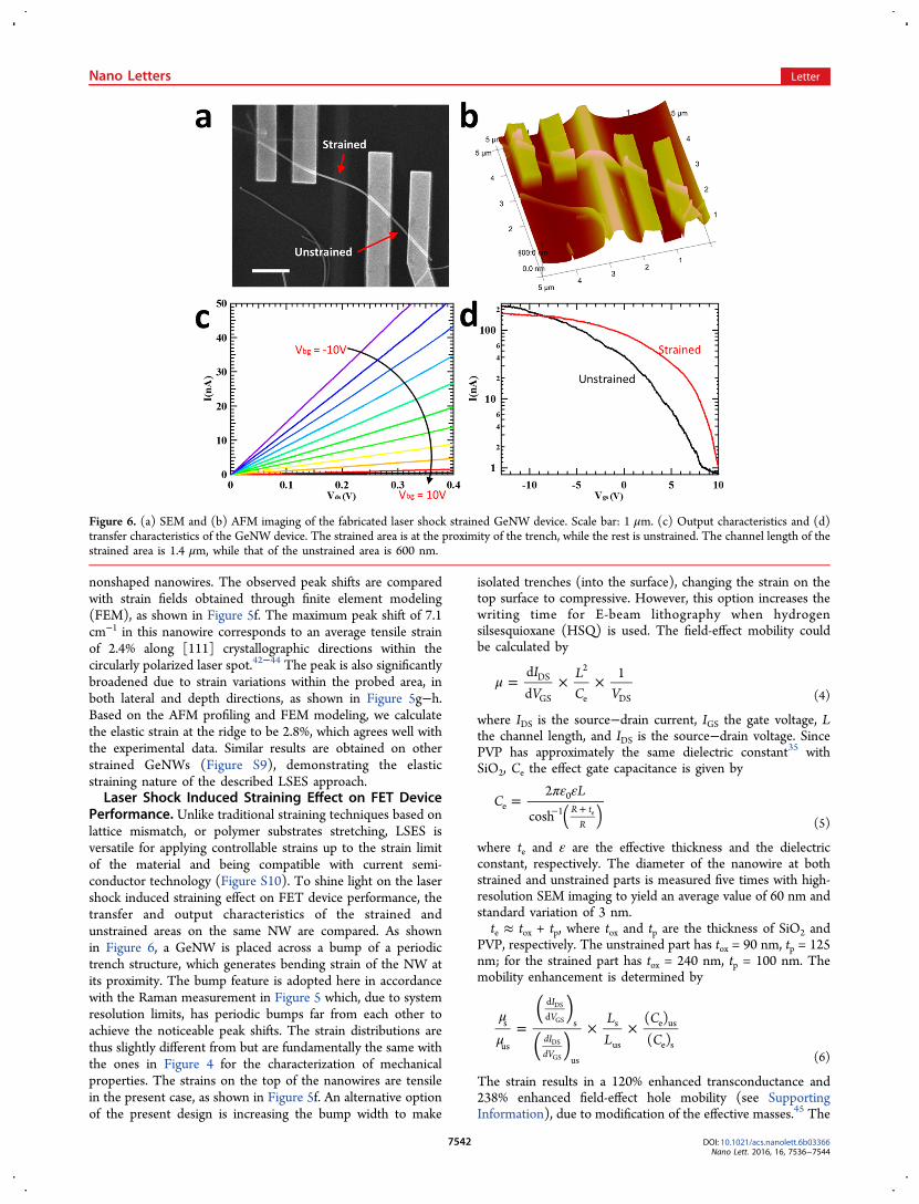
Performance. Unlike traditional straining techniques based onlattice mismatch, or polymer substrates stretching, LSES isversatile for applying controllable strains up to the strain limitof the material and being compatible with current semi-conductor technology (Figure S10). To shine light on the lasershock induced straining effect on FET device performance, thetransfer and output characteristics of the strained andunstrained areas on the same NW are compared. As shownin Figure 6, a GeNW is placed across a bump of a periodictrench structure, which generates bending strain of the NW atits proximity. The bump feature is adopted here in accordancewith the Raman measurement in Figure 5 which, due to systemresolution limits, has periodic bumps far from each other toachieve the noticeable peak shifts. The strain distributions arethus slightly different from but are fundamentally the same withthe ones in Figure 4 for the characterization of mechanicalproperties. The strains on the top of the nanowires are tensilein the present case, as shown in Figure 5f. An alternative optionof the present design is increasing the bump width to make
isolated trenches (into the surface), changing the strain on thetop surface to compressive. However, this option increases thewriting time for E-beam lithography when hydrogensilsesquioxane (HSQ) is used. The field-effect mobility couldbe calculated by
μ = × ×IV
LC V
dd
1DS
GS
2
e DS (4)
where IDS is the source−drain current, IGS the gate voltage, Lthe channel length, and IDS is the source−drain voltage. SincePVP has approximately the same dielectric constant35 withSiO2, Ce the effect gate capacitance is given by
πε ε=
− +( )C
L2
cosh R tR
e0
1 e
(5)
where te and ε are the effective thickness and the dielectricconstant, respectively. The diameter of the nanowire at bothstrained and unstrained parts is measured five times with high-resolution SEM imaging to yield an average value of 60 nm andstandard variation of 3 nm.te ≈ tox + tp, where tox and tp are the thickness of SiO2 and
PVP, respectively. The unstrained part has tox = 90 nm, tp = 125nm; for the strained part has tox = 240 nm, tp = 100 nm. Themobility enhancement is determined by
μμ
= × ×( )( )
LL
CC
( )( )
IV
dIdV
s
us
dd s
us
s
us
e us
e s
DS
GS
DS
GS (6)
The strain results in a 120% enhanced transconductance and238% enhanced field-effect hole mobility (see SupportingInformation), due to modification of the effective masses.45 The
Figure 6. (a) SEM and (b) AFM imaging of the fabricated laser shock strained GeNW device. Scale bar: 1 μm. (c) Output characteristics and (d)transfer characteristics of the GeNW device. The strained area is at the proximity of the trench, while the rest is unstrained. The channel length of thestrained area is 1.4 μm, while that of the unstrained area is 600 nm.
Nano Letters Letter
DOI: 10.1021/acs.nanolett.6b03366Nano Lett. 2016, 16, 7536−7544
7542

device on/off ratio is also found to be decreased from 2.77 ×10² to 1.76 × 10², agreeing with the band gap shrinkage underthe presence of both tensile and compressive strains. A similarphenomenon was found in several other nanowires from thesame batch and same nanomold after laser straining, with amobility increase by 230−260%, and a transconductanceincrease by 120−150%. The on/off ratio was decreased byabout 30−40%. It should be noted that these values could varywhen different mold structural dimensions and laser parametersare applied, as they effectively tune the three-dimensionalstrains and strain gradients. As the thicknesses of gatedielectrics for the strained and unstrained devices are different,the device performance could be further boosted by adoptingconformal top gating. In principle, the strain fields of theSCNWs could be designed by adjusting laser parameters andmold geometries, yielding tunable band structure engineering,the details of which are beyond the scope of the current workand leave large room for future device performanceoptimization.In conclusion, we have demonstrated for the first time that
brittle SCNWs can be nanoshaped at ultrahigh strain rate in anultrafast and controllable manner. This method utilizes laser-induced shock loading to deform SCNWs onto 3D-nano-structured silicon substrates with a cushioning polymerdielectric nanolayer, resulting in the storage of elastic strainsin SCNWs without dislocations or cracks. The elastic strainingachieved by LSES is self-preserved and CMOS-compatible. Wehave studied the effects of processing parameters, such as moldgeometries (e.g., corner sharpness and trench width), laserpressure, and nanowire diameters, on the deformation behaviorand elastic strain limits. The elastic strains of GeNWs areexperimentally investigated by spatially resolved Ramanspectroscopy and TEM and confirmed by numericalsimulations at both atomic and continuum-mechanics scales.The tunable strains resulted in SCNWs can be controlled bythe laser intensity, dimensions of nanowires, and geometry ofnanomolds. As a result of 3D straining, the inhomogeneouselastic strains in GeNWs results in notable Raman peak shiftsand broadening, which bring more tunability of electrical-optical property in SCNWs than traditional strain engineering.Nanowire FETs are fabricated with LSES treated GeNWs, andit is found to yield significantly enhanced hole mobilities andmodulated on/off ratios. This laser-based nanoshapingtechnique is versatile and suitable for variety of semiconductornanowires and other 1D nanostructures. The findings in thisstudy would potentially bring many breakthroughs in future, asit provides a clean technology for band engineering of SCNWsfor large-scale applications.
■ ASSOCIATED CONTENT
*S Supporting InformationThe Supporting Information is available free of charge on theACS Publications website at DOI: 10.1021/acs.nano-lett.6b03366.
Materials and methods, AFM images of the sameGeNWs before and after laser shock, MD simulation ofshear stress concentration at sharp mold corners, cycledshaping with laser shock and polymer dissolving, Ramanspectra of GeNWs at germanium peaks and silicon peaks,fabricated strained GeNW FET with a large on/off ratio,and methods for mobility calculations (PDF)
■ AUTHOR INFORMATION
Corresponding Author*Phone: 765 49-45436, e-mail: [email protected].
ORCID
Jifa Tian: 0000-0003-2921-470XGary J. Cheng: 0000-0002-1184-2946NotesThe authors declare no competing financial interest.
■ ACKNOWLEDGMENTS
We sincerely thank the US National Science Foundationthrough CMMI (grant number 1538360) for financial supportand the Purdue Office of Vice President for Research throughan incentive research grant.
■ REFERENCES(1) Ionescu, A. M. Electronic Devices: Nanowire Transistors MadeEasy. Nat. Nanotechnol. 2010, 5, 178−179.(2) Xu, S.; Qin, Y.; Xu, C.; Wei, Y.; Yang, R.; Wang, Z. L. Self-Powered Nanowire Devices. Nat. Nanotechnol. 2010, 5, 366−373.(3) Ju, S.; Facchetti, A.; Xuan, Y.; Liu, J.; Ishikawa, F.; Ye, P.; Zhou,C.; Marks, T. J.; Janes, D. B. Fabrication of Fully TransparentNanowire Transistors for Transparent and Flexible Electronics. Nat.Nanotechnol. 2007, 2, 378−384.(4) Husain, A.; Hone, J.; Postma, H. W. C.; Huang, X. M. H.; Drake,T.; Barbic, M.; Scherer, A.; Roukes, M. L. Nanowire-Based Very-High-Frequency Electromechanical Resonator. Appl. Phys. Lett. 2003, 83,1240−1242.(5) Adachi, M. M.; Anantram, M. P.; Karim, K. S. Core-Shell SiliconNanowire Solar Cells. Sci. Rep. 2013, 3, 2−7.(6) Cao, L.; White, J. S.; Park, J.-S.; Schuller, J. A.; Clemens, B. M.;Brongersma, M. L. Engineering Light Absorption in SemiconductorNanowire Devices. Nat. Mater. 2009, 8, 643−647.(7) Babinec, T. M.; Hausmann, B. J. M.; Khan, M.; Zhang, Y.; Maze,J. R.; Hemmer, P. R.; Loncar, M. A Diamond Nanowire Single-PhotonSource. Nat. Nanotechnol. 2010, 5, 195−199.(8) Li, Y.; Qian, F.; Xiang, J.; Lieber, C. M. Nanowire Electronic andOptoelectronic Devices. Mater. Today 2006, 9, 18−27.(9) Gu, F.; Yang, Z.; Yu, H.; Xu, J.; Wang, P.; Tong, L.; Pan, A.Spatial Bandgap Engineering along Single Alloy Nanowires. J. Am.Chem. Soc. 2011, 133, 2037−2039.(10) Shin, J. C.; Kim, K. H.; Yu, K. J.; Hu, H.; Yin, L.; Ning, C.;Rogers, J. A.; Zuo, J.; Li, X. In X Ga 1- X As Nanowires on Silicon:One-Dimensional Heterogeneous Epitaxy, Bandgap Engineering, andPhotovoltaics. Nano Lett. 2011, 11, 4831−4838.(11) Myalitsin, A.; Strelow, C.; Wang, Z.; Li, Z.; Kipp, T.; Mews, A.ACS Nano 2011, 5, 7920−7927.(12) Smith, D. A.; Holmberg, V. C.; Lee, D. C.; Korgel, B. A. Young’sModulus and Size-Dependent Mechanical Quality Factor of Nano-electromechanical Germanium Nanowire Resonators. J. Phys. Chem. C2008, 112, 10725−10729.(13) Hoffmann, S.; Utke, I.; Moser, B.; Michler, J.; Christiansen, S.H.; Schmidt, V.; Senz, S.; Werner, P.; Gosele, U.; Ballif, C.Measurement of the Bending Strength of Vapor-Liquid-Solid GrownSilicon Nanowires. Nano Lett. 2006, 6, 622−625.(14) Ieong, M. Silicon Device Scaling to the Sub-10-Nm Regime.Science (Washington, DC, U. S.) 2004, 306, 2057−2060.(15) Zhang, F.; Crespi, V. H.; Zhang, P. Prediction That UniaxialTension along 111 Produces a Direct Band Gap in Germanium. Phys.Rev. Lett. 2009, 102, 1−4.(16) Audoit, G.; Mhuircheartaigh, E. N.; Lipson, S. M.; Morris, M.A.; Blau, W. J.; Holmes, J. D. Strain Induced Photoluminescence fromSilicon and Germanium Nanowire Arrays. J. Mater. Chem. 2005, 15,4809.
Nano Letters Letter
DOI: 10.1021/acs.nanolett.6b03366Nano Lett. 2016, 16, 7536−7544
7543

(17) Liu, J.; Sun, X.; Camacho-Aguilera, R.; Kimerling, L. C.; Michel,J. Ge-on-Si Laser Operating at Room Temperature. Opt. Lett. 2010,35, 679−681.(18) Smith, D. A.; Holmberg, V. C.; Korgel, B. A. FlexibleGermanium Nanowires: Ideal Strength, Room Temperature Plasticity,and Bendable Semiconductor Fabric. ACS Nano 2010, 4, 2356−2362.(19) Suess, M. J.; Geiger, R.; Minamisawa, R. A.; Schiefler, G.;Frigerio, J.; Chrastina, D.; Isella, G.; Spolenak, R.; Faist, J.; Sigg, H.Analysis of Enhanced Light Emission from Highly StrainedGermanium Microbridges. Nat. Photonics 2013, 7, 466−472.(20) Greil, J.; Lugstein, A.; Zeiner, C.; Strasser, G.; Bertagnolli, E.Tuning the Electro-Optical Properties of Germanium Nanowires byTensile Strain. Nano Lett. 2012, 12, 6230−6234.(21) Ryu, S. Y.; Xiao, J.; Park, W. Il; Son, K. S.; Huang, Y. Y.; Paik,U.; Rogers, J. A. Lateral Buckling Mechanics in Silicon Nanowires onElastomeric Substrates. Nano Lett. 2009, 9, 3214−3219.(22) Xu, F.; Lu, W.; Zhu, Y. Controlled 3D Buckling of SiliconNanowires for Stretchable Electronics. ACS Nano 2011, 5, 672−678.(23) Yao, J.; Yan, H.; Lieber, C. M. A Nanoscale Combing Techniquefor the Large-Scale Assembly of Highly Aligned Nanowires. Nat.Nanotechnol. 2013, 8, 329−335.(24) Yao, J.; Yan, H.; Das, S.; Klemic, J. F.; Ellenbogen, J. C.; Lieber,C. M. Nanowire Nanocomputer as a Finite-State Machine. Proc. Natl.Acad. Sci. U. S. A. 2014, 111, 2431−2435.(25) Zhao, Y.; Yao, J.; Xu, L.; Mankin, M. N.; Zhu, Y.; Wu, H.; Mai,L.; Zhang, Q.; Lieber, C. M. Shape-Controlled Deterministic Assemblyof Nanowires. Nano Lett. 2016, 16, 2644.(26) Hu, Y.; Kumar, P.; Xu, R.; Zhao, K.; Cheng, G. J. UltrafastDirect Fabrication of Flexible Substrate-Supported Designer Plas-monic Nanoarrays. Nanoscale 2016, 8, 172−182.(27) Gao, H.; Hu, Y.; Xuan, Y.; Li, J.; Yang, Y.; Martinez, R. V.; Li,C.; Luo, J.; Qi, M.; Cheng, G. J. Large-Scale Nanoshaping ofUltrasmooth 3D Crystalline Metallic Structures. Science (Washington,DC, U. S.) 2014, 346, 1352−1356.(28) Kumar, P.; Li, J.; Nian, Q.; Hu, Y.; Cheng, G. J. PlasmonicTuning of Silver Nanowires by Laser Shock Induced LateralCompression. Nanoscale 2013, 5, 6311.(29) Hu, Y.; Lee, S.; Kumar, P.; Nian, Q.; Wang, W.; Irudayaraj, J. J.;Cheng, G. J. Water Flattens Graphene Wrinkles: Laser ShockWrapping of Graphene onto Substrate-Supported CrystallinePlasmonic Nanoparticle Arrays. Nanoscale 2015, 7, 19885.(30) Li, J.; Liao, Y.; Suslov, S.; Cheng, G. J. Laser Shock-BasedPlatform for Controllable Forming of Nanowires. Nano Lett. 2012, 12,3224−3230.(31) Hu, Y.; Kumar, P.; Xuan, Y.; Deng, B.; Qi, M.; Cheng, G. J.Controlled and Stabilized Light-Matter Interaction in Graphene:Plasmonic Film with Large-Scale 10-Nm Lithography. Adv. Opt. Mater.2016, DOI: 10.1002/adom.201600201.(32) Hu, Y.; Xuan, Y.; Wang, X.; Deng, B.; Saei, M.; Jin, S.;Irudayaraj, J.; Cheng, G. J. Superplastic Forming of MetalNanostructure Arrays with Ultrafine Gaps. Adv. Mater. 2016, 28, 1−11.(33) Roberts, M. E.; Queralto, N.; Mannsfeld, S. C. B.; Reinecke, B.N.; Knoll, W.; Bao, Z. Cross-Linked Polymer Gate Dielectric Films forLow-Voltage Organic Transistors. Chem. Mater. 2009, 21, 2292−2299.(34) Klauk, H.; Halik, M.; Zschieschang, U.; Schmid, G.; Radlik, W.;Weber, W. High-Mobility Polymer Gate Dielectric Pentacene ThinFilm Transistors. J. Appl. Phys. 2002, 92, 5259.(35) Chen, F. C.; Chu, C. W.; He, J.; Yang, Y.; Lin, J. L. OrganicThin-Film Transistors with Nanocomposite Dielectric Gate Insulator.Appl. Phys. Lett. 2004, 85, 3295−3297.(36) Javey, A.; Nam, S.; Friedman, R. S.; Yan, H.; Lieber, C. M.Layer-by-Layer Assembly of Nanowires for Three-Dimensional,Multifunctional Electronics. Nano Lett. 2007, 7, 773−777.(37) Carlson, A.; Bowen, A. M.; Huang, Y.; Nuzzo, R. G.; Rogers, J. a.Transfer Printing Techniques for Materials Assembly and Micro/nanodevice Fabrication. Adv. Mater. 2012, 24, 5284−5318.(38) Ramachandramoorthy, R.; Gao, W.; Bernal, R.; Espinosa, H.High Strain Rate Tensile Testing of Silver Nanowires: Rate-Dependent Brittle-to-Ductile Transition. Nano Lett. 2016, 16, 255.
(39) Zhang, Z.; Han, X. D.; Zhang, Y. F.; Zheng, K.; Zhang, X. N.;Hao, Y. J.; Guo, X. Y.; Yuan, J.; Wang, Z. L. Low-Temperature in SituLarge Strain Plasticity of Ceramic SiC Nanowires and Its Atomic-ScaleMechanism. Nano Lett. 2007, 7, 452−457.(40) Fabbro, R.; Fournier, J.; Ballard, P.; Devaux, D.; Virmont, J.Physical Study of Laser-Produced Plasma in Confined Geometry. J.Appl. Phys. 1990, 68, 775.(41) Devaux, D.; Fabbro, R.; Tollier, L.; Bartnicki, E. Generation ofShock Waves by Laser-Induced Plasma in Confined Geometry. J. Appl.Phys. 1993, 74, 2268−2273.(42) Peng, C. Y.; Huang, C. F.; Fu, Y. C.; Yang, Y. H.; Lai, C. Y.;Chang, S. T.; Liu, C. W. Comprehensive Study of the Raman Shifts ofStrained Silicon and Germanium. J. Appl. Phys. 2009, 105, 083537.(43) Suess, M. J.; Minamisawa, R. A.; Geiger, R.; Bourdelle, K. K.;Sigg, H.; Spolenak, R. Power-Dependent Raman Analysis of HighlyStrained Si Nanobridges. Nano Lett. 2014, 14, 1249.(44) Suess, M. J.; Geiger, R.; Minamisawa, R. a.; Schiefler, G.;Frigerio, J.; Chrastina, D.; Isella, G.; Spolenak, R.; Faist, J.; Sigg, H.Analysis of Enhanced Light Emission from Highly StrainedGermanium Microbridges. Nat. Photonics 2013, 7, 466−472.(45) Riddet, C.; Watling, J. R.; Chan, K. H.; Parker, E. H. C.; Whall,T. E.; Leadley, D. R.; Asenov, A. Hole Mobility in Germanium as aFunction of Substrate and Channel Orientation, Strain, Doping, andTemperature. IEEE Trans. Electron Devices 2012, 59, 1878−1884.
Nano Letters Letter
DOI: 10.1021/acs.nanolett.6b03366Nano Lett. 2016, 16, 7536−7544
7544