PADS to Stackup Planner Interface - iCD | Home · PADS’ Layer Thickness dialog should be visible...
4
AN2013_7 PADS Layout/Stackup Planner Bidirectional Interface © 2013 In-Circuit Design Pty Ltd | Australia Page 1 The Stackup Planner/PADS Layout bidirectional interface exports PADS Electrical Layers into ICD Stackup Planner for the calculation of impedance and trace current. The stackup can then be modified in Stackup Planner—to obtain the desired impedances—and imported back into PADS Layout. Licensing: A 14-day license is included with download. Contact [email protected] for permanent license. Importing a Stackup from PADS Layout into ICD Stackup Planner: Whether you’re starting with a legacy stackup in PADS, or a default stackup that needs refinement and impedance planning—based on actual dielectric materials, thicknesses, and dielectric constants—ICD Stackup Planner is an ideal companion product for PADS users. To bring a substrate design into Stackup Planner from PADS, perform the following steps: 1. Open the PCB database in PADS Layout, and select File > Export > Save. 2. The ASCII Output dialog opens, as shown above. 3. Click the Select All button, and OK. An .ASC file is created, exporting everything in the PADS database, including both Electrical Layers and General Layers. 4. Open ICD Stackup Planner. 5. To import the Electrical Layers from the PADS ASCII file into ICD Stackup Planner, select Import > EDA Translators > PADS, and navigate to the PADS ASC file, as shown on the following page. 6. A new stackup tab will appear in Stackup Planner, using the following decision rules for dielectric layer creation: • PADS dielectric layers default to Substrate. Substrate layers in PADS will result in Core layers in Stackup Planner. • If a dielectric layer is identified as a Prepreg layer in PADS, this will be assigned as a Prepreg layer in Stackup Planner. • If a dielectric layer is identified as a Solder Mask layer in PADS, this will be assigned as a Solder Mask layer in Stackup Planner.
-
Upload
nguyenxuyen -
Category
Documents
-
view
216 -
download
0
Transcript of PADS to Stackup Planner Interface - iCD | Home · PADS’ Layer Thickness dialog should be visible...

AN2013_7 PADS Layout/Stackup Planner Bidirectional Interface
© 2013 In-Circuit Design Pty Ltd | Australia Page 1
The Stackup Planner/PADS Layout bidirectional interface exports PADS Electrical Layers into
ICD Stackup Planner for the calculation of impedance and trace current. The stackup can then be
modified in Stackup Planner—to obtain the desired impedances—and imported back into PADS
Layout.
Licensing: A 14-day license is included with download. Contact [email protected] for permanent license.
Importing a Stackup from PADS Layout into ICD Stackup Planner: Whether you’re starting with a legacy stackup in PADS, or a default stackup that needs
refinement and impedance planning—based on actual dielectric materials, thicknesses, and
dielectric constants—ICD Stackup Planner is an ideal companion product for PADS users.
To bring a substrate design into Stackup Planner from PADS, perform the following steps:
1. Open the PCB database in PADS Layout, and select File > Export > Save.
2. The ASCII Output dialog opens, as shown above.
3. Click the Select All button, and OK. An .ASC file is created, exporting everything in the
PADS database, including both Electrical Layers and General Layers.
4. Open ICD Stackup Planner.
5. To import the Electrical Layers from the PADS ASCII file into ICD Stackup Planner, select
Import > EDA Translators > PADS, and navigate to the PADS ASC file, as shown on the
following page.
6. A new stackup tab will appear in Stackup Planner, using the following decision rules for
dielectric layer creation:
• PADS dielectric layers default to Substrate. Substrate layers in PADS will result in
Core layers in Stackup Planner.
• If a dielectric layer is identified as a Prepreg layer in PADS, this will be assigned as a
Prepreg layer in Stackup Planner.
• If a dielectric layer is identified as a Solder Mask layer in PADS, this will be assigned
as a Solder Mask layer in Stackup Planner.

AN2013_7 PADS Layout/Stackup Planner Bidirectional Interface
© 2013 In-Circuit Design Pty Ltd | Australia Page 2
7. Note that PADS defaults to all dielectric layers as “Substrate,” with dielectric constants of
4.3 and dielectric thicknesses of 10 mils, as shown above.
8. The new stackup will show the following for metal-layer creation:
• If a metal layer is identified as a Routing layer in PADS, this will result in a signal
layer in Stackup Planner. Signal layers in this version of the PADS interface assign trace widths to 4 mils, with differential clearances of 8 mils in Stackup Planner.
• If a metal layer is identified as a CAM Plane in PADS, this will be a Plane layer in
Stackup Planner.
AN2013_7 PADS Layout/Stackup Planner Bidirectional Interface
© 2013 In-Circuit Design Pty Ltd | Australia Page 3
• If a metal layer is identified as a Split/Mixed layer in PADS, this will result as a Plane
layer in Stackup Planner. (More options on Split/Mixed layers will be provided in a
future release. In the meantime, right click on a layer, and select Swap Plane/Signal
to toggle back and forth for impedance calculations.)
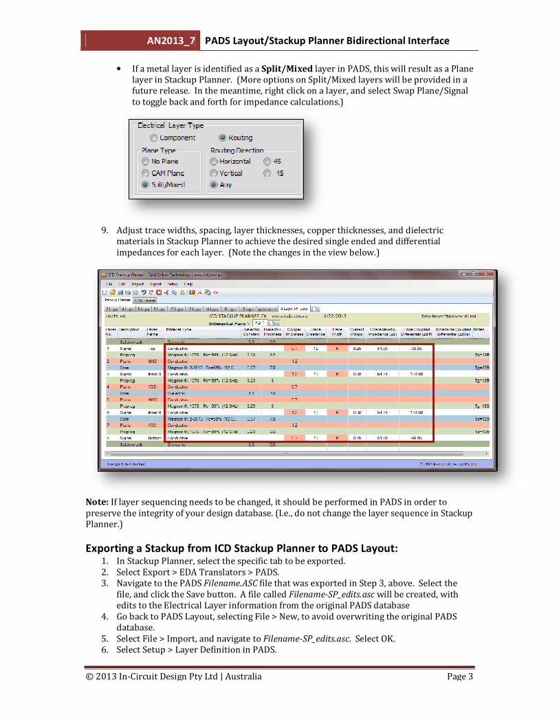
9. Adjust trace widths, spacing, layer thicknesses, copper thicknesses, and dielectric
materials in Stackup Planner to achieve the desired single ended and differential
impedances for each layer. (Note the changes in the view below.)
Note: If layer sequencing needs to be changed, it should be performed in PADS in order to
preserve the integrity of your design database. (I.e., do not change the layer sequence in Stackup
Planner.)
Exporting a Stackup from ICD Stackup Planner to PADS Layout: 1. In Stackup Planner, select the specific tab to be exported.
2. Select Export > EDA Translators > PADS.
3. Navigate to the PADS Filename.ASC file that was exported in Step 3, above. Select the
file, and click the Save button. A file called Filename-SP_edits.asc will be created, with
edits to the Electrical Layer information from the original PADS database
4. Go back to PADS Layout, selecting File > New, to avoid overwriting the original PADS
database.
5. Select File > Import, and navigate to Filename-SP_edits.asc. Select OK.
6. Select Setup > Layer Definition in PADS.

AN2013_7 PADS Layout/Stackup Planner Bidirectional Interface
© 2013 In-Circuit Design Pty Ltd | Australia Page 4
7. Select the Thickness button to open the Layer Thickness dialog.
Verifying Stackup Changes in PADS:
1. Press the Windows button on your keyboard (next to the ALT button), and the left
arrow simultaneously.
2. Press ALT and Tab to select Stackup Planner; then press the Windows button again, and
the right arrow simultaneously. PADS’ Layer Thickness dialog should be visible on the
left half of the screen, and Stackup Planner on the right half, as shown below.
3. Verify that the layer thicknesses, copper thicknesses, and dielectric constants are the
same. (Note; Stackup Planner will not change layer names in PADS.)
Note: An upcoming revision to the PADS-to-Stackup Planner import will include default trace
widths and clearances from PADS. The export to PADS will include net-class rules that can be
conditionally assigned in PADS.