
PA04 • PA04A - Power Operational Amplifers · The PA04 is a high voltage MOSFET power operational...
14
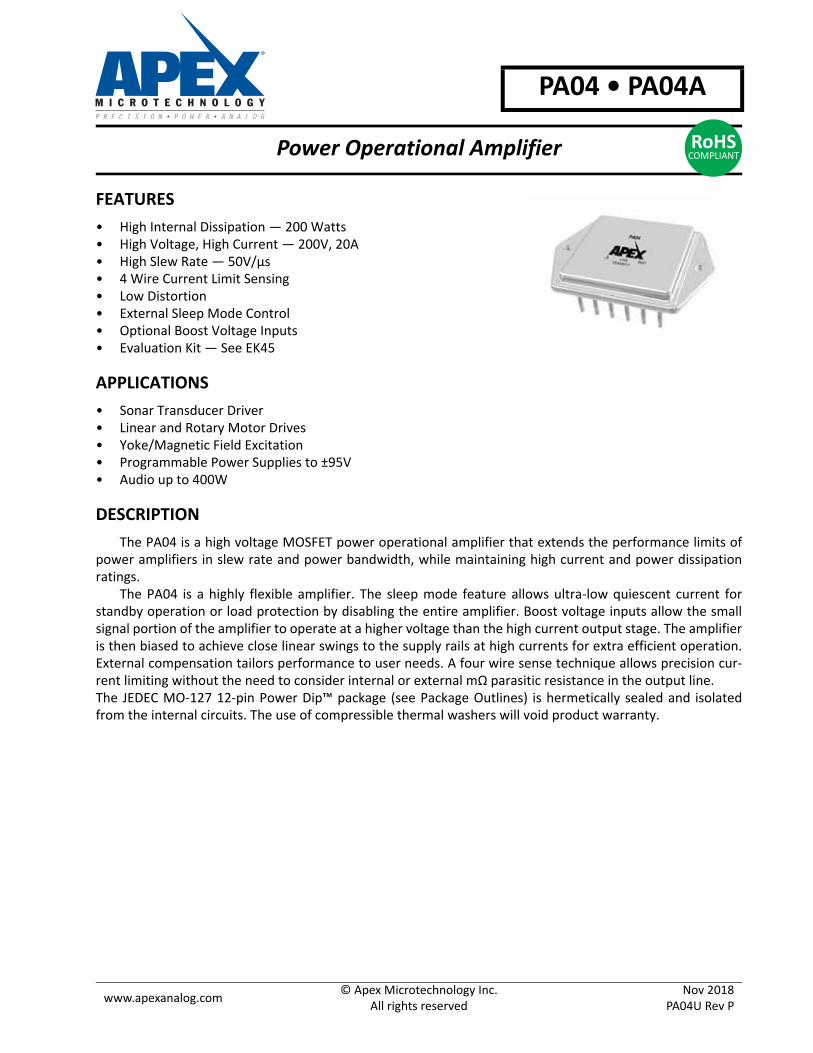
PA04 • PA04A www.apexanalog.com © Apex Microtechnology Inc. All rights reserved Nov 2018 PA04U Rev P Power Operational Amplifier RoHS COMPLIANT FEATURES • High Internal Dissipation — 200 Watts • High Voltage, High Current — 200V, 20A • High Slew Rate — 50V/µs • 4 Wire Current Limit Sensing • Low Distortion • External Sleep Mode Control • Optional Boost Voltage Inputs • Evaluation Kit — See EK45 APPLICATIONS • Sonar Transducer Driver • Linear and Rotary Motor Drives • Yoke/Magnetic Field Excitation • Programmable Power Supplies to ±95V • Audio up to 400W DESCRIPTION The PA04 is a high voltage MOSFET power operational amplifier that extends the performance limits of power amplifiers in slew rate and power bandwidth, while maintaining high current and power dissipation ratings. The PA04 is a highly flexible amplifier. The sleep mode feature allows ultra-low quiescent current for standby operation or load protection by disabling the entire amplifier. Boost voltage inputs allow the small signal portion of the amplifier to operate at a higher voltage than the high current output stage. The amplifier is then biased to achieve close linear swings to the supply rails at high currents for extra efficient operation. External compensation tailors performance to user needs. A four wire sense technique allows precision cur- rent limiting without the need to consider internal or external mΩ parasitic resistance in the output line. The JEDEC MO-127 12-pin Power Dip™ package (see Package Outlines) is hermetically sealed and isolated from the internal circuits. The use of compressible thermal washers will void product warranty.
Transcript of PA04 • PA04A - Power Operational Amplifers · The PA04 is a high voltage MOSFET power operational...
www.apexanalog.com© Apex Microtechnology Inc
All rights reserved
Power Operational Am
PA04 • PA04A
plifier RoHSCOMPLIANT
FEATURES
• High Internal Dissipation — 200 Watts• High Voltage, High Current — 200V, 20A• High Slew Rate — 50V/µs• 4 Wire Current Limit Sensing• Low Distortion• External Sleep Mode Control• Optional Boost Voltage Inputs• Evaluation Kit — See EK45
APPLICATIONS
• Sonar Transducer Driver• Linear and Rotary Motor Drives• Yoke/Magnetic Field Excitation• Programmable Power Supplies to ±95V• Audio up to 400W
DESCRIPTION
The PA04 is a high voltage MOSFET power operational amplifier that extends the performance limits of power amplifiers in slew rate and power bandwidth, while maintaining high current and power dissipation ratings.
The PA04 is a highly flexible amplifier. The sleep mode feature allows ultra-low quiescent current for standby operation or load protection by disabling the entire amplifier. Boost voltage inputs allow the small signal portion of the amplifier to operate at a higher voltage than the high current output stage. The amplifier is then biased to achieve close linear swings to the supply rails at high currents for extra efficient operation. External compensation tailors performance to user needs. A four wire sense technique allows precision cur-rent limiting without the need to consider internal or external mΩ parasitic resistance in the output line.The JEDEC MO-127 12-pin Power Dip™ package (see Package Outlines) is hermetically sealed and isolated from the internal circuits. The use of compressible thermal washers will void product warranty.
. Nov 2018PA04U Rev P

PA04 • PA04A
Figure 1: Equivalent Schematic
12
9
1
5 6
8
10
11
7
2
4
3
SLEEP
+VB
Q10
–IN
Q14 Q15
Q21
–VBCOMP
Q22
+IN
Q20
COMP
Q17
D1
Q5
Q12
Q19
Q26
Q18
Q13
+VS
Q6
OUTQ7
–VS
D5 D6
D2D3
D7D9
D8
D4ICL
ICL
TYPICAL CONNECTION
Figure 2: Typical Connection
*
*
* Use 10μF per Amp of output current
2 PA04U Rev P
PA04 • PA04A
PINOUT AND DESCRIPTION TABLE
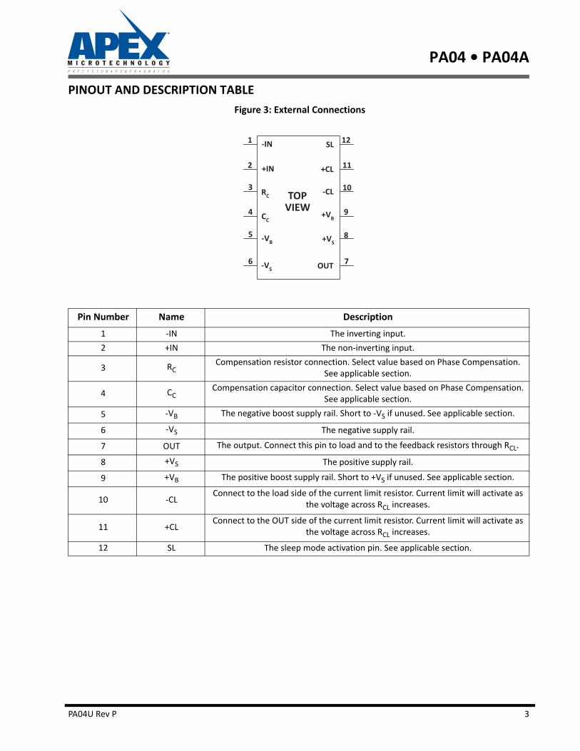
Figure 3: External Connections
Pin Number Name Description
1 -IN The inverting input.
2 +IN The non-inverting input.
3 RCCompensation resistor connection. Select value based on Phase Compensation.
See applicable section.
4 CCCompensation capacitor connection. Select value based on Phase Compensation.
See applicable section.
5 -VB The negative boost supply rail. Short to -VS if unused. See applicable section.
6 -VS The negative supply rail.
7 OUT The output. Connect this pin to load and to the feedback resistors through RCL.
8 +VS The positive supply rail.
9 +VB The positive boost supply rail. Short to +VS if unused. See applicable section.
10 -CLConnect to the load side of the current limit resistor. Current limit will activate as
the voltage across RCL increases.
11 +CLConnect to the OUT side of the current limit resistor. Current limit will activate as
the voltage across RCL increases.
12 SL The sleep mode activation pin. See applicable section.
PA04U Rev P 3

PA04 • PA04A
SPECIFICATIONS
Unless otherwise noted: TC = 25°C, CC = 470pF, RC = 120 Ω. DC input specifications are ± value given. Power
supply voltage is typical rating. ±VB = ±VS.
ABSOLUTE MAXIMUM RATINGS
Parameter Symbol Min Max Units
Supply Voltage, total +Vs to -Vs 200 V
Boost Voltage ±VB ±VS ± 20V V
Output Current, within SOA IOUT 20 A
Power Dissipation, internal PD 200 W
Input Voltage, differential VIN (Diff) -20 20 V
Input Voltage, common mode VCM -VS VS V
Temperature, pin solder, 10s 350 °C
Temperature, junction 1
1. Long term operation at the maximum junction temperature will result in reduced product life. Derate internal power dis-sipation to achieve high MTTF. For guidance, refer to the heatsink data sheet.
TJ 150 °C
Temperature, storage -65 +150 °C
Operating Temperature Range, case TC -55 +125 °C
CAUTION
The PA04 is constructed from MOSFET transistors. ESD handling procedures must be observed.The internal substrate contains beryllia (BeO). Do not break the seal. If accidentally broken, do not crush, machine, or subject to temperatures in excess of 850°C to avoid generating toxic fumes.
4 PA04U Rev P
PA04 • PA04A
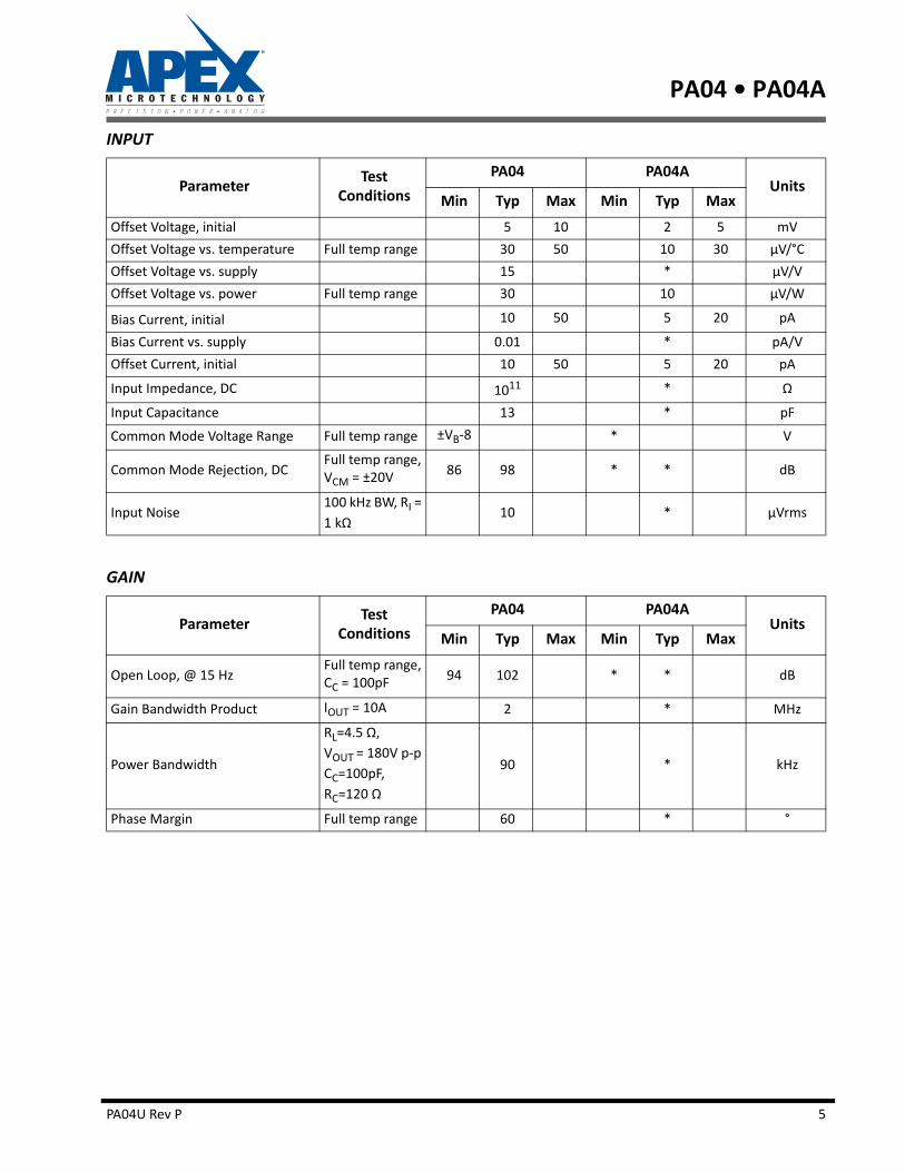
INPUT
ParameterTest
Conditions
PA04 PA04AUnits
Min Typ Max Min Typ Max
Offset Voltage, initial 5 10 2 5 mV
Offset Voltage vs. temperature Full temp range 30 50 10 30 µV/°C
Offset Voltage vs. supply 15 * µV/V
Offset Voltage vs. power Full temp range 30 10 µV/W
Bias Current, initial 10 50 5 20 pA
Bias Current vs. supply 0.01 * pA/V
Offset Current, initial 10 50 5 20 pA
Input Impedance, DC 1011 * Ω
Input Capacitance 13 * pF
Common Mode Voltage Range Full temp range ±VB-8 * V
Common Mode Rejection, DCFull temp range, VCM = ±20V
86 98 * * dB
Input Noise100 kHz BW, RI =
1 kΩ10 * µVrms
GAIN
ParameterTest
Conditions
PA04 PA04AUnits
Min Typ Max Min Typ Max
Open Loop, @ 15 HzFull temp range, CC = 100pF
94 102 * * dB
Gain Bandwidth Product IOUT = 10A 2 * MHz
Power Bandwidth
RL=4.5 Ω,VOUT = 180V p-pCC=100pF,
RC=120 Ω
90 * kHz
Phase Margin Full temp range 60 * °
PA04U Rev P 5

PA04 • PA04A
OUTPUT
ParameterTest
Conditions
PA04 PA04AUnits
Min Typ Max Min Typ Max
Voltage Swing IOUT = 15A ±VS-8.8 ±VS-7.5 * * V
Voltage SwingVB= Vs + 5V, IOUT
= 20A±VS-6.8 ±VS-5.5 * * V
Current, peak 20 * A
Settling Time to 0.1%AV = 1, 10V step,
RL = 4 Ω2.5 * µs
Slew Rate
AV = 10,CC= 100pF, RC=120 Ω
40 50 * * V/µs
Capacitive LoadFull temp range, AV = +1
10 * nF
Resistance 2 * Ω
POWER SUPPLY
ParameterTest
Conditions
PA04 PA04AUnits
Min Typ Max Min Typ Max
Voltage Full temp range ±15 ±75 ±100 * * * V
Current, quiescent, boost supply 30 40 * * mA
Current, quiescent, total 70 90 * * mA
Current, quiescent, total, sleep mode
Full temp range 3 5 * * mA
THERMAL
ParameterTest
Conditions
PA04 PA04AUnits
Min Typ Max Min Typ Max
Resistance, AC, junction to case1
1. Rating applies if the output current alternates between both output transistors at a rate faster than 60 Hz.
Full temp range, F>60 Hz
0.3 0.4 * * °C/W
Resistance, DC, junction to caseFull temp range, F<60 Hz
0.5 0.6 * * °C/W
Resistance2, junction to air
2. The PA04 must be used with a heatsink or the quiescent power may drive the unit to junction temperatures higher than 150°C.
Full temp range 12 * °C/W
Temperature Range, caseMeets full range specification
-25 85 * * °C
Note: *The specification of PA04A is identical to the specification for PA04 in applicable column to the left.
6 PA04U Rev P

PA04 • PA04A
TYPICAL PERFORMANCE GRAPHS
Figure 4: Power Derating
200
150
100
50
00 25 50 75 100 150125
Temperature, TC (°C)
T = TC
T = TA
Figure 5: Power Supply Rejection
100
80
60
40
20
010 100 1k 10k 100k 10M1M
Frequency, F (Hz)
Figure 6: Small Signal Gain
120
80
40
0
1 10 1k 10k 100k 10M1M
Frequency, F (Hz)
Ope
n Lo
op G
ain
Resp
onse
, A (d
B)
100
RCRL
CC = 470pF
CC = 100pF
CC = 220pF
Figure 7: Small Signal Phase
0
-45
-90
-135
-180
Ope
n Lo
op P
hase
,
1 10 1k 10k 100k 10M1M100
RCRL
CC = 470pFCC = 220pFCC = 100pF
PA04U Rev P 7

PA04 • PA04A
Figure 8: Slew Rate
60
40
20
0100 200 300 500400
C (pF)
μs)
RC
Figure 9: Output Voltage Swing
12
10
8
6
4
20 5 10 2015
Output Current, IOUT (A)
Volta
ge D
rop
From
Sup
ply,
VS-V
OU
T (V
)
V B = V S
V B = V S
+ 5V
Figure 10: Common Mode Rejection
100
80
60
40
20
010 100 1k 10k 1M100k
Frequency, F (Hz)
)
Figure 11: Pulse Response
7.5
5
2.5
-2.5
-5
-7.50 5 10 15 20 3025
Time, t (μs)
Out
put V
olta
ge, V
OU
T (V
)
A V = +1 CC = 470pF
0
8 PA04U Rev P
PA04 • PA04A
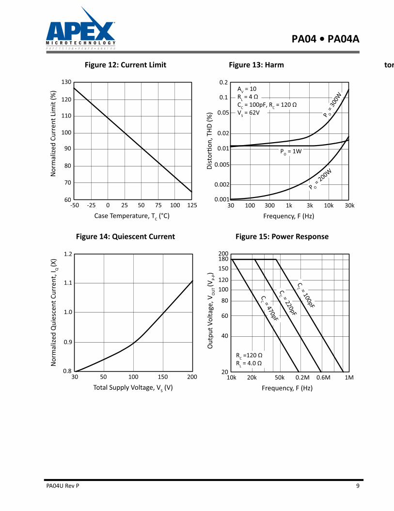
Figure 12: Current Limit
130
120
110
100
90
80
70
60-50 -25 25 50 75 125100
Case Temperature, TC (°C)
Nor
mal
ized
Curr
ent L
imit
(%)
0
Figure 13: Harmonic Distortion
0.2
0.1
0.05
0.02
0.01
0.005
0.002
0.00130 100 300 1k 3k 30k10k
Frequency, F (Hz))
AV = 10RLCC = 100pF, RCVS = 62V
P O = 200W
PO = 1W
P O =
300W
Figure 14: Quiescent Current
1.2
1.1
1.0
0.9
0.830 50 100 150 200
Total Supply Voltage, VS (V)
Nor
mal
ized
Qui
esce
nt C
urre
nt, I
Q (X
)
Figure 15: Power Response
200180150
120100
80
60
40
2010k 20k 50k 0.2M 1M0.6M
Frequency, F (Hz)
Out
put V
olta
ge, V
OU
T (V
P-P)
RCRL
CC = 220pF
CC = 100pF
CC = 470pF
PA04U Rev P 9
PA04 • PA04A
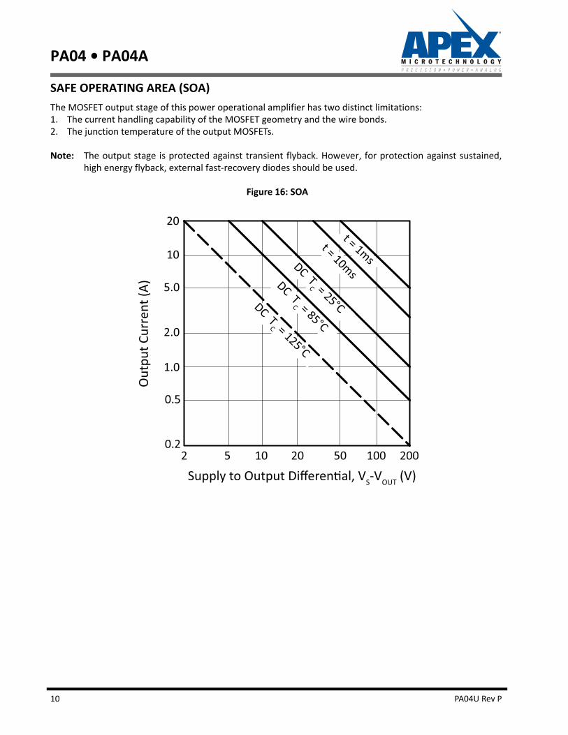
SAFE OPERATING AREA (SOA)
The MOSFET output stage of this power operational amplifier has two distinct limitations:1. The current handling capability of the MOSFET geometry and the wire bonds.2. The junction temperature of the output MOSFETs.
Note: The output stage is protected against transient flyback. However, for protection against sustained, high energy flyback, external fast-recovery diodes should be used.
Figure 16: SOA
20
10
5.0
2.0
1.0
0.5
0.22 5 10 20 50 200100
VS-VOUT (V)
)
DC TC = 125°C
DC TC = 85°C
DC TC = 25°C
t = 10ms
t = 1ms
10 PA04U Rev P

PA04 • PA04A
GENERAL
Please read Application Note 1 “General Operating Considerations” which covers stability, supplies, heat sinking, mounting, current limit, SOA interpretation, and specification interpretation. Visit www.apexana-log.com for Apex Microtechnology’s complete Application Notes library, Technical Seminar Workbook, and Evaluation Kits.
TYPICAL APPLICATION
Figure 17: Typical Application (Sonar Transducer Driver)
The high power bandwidth and high voltage output of the PA04 allows driving sonar transducers via a resonant circuit including the transducer and a matching transformer. The load circuit appears resistive to the PA04. Control logic turns off the amplifier in sleep mode.
PHASE COMPENSATION
Gain CC* RC
≥1 470pF 120 Ω
≥3 220pF 120 Ω
≥10 100pF 120 Ω
CC Rated For Full Supply Voltage
*See “BOOST OPERATION” paragraph.
PA04U Rev P 11

PA04 • PA04A
CURRENT LIMIT
The two current limit sense lines are to be connected directly across the current limit sense resistor. For the current limit to work correctly pin 11 must be connected to the amplifier output side and pin 10 con-nected to the load side of the current limit resistor, RCL, as shown in Figure 18. This connection will bypass
any parasitic resistances, RP, formed by sockets and solder joints as well as internal amplifier losses. The cur-
rent limiting resistor may not be placed anywhere in the output circuit except where shown in Figure 18.The value of the current limit resistor can be calculated as follows:
RCL 0.76VICL A -----------------=
Figure 18: Current Limit
12 PA04U Rev P

PA04 • PA04A
SLEEP MODE OPERATION
To activate sleep mode, connect pin 12 (sleep) to pin 9 (+VB). This disables the amplifier’s internal refer-
ence and the amplifier shuts down except for a trickle current of 3 mA which flows into pin 12. Pin 12 should be left open if the sleep mode is not required.
Several possible circuits can be built to take advantage of this mode. In Figure 19a a small signal relay is driven by a logic gate. This removes the requirement to deal with the common mode voltage that exists on the shutoff circuitry since the sleep mode is referenced to the +VB voltage.
In Figure 19b, circuitry is used to level translate the sleep mode input signal. The differential input acti-vates sleep mode with a differential logic level signal and allows common mode voltages to ±VB.
Figure 19: Sleep Mode Current
BOOST OPERATION
With the VB feature the small signal stages of the amplifier are operated at higher supply voltages than
the amplifier’s high current output stage. +VB (pin 9) and –VB (pin 5) are connected to the small signal cir-
cuitry of the amplifier. +VS (pin 8) and –VS (pin 6) are connected to the high current output stage. An addi-
tional 5V on the VB pins is sufficient to allow the small signal stages to drive the output transistors into
saturation and improve the output voltage swing for extra efficient operation when required. When close swings to the supply rails is not required the +VB and +VS pins must be strapped together as well as the
–VB and –VS pins. The VB pins must not be at a voltage lower than the VS pins.
COMPENSATION
The external compensation components CC and RC are connected to pins 3 and 4. Unity gain stability can
be achieved at any compensation capacitance greater than 330 pF with at least 60 degrees of phase margin. At higher gains more phase shift can be tolerated in most designs and the compensation capacitance can accordingly be reduced, resulting in higher bandwidth and slew rate. Use the typical operating curves as a guide to select CC and RC for the application.
PA04U Rev P 13

PA04 • PA04A
PACKAGE DESIGN
PACKAGE STYLE CR
PA04U Rev P 14
NEED TECHNICAL HELP? CONTACT APEX SUPPORT! For all Apex Microtechnology product questions and inquiries, call toll free 800-546-2739 in North America. For inquiries via email, please contact [email protected]. International customers can also request support by contacting their local Apex Microtechnology Sales Representative. To find the one nearest to you, go to www.apexanalog.com
IMPORTANT NOTICE
Apex Microtechnology, Inc. has made every effort to insure the accuracy of the content contained in this document. However, the information is
subject to change without notice and is provided "AS IS" without warranty of any kind (expressed or implied). Apex Microtechnology reserves the right
to make changes without further notice to any specifications or products mentioned herein to improve reliability. This document is the property of Apex Microtechnology and by furnishing this information, Apex Microtechnology grants no license, expressed or implied under any patents, mask
work rights, copyrights, trademarks, trade secrets or other intellectual property rights. Apex Microtechnology owns the copyrights associated with the
information contained herein and gives consent for copies to be made of the information only for use within your organization with respect to Apex Microtechnology integrated circuits or other products of Apex Microtechnology. This consent does not extend to other copying such as copying for
general distribution, advertising or promotional purposes, or for creating any work for resale.
APEX MICROTECHNOLOGY PRODUCTS ARE NOT DESIGNED, AUTHORIZED OR WARRANTED TO BE SUITABLE FOR USE IN PRODUCTS USED FOR LIFE SUPPORT, AUTOMOTIVE SAFETY, SECURITY DEVICES, OR OTHER CRITICAL APPLICATIONS. PRODUCTS IN SUCH APPLICATIONS ARE UNDERSTOOD TO BE
FULLY AT THE CUSTOMER OR THE CUSTOMER’S RISK.
Apex Microtechnology, Apex and Apex Precision Power are trademarks of Apex Microtechnology, Inc. All other corporate names noted herein may be trademarks of their respective holders.