P89LPC901/902/903 8-bit microcontrollers with two-clock ... · PDF filePhilips Semiconductors...
53
P89LPC901/902/903 8-bit microcontrollers with two-clock 80C51 core 1 kB 3 V Flash with 128-byte RAM Rev. 05 — 17 December 2004 Product data 1. General description The P89LPC901/902/903 are single-chip microcontrollers in low-cost 8-pin packages, based on a high performance processor architecture that executes instructions in two to four clocks, six times the rate of standard 80C51 devices. Many system-level functions have been incorporated into the P89LPC901/902/903 in order to reduce component count, board space, and system cost. 2. Features 2.1 Principal features ■ 1 kB byte-erasable Flash code memory organized into 256-byte sectors and 16-byte pages. Single-byte erasing allows any byte(s) to be used as non-volatile data storage. ■ 128-byte RAM data memory. ■ Two 16-bit counter/timers. (P89LPC901 Timer 0 may be configured to toggle a port output upon timer overflow or to become a PWM output.) ■ 23-bit system timer that can also be used as a Real-Time clock. ■ Two analog comparators (P89LPC902 and P89LPC903, single analog comparator on P89LPC901). ■ Enhanced UART with fractional baudrate generator, break detect, framing error detection, automatic address detection and versatile interrupt capabilities (P89LPC903). ■ High-accuracy internal RC oscillator option allows operation without external oscillator components. The RC oscillator (factory calibrated to ±1 %) option is selectable and fine tunable. ■ 2.4 V to 3.6 V V DD operating range with 5 V tolerant I/O pins (may be pulled up or driven to 5.5 V). Industry-standard pinout with V DD , V SS , and reset at locations 1, 8, and 4. ■ Up to six I/O pins when using internal oscillator and reset options. ■ 8-pin SO-8 package. 2.2 Additional features ■ A high performance 80C51 CPU provides instruction cycle times of 111 ns to 222 ns for all instructions except multiply and divide when executing at 18 MHz (167 ns to 333 ns at 12 MHz). This is six times the performance of the standard 80C51 running at the same clock frequency. A lower clock frequency for the same performance results in power savings and reduced EMI. ■ In-Application Programming (IAP-Lite) and byte erase allows code memory to be used for non-volatile data storage.
Transcript of P89LPC901/902/903 8-bit microcontrollers with two-clock ... · PDF filePhilips Semiconductors...

P89LPC901/902/9038-bit microcontrollers with two-clock 80C51 core1 kB 3 V Flash with 128-byte RAMRev. 05 — 17 December 2004 Product data
1. General description
The P89LPC901/902/903 are single-chip microcontrollers in low-cost 8-pin packages,based on a high performance processor architecture that executes instructions in twoto four clocks, six times the rate of standard 80C51 devices. Many system-levelfunctions have been incorporated into the P89LPC901/902/903 in order to reducecomponent count, board space, and system cost.
2. Features
2.1 Principal features 1 kB byte-erasable Flash code memory organized into 256-byte sectors and
16-byte pages. Single-byte erasing allows any byte(s) to be used as non-volatiledata storage.
128-byte RAM data memory.
Two 16-bit counter/timers. (P89LPC901 Timer 0 may be configured to toggle aport output upon timer overflow or to become a PWM output.)
23-bit system timer that can also be used as a Real-Time clock.
Two analog comparators (P89LPC902 and P89LPC903, single analogcomparator on P89LPC901).
Enhanced UART with fractional baudrate generator, break detect, framing errordetection, automatic address detection and versatile interrupt capabilities(P89LPC903).
High-accuracy internal RC oscillator option allows operation without externaloscillator components. The RC oscillator (factory calibrated to ±1 %) option isselectable and fine tunable.
2.4 V to 3.6 V VDD operating range with 5 V tolerant I/O pins (may be pulled up ordriven to 5.5 V). Industry-standard pinout with VDD, VSS, and reset at locations 1,8, and 4.
Up to six I/O pins when using internal oscillator and reset options.
8-pin SO-8 package.
2.2 Additional features A high performance 80C51 CPU provides instruction cycle times of 111 ns to
222 ns for all instructions except multiply and divide when executing at 18 MHz(167 ns to 333 ns at 12 MHz). This is six times the performance of the standard80C51 running at the same clock frequency. A lower clock frequency for the sameperformance results in power savings and reduced EMI.
In-Application Programming (IAP-Lite) and byte erase allows code memory to beused for non-volatile data storage.

Philips Semiconductors P89LPC901/902/9038-bit microcontrollers with two-clock 80C51 core
Serial Flash In-Circuit Programming (ICP) allows simple production coding withcommercial EPROM programmers. Flash security bits prevent reading of sensitiveapplication programs.
Watchdog timer with separate on-chip oscillator, requiring no externalcomponents. The watchdog prescaler is selectable from 8 values.
Low voltage reset (Brownout detect) allows a graceful system shutdown whenpower fails. May optionally be configured as an interrupt.
Idle and two different Power-down reduced power modes. Improved wake-up fromPower-down mode (a low interrupt input starts execution). Typical Power-downcurrent is 1 µA (total Power-down with voltage comparators disabled).
Active-LOW reset. On-chip power-on reset allows operation without external resetcomponents. A reset counter and reset glitch suppression circuitry preventspurious and incomplete resets. A software reset function is also available.
Configurable on-chip oscillator with frequency range options selected by userprogrammed Flash configuration bits. Oscillator options support frequencies from20 kHz to the maximum operating frequency of 18 MHz (P89LPC901).
Watchdog timer with separate on-chip oscillator, requiring no externalcomponents. The watchdog prescaler is selectable from 8 values.
Programmable port output configuration options: quasi-bidirectional, open drain,push-pull, input-only.
Port ‘input pattern match’ detect. Port 0 may generate an interrupt when the valueof the pins match or do not match a programmable pattern.
LED drive capability (20 mA) on all port pins. A maximum limit is specified for theentire chip.
Controlled slew rate port outputs to reduce EMI. Outputs have approximately10 ns minimum ramp times.
Only power and ground connections are required to operate theP89LPC901/902/903 when internal reset option is selected.
Four interrupt priority levels.
Two (P89LPC901), three (P89LPC903), or five (P89LPC902) keypad interruptinputs.
Second data pointer.
Schmitt trigger port inputs.
Emulation support.
Product data Rev. 05 — 17 December 2004 2 of 53
9397 750 14465 © Koninklijke Philips Electronics N.V. 2004. All rights reserved.

Philips Semiconductors P89LPC901/902/9038-bit microcontrollers with two-clock 80C51 core
3. Ordering information
3.1 Ordering options
Table 1: Ordering information
Type number Package
Name Description Version
P89LPC901FD SO8 plastic small outline package; 8 leads;body width 7.5 mm
SOT96-1
P89LPC902FD
P89LPC903FD
P89LPC901FN DIP8 plastic dual in-line package; 8 leads (300 mil) SOT97-1
P89LPC902FN
Table 2: Part options
Type number Temperature range Frequency
P89LPC901xx −40 °C to +85 °C 0 MHz to 18 MHz
P89LPC902xx Internal RC or watchdog
P89LPC903xx Internal RC or watchdog
Product data Rev. 05 — 17 December 2004 3 of 53
9397 750 14465 © Koninklijke Philips Electronics N.V. 2004. All rights reserved.

Philips Semiconductors P89LPC901/902/9038-bit microcontrollers with two-clock 80C51 core
4. Block diagram
Fig 1. P89LPC901 block diagram.
HIGH PERFORMANCEACCELERATED 2-CLOCK 80C51 CPU
1 kBCODE FLASH
128-BYTEDATA RAM
PORT 3CONFIGURABLE I/Os
PORT 0CONFIGURABLE I/Os
KEYPADINTERRUPT
PROGRAMMABLEOSCILLATOR DIVIDER
CPUCLOCK
CONFIGURABLEOSCILLATOR
ON-CHIPRC
OSCILLATOR
INTERNAL BUS
CRYSTALOR
RESONATOR
POWER MONITOR(POWER-ON RESET, BROWNOUT RESET)
002aaa444
REAL-TIME CLOCK/SYSTEM TIMER
TIMER 0TIMER 1
ANALOGCOMPARATOR
PORT 1CONFIGURABLE I/Os
WATCHDOG TIMERAND OSCILLATOR
P89LPC901
Product data Rev. 05 — 17 December 2004 4 of 53
9397 750 14465 © Koninklijke Philips Electronics N.V. 2004. All rights reserved.

Philips Semiconductors P89LPC901/902/9038-bit microcontrollers with two-clock 80C51 core
Fig 2. P89LPC902 block diagram.
HIGH PERFORMANCEACCELERATED 2-CLOCK 80C51 CPU
1 kBCODE FLASH
128-BYTEDATA RAM
PORT 0CONFIGURABLE I/Os
KEYPADINTERRUPT
PROGRAMMABLEOSCILLATOR DIVIDER CPU
CLOCK
ON-CHIPRC
OSCILLATOR
INTERNALBUS
POWER MONITOR(POWER-ON RESET, BROWNOUT RESET)
002aaa445
REAL-TIME CLOCK/SYSTEM TIMER
TIMER 0TIMER 1
ANALOGCOMPARATORS
PORT 1INPUT
WATCHDOG TIMERAND OSCILLATOR
P89LPC902
Product data Rev. 05 — 17 December 2004 5 of 53
9397 750 14465 © Koninklijke Philips Electronics N.V. 2004. All rights reserved.
Philips Semiconductors P89LPC901/902/9038-bit microcontrollers with two-clock 80C51 core
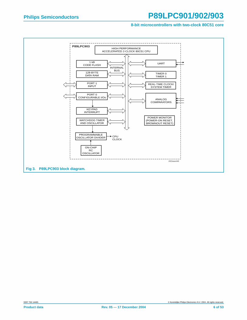
Fig 3. P89LPC903 block diagram.
HIGH PERFORMANCEACCELERATED 2-CLOCK 80C51 CPU
1 kBCODE FLASH
128-BYTEDATA RAM
PORT 0CONFIGURABLE I/Os
KEYPADINTERRUPT
PROGRAMMABLEOSCILLATOR DIVIDER CPU
CLOCK
ON-CHIPRC
OSCILLATOR
INTERNALBUS
POWER MONITOR(POWER-ON RESET, BROWNOUT RESET)
002aaa446
REAL-TIME CLOCK/SYSTEM TIMER
TIMER 0TIMER 1
UART
ANALOGCOMPARATORS
PORT 1INPUT
WATCHDOG TIMERAND OSCILLATOR
P89LPC903
Product data Rev. 05 — 17 December 2004 6 of 53
9397 750 14465 © Koninklijke Philips Electronics N.V. 2004. All rights reserved.
Philips Semiconductors P89LPC901/902/9038-bit microcontrollers with two-clock 80C51 core
5. Pinning information
5.1 Pinning
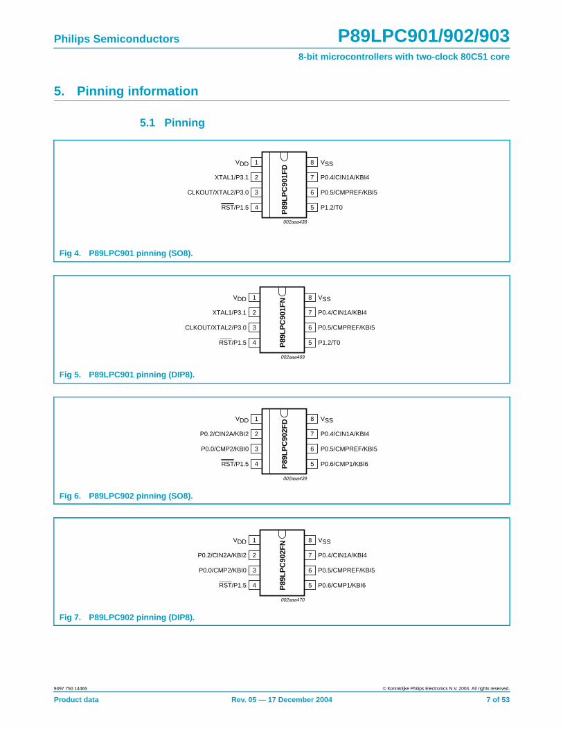
Fig 4. P89LPC901 pinning (SO8).
handbook, halfpage
002aaa438
P89
LPC
901F
D
1
2
3
4
8
7
6
5
VSS
P0.4/CIN1A/KBI4
P0.5/CMPREF/KBI5
P1.2/T0
VDD
XTAL1/P3.1
CLKOUT/XTAL2/P3.0
RST/P1.5
Fig 5. P89LPC901 pinning (DIP8).
handbook, halfpage
002aaa469
P89
LPC
901F
N1
2
3
4
VDD
XTAL1/P3.1
CLKOUT/XTAL2/P3.0
RST/P1.5
VSS
P0.4/CIN1A/KBI4
P0.5/CMPREF/KBI5
P1.2/T0
8
7
6
5
Fig 6. P89LPC902 pinning (SO8).
handbook, halfpage
002aaa439
P89
LPC
902F
D1
2
3
4
8
7
6
5
VSS
P0.4/CIN1A/KBI4
P0.5/CMPREF/KBI5
P0.6/CMP1/KBI6
VDD
P0.2/CIN2A/KBI2
P0.0/CMP2/KBI0
RST/P1.5
Fig 7. P89LPC902 pinning (DIP8).
handbook, halfpage
002aaa470
P89
LPC
902F
N1
2
3
4
VDD
P0.2/CIN2A/KBI2
P0.0/CMP2/KBI0
RST/P1.5
VSS
P0.4/CIN1A/KBI4
P0.5/CMPREF/KBI5
P0.6/CMP1/KBI6
8
7
6
5
Product data Rev. 05 — 17 December 2004 7 of 53
9397 750 14465 © Koninklijke Philips Electronics N.V. 2004. All rights reserved.

Philips Semiconductors P89LPC901/902/9038-bit microcontrollers with two-clock 80C51 core
5.2 Pin description
Fig 8. P89LPC903 pinning (SO8).
handbook, halfpage
002aaa440
P89
LPC
903F
D1
2
3
4
8
7
6
5
VSS
P0.4/CIN1A/KBI4
P0.5/CMPREF/KBI5
P1.0/TxD
VDD
P0.2/CIN2A/KBI2
P1.1/RxD
RST/P1.5
Table 3: P89LPC901 pin description
Symbol Pin Type Description
P0.0 to P0.6 I/O Port 0: Port 0 is an I/O port with a user-configurable output type. During reset Port 0latches are configured in the input only mode with the internal pull-up disabled. Theoperation of Port 0 pins as inputs and outputs depends upon the port configurationselected. Each port pin is configured independently. Refer to Section 8.12.1 “Portconfigurations” and Table 13 “DC electrical characteristics” for details.
The Keypad Interrupt feature operates with Port 0 pins.
All pins have Schmitt triggered inputs.
Port 0 also provides various special functions as described below:
7 I/O P0.4 — Port 0 bit 4.
I CIN1A — Comparator 1 positive input.
I KBI4 — Keyboard input 4.
6 I/O P0.5 — Port 0 bit 5.
I CMPREF — Comparator reference (negative) input.
I KBI5 — Keyboard input 5.
Product data Rev. 05 — 17 December 2004 8 of 53
9397 750 14465 © Koninklijke Philips Electronics N.V. 2004. All rights reserved.

Philips Semiconductors P89LPC901/902/9038-bit microcontrollers with two-clock 80C51 core
P1.0 to P1.5 Port 1: Port 1 is an I/O port with a user-configurable output type. During reset Port 1latches are configured in the input only mode with the internal pull-up disabled. Theoperation of the configurable Port 1 pins as inputs and outputs depends upon theport configuration selected. Each of the configurable port pins are programmedindependently. Refer to Section 8.12.1 “Port configurations” and Table 13 “DCelectrical characteristics” for details. P1.5 is input only.
All pins have Schmitt triggered inputs.
Port 1 also provides various special functions as described below:
5 I/O P1.2 — Port 1 bit 2.
O T0 — Timer/counter 0 external count input or overflow output.
4 I P1.5 — Port 1 bit 5 (input only).
I RST — External Reset input during Power-on or if selected via UCFG1. Whenfunctioning as a reset input a LOW on this pin resets the microcontroller, causing I/Oports and peripherals to take on their default states, and the processor beginsexecution at address 0. When using an oscillator frequency above 12 MHz, thereset input function of P1.5 must be enabled. An external circuit is required tohold the device in reset at power-up until V DD has reached its specified level.When system power is removed V DD will fall below the minimum specifiedoperating voltage. When using an oscillator frequency above 12 MHz, in someapplications, an external brownout detect circuit may be required to hold thedevice in reset when V DD falls below the minimum specified operating voltage.Also used during a power-on sequence to force In-System Programming mode.
P3.0 to P3.1 I/O Port 3: Port 3 is an I/O port with a user-configurable output types. During reset Port 3latches are configured in the input only mode with the internal pull-up disabled. Theoperation of port 3 pins as inputs and outputs depends upon the port configurationselected. Each port pin is configured independently. Refer to Section 8.12.1 “Portconfigurations” and Table 13 “DC electrical characteristics” for details.
All pins have Schmitt triggered inputs.
Port 3 also provides various special functions as described below:
3 I/O P3.0 — Port 3 bit 0.
O XTAL2 — Output from the oscillator amplifier (when a crystal oscillator option isselected via the FLASH configuration).
O CLKOUT — CPU clock divided by 2 when enabled via SFR bit (ENCLK to TRIM.6). Itcan be used if the CPU clock is the internal RC oscillator, Watchdog oscillator orexternal clock input, except when XTAL1/XTAL2 are used to generate clock sourcefor the real time clock/system timer.
2 I/O P3.1 — Port 3 bit 1.
I XTAL1 — Input to the oscillator circuit and internal clock generator circuits (whenselected via the FLASH configuration). It can be a port pin if internal RC oscillator orWatchdog oscillator is used as the CPU clock source, and if XTAL1/XTAL2 are notused to generate the clock for the real time clock/system timer.
VSS 8 I Ground: 0 V reference.
VDD 1 I Power Supply: This is the power supply voltage for normal operation as well as Idleand Power-down modes.
Table 3: P89LPC901 pin description …continued
Symbol Pin Type Description
Product data Rev. 05 — 17 December 2004 9 of 53
9397 750 14465 © Koninklijke Philips Electronics N.V. 2004. All rights reserved.

Philips Semiconductors P89LPC901/902/9038-bit microcontrollers with two-clock 80C51 core
Table 4: P89LPC902 pin description
Symbol Pin Type Description
P0.0 to P0.6 I/O Port 0: Port 0 is an I/O port with a user-configurable output type. During reset Port 0latches are configured in the input only mode with the internal pull-up disabled. Theoperation of Port 0 pins as inputs and outputs depends upon the port configurationselected. Each port pin is configured independently. Refer to Section 8.12.1 “Portconfigurations” and Table 13 “DC electrical characteristics” for details.
The Keypad Interrupt feature operates with Port 0 pins.
All pins have Schmitt triggered inputs.
Port 0 also provides various special functions as described below:
3 I/O P0.0 — Port 0 bit 0.
I CMP2 — Comparator 2 output.
I KBI0 — Keyboard input 0.
2 I/O P0.2 — Port 0 bit 2.
I CIN2A — Comparator 2 positive input.
I KBI2 — Keyboard input 2.
7 I/O P0.4 — Port 0 bit 4.
I CIN1A — Comparator 1 positive input.
I KBI4 — Keyboard input 4.
6 I/O P0.5 — Port 0 bit 5.
I CMPREF — Comparator reference (negative) input.
I KBI5 — Keyboard input 5.
5 I/O P0.6 — Port 0 bit 6.
O CMP1 — Comparator 1 output.
I KBI6 — Keyboard input 6.
P1.0 to P1.5 Port 1: Port 1 is an I/O port with a user-configurable output type. During reset Port 1latches are configured in the input only mode with the internal pull-up disabled. Theoperation of the configurable Port 1 pins as inputs and outputs depends upon theport configuration selected. Each of the configurable port pins are programmedindependently. Refer to Section 8.12.1 “Port configurations” and Table 13 “DCelectrical characteristics” for details. P1.5 is input only.
All pins have Schmitt triggered inputs.
Port 1 also provides various special functions as described below:
4 I P1.5 — Port 1 bit 5 (input only).
I RST — External Reset input during Power-on or if selected via UCFG1. Whenfunctioning as a reset input a LOW on this pin resets the microcontroller, causing I/Oports and peripherals to take on their default states, and the processor beginsexecution at address 0. Also used during a power-on sequence to force In-SystemProgramming mode.
VSS 8 I Ground: 0 V reference.
VDD 1 I Power Supply: This is the power supply voltage for normal operation as well as Idleand Power-down modes.
Product data Rev. 05 — 17 December 2004 10 of 53
9397 750 14465 © Koninklijke Philips Electronics N.V. 2004. All rights reserved.
Philips Semiconductors P89LPC901/902/9038-bit microcontrollers with two-clock 80C51 core
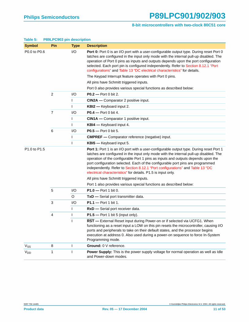
Table 5: P89LPC903 pin description
Symbol Pin Type Description
P0.0 to P0.6 I/O Port 0: Port 0 is an I/O port with a user-configurable output type. During reset Port 0latches are configured in the input only mode with the internal pull-up disabled. Theoperation of Port 0 pins as inputs and outputs depends upon the port configurationselected. Each port pin is configured independently. Refer to Section 8.12.1 “Portconfigurations” and Table 13 “DC electrical characteristics” for details.
The Keypad Interrupt feature operates with Port 0 pins.
All pins have Schmitt triggered inputs.
Port 0 also provides various special functions as described below:
2 I/O P0.2 — Port 0 bit 2.
I CIN2A — Comparator 2 positive input.
I KBI2 — Keyboard input 2.
7 I/O P0.4 — Port 0 bit 4.
I CIN1A — Comparator 1 positive input.
I KBI4 — Keyboard input 4.
6 I/O P0.5 — Port 0 bit 5.
I CMPREF — Comparator reference (negative) input.
I KBI5 — Keyboard input 5.
P1.0 to P1.5 Port 1: Port 1 is an I/O port with a user-configurable output type. During reset Port 1latches are configured in the input only mode with the internal pull-up disabled. Theoperation of the configurable Port 1 pins as inputs and outputs depends upon theport configuration selected. Each of the configurable port pins are programmedindependently. Refer to Section 8.12.1 “Port configurations” and Table 13 “DCelectrical characteristics” for details. P1.5 is input only.
All pins have Schmitt triggered inputs.
Port 1 also provides various special functions as described below:
5 I/O P1.0 — Port 1 bit 0.
O TxD — Serial port transmitter data.
3 I/O P1.1 — Port 1 bit 1.
I RxD — Serial port receiver data.
4 I P1.5 — Port 1 bit 5 (input only).
I RST — External Reset input during Power-on or if selected via UCFG1. Whenfunctioning as a reset input a LOW on this pin resets the microcontroller, causing I/Oports and peripherals to take on their default states, and the processor beginsexecution at address 0. Also used during a power-on sequence to force In-SystemProgramming mode.
VSS 8 I Ground: 0 V reference.
VDD 1 I Power Supply: This is the power supply voltage for normal operation as well as Idleand Power-down modes.
Product data Rev. 05 — 17 December 2004 11 of 53
9397 750 14465 © Koninklijke Philips Electronics N.V. 2004. All rights reserved.

Philips Semiconductors P89LPC901/902/9038-bit microcontrollers with two-clock 80C51 core
6. Logic symbols
Fig 9. P89LPC901 logic symbol.
VDD VSS
P89
LPC
901
PO
RT
0P
OR
T 3
PO
RT
1
T0RST
002aaa441
CIN1ACMPREF
XTAL2
XTAL1
KBI4KBI5
CLKOUT
Fig 10. P89LPC902 logic symbol.
VDD VSS
P89
LPC
902
PO
RT
0
PO
RT
1
RST
002aaa442
CIN1ACMPREF
CMP1CIN2ACMP2
KBI4KBI5KBI6KBI2KBI0
Fig 11. P89LPC903 logic symbol.
VDD VSS
P89
LPC
903
PO
RT
0
PO
RT
1 RSTRxDTxD
002aaa443
CIN1ACMPREF
CIN2A
KBI4KBI5KBI2
Product data Rev. 05 — 17 December 2004 12 of 53
9397 750 14465 © Koninklijke Philips Electronics N.V. 2004. All rights reserved.

Philips Semiconductors P89LPC901/902/9038-bit microcontrollers with two-clock 80C51 core
Table 6 highlights the differences between these three devices. For a complete list ofdevice features, please see Section 2 “Features” on page 1.
Table 6: Product comparison overview
Type number Externalcrystal pins
CLKOUT output T0 PWM output CMP2 input CMP1 andCMP2 outputs
UART
TxD Rxd
P89LPC901xx X X X - - - -
P89LPC902xx - - - X X - -
P89LPC903xx - - - X - X X
Product data Rev. 05 — 17 December 2004 13 of 53
9397 750 14465 © Koninklijke Philips Electronics N.V. 2004. All rights reserved.

Philips Semiconductors P89LPC901/902/9038-bit microcontrollers with two-clock 80C51 core
7. Special function registers
Remark: Special Function Registers (SFRs) accesses are restricted in the followingways:
• User must not attempt to access any SFR locations not defined.
• Accesses to any defined SFR locations must be strictly for the functions for theSFRs.
• SFR bits labeled ‘-’, ‘0’ or ‘1’ can only be written and read as follows:
– ‘-’ Unless otherwise specified, must be written with ‘0’, but can return any valuewhen read (even if it was written with ‘0’). It is a reserved bit and may be used infuture derivatives.
– ‘0’ must be written with ‘0’, and will return a ‘0’ when read.
– ‘1’ must be written with ‘1’, and will return a ‘1’ when read.
Product data Rev. 05 — 17 December 2004 14 of 53
9397 750 14465 © Koninklijke Philips Electronics N.V. 2004. All rights reserved.
xxxxxxxxxxxxxxxxxxxxx xxxxxxxxxxxxxxxxxxxxxxxxxx xxxxxxx x x x xxxxxxxxxxxxxxxxxxxxxxxxxxxxxx xxxxxxxxxxxxxxxxxxx xx xxxxxxx xxxxxxxxxxxxxxxxxxxxxxxxxxx xxxxxxxxxxxxxxxxxxx xxxxxx xxxxxxxxxxxxxxxxxxxxxxxxxxxxxxxxxxx xxxxxxxxxxxx x xxxxxxxxxxxxxxxxxxxxxx xxxxxxxxxxxxxxxxxxxxxxxxxxxxxx xxxxx xxxxxxxxxxxxxxxxxxxxxxxxxxxxxxxxxxxxxxxxxxxxxxxxxx xxxxxxxxxxxxxxxxxxxxxxxxxxxxxxxxx xxxxxxxxxxxxxxxxxxxx xxx P
hilips Sem
iconductorsP
89LPC
901/902/9038-bit m
icrocontrollers with tw
o-clock 80C51 core
9397 750 14465©
Koninklijke P
hilips Electronics N
.V. 2004. All rights reserved.
Product data
Rev. 05 —
17 Decem
ber 200415 of 53
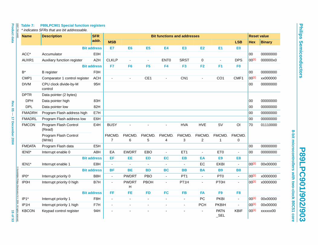
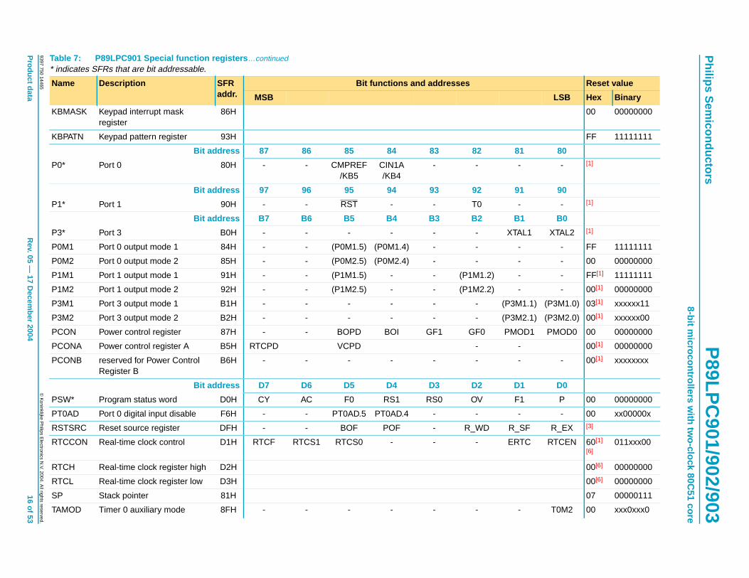
Table 7: P89LPC901 Special function registers* indicates SFRs that are bit addressable.
Reset value
LSB Hex Binary
E0
00 00000000
DPS 00[1] 000000x0
F0
00 00000000
CMF1 00[1] xx000000
00 00000000
00 00000000
00 00000000
00 00000000
00 00000000
OI 70 01110000
. FMCMD.0
00 00000000
- 00 00000000
E8
- 00[1] 00x00000
B8
- 00[1] x0000000
- 00[1] x0000000
F8
- 00[1] 00x00000
- 00[1] 00x00000
KBIF 00[1] xxxxxx00
Name Description SFRaddr.
Bit functions and addresses
MSB
Bit address E7 E6 E5 E4 E3 E2 E1
ACC* Accumulator E0H
AUXR1 Auxiliary function register A2H CLKLP - - ENT0 SRST 0 -
Bit address F7 F6 F5 F4 F3 F2 F1
B* B register F0H
CMP1 Comparator 1 control register ACH - - CE1 - CN1 - CO1
DIVM CPU clock divide-by-Mcontrol
95H
DPTR Data pointer (2 bytes)
DPH Data pointer high 83H
DPL Data pointer low 82H
FMADRH Program Flash address high E7H
FMADRL Program Flash address low E6H
FMCON Program Flash Control(Read)
E4H BUSY - - - HVA HVE SV
Program Flash Control(Write)
FMCMD.7
FMCMD.6
FMCMD.5
FMCMD.4
FMCMD.3
FMCMD.2
FMCMD1
FMDATA Program Flash data E5H
IEN0* Interrupt enable 0 A8H EA EWDRT EBO - ET1 - ET0
Bit address EF EE ED EC EB EA E9
IEN1* Interrupt enable 1 E8H - - - - - EC EKBI
Bit address BF BE BD BC BB BA B9
IP0* Interrupt priority 0 B8H - PWDRT PBO - PT1 - PT0
IP0H Interrupt priority 0 high B7H - PWDRTH
PBOH - PT1H - PT0H
Bit address FF FE FD FC FB FA F9
IP1* Interrupt priority 1 F8H - - - - - PC PKBI
IP1H Interrupt priority 1 high F7H - - - - - PCH PKBIH
KBCON Keypad control register 94H - - - - - - PATN_SEL
xxxxxxxxxxxxxxxxxxxxx xxxxxxxxxxxxxxxxxxxxxxxxxx xxxxxxx x x x xxxxxxxxxxxxxxxxxxxxxxxxxxxxxx xxxxxxxxxxxxxxxxxxx xx xxxxxxx xxxxxxxxxxxxxxxxxxxxxxxxxxx xxxxxxxxxxxxxxxxxxx xxxxxx xxxxxxxxxxxxxxxxxxxxxxxxxxxxxxxxxxx xxxxxxxxxxxx x xxxxxxxxxxxxxxxxxxxxxx xxxxxxxxxxxxxxxxxxxxxxxxxxxxxx xxxxx xxxxxxxxxxxxxxxxxxxxxxxxxxxxxxxxxxxxxxxxxxxxxxxxxx xxxxxxxxxxxxxxxxxxxxxxxxxxxxxxxxx xxxxxxxxxxxxxxxxxxxx xxx P
hilips Sem
iconductorsP
89LPC
901/902/9038-bit m
icrocontrollers with tw
o-clock 80C51 core
9397 750 14465©
Koninklijke P
hilips Electronics N
.V. 2004. All rights reserved.
Product data
Rev. 05 —
17 Decem
ber 200416 of 53
00 00000000
FF 11111111
80
- [1]
90
- [1]
B0
XTAL2 [1]
- FF 11111111
- 00 00000000
- FF[1] 11111111
- 00[1] 00000000
) (P3M1.0) 03[1] xxxxxx11
) (P3M2.0) 00[1] xxxxxx00
PMOD0 00 00000000
00[1] 00000000
- 00[1] xxxxxxxx
D0
P 00 00000000
- 00 xx00000x
R_EX [3]
RTCEN 60[1]
[6]011xxx00
00[6] 00000000
00[6] 00000000
07 00000111
T0M2 00 xxx0xxx0
Table 7: P89LPC901 Special function registers …continued* indicates SFRs that are bit addressable.
Reset value
LSB Hex Binary
KBMASK Keypad interrupt maskregister
86H
KBPATN Keypad pattern register 93H
Bit address 87 86 85 84 83 82 81
P0* Port 0 80H - - CMPREF/KB5
CIN1A/KB4
- - -
Bit address 97 96 95 94 93 92 91
P1* Port 1 90H - - RST - - T0 -
Bit address B7 B6 B5 B4 B3 B2 B1
P3* Port 3 B0H - - - - - - XTAL1
P0M1 Port 0 output mode 1 84H - - (P0M1.5) (P0M1.4) - - -
P0M2 Port 0 output mode 2 85H - - (P0M2.5) (P0M2.4) - - -
P1M1 Port 1 output mode 1 91H - - (P1M1.5) - - (P1M1.2) -
P1M2 Port 1 output mode 2 92H - - (P1M2.5) - - (P1M2.2) -
P3M1 Port 3 output mode 1 B1H - - - - - - (P3M1.1
P3M2 Port 3 output mode 2 B2H - - - - - - (P3M2.1
PCON Power control register 87H - - BOPD BOI GF1 GF0 PMOD1
PCONA Power control register A B5H RTCPD VCPD - -
PCONB reserved for Power ControlRegister B
B6H - - - - - - -
Bit address D7 D6 D5 D4 D3 D2 D1
PSW* Program status word D0H CY AC F0 RS1 RS0 OV F1
PT0AD Port 0 digital input disable F6H - - PT0AD.5 PT0AD.4 - - -
RSTSRC Reset source register DFH - - BOF POF - R_WD R_SF
RTCCON Real-time clock control D1H RTCF RTCS1 RTCS0 - - - ERTC
RTCH Real-time clock register high D2H
RTCL Real-time clock register low D3H
SP Stack pointer 81H
TAMOD Timer 0 auxiliary mode 8FH - - - - - - -
Name Description SFRaddr.
Bit functions and addresses
MSB

xxxxxxxxxxxxxxxxxxxxx xxxxxxxxxxxxxxxxxxxxxxxxxx xxxxxxx x x x xxxxxxxxxxxxxxxxxxxxxxxxxxxxxx xxxxxxxxxxxxxxxxxxx xx xxxxxxx xxxxxxxxxxxxxxxxxxxxxxxxxxx xxxxxxxxxxxxxxxxxxx xxxxxx xxxxxxxxxxxxxxxxxxxxxxxxxxxxxxxxxxx xxxxxxxxxxxx x xxxxxxxxxxxxxxxxxxxxxx xxxxxxxxxxxxxxxxxxxxxxxxxxxxxx xxxxx xxxxxxxxxxxxxxxxxxxxxxxxxxxxxxxxxxxxxxxxxxxxxxxxxx xxxxxxxxxxxxxxxxxxxxxxxxxxxxxxxxx xxxxxxxxxxxxxxxxxxxx xxx P
hilips Sem
iconductorsP
89LPC
901/902/9038-bit m
icrocontrollers with tw
o-clock 80C51 core
9397 750 14465©
Koninklijke P
hilips Electronics N
.V. 2004. All rights reserved.
Product data
Rev. 05 —
17 Decem
ber 200417 of 53
ince they may be used for other
POF and BOF; the power-on reset
after power-on reset. Other resets will
ister.
88
- 00 00000000
00 00000000
00 00000000
00 00000000
00 00000000
T0M0 00 00000000
TRIM.0 [5] [6]
WDCLK [4] [6]
FF 11111111
Table 7: P89LPC901 Special function registers …continued* indicates SFRs that are bit addressable.
Reset value
LSB Hex Binary
[1] All ports are in input only (high impedance) state after power-up.
[2] BRGR1 and BRGR0 must only be written if BRGEN in BRGCON SFR is ‘0’. If any are written while BRGEN = 1, the result is unpredictable.
Unimplemented bits in SFRs (labeled ’-’) are X (unknown) at all times. Unless otherwise specified, ones should not be written to these bits spurposes in future derivatives. The reset values shown for these bits are ‘0’s although they are unknown when read.
[3] The RSTSRC register reflects the cause of the P89LPC901/902/903 reset. Upon a power-up reset, all reset source flags are cleared exceptvalue is xx110000.
[4] After reset, the value is 111001x1, i.e., PRE2-PRE0 are all ‘1’, WDRUN = 1 and WDCLK = 1. WDTOF bit is ‘1’ after Watchdog reset and is ‘0’not affect WDTOF.
[5] On power-on reset, the TRIM SFR is initialized with a factory preprogrammed value. Other resets will not cause initialization of the TRIM reg
[6] The only reset source that affects these SFRs is power-on reset.
Bit address 8F 8E 8D 8C 8B 8A 89
TCON* Timer 0 and 1 control 88H TF1 TR1 TF0 TR0 - - -
TH0 Timer 0 high 8CH
TH1 Timer 1 high 8DH
TL0 Timer 0 low 8AH
TL1 Timer 1 low 8BH
TMOD Timer 0 and 1 mode 89H - - T1M1 T1M0 - - T0M1
TRIM Internal oscillator trim register 96H - - TRIM.5 TRIM.4 TRIM.3 TRIM.2 TRIM.1
WDCON Watchdog control register A7H PRE2 PRE1 PRE0 - - WDRUN WDTOF
WDL Watchdog load C1H
WFEED1 Watchdog feed 1 C2H
WFEED2 Watchdog feed 2 C3H
Name Description SFRaddr.
Bit functions and addresses
MSB

xxxxxxxxxxxxxxxxxxxxx xxxxxxxxxxxxxxxxxxxxxxxxxx xxxxxxx x x x xxxxxxxxxxxxxxxxxxxxxxxxxxxxxx xxxxxxxxxxxxxxxxxxx xx xxxxxxx xxxxxxxxxxxxxxxxxxxxxxxxxxx xxxxxxxxxxxxxxxxxxx xxxxxx xxxxxxxxxxxxxxxxxxxxxxxxxxxxxxxxxxx xxxxxxxxxxxx x xxxxxxxxxxxxxxxxxxxxxx xxxxxxxxxxxxxxxxxxxxxxxxxxxxxx xxxxx xxxxxxxxxxxxxxxxxxxxxxxxxxxxxxxxxxxxxxxxxxxxxxxxxx xxxxxxxxxxxxxxxxxxxxxxxxxxxxxxxxx xxxxxxxxxxxxxxxxxxxx xxx P
hilips Sem
iconductorsP
89LPC
901/902/9038-bit m
icrocontrollers with tw
o-clock 80C51 core
9397 750 14465©
Koninklijke P
hilips Electronics N
.V. 2004. All rights reserved.
Product data
Rev. 05 —
17 Decem
ber 200418 of 53
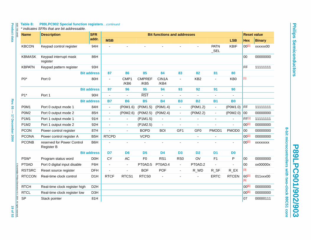
Table 8: P89LPC902 Special function registers* indicates SFRs that are bit addressable.
Reset value
LSB Hex Binary
E0
00 00000000
DPS 00[1] 000000x0
F0
00 00000000
CMF1 00[1] xx000000
CMF2 00[1] xx000000
00 00000000
00 00000000
00 00000000
00 00000000
00 00000000
OI 70 01110000
. FMCMD.0
00 00000000
- 00 00000000
E8
- 00[1] 00x00000
B8
- 00[1] x0000000
- 00[1] x0000000
F8
- 00[1] 00x00000
- 00[1] 00x00000
Name Description SFRaddr.
Bit functions and addresses
MSB
Bit address E7 E6 E5 E4 E3 E2 E1
ACC* Accumulator E0H
AUXR1 Auxiliary function register A2H - - - - SRST 0 -
Bit address F7 F6 F5 F4 F3 F2 F1
B* B register F0H
CMP1 Comparator 1 control register ACH - - CE1 - CN1 OE1 CO1
CMP2 Comparator 2 control register ADH - - CE2 - CN2 OE2 CO2
DIVM CPU clock divide-by-Mcontrol
95H
DPTR Data pointer (2 bytes)
DPH Data pointer high 83H
DPL Data pointer low 82H
FMADRH Program Flash address high E7H
FMADRL Program Flash address low E6H
FMCON Program Flash Control(Read)
E4H BUSY - - - HVA HVE SV
Program Flash Control(Write)
FMCMD.7
FMCMD.6
FMCMD.5
FMCMD.4
FMCMD.3
FMCMD.2
FMCMD1
FMDATA Program Flash data E5H
IEN0* Interrupt enable 0 A8H EA EWDRT EBO - ET1 - ET0
Bit address EF EE ED EC EB EA E9
IEN1* Interrupt enable 1 E8H - - - - - EC EKBI
Bit address BF BE BD BC BB BA B9
IP0* Interrupt priority 0 B8H - PWDRT PBO - PT1 - PT0
IP0H Interrupt priority 0 high B7H - PWDRTH
PBOH - PT1H - PT0H
Bit address FF FE FD FC FB FA F9
IP1* Interrupt priority 1 F8H - - - - - PC PKBI
IP1H Interrupt priority 1 high F7H - - - - - PCH PKBIH
xxxxxxxxxxxxxxxxxxxxx xxxxxxxxxxxxxxxxxxxxxxxxxx xxxxxxx x x x xxxxxxxxxxxxxxxxxxxxxxxxxxxxxx xxxxxxxxxxxxxxxxxxx xx xxxxxxx xxxxxxxxxxxxxxxxxxxxxxxxxxx xxxxxxxxxxxxxxxxxxx xxxxxx xxxxxxxxxxxxxxxxxxxxxxxxxxxxxxxxxxx xxxxxxxxxxxx x xxxxxxxxxxxxxxxxxxxxxx xxxxxxxxxxxxxxxxxxxxxxxxxxxxxx xxxxx xxxxxxxxxxxxxxxxxxxxxxxxxxxxxxxxxxxxxxxxxxxxxxxxxx xxxxxxxxxxxxxxxxxxxxxxxxxxxxxxxxx xxxxxxxxxxxxxxxxxxxx xxx P
hilips Sem
iconductorsP
89LPC
901/902/9038-bit m
icrocontrollers with tw
o-clock 80C51 core
9397 750 14465©
Koninklijke P
hilips Electronics N
.V. 2004. All rights reserved.
Product data
Rev. 05 —
17 Decem
ber 200419 of 53
KBIF 00[1] xxxxxx00
00 00000000
FF 11111111
80
KB0 [1]
90
-
B0
(P0M1.0) FF 11111111
(P0M2.0) 00 00000000
- FF[1] 11111111
- 00[1] 00000000
PMOD0 00 00000000
00[1] 00000000
- 00[1] xxxxxxxx
D0
P 00 00000000
- 00 xx00000x
R_EX [3]
RTCEN 60[1]
[6]011xxx00
00[6] 00000000
00[6] 00000000
07 00000111
Table 8: P89LPC902 Special function registers …continued* indicates SFRs that are bit addressable.
Reset value
LSB Hex Binary
KBCON Keypad control register 94H - - - - - - PATN_SEL
KBMASK Keypad interrupt maskregister
86H
KBPATN Keypad pattern register 93H
Bit address 87 86 85 84 83 82 81
P0* Port 0 80H - CMP1/KB6
CMPREF/KB5
CIN1A/KB4
- KB2 -
Bit address 97 96 95 94 93 92 91
P1* Port 1 90H - - RST - - - -
Bit address B7 B6 B5 B4 B3 B2 B1
P0M1 Port 0 output mode 1 84H - (P0M1.6) (P0M1.5) (P0M1.4) - (P0M1.2) -
P0M2 Port 0 output mode 2 85H - (P0M2.6) (P0M2.5) (P0M2.4) - (P0M2.2) -
P1M1 Port 1 output mode 1 91H - - (P1M1.5) - - - -
P1M2 Port 1 output mode 2 92H - - (P1M2.5) - - - -
PCON Power control register 87H - - BOPD BOI GF1 GF0 PMOD1
PCONA Power control register A B5H RTCPD VCPD - -
PCONB reserved for Power ControlRegister B
B6H - - - - - - -
Bit address D7 D6 D5 D4 D3 D2 D1
PSW* Program status word D0H CY AC F0 RS1 RS0 OV F1
PT0AD Port 0 digital input disable F6H - - PT0AD.5 PT0AD.4 - PT0AD.2 -
RSTSRC Reset source register DFH - - BOF POF - R_WD R_SF
RTCCON Real-time clock control D1H RTCF RTCS1 RTCS0 - - - ERTC
RTCH Real-time clock register high D2H
RTCL Real-time clock register low D3H
SP Stack pointer 81H
Name Description SFRaddr.
Bit functions and addresses
MSB

xxxxxxxxxxxxxxxxxxxxx xxxxxxxxxxxxxxxxxxxxxxxxxx xxxxxxx x x x xxxxxxxxxxxxxxxxxxxxxxxxxxxxxx xxxxxxxxxxxxxxxxxxx xx xxxxxxx xxxxxxxxxxxxxxxxxxxxxxxxxxx xxxxxxxxxxxxxxxxxxx xxxxxx xxxxxxxxxxxxxxxxxxxxxxxxxxxxxxxxxxx xxxxxxxxxxxx x xxxxxxxxxxxxxxxxxxxxxx xxxxxxxxxxxxxxxxxxxxxxxxxxxxxx xxxxx xxxxxxxxxxxxxxxxxxxxxxxxxxxxxxxxxxxxxxxxxxxxxxxxxx xxxxxxxxxxxxxxxxxxxxxxxxxxxxxxxxx xxxxxxxxxxxxxxxxxxxx xxx P
hilips Sem
iconductorsP
89LPC
901/902/9038-bit m
icrocontrollers with tw
o-clock 80C51 core
9397 750 14465©
Koninklijke P
hilips Electronics N
.V. 2004. All rights reserved.
Product data
Rev. 05 —
17 Decem
ber 200420 of 53
ince they may be used for other
POF and BOF; the power-on reset
after power-on reset. Other resets will
ister.
88
- 00 00000000
00 00000000
00 00000000
00 00000000
00 00000000
T0M0 00 00000000
TRIM.0 [5] [6]
WDCLK [4] [6]
FF 11111111
Table 8: P89LPC902 Special function registers …continued* indicates SFRs that are bit addressable.
Reset value
LSB Hex Binary
[1] All ports are in input only (high impedance) state after power-up.
[2] BRGR1 and BRGR0 must only be written if BRGEN in BRGCON SFR is ‘0’. If any are written while BRGEN = 1, the result is unpredictable.
Unimplemented bits in SFRs (labeled ’-’) are X (unknown) at all times. Unless otherwise specified, ones should not be written to these bits spurposes in future derivatives. The reset values shown for these bits are ‘0’s although they are unknown when read.
[3] The RSTSRC register reflects the cause of the P89LPC901/902/903 reset. Upon a power-up reset, all reset source flags are cleared exceptvalue is xx110000.
[4] After reset, the value is 111001x1, i.e., PRE2-PRE0 are all ‘1’, WDRUN = 1 and WDCLK = 1. WDTOF bit is ‘1’ after Watchdog reset and is ‘0’not affect WDTOF.
[5] On power-on reset, the TRIM SFR is initialized with a factory preprogrammed value. Other resets will not cause initialization of the TRIM reg
[6] The only reset source that affects these SFRs is power-on reset.
Bit address 8F 8E 8D 8C 8B 8A 89
TCON* Timer 0 and 1 control 88H TF1 TR1 TF0 TR0 - - -
TH0 Timer 0 high 8CH
TH1 Timer 1 high 8DH
TL0 Timer 0 low 8AH
TL1 Timer 1 low 8BH
TMOD Timer 0 and 1 mode 89H - - T1M1 T1M0 - - T0M1
TRIM Internal oscillator trim register 96H - - TRIM.5 TRIM.4 TRIM.3 TRIM.2 TRIM.1
WDCON Watchdog control register A7H PRE2 PRE1 PRE0 - - WDRUN WDTOF
WDL Watchdog load C1H
WFEED1 Watchdog feed 1 C2H
WFEED2 Watchdog feed 2 C3H
Name Description SFRaddr.
Bit functions and addresses
MSB

xxxxxxxxxxxxxxxxxxxxx xxxxxxxxxxxxxxxxxxxxxxxxxx xxxxxxx x x x xxxxxxxxxxxxxxxxxxxxxxxxxxxxxx xxxxxxxxxxxxxxxxxxx xx xxxxxxx xxxxxxxxxxxxxxxxxxxxxxxxxxx xxxxxxxxxxxxxxxxxxx xxxxxx xxxxxxxxxxxxxxxxxxxxxxxxxxxxxxxxxxx xxxxxxxxxxxx x xxxxxxxxxxxxxxxxxxxxxx xxxxxxxxxxxxxxxxxxxxxxxxxxxxxx xxxxx xxxxxxxxxxxxxxxxxxxxxxxxxxxxxxxxxxxxxxxxxxxxxxxxxx xxxxxxxxxxxxxxxxxxxxxxxxxxxxxxxxx xxxxxxxxxxxxxxxxxxxx xxx P
hilips Sem
iconductorsP
89LPC
901/902/9038-bit m
icrocontrollers with tw
o-clock 80C51 core
9397 750 14465©
Koninklijke P
hilips Electronics N
.V. 2004. All rights reserved.
Product data
Rev. 05 —
17 Decem
ber 200421 of 53
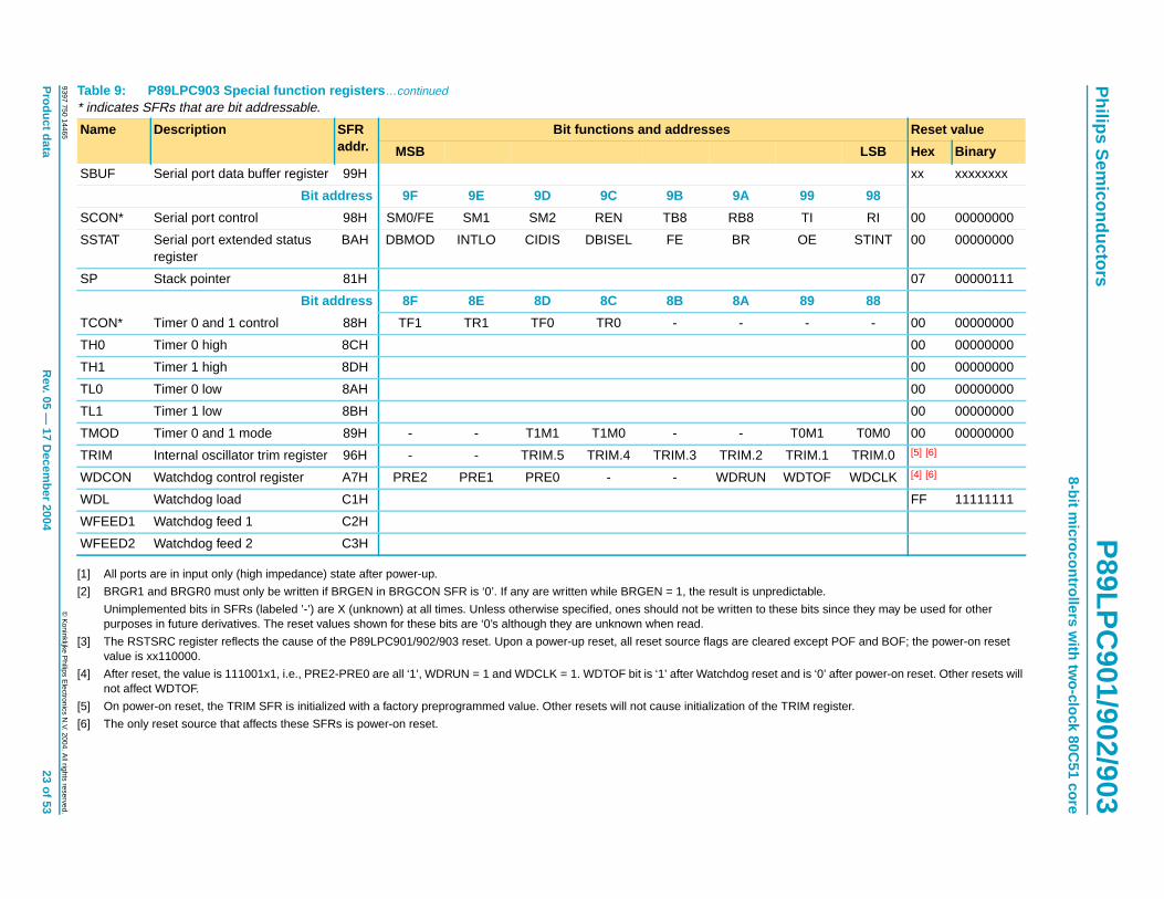
Table 9: P89LPC903 Special function registers* indicates SFRs that are bit addressable.
Reset value
LSB Hex Binary
E0
00 00000000
DPS 00[1] 000000x0
F0
00 00000000
00 00000000
00 00000000
BRGEN 00[6] xxxxxx00
CMF1 00[1] xx000000
CMF2 00[1] xx000000
00 00000000
00 00000000
00 00000000
00 00000000
00 00000000
OI 70 01110000
. FMCMD.0
00 00000000
- 00 00000000
E8
- 00[1] 00x00000
B8
- 00[1] x0000000
- 00[1] x0000000
F8
Name Description SFRaddr.
Bit functions and addresses
MSB
Bit address E7 E6 E5 E4 E3 E2 E1
ACC* Accumulator E0H
AUXR1 Auxiliary function register A2H - EBRR - - SRST 0 -
Bit address F7 F6 F5 F4 F3 F2 F1
B* B register F0H
BRGR0[2] Baud rate generator rate low BEH
BRGR1[2] Baud rate generator rate high BFH
BRGCON Baud rate generator control BDH - - - - - - SBRGS
CMP1 Comparator 1 control register ACH - - CE1 - CN1 - CO1
CMP2 Comparator 2 control register ADH - - CE2 - CN2 - CO2
DIVM CPU clock divide-by-Mcontrol
95H
DPTR Data pointer (2 bytes)
DPH Data pointer high 83H
DPL Data pointer low 82H
FMADRH Program Flash address high E7H
FMADRL Program Flash address low E6H
FMCON Program Flash Control(Read)
E4H BUSY - - - HVA HVE SV
Program Flash Control(Write)
FMCMD.7
FMCMD.6
FMCMD.5
FMCMD.4
FMCMD.3
FMCMD.2
FMCMD1
FMDATA Program Flash data E5H
IEN0* Interrupt enable 0 A8H EA EWDRT EBO ES/ESR ET1 - ET0
Bit address EF EE ED EC EB EA E9
IEN1* Interrupt enable 1 E8H - EST - - - EC EKBI
Bit address BF BE BD BC BB BA B9
IP0* Interrupt priority 0 B8H - PWDRT PBO PS/PSR PT1 - PT0
IP0H Interrupt priority 0 high B7H - PWDRTH
PBOH PSH/PSRH
PT1H - PT0H
Bit address FF FE FD FC FB FA F9

xxxxxxxxxxxxxxxxxxxxx xxxxxxxxxxxxxxxxxxxxxxxxxx xxxxxxx x x x xxxxxxxxxxxxxxxxxxxxxxxxxxxxxx xxxxxxxxxxxxxxxxxxx xx xxxxxxx xxxxxxxxxxxxxxxxxxxxxxxxxxx xxxxxxxxxxxxxxxxxxx xxxxxx xxxxxxxxxxxxxxxxxxxxxxxxxxxxxxxxxxx xxxxxxxxxxxx x xxxxxxxxxxxxxxxxxxxxxx xxxxxxxxxxxxxxxxxxxxxxxxxxxxxx xxxxx xxxxxxxxxxxxxxxxxxxxxxxxxxxxxxxxxxxxxxxxxxxxxxxxxx xxxxxxxxxxxxxxxxxxxxxxxxxxxxxxxxx xxxxxxxxxxxxxxxxxxxx xxx P
hilips Sem
iconductorsP
89LPC
901/902/9038-bit m
icrocontrollers with tw
o-clock 80C51 core
9397 750 14465©
Koninklijke P
hilips Electronics N
.V. 2004. All rights reserved.
Product data
Rev. 05 —
17 Decem
ber 200422 of 53
- 00[1] 00x00000
- 00[1] 00x00000
KBIF 00[1] xxxxxx00
00 00000000
FF 11111111
80
- [1]
90
TxD
- FF 11111111
- 00 00000000
) (P1M1.0) FF[1] 11111111
) (P1M2.0) 00[1] 00000000
PMOD0 00 00000000
00[1] 00000000
- 00[1] xxxxxxxx
D0
P 00 00000000
- 00 xx00000x
R_EX [3]
RTCEN 60[1]
[6]011xxx00
00[6] 00000000
00[6] 00000000
00 00000000
00 00000000
Table 9: P89LPC903 Special function registers …continued* indicates SFRs that are bit addressable.
Reset value
LSB Hex Binary
IP1* Interrupt priority 1 F8H - PST - - - PC PKBI
IP1H Interrupt priority 1 high F7H - PSTH - - - PCH PKBIH
KBCON Keypad control register 94H - - - - - - PATN_SEL
KBMASK Keypad interrupt maskregister
86H
KBPATN Keypad pattern register 93H
Bit address 87 86 85 84 83 82 81
P0* Port 0 80H - - CMPREF/KB5
CIN1A/KB4
- KB2 -
Bit address 97 96 95 94 93 92 91
P1* Port 1 90H - - RST - - - RxD
P0M1 Port 0 output mode 1 84H - - (P0M1.5) (P0M1.4) - (P0M1.2) -
P0M2 Port 0 output mode 2 85H - - (P0M2.5) (P0M2.4) - (P0M2.2) -
P1M1 Port 1 output mode 1 91H - - (P1M1.5) - - - (P1M1.1
P1M2 Port 1 output mode 2 92H - - (P1M2.5) - - - (P1M2.1
PCON Power control register 87H SMOD1 SMOD0 BOPD BOI GF1 GF0 PMOD1
PCONA Power control register A B5H RTCPD VCPD - SPD
PCONB reserved for Power ControlRegister B
B6H - - - - - - -
Bit address D7 D6 D5 D4 D3 D2 D1
PSW* Program status word D0H CY AC F0 RS1 RS0 OV F1
PT0AD Port 0 digital input disable F6H - - PT0AD.5 PT0AD.4 - PT0AD.2 -
RSTSRC Reset source register DFH - - BOF POF R_BK R_WD R_SF
RTCCON Real-time clock control D1H RTCF RTCS1 RTCS0 - - - ERTC
RTCH Real-time clock register high D2H
RTCL Real-time clock register low D3H
SADDR Serial port address register A9H
SADEN Serial port address enable B9H
Name Description SFRaddr.
Bit functions and addresses
MSB
xxxxxxxxxxxxxxxxxxxxx xxxxxxxxxxxxxxxxxxxxxxxxxx xxxxxxx x x x xxxxxxxxxxxxxxxxxxxxxxxxxxxxxx xxxxxxxxxxxxxxxxxxx xx xxxxxxx xxxxxxxxxxxxxxxxxxxxxxxxxxx xxxxxxxxxxxxxxxxxxx xxxxxx xxxxxxxxxxxxxxxxxxxxxxxxxxxxxxxxxxx xxxxxxxxxxxx x xxxxxxxxxxxxxxxxxxxxxx xxxxxxxxxxxxxxxxxxxxxxxxxxxxxx xxxxx xxxxxxxxxxxxxxxxxxxxxxxxxxxxxxxxxxxxxxxxxxxxxxxxxx xxxxxxxxxxxxxxxxxxxxxxxxxxxxxxxxx xxxxxxxxxxxxxxxxxxxx xxx P
hilips Sem
iconductorsP
89LPC
901/902/9038-bit m
icrocontrollers with tw
o-clock 80C51 core
9397 750 14465©
Koninklijke P
hilips Electronics N
.V. 2004. All rights reserved.
Product data
Rev. 05 —
17 Decem
ber 200423 of 53
ince they may be used for other
POF and BOF; the power-on reset
after power-on reset. Other resets will
ister.
xx xxxxxxxx
98
RI 00 00000000
STINT 00 00000000
07 00000111
88
- 00 00000000
00 00000000
00 00000000
00 00000000
00 00000000
T0M0 00 00000000
TRIM.0 [5] [6]
WDCLK [4] [6]
FF 11111111
Table 9: P89LPC903 Special function registers …continued* indicates SFRs that are bit addressable.
Reset value
LSB Hex Binary
[1] All ports are in input only (high impedance) state after power-up.
[2] BRGR1 and BRGR0 must only be written if BRGEN in BRGCON SFR is ‘0’. If any are written while BRGEN = 1, the result is unpredictable.
Unimplemented bits in SFRs (labeled ’-’) are X (unknown) at all times. Unless otherwise specified, ones should not be written to these bits spurposes in future derivatives. The reset values shown for these bits are ‘0’s although they are unknown when read.
[3] The RSTSRC register reflects the cause of the P89LPC901/902/903 reset. Upon a power-up reset, all reset source flags are cleared exceptvalue is xx110000.
[4] After reset, the value is 111001x1, i.e., PRE2-PRE0 are all ‘1’, WDRUN = 1 and WDCLK = 1. WDTOF bit is ‘1’ after Watchdog reset and is ‘0’not affect WDTOF.
[5] On power-on reset, the TRIM SFR is initialized with a factory preprogrammed value. Other resets will not cause initialization of the TRIM reg
[6] The only reset source that affects these SFRs is power-on reset.
SBUF Serial port data buffer register 99H
Bit address 9F 9E 9D 9C 9B 9A 99
SCON* Serial port control 98H SM0/FE SM1 SM2 REN TB8 RB8 TI
SSTAT Serial port extended statusregister
BAH DBMOD INTLO CIDIS DBISEL FE BR OE
SP Stack pointer 81H
Bit address 8F 8E 8D 8C 8B 8A 89
TCON* Timer 0 and 1 control 88H TF1 TR1 TF0 TR0 - - -
TH0 Timer 0 high 8CH
TH1 Timer 1 high 8DH
TL0 Timer 0 low 8AH
TL1 Timer 1 low 8BH
TMOD Timer 0 and 1 mode 89H - - T1M1 T1M0 - - T0M1
TRIM Internal oscillator trim register 96H - - TRIM.5 TRIM.4 TRIM.3 TRIM.2 TRIM.1
WDCON Watchdog control register A7H PRE2 PRE1 PRE0 - - WDRUN WDTOF
WDL Watchdog load C1H
WFEED1 Watchdog feed 1 C2H
WFEED2 Watchdog feed 2 C3H
Name Description SFRaddr.
Bit functions and addresses
MSB
Philips Semiconductors P89LPC901/902/9038-bit microcontrollers with two-clock 80C51 core
8. Functional description
Remark: Please refer to the P89LPC901/902/903 User’s Manual for a more detailedfunctional description.
8.1 Enhanced CPUThe P89LPC901/902/903 uses an enhanced 80C51 CPU which runs at 6 times thespeed of standard 80C51 devices. A machine cycle consists of two CPU clock cycles,and most instructions execute in one or two machine cycles.
8.2 Clocks
8.2.1 Clock definitions
The P89LPC901/902/903 device has several internal clocks as defined below:
OSCCLK — Input to the DIVM clock divider. OSCCLK is selected from one of theclock sources (see Figure 12, 13, and 14) and can also be optionally divided to aslower frequency (see Section 8.7 “CPU CLOCK (CCLK) modification: DIVMregister”).
Note: fosc is defined as the OSCCLK frequency.
CCLK — CPU clock; output of the clock divider. There are two CCLK cycles permachine cycle, and most instructions are executed in one to two machine cycles (twoor four CCLK cycles).
RCCLK — The internal 7.373 MHz RC oscillator output.
PCLK — Clock for the various peripheral devices and is CCLK/2
8.2.2 CPU clock (OSCCLK)
The P89LPC901/902/903 provides several user-selectable oscillator options ingenerating the CPU clock. This allows optimization for a range of needs from highprecision to lowest possible cost. These options are configured when the FLASH isprogrammed and include an on-chip Watchdog oscillator and an on-chip RCoscillator.
The P89LPC901, in addition, includes an option for an oscillator using an externalcrystal or an external clock source. The crystal oscillator can be optimized for low,medium, or high frequency crystals covering a range from 20 kHz to 12 MHz.
8.2.3 Low speed oscillator option (P89LPC901)
This option supports an external crystal in the range of 20 kHz to 100 kHz. Ceramicresonators are also supported in this configuration.
8.2.4 Medium speed oscillator option (P89LPC901)
This option supports an external crystal in the range of 100 kHz to 4 MHz. Ceramicresonators are also supported in this configuration.
Product data Rev. 05 — 17 December 2004 24 of 53
9397 750 14465 © Koninklijke Philips Electronics N.V. 2004. All rights reserved.
Philips Semiconductors P89LPC901/902/9038-bit microcontrollers with two-clock 80C51 core
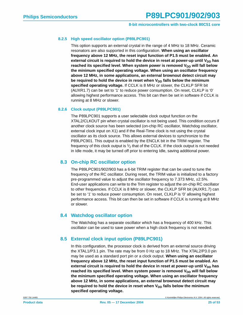
8.2.5 High speed oscillator option (P89LPC901)
This option supports an external crystal in the range of 4 MHz to 18 MHz. Ceramicresonators are also supported in this configuration. When using an oscillatorfrequency above 12 MHz, the reset input function of P1.5 must be enabled. Anexternal circuit is required to hold the device in reset at power-up until V DD hasreached its specified level. When system power is removed V DD will fall belowthe minimum specified operating voltage. When using an oscillator frequencyabove 12 MHz, in some applications, an external brownout detect circuit maybe required to hold the device in reset when V DD falls below the minimumspecified operating voltage. If CCLK is 8 MHz or slower, the CLKLP SFR bit(AUXR1.7) can be set to ‘1’ to reduce power consumption. On reset, CLKLP is ‘0’allowing highest performance access. This bit can then be set in software if CCLK isrunning at 8 MHz or slower.
8.2.6 Clock output (P89LPC901)
The P89LPC901 supports a user selectable clock output function on theXTAL2/CLKOUT pin when crystal oscillator is not being used. This condition occurs ifanother clock source has been selected (on-chip RC oscillator, Watchdog oscillator,external clock input on X1) and if the Real-Time clock is not using the crystaloscillator as its clock source. This allows external devices to synchronize to theP89LPC901. This output is enabled by the ENCLK bit in the TRIM register. Thefrequency of this clock output is 1⁄2 that of the CCLK. If the clock output is not neededin Idle mode, it may be turned off prior to entering Idle, saving additional power.
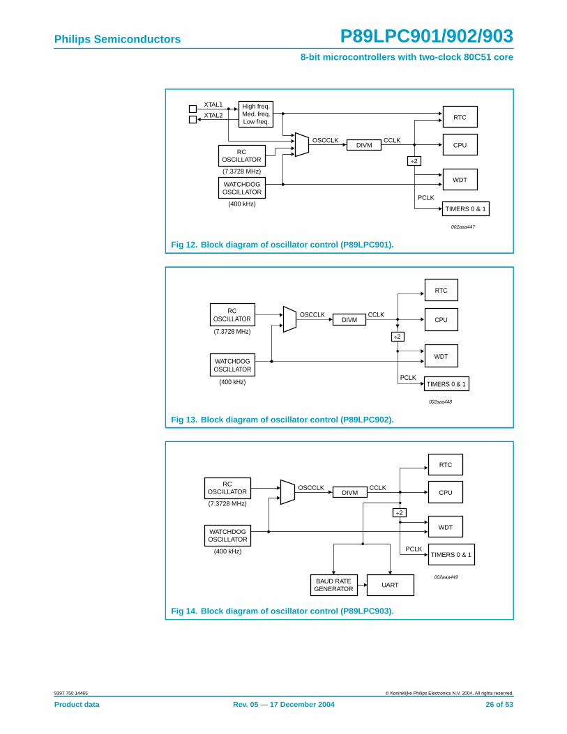
8.3 On-chip RC oscillator optionThe P89LPC901/902/903 has a 6-bit TRIM register that can be used to tune thefrequency of the RC oscillator. During reset, the TRIM value is initialized to a factorypre-programmed value to adjust the oscillator frequency to 7.373 MHz, ±2.5%.End-user applications can write to the Trim register to adjust the on-chip RC oscillatorto other frequencies. If CCLK is 8 MHz or slower, the CLKLP SFR bit (AUXR1.7) canbe set to ‘1’ to reduce power consumption. On reset, CLKLP is ‘0’ allowing highestperformance access. This bit can then be set in software if CCLK is running at 8 MHzor slower.
8.4 Watchdog oscillator optionThe Watchdog has a separate oscillator which has a frequency of 400 kHz. Thisoscillator can be used to save power when a high clock frequency is not needed.
8.5 External clock input option (P89LPC901)In this configuration, the processor clock is derived from an external source drivingthe XTAL1/P3.1 pin. The rate may be from 0 Hz up to 18 MHz. The XTAL2/P3.0 pinmay be used as a standard port pin or a clock output. When using an oscillatorfrequency above 12 MHz, the reset input function of P1.5 must be enabled. Anexternal circuit is required to hold the device in reset at power-up until V DD hasreached its specified level. When system power is removed V DD will fall belowthe minimum specified operating voltage. When using an oscillator frequencyabove 12 MHz, in some applications, an external brownout detect circuit maybe required to hold the device in reset when V DD falls below the minimumspecified operating voltage.
Product data Rev. 05 — 17 December 2004 25 of 53
9397 750 14465 © Koninklijke Philips Electronics N.V. 2004. All rights reserved.
Philips Semiconductors P89LPC901/902/9038-bit microcontrollers with two-clock 80C51 core
Fig 12. Block diagram of oscillator control (P89LPC901).
Fig 13. Block diagram of oscillator control (P89LPC902).
Fig 14. Block diagram of oscillator control (P89LPC903).
¸2
002aaa447
RTC
CPU
WDT
DIVMCCLKOSCCLK
PCLK
TIMERS 0 & 1
High freq.Med. freq.Low freq.
XTAL1
XTAL2
RCOSCILLATOR
WATCHDOGOSCILLATOR
(7.3728 MHz)
(400 kHz)
¸2
002aaa448
RTC
CPU
WDT
DIVMCCLKOSCCLK
PCLKTIMERS 0 & 1
RCOSCILLATOR
WATCHDOGOSCILLATOR
(7.3728 MHz)
(400 kHz)
¸2
002aaa449
RTC
CPU
WDT
DIVMCCLKOSCCLK
PCLKTIMERS 0 & 1
RCOSCILLATOR
WATCHDOGOSCILLATOR
(7.3728 MHz)
(400 kHz)
BAUD RATEGENERATOR
UART
Product data Rev. 05 — 17 December 2004 26 of 53
9397 750 14465 © Koninklijke Philips Electronics N.V. 2004. All rights reserved.
Philips Semiconductors P89LPC901/902/9038-bit microcontrollers with two-clock 80C51 core
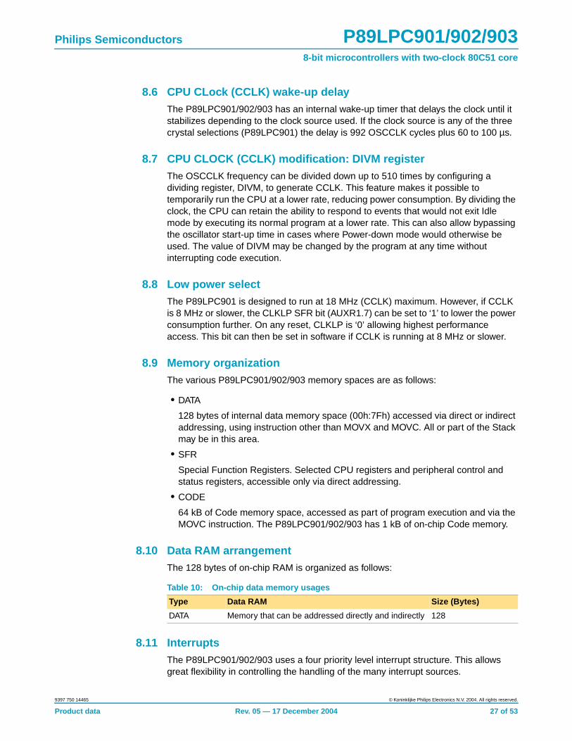
8.6 CPU CLock (CCLK) wake-up delayThe P89LPC901/902/903 has an internal wake-up timer that delays the clock until itstabilizes depending to the clock source used. If the clock source is any of the threecrystal selections (P89LPC901) the delay is 992 OSCCLK cycles plus 60 to 100 µs.
8.7 CPU CLOCK (CCLK) modification: DIVM registerThe OSCCLK frequency can be divided down up to 510 times by configuring adividing register, DIVM, to generate CCLK. This feature makes it possible totemporarily run the CPU at a lower rate, reducing power consumption. By dividing theclock, the CPU can retain the ability to respond to events that would not exit Idlemode by executing its normal program at a lower rate. This can also allow bypassingthe oscillator start-up time in cases where Power-down mode would otherwise beused. The value of DIVM may be changed by the program at any time withoutinterrupting code execution.
8.8 Low power selectThe P89LPC901 is designed to run at 18 MHz (CCLK) maximum. However, if CCLKis 8 MHz or slower, the CLKLP SFR bit (AUXR1.7) can be set to ‘1’ to lower the powerconsumption further. On any reset, CLKLP is ‘0’ allowing highest performanceaccess. This bit can then be set in software if CCLK is running at 8 MHz or slower.
8.9 Memory organizationThe various P89LPC901/902/903 memory spaces are as follows:
• DATA
128 bytes of internal data memory space (00h:7Fh) accessed via direct or indirectaddressing, using instruction other than MOVX and MOVC. All or part of the Stackmay be in this area.
• SFR
Special Function Registers. Selected CPU registers and peripheral control andstatus registers, accessible only via direct addressing.
• CODE
64 kB of Code memory space, accessed as part of program execution and via theMOVC instruction. The P89LPC901/902/903 has 1 kB of on-chip Code memory.
8.10 Data RAM arrangementThe 128 bytes of on-chip RAM is organized as follows:
8.11 InterruptsThe P89LPC901/902/903 uses a four priority level interrupt structure. This allowsgreat flexibility in controlling the handling of the many interrupt sources.
Table 10: On-chip data memory usages
Type Data RAM Size (Bytes)
DATA Memory that can be addressed directly and indirectly 128
Product data Rev. 05 — 17 December 2004 27 of 53
9397 750 14465 © Koninklijke Philips Electronics N.V. 2004. All rights reserved.

Philips Semiconductors P89LPC901/902/9038-bit microcontrollers with two-clock 80C51 core
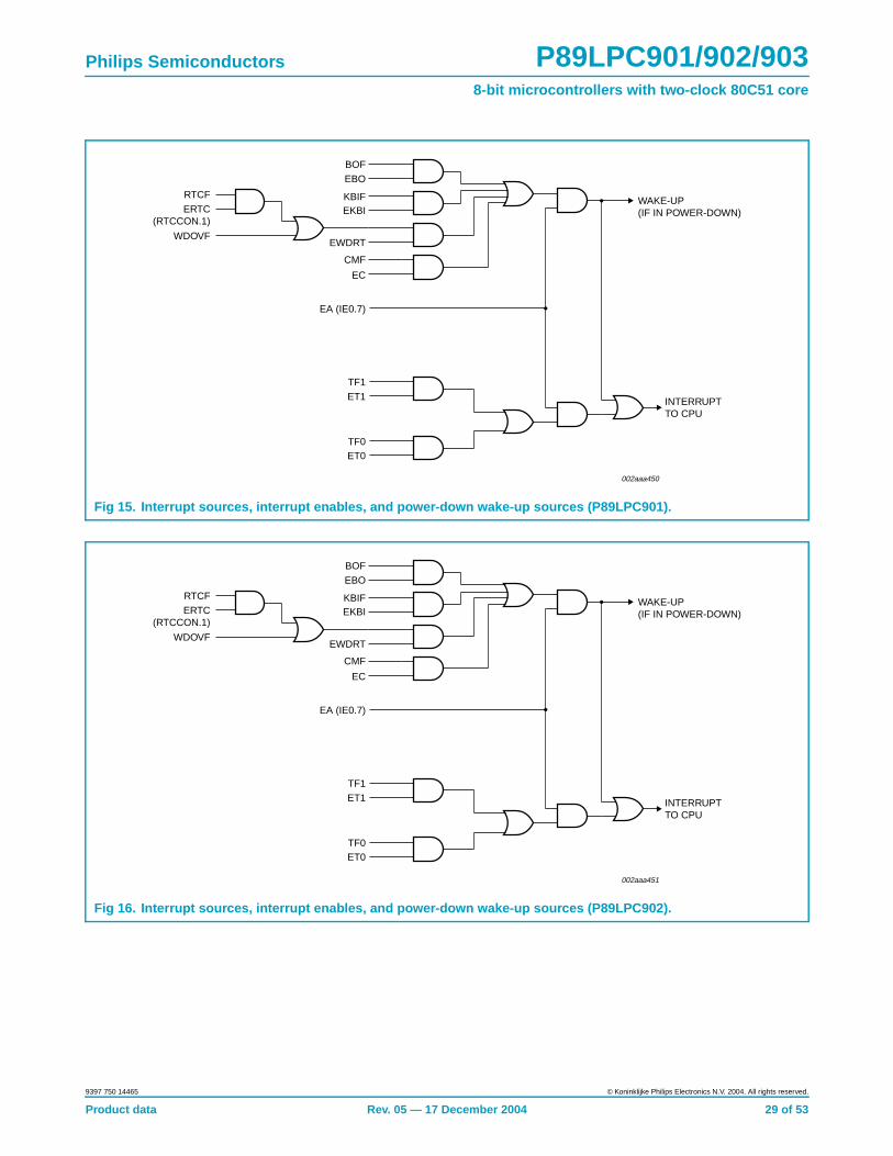
The P89LPC901 supports 6 interrupt sources: timers 0 and 1, brownout detect,Watchdog/real-time clock, keyboard, and the comparator.
The P89LPC902 supports 6 interrupt sources: timers 0 and 1, brownout detect,Watchdog/real-time clock, keyboard, and comparators 1 and 2.
The P89LPC903 supports 9 interrupt sources: timers 0 and 1, serial port Tx, serialport Rx, combined serial port Rx/Tx, brownout detect, Watchdog/real-time clock,keyboard, and comparators 1 and 2.
Each interrupt source can be individually enabled or disabled by setting or clearing abit in the interrupt enable registers IEN0 or IEN1. The IEN0 register also contains aglobal disable bit, EA, which disables all interrupts.
Each interrupt source can be individually programmed to one of four priority levels bysetting or clearing bits in the interrupt priority registers IP0, IP0H, IP1, and IP1H. Aninterrupt service routine in progress can be interrupted by a higher priority interrupt,but not by another interrupt of the same or lower priority. The highest priority interruptservice cannot be interrupted by any other interrupt source. If two requests ofdifferent priority levels are pending at the start of an instruction, the request of higherpriority level is serviced.
If requests of the same priority level are pending at the start of an instruction, aninternal polling sequence determines which request is serviced. This is called thearbitration ranking. Note that the arbitration ranking is only used to resolve pendingrequests of the same priority level.
8.11.1 External interrupt inputs
The P89LPC901/902/903 has a Keypad Interrupt function. This can be used as anexternal interrupt input.
If enabled when the P89LPC901/902/903 is put into Power-down or Idle mode, theinterrupt will cause the processor to wake-up and resume operation. Refer to Section8.14 “Power reduction modes” for details.
Product data Rev. 05 — 17 December 2004 28 of 53
9397 750 14465 © Koninklijke Philips Electronics N.V. 2004. All rights reserved.
Philips Semiconductors P89LPC901/902/9038-bit microcontrollers with two-clock 80C51 core
Fig 15. Interrupt sources, interrupt enables, and power-down wake-up sources (P89LPC901).
002aaa450
BOFEBO
KBIFEKBI
INTERRUPT TO CPU
WAKE-UP(IF IN POWER-DOWN)
EWDRT
CMF
EC
EA (IE0.7)
TF1ET1
TF0ET0
RTCFERTC
(RTCCON.1)
WDOVF
Fig 16. Interrupt sources, interrupt enables, and power-down wake-up sources (P89LPC902).
002aaa451
BOFEBO
KBIFEKBI
INTERRUPT TO CPU
WAKE-UP(IF IN POWER-DOWN)
EWDRT
CMF
EC
EA (IE0.7)
TF1ET1
TF0ET0
RTCFERTC
(RTCCON.1)
WDOVF
Product data Rev. 05 — 17 December 2004 29 of 53
9397 750 14465 © Koninklijke Philips Electronics N.V. 2004. All rights reserved.

Philips Semiconductors P89LPC901/902/9038-bit microcontrollers with two-clock 80C51 core
8.12 I/O portsThe P89LPC901 has between 3 and 6 I/O pins: P0.4, P0.5, P1.2, P1.5, P3.0, andP3.1 The exact number of I/O pins available depends on the clock and reset optionschosen, as shown in Table 11.
[1] Required for operation above 12 MHz.
The P89LPC902 and P89LPC903 devices have either 5 or 6 I/O pins depending onthe reset pin option chosen.
8.12.1 Port configurations
All but one I/O port pin on the P89LPC901/902/903 may be configured by software toone of four types on a bit-by-bit basis. These are: quasi-bidirectional (standard 80C51port outputs), push-pull, open drain, and input-only. Two configuration registers foreach port select the output type for each port pin.
P1.5 (RST) can only be an input and cannot be configured.
Fig 17. Interrupt sources, interrupt enables, and power-down wake-up sources (P89LPC903).
002aaa452
BOFEBO
KBIFEKBI
INTERRUPT TO CPU
WAKE-UP(IF IN POWER-DOWN)
EWDRT
CMF
EC
EA (IE0.7)
RTCFERTC
(RTCCON.1)
WDOVF
TF1ET1
TI & RI/RIES/ESR
TIEST
TF0ET0
Table 11: Number of I/O pins available
Clock source Reset option Number of I/O pins(8-pin package)
On-chip oscillator or Watchdog oscillator No external reset (except during power-up) 6
External RST pin supported 5
External clock input No external reset (except during power-up) 5
External RST pin supported[1] 4
Low/medium/high speed oscillator(external crystal or resonator)
No external reset (except during power-up) 4
External RST pin supported[1] 3
Product data Rev. 05 — 17 December 2004 30 of 53
9397 750 14465 © Koninklijke Philips Electronics N.V. 2004. All rights reserved.
Philips Semiconductors P89LPC901/902/9038-bit microcontrollers with two-clock 80C51 core
8.12.2 Quasi-bidirectional output configuration
Quasi-bidirectional output type can be used as both an input and output without theneed to reconfigure the port. This is possible because when the port outputs a logicHIGH, it is weakly driven, allowing an external device to pull the pin LOW. When thepin is driven LOW, it is driven strongly and able to sink a fairly large current. Thesefeatures are somewhat similar to an open-drain output except that there are threepull-up transistors in the quasi-bidirectional output that serve different purposes.
The P89LPC901/902/903 is a 3 V device, however, the pins are 5 V-tolerant (exceptfor XTAL1 and XTAL2). In quasi-bidirectional mode, if a user applies 5 V on the pin,there will be a current flowing from the pin to VDD, causing extra power consumption.Therefore, applying 5 V in quasi-bidirectional mode is discouraged.
A quasi-bidirectional port pin has a Schmitt-triggered input that also has a glitchsuppression circuit.
8.12.3 Open-drain output configuration
The open-drain output configuration turns off all pull-ups and only drives thepull-down transistor of the port driver when the port latch contains a logic ‘0’. To beused as a logic output, a port configured in this manner must have an externalpull-up, typically a resistor tied to VDD.
An open-drain port pin has a Schmitt-triggered input that also has a glitchsuppression circuit.
8.12.4 Input-only configuration
The input-only port configuration has no output drivers. It is a Schmitt-triggered inputthat also has a glitch suppression circuit.
8.12.5 Push-pull output configuration
The push-pull output configuration has the same pull-down structure as both theopen-drain and the quasi-bidirectional output modes, but provides a continuousstrong pull-up when the port latch contains a logic ‘1’. The push-pull mode may beused when more source current is needed from a port output. A push-pull port pinhas a Schmitt-triggered input that also has a glitch suppression circuit.
8.12.6 Port 0 analog functions
The P89LPC901/902/903 incorporates an Analog Comparator. In order to give thebest analog function performance and to minimize power consumption, pins that arebeing used for analog functions must have the digital outputs and digital inputsdisabled.
Digital outputs are disabled by putting the port output into the Input-Only (highimpedance) mode as described in Section 8.12.4 “Input-only configuration”.
Digital inputs on Port 0 may be disabled through the use of the PT0AD register. Onany reset, the PT0AD bits default to ‘0’s to enable digital functions.
Product data Rev. 05 — 17 December 2004 31 of 53
9397 750 14465 © Koninklijke Philips Electronics N.V. 2004. All rights reserved.
Philips Semiconductors P89LPC901/902/9038-bit microcontrollers with two-clock 80C51 core
8.12.7 Additional port features
After power-up, all pins are in Input-Only mode. Please note that this is differentfrom the LPC76x series of devices.
• After power-up all I/O pins, except P1.5, may be configured by software.
• Pin P1.5 is input only.
Every output on the P89LPC901/902/903 has been designed to sink typical LEDdrive current. However, there is a maximum total output current for all ports whichmust not be exceeded. Please refer to Table 13 “DC electrical characteristics” fordetailed specifications.
All ports pins that can function as an output have slew rate controlled outputs to limitnoise generated by quickly switching output signals. The slew rate is factory-set toapproximately 10 ns rise and fall times.
8.13 Power monitoring functionsThe P89LPC901/902/903 incorporates power monitoring functions designed toprevent incorrect operation during initial power-up and power loss or reduction duringoperation. This is accomplished with two hardware functions: Power-on Detect andBrownout detect.
8.13.1 Brownout detection
The Brownout detect function determines if the power supply voltage drops below acertain level. The default operation is for a Brownout detection to cause a processorreset, however, it may alternatively be configured to generate an interrupt.
Brownout detection may be enabled or disabled in software.
If Brownout detection is enabled, the operating voltage range for VDD is 2.7 V to 3.6 V,and the brownout condition occurs when VDD falls below the brownout trip voltage,VBO (see Table 13 “DC electrical characteristics”), and is negated when VDD risesabove VBO. If brownout detection is disabled, the operating voltage range for VDD is2.4 V to 3.6 V. If the P89LPC901/902/903 device is to operate with a power supplythat can be below 2.7 V, BOE should be left in the unprogrammed state so that thedevice can operate at 2.4 V, otherwise continuous brownout reset may prevent thedevice from operating.
For correct activation of Brownout detect, the VDD rise and fall times must beobserved. Please see Table 13 “DC electrical characteristics” for specifications.
8.13.2 Power-on detection
The Power-on Detect has a function similar to the Brownout detect, but is designed towork as power comes up initially, before the power supply voltage reaches a levelwhere Brownout detect can work. The POF flag in the RSTSRC register is set toindicate an initial power-up condition. The POF flag will remain set until cleared bysoftware.
8.14 Power reduction modesThe P89LPC901/902/903 supports three different power reduction modes. Thesemodes are Idle mode, Power-down mode, and total Power-down mode.
Product data Rev. 05 — 17 December 2004 32 of 53
9397 750 14465 © Koninklijke Philips Electronics N.V. 2004. All rights reserved.
Philips Semiconductors P89LPC901/902/9038-bit microcontrollers with two-clock 80C51 core
8.14.1 Idle mode
Idle mode leaves peripherals running in order to allow them to activate the processorwhen an interrupt is generated. Any enabled interrupt source or reset may terminateIdle mode.
8.14.2 Power-down mode
The Power-down mode stops the oscillator in order to minimize power consumption.The P89LPC901/902/903 exits Power-down mode via any reset, or certain interrupts.In Power-down mode, the power supply voltage may be reduced to the RAMkeep-alive voltage VRAM. This retains the RAM contents at the point wherePower-down mode was entered. SFR contents are not guaranteed after VDD hasbeen lowered to VRAM, therefore it is highly recommended to wake up the processorvia reset in this case. VDD must be raised to within the operating range before thePower-down mode is exited.
Some chip functions continue to operate and draw power during Power-down mode,increasing the total power used during Power-down. These include: Brownout detect,Watchdog Timer, Comparators (note that Comparators can be powered-downseparately), and Real-Time Clock (RTC)/System Timer. The internal RC oscillator isdisabled unless both the RC oscillator has been selected as the system clock and theRTC is enabled.
8.14.3 Total Power-down mode
This is the same as Power-down mode except that the brownout detection circuitryand the voltage comparators are also disabled to conserve additional power. Theinternal RC oscillator is disabled unless both the RC oscillator has been selected asthe system clock and the RTC is enabled. If the internal RC oscillator is used to clockthe RTC during Power-down, there will be high power consumption. Please use anexternal low frequency clock to achieve low power with the Real-Time Clock runningduring Power-down.
8.15 ResetThe P1.5/RST pin can function as either an active-LOW reset input or as a digitalinput, P1.5. The RPE (Reset Pin Enable) bit in UCFG1, when set to ‘1’, enables theexternal reset input function on P1.5. When cleared, P1.5 may be used as an inputpin.
Remark: During a power-up sequence, the RPE selection is overridden and this pinwill always function as a reset input. An external circuit connected to this pinshould not hold this pin LOW during a power-on sequence as this will keep thedevice in reset. After power-up this input will function either as an external resetinput or as a digital input as defined by the RPE bit. Only a power-up reset willtemporarily override the selection defined by RPE bit. Other sources of reset will notoverride the RPE bit.
Remark: During a power cycle, VDD must fall below VPOR (see Table 13 “DC electricalcharacteristics”) before power is reapplied, in order to ensure a power-on reset.
Product data Rev. 05 — 17 December 2004 33 of 53
9397 750 14465 © Koninklijke Philips Electronics N.V. 2004. All rights reserved.

Philips Semiconductors P89LPC901/902/9038-bit microcontrollers with two-clock 80C51 core
Reset can be triggered from the following sources:
• External reset pin (during power-up or if user configured via UCFG1. This optionmust be used for an oscillator frequency above 12 MHz.)
• Power-on detect
• Brownout detect
• Watchdog Timer
• Software reset
• UART break character detect reset (P80LPC903).
For every reset source, there is a flag in the Reset Register, RSTSRC. The user canread this register to determine the most recent reset source. These flag bits can becleared in software by writing a ‘0’ to the corresponding bit. More than one flag bitmay be set:
• During a power-on reset, both POF and BOF are set but the other flag bits arecleared.
• For any other reset, previously set flag bits that have not been cleared will remainset.
8.16 Timers/counters 0 and 1The P89LPC901/902/903 has two general purpose timers which are similar to thestandard 80C51 Timer 0 and Timer 1. These timers have four operating modes(modes 0, 1, 2, and 3). Modes 0, 1, and 2 are the same for both Timers. Mode 3 isdifferent.
8.16.1 Mode 0
Putting either Timer into Mode 0 makes it look like an 8048 Timer, which is an 8-bitCounter with a divide-by-32 prescaler. In this mode, the Timer register is configuredas a 13-bit register. Mode 0 operation is the same for Timer 0 and Timer 1.
8.16.2 Mode 1
Mode 1 is the same as Mode 0, except that all 16 bits of the timer register are used.
8.16.3 Mode 2
Mode 2 configures the Timer register as an 8-bit Counter with automatic reload.Mode 2 operation is the same for Timer 0 and Timer 1.
8.16.4 Mode 3
When Timer 1 is in Mode 3 it is stopped. Timer 0 in Mode 3 forms two separate 8-bitcounters and is provided for applications that require an extra 8-bit timer. WhenTimer 1 is in Mode 3 it can still be used by the serial port as a baud rate generator.
8.16.5 Mode 6 (P89LPC901)
In this mode, the corresponding timer can be changed to a PWM with a full period of256 timer clocks.
Product data Rev. 05 — 17 December 2004 34 of 53
9397 750 14465 © Koninklijke Philips Electronics N.V. 2004. All rights reserved.

Philips Semiconductors P89LPC901/902/9038-bit microcontrollers with two-clock 80C51 core
8.16.6 Timer overflow toggle output (P89LPC901)
Timers 0 and 1 can be configured to automatically toggle a port output whenever atimer overflow occurs. The same device pins that are used for the T0 and T1 countinputs are also used for the timer toggle outputs. The port outputs will be a logic 1prior to the first timer overflow when this mode is turned on.
8.17 Real-Time clock/system timerThe P89LPC901/902/903 has a simple Real-Time clock that allows a user to continuerunning an accurate timer while the rest of the device is powered-down. TheReal-Time clock can be a wake-up or an interrupt source. The Real-Time clock is a23-bit down counter comprised of a 7-bit prescaler and a 16-bit loadable downcounter. When it reaches all ‘0’s, the counter will be reloaded again and the RTCFflag will be set. The clock source for this counter can be either the CPU clock (CCLK)or the XTAL oscillator, provided that the XTAL oscillator is not being used as the CPUclock. If the XTAL oscillator is used as the CPU clock, then the RTC will use CCLK asits clock source. Only power-on reset will reset the Real-Time clock and itsassociated SFRs to the default state.
8.18 UART (P89LPC903)The P89LPC903 has an enhanced UART that is compatible with the conventional80C51 UART except that Timer 2 overflow cannot be used as a baud rate source.The P89LPC903 does include an independent Baud Rate Generator. The baud ratecan be selected from the oscillator (divided by a constant), Timer 1 overflow, or theindependent Baud Rate Generator. In addition to the baud rate generation,enhancements over the standard 80C51 UART include Framing Error detection,automatic address recognition, selectable double buffering and several interruptoptions. The UART can be operated in 4 modes: shift register, 8-bit UART, 9-bitUART, and CPU clock/32 or CPU clock/16.
8.18.1 Mode 0
Serial data enters and exits through RxD. TxD outputs the shift clock. 8 bits aretransmitted or received, LSB first. The baud rate is fixed at 1⁄16 of the CPU clockfrequency.
8.18.2 Mode 1
10 bits are transmitted (through TxD) or received (through RxD): a start bit(logical ‘0’), 8 data bits (LSB first), and a stop bit (logical ‘1’). When data is received,the stop bit is stored in RB8 in Special Function Register SCON. The baud rate isvariable and is determined by the Timer 1 overflow rate or the Baud Rate Generator(described in Section 8.18.5 “Baud rate generator and selection”).
8.18.3 Mode 2
11 bits are transmitted (through TxD) or received (through RxD): start bit (logical ‘0’),8 data bits (LSB first), a programmable 9th data bit, and a stop bit (logical ‘1’). Whendata is transmitted, the 9th data bit (TB8 in SCON) can be assigned the value of ‘0’ or‘1’. Or, for example, the parity bit (P, in the PSW) could be moved into TB8. Whendata is received, the 9th data bit goes into RB8 in Special Function Register SCON,while the stop bit is not saved. The baud rate is programmable to either 1⁄16 or 1⁄32 ofthe CPU clock frequency, as determined by the SMOD1 bit in PCON.
Product data Rev. 05 — 17 December 2004 35 of 53
9397 750 14465 © Koninklijke Philips Electronics N.V. 2004. All rights reserved.
Philips Semiconductors P89LPC901/902/9038-bit microcontrollers with two-clock 80C51 core
8.18.4 Mode 3
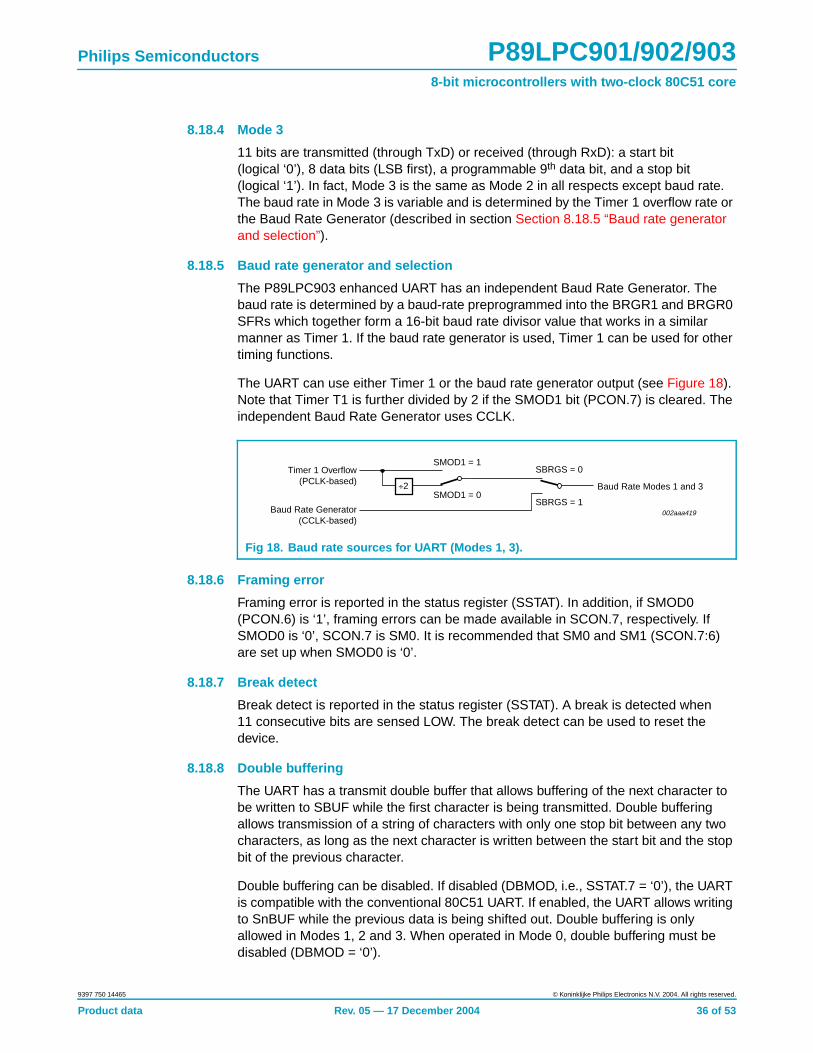
11 bits are transmitted (through TxD) or received (through RxD): a start bit(logical ‘0’), 8 data bits (LSB first), a programmable 9th data bit, and a stop bit(logical ‘1’). In fact, Mode 3 is the same as Mode 2 in all respects except baud rate.The baud rate in Mode 3 is variable and is determined by the Timer 1 overflow rate orthe Baud Rate Generator (described in section Section 8.18.5 “Baud rate generatorand selection”).
8.18.5 Baud rate generator and selection
The P89LPC903 enhanced UART has an independent Baud Rate Generator. Thebaud rate is determined by a baud-rate preprogrammed into the BRGR1 and BRGR0SFRs which together form a 16-bit baud rate divisor value that works in a similarmanner as Timer 1. If the baud rate generator is used, Timer 1 can be used for othertiming functions.
The UART can use either Timer 1 or the baud rate generator output (see Figure 18).Note that Timer T1 is further divided by 2 if the SMOD1 bit (PCON.7) is cleared. Theindependent Baud Rate Generator uses CCLK.
8.18.6 Framing error
Framing error is reported in the status register (SSTAT). In addition, if SMOD0(PCON.6) is ‘1’, framing errors can be made available in SCON.7, respectively. IfSMOD0 is ‘0’, SCON.7 is SM0. It is recommended that SM0 and SM1 (SCON.7:6)are set up when SMOD0 is ‘0’.
8.18.7 Break detect
Break detect is reported in the status register (SSTAT). A break is detected when11 consecutive bits are sensed LOW. The break detect can be used to reset thedevice.
8.18.8 Double buffering
The UART has a transmit double buffer that allows buffering of the next character tobe written to SBUF while the first character is being transmitted. Double bufferingallows transmission of a string of characters with only one stop bit between any twocharacters, as long as the next character is written between the start bit and the stopbit of the previous character.
Double buffering can be disabled. If disabled (DBMOD, i.e., SSTAT.7 = ‘0’), the UARTis compatible with the conventional 80C51 UART. If enabled, the UART allows writingto SnBUF while the previous data is being shifted out. Double buffering is onlyallowed in Modes 1, 2 and 3. When operated in Mode 0, double buffering must bedisabled (DBMOD = ‘0’).
Fig 18. Baud rate sources for UART (Modes 1, 3).
Baud Rate Modes 1 and 3
SBRGS = 1
SBRGS = 0
SMOD1 = 0
SMOD1 = 1
¸2
Timer 1 Overflow(PCLK-based)
Baud Rate Generator(CCLK-based)
002aaa419
Product data Rev. 05 — 17 December 2004 36 of 53
9397 750 14465 © Koninklijke Philips Electronics N.V. 2004. All rights reserved.

Philips Semiconductors P89LPC901/902/9038-bit microcontrollers with two-clock 80C51 core
8.18.9 Transmit interrupts with double buffering enabled (Modes 1, 2 and 3)
Unlike the conventional UART, in double buffering mode, the Tx interrupt is generatedwhen the double buffer is ready to receive new data.
8.18.10 The 9th bit (bit 8) in double buffering (Modes 1, 2 and 3)
If double buffering is disabled TB8 can be written before or after SBUF is written, aslong as TB8 is updated some time before that bit is shifted out. TB8 must not bechanged until the bit is shifted out, as indicated by the Tx interrupt.
If double buffering is enabled, TB8 must be updated before SBUF is written, as TB8will be double-buffered together with SBUF data.
8.19 Analog comparatorsOne analog comparator is provided on the P89LPC901. Two analog comparators areprovided on the P89LPC902 and P89LPC903 devices. Comparator operation is suchthat the output is a logical one (which may be read in a register) when the positiveinput is greater than the negative input (selectable from a pin or an internal referencevoltage). Otherwise the output is a zero. The comparator may be configured to causean interrupt when the output value changes.
The connections to the comparator are shown in Figure 19. Note: Not all possiblecomparator configurations are available on all three devices. Please refer to the Logicdiagrams in Section 6 “Logic symbols” on page 12. The comparator functions toVDD = 2.4 V.
When the comparator is first enabled, the comparator output and interrupt flag are notguaranteed to be stable for 10 microseconds. The comparator interrupt should not beenabled during that time, and the comparator interrupt flag must be cleared beforethe interrupt is enabled in order to prevent an immediate interrupt service.
When a comparator is disabled the comparator’s output, COx, goes HIGH. If thecomparator output was LOW and then is disabled, the resulting transition of thecomparator output from a LOW to HIGH state will set the comparator flag, CMFx.This will cause an interrupt if the comparator interrupt is enabled. The user shouldtherefore disable the comparator interrupt prior to disabling the comparator.Additionally, the user should clear the comparator flag, CMFx, after disabling thecomparator.
Product data Rev. 05 — 17 December 2004 37 of 53
9397 750 14465 © Koninklijke Philips Electronics N.V. 2004. All rights reserved.
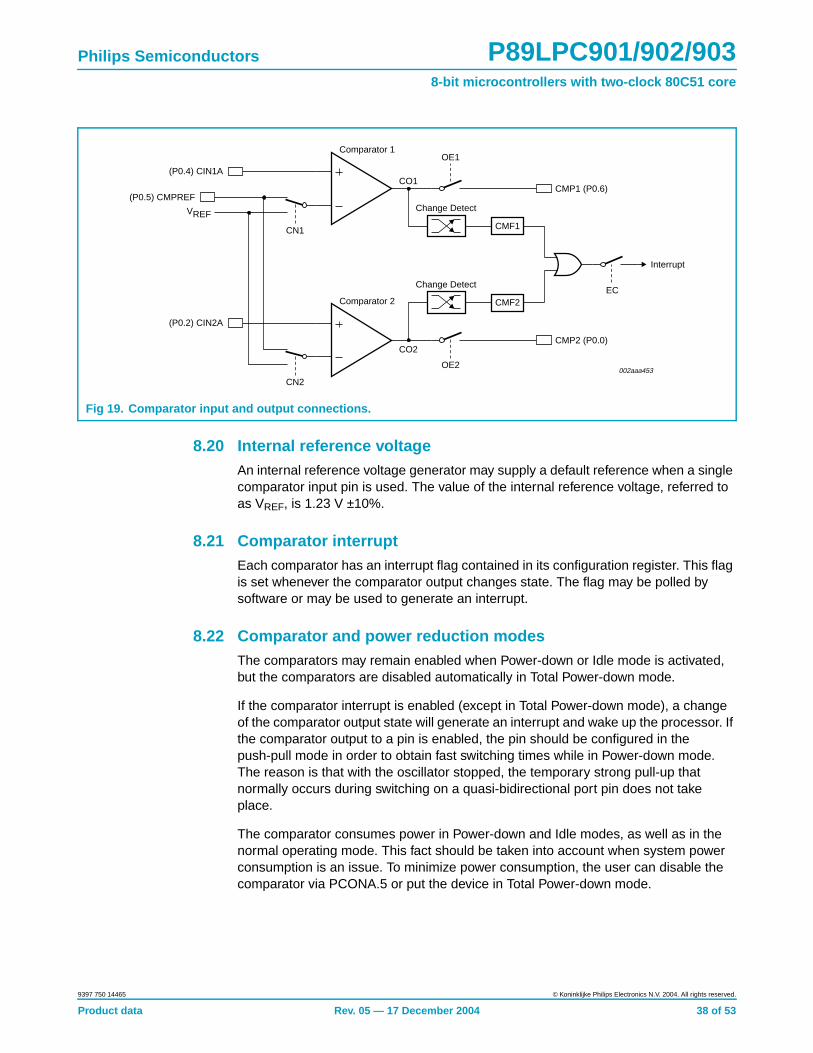
Philips Semiconductors P89LPC901/902/9038-bit microcontrollers with two-clock 80C51 core
8.20 Internal reference voltageAn internal reference voltage generator may supply a default reference when a singlecomparator input pin is used. The value of the internal reference voltage, referred toas VREF, is 1.23 V ±10%.
8.21 Comparator interruptEach comparator has an interrupt flag contained in its configuration register. This flagis set whenever the comparator output changes state. The flag may be polled bysoftware or may be used to generate an interrupt.
8.22 Comparator and power reduction modesThe comparators may remain enabled when Power-down or Idle mode is activated,but the comparators are disabled automatically in Total Power-down mode.
If the comparator interrupt is enabled (except in Total Power-down mode), a changeof the comparator output state will generate an interrupt and wake up the processor. Ifthe comparator output to a pin is enabled, the pin should be configured in thepush-pull mode in order to obtain fast switching times while in Power-down mode.The reason is that with the oscillator stopped, the temporary strong pull-up thatnormally occurs during switching on a quasi-bidirectional port pin does not takeplace.
The comparator consumes power in Power-down and Idle modes, as well as in thenormal operating mode. This fact should be taken into account when system powerconsumption is an issue. To minimize power consumption, the user can disable thecomparator via PCONA.5 or put the device in Total Power-down mode.
Fig 19. Comparator input and output connections.
Comparator 1
CN1
(P0.4) CIN1A
(P0.5) CMPREF
VREF
OE1
Change Detect
CO1
CMF1
Interrupt
002aaa453
CMP1 (P0.6)
ECChange Detect
CMF2Comparator 2
OE2
CO2CMP2 (P0.0)
CN2
(P0.2) CIN2A
Product data Rev. 05 — 17 December 2004 38 of 53
9397 750 14465 © Koninklijke Philips Electronics N.V. 2004. All rights reserved.

Philips Semiconductors P89LPC901/902/9038-bit microcontrollers with two-clock 80C51 core
8.23 Keypad interrupt (KBI)The Keypad Interrupt function is intended primarily to allow a single interrupt to begenerated when Port 0 is equal to or not equal to a certain pattern. This function canbe used for bus address recognition or keypad recognition. The user can configurethe port via SFRs for different tasks.
The Keypad Interrupt Mask Register (KBMASK) is used to define which input pinsconnected to Port 0 can trigger the interrupt. The Keypad Pattern Register (KBPATN)is used to define a pattern that is compared to the value of Port 0. The KeypadInterrupt Flag (KBIF) in the Keypad Interrupt Control Register (KBCON) is set whenthe condition is matched while the Keypad Interrupt function is active. An interrupt willbe generated if enabled. The PATN_SEL bit in the Keypad Interrupt Control Register(KBCON) is used to define equal or not-equal for the comparison.
In order to use the Keypad Interrupt as an original KBI function like in 87LPC76xseries, the user needs to set KBPATN = 0FFH and PATN_SEL = 1 (not equal), thenany key connected to Port 0 which is enabled by the KBMASK register will cause thehardware to set KBIF and generate an interrupt if it has been enabled. The interruptmay be used to wake up the CPU from Idle or Power-down modes. This feature isparticularly useful in handheld, battery powered systems that need to carefullymanage power consumption yet also need to be convenient to use.
In order to set the flag and cause an interrupt, the pattern on Port 0 must be heldlonger than six CCLKs.
8.24 Watchdog timerThe Watchdog timer causes a system reset when it underflows as a result of a failureto feed the timer prior to the timer reaching its terminal count. It consists of aprogrammable 12-bit prescaler, and an 8-bit down counter. The down counter isdecremented by a tap taken from the prescaler. The clock source for the prescaler iseither the PCLK or the nominal 400 kHz Watchdog oscillator. The Watchdog timercan only be reset by a power-on reset. When the Watchdog feature is disabled, it canbe used as an interval timer and may generate an interrupt. Figure 20 shows theWatchdog timer in Watchdog mode. Feeding the watchdog requires a two-bytesequence. If PCLK is selected as the Watchdog clock and the CPU is powered-down,the watchdog is disabled. The Watchdog timer has a time-out period that ranges froma few µs to a few seconds. Please refer to the P89LPC901/902/903 User’s Manual formore details.
Product data Rev. 05 — 17 December 2004 39 of 53
9397 750 14465 © Koninklijke Philips Electronics N.V. 2004. All rights reserved.
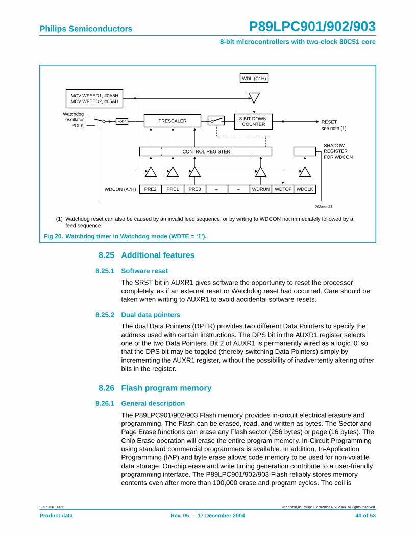
Philips Semiconductors P89LPC901/902/9038-bit microcontrollers with two-clock 80C51 core
8.25 Additional features
8.25.1 Software reset
The SRST bit in AUXR1 gives software the opportunity to reset the processorcompletely, as if an external reset or Watchdog reset had occurred. Care should betaken when writing to AUXR1 to avoid accidental software resets.
8.25.2 Dual data pointers
The dual Data Pointers (DPTR) provides two different Data Pointers to specify theaddress used with certain instructions. The DPS bit in the AUXR1 register selectsone of the two Data Pointers. Bit 2 of AUXR1 is permanently wired as a logic ‘0’ sothat the DPS bit may be toggled (thereby switching Data Pointers) simply byincrementing the AUXR1 register, without the possibility of inadvertently altering otherbits in the register.
8.26 Flash program memory
8.26.1 General description
The P89LPC901/902/903 Flash memory provides in-circuit electrical erasure andprogramming. The Flash can be erased, read, and written as bytes. The Sector andPage Erase functions can erase any Flash sector (256 bytes) or page (16 bytes). TheChip Erase operation will erase the entire program memory. In-Circuit Programmingusing standard commercial programmers is available. In addition, In-ApplicationProgramming (IAP) and byte erase allows code memory to be used for non-volatiledata storage. On-chip erase and write timing generation contribute to a user-friendlyprogramming interface. The P89LPC901/902/903 Flash reliably stores memorycontents even after more than 100,000 erase and program cycles. The cell is
(1) Watchdog reset can also be caused by an invalid feed sequence, or by writing to WDCON not immediately followed by afeed sequence.
Fig 20. Watchdog timer in Watchdog mode (WDTE = ‘1’).
PRE2 PRE1 PRE0 – – WDRUN WDTOF WDCLKWDCON (A7H)
CONTROL REGISTER
PRESCALER
002aaa423
SHADOW REGISTERFOR WDCON
8-BIT DOWN COUNTER
WDL (C1H)
Watchdogoscillator
PCLK÷32
MOV WFEED1, #0A5HMOV WFEED2, #05AH
RESETsee note (1)
Product data Rev. 05 — 17 December 2004 40 of 53
9397 750 14465 © Koninklijke Philips Electronics N.V. 2004. All rights reserved.
Philips Semiconductors P89LPC901/902/9038-bit microcontrollers with two-clock 80C51 core
designed to optimize the erase and programming mechanisms. TheP89LPC901/902/903 uses VDD as the supply voltage to perform the Program/Erasealgorithms.
8.26.2 Features
• Programming and erase over the full operating voltage range.
• Byte-erase allowing code memory to be used for data storage.
• Read/Programming/Erase using ICP.
• Any flash program/erase operation in 2 ms.
• Programming with industry-standard commercial programmers.
• Programmable security for the code in the Flash for each sector.
• More than 100,000 minimum erase/program cycles for each byte.
• 10-year minimum data retention.
8.26.3 Flash organization
The P89LPC901/902/903 program memory consists of four 256 byte sectors. Eachsector can be further divided into 16-byte pages. In addition to sector erase, pageerase, and byte erase, a 16-byte page register is included which allows from 1 to 16bytes of a given page to be programmed at the same time, substantially reducingoverall programming time. In addition, erasing and reprogramming ofuser-programmable configuration bytes including UCFG1, the Boot Status Bit, andthe Boot Vector is supported.
8.26.4 Flash programming and erasing
Different methods of erasing or programming of the Flash are available. The Flashmay be programmed or erased in the end-user application (IAP) under control of theapplication’s firmware. Another option is to use the In-Circuit Programming (ICP)mechanism. This ICP system provides for programming through a serial clock- serialdata interface. Third, the Flash may be programmed or erased using a commerciallyavailable EPROM programmer which supports this device. This device does notprovide for direct verification of code memory contents. Instead this device provides a32-bit CRC result on either a sector or the entire 1 KB of user code space.
8.26.5 In-circuit programming (ICP)
In-Circuit Programming is performed without removing the microcontroller from thesystem. The In-Circuit Programming facility consists of internal hardware resourcesto facilitate remote programming of the P89LPC901/902/903 through a two-wireserial interface. The Philips In-Circuit Programming facility has made in-circuitprogramming in an embedded application, using commercially availableprogrammers, possible with a minimum of additional expense in components andcircuit board area. The ICP function uses five pins. Only a small connector needs tobe available to interface your application to a commercial programmer in order to usethis feature. Additional details may be found in the P89LPC901/902/903 User’sManual.
Product data Rev. 05 — 17 December 2004 41 of 53
9397 750 14465 © Koninklijke Philips Electronics N.V. 2004. All rights reserved.

Philips Semiconductors P89LPC901/902/9038-bit microcontrollers with two-clock 80C51 core
8.26.6 In-application programming
In-Application Programming is performed in the application under the control of themicrocontroller’s firmware. The IAP facility consists of internal hardware resources tofacilitate programming and erasing. The Philips In-Application Programming hasmade in-application programming in an embedded application possible withoutadditional components. This is accomplished through the use of four SFRs consistingof a control/status register, a data register, and two address registers. Additionaldetails may be found in the P89LPC901/902/903 User’s Manual.
8.26.7 Using flash as data storage
The Flash code memory array of this device supports individual byte erasing andprogramming. Any byte in the code memory array may be read using the MOVCinstruction, provided that the sector containing the byte has not been secured (aMOVC instruction is not allowed to read code memory contents of a secured sector).Thus any byte in a non-secured sector may be used for non-volatile data storage.
8.26.8 User configuration bytes
Some user-configurable features of the P89LPC901/902/903 must be defined atpower-up and therefore cannot be set by the program after start of execution. Thesefeatures are configured through the use of the Flash byte UCFG1. Please see theP89LPC901/902/903 User’s Manual for additional details.
8.26.9 User sector security bytes
There are four User Sector Security Bytes, each corresponding to one sector. Pleasesee the P89LPC901/902/903 User’s Manual for additional details.
Product data Rev. 05 — 17 December 2004 42 of 53
9397 750 14465 © Koninklijke Philips Electronics N.V. 2004. All rights reserved.

Philips Semiconductors P89LPC901/902/9038-bit microcontrollers with two-clock 80C51 core
9. Limiting values
[1] The following applies to Limiting values:
a) Stresses above those listed under Table 12 may cause permanent damage to the device. This is a stress rating only and functionaloperation of the device at these or any conditions other than those described in Table 13 “DC electrical characteristics”, Table 14 “ACcharacteristics” and Table 15 “AC characteristics (P89LPC901)” of this specification are not implied.
b) This product includes circuitry specifically designed for the protection of its internal devices from the damaging effects of excessivestatic charge. Nonetheless, it is suggested that conventional precautions be taken to avoid applying greater than the rated maximum.
c) Parameters are valid over operating temperature range unless otherwise specified. All voltages are with respect to VSS unlessotherwise noted.
Table 12: Limiting valuesIn accordance with the Absolute Maximum Rating System (IEC 60134).[1]
Symbol Parameter Conditions Min Max Unit
Tamb(bias) operating bias ambient temperature −55 +125 °C
Tstg storage temperature range −65 +150 °C
Vxtal voltage on XTAL1, XTAL2 pin to VSS,as applicable
- VDD + 0.5 V
Vn voltage on any other pin to VSS −0.5 +5.5 V
IOH(I/O) HIGH-level output current per I/O pin - 8 mA
IOL(I/O) LOW-level output current per I/O pin - 20 mA
II/O(tot)(max) maximum total I/O current - 120 mA
Ptot(pack) total power dissipation per package based on package heattransfer, not device powerconsumption
- 1.5 W
Product data Rev. 05 — 17 December 2004 43 of 53
9397 750 14465 © Koninklijke Philips Electronics N.V. 2004. All rights reserved.

Philips Semiconductors P89LPC901/902/9038-bit microcontrollers with two-clock 80C51 core
10. Static characteristics
Table 13: DC electrical characteristicsVDD = 2.4 V to 3.6 V, unless otherwise specified.Tamb = −40 °C to +85 °C for industrial, unless otherwise specified.
Symbol Parameter Conditions Min Typ [1] Max Unit
IDD(oper) power supply current,operating (P89LPC901)
3.6 V; 12 MHz [2] - 11 18 mA
3.6 V; 18 MHz [2] - 14 23 mA
IDD(idle) power supply current, Idlemode (P89LPC901)
3.6 V; 12 MHz [2] - 1 4 mA
3.6 V; 18 MHz [2] - 1.5 5.6 mA
IDD(oper) power supply current,operating (P89LPC902,P89LPC903)
3.6 V; 7.373 MHz [3] - 4 8 mA
IDD(idle) power supply current, Idlemode (P89LPC902,P89LPC903)
3.6 V; 7.373 MHz [3] - 1 3 mA
IDD(PD) power supply current,Power-down mode, voltagecomparators powered-down
3.6 V [2][3] - - 70 µA
IDD(TPD) power supply current, totalPower-down mode
3.6 V [2][3] - 1 5 µA
(dVDD/dt)r VDD rise rate - - 2 mV/µs
(dVDD/dt)f VDD fall rate - - 50 mV/µs
VPOR Power-on reset detect voltage - - 0.2 V
VRAM RAM keep-alive voltage 1.5 - - V
Vth(HL) negative-going thresholdvoltage (Schmitt trigger input)
0.22VDD 0.4VDD - V
Vth(LH) positive-going thresholdvoltage (Schmitt trigger input)
- 0.6VDD 0.7VDD V
Vhys hysteresis voltage - 0.2VDD - V
VOL LOW-level output voltage; allports, all modes except Hi-Z
IOL = 20 mA - 0.6 1.0 V
IOL = 10 mA - 0.3 0.5 V
IOL = 3.2 mA - 0.2 0.3 V
VOH HIGH-level output voltage, allports
IOH = −8 mA;push-pull mode
VDD − 1.0 - - V
IOH = −3.2 mA;push-pull mode
VDD − 0.7 VDD − 0.4 - V
IOH = −20 µA;quasi-bidirectionalmode
VDD − 0.3 VDD − 0.2 - V
Cig input/output pin capacitance [4] - - 15 pF
IIL logical 0 input current,all ports
VIN = 0.4 V [5] - - −80 µA
ILI input leakage current, all ports VIN = VIL or VIH[6] - - ±10 µA
ITL logical 1-to-0 transitioncurrent, all ports
VIN = 2.0 V atVDD = 3.6 V
[7][8] −30 - −450 µA
RRST internal reset pull-up resistor 10 - 30 kΩ
Product data Rev. 05 — 17 December 2004 44 of 53
9397 750 14465 © Koninklijke Philips Electronics N.V. 2004. All rights reserved.
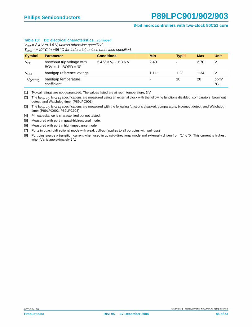
Philips Semiconductors P89LPC901/902/9038-bit microcontrollers with two-clock 80C51 core
[1] Typical ratings are not guaranteed. The values listed are at room temperature, 3 V.
[2] The IDD(oper), IPD(idle) specifications are measured using an external clock with the following functions disabled: comparators, brownoutdetect, and Watchdog timer (P89LPC901).
[3] The IDD(oper), IPD(idle) specifications are measured with the following functions disabled: comparators, brownout detect, and Watchdogtimer (P89LPC902, P89LPC903).
[4] Pin capacitance is characterized but not tested.
[5] Measured with port in quasi-bidirectional mode.
[6] Measured with port in high-impedance mode.
[7] Ports in quasi-bidirectional mode with weak pull-up (applies to all port pins with pull-ups)
[8] Port pins source a transition current when used in quasi-bidirectional mode and externally driven from ‘1’ to ‘0’. This current is highestwhen VIN is approximately 2 V.
VBO brownout trip voltage withBOV = ‘1’, BOPD = ‘0’
2.4 V < VDD < 3.6 V 2.40 - 2.70 V
VREF bandgap reference voltage 1.11 1.23 1.34 V
TC(VREF) bandgap temperaturecoefficient
- 10 20 ppm/°C
Table 13: DC electrical characteristics …continuedVDD = 2.4 V to 3.6 V, unless otherwise specified.Tamb = −40 °C to +85 °C for industrial, unless otherwise specified.
Symbol Parameter Conditions Min Typ [1] Max Unit
Product data Rev. 05 — 17 December 2004 45 of 53
9397 750 14465 © Koninklijke Philips Electronics N.V. 2004. All rights reserved.

Philips Semiconductors P89LPC901/902/9038-bit microcontrollers with two-clock 80C51 core
11. Dynamic characteristics
[1] Parameters are valid over operating temperature range unless otherwise specified. Parts are tested to 2 MHz, but are guaranteed tooperate down to 0 Hz.
Table 14: AC characteristicsVDD = 2.4 V to 3.6 V, unless otherwise specified.Tamb = −40 °C to +85 °C for industrial, unless otherwise specified.[1]
Symbol Parameter Conditions Variable clock fosc = 12 MHz Unit
Min Max Min Max
fRCOSC internal RC oscillator frequency(nominal f = 7.3728 MHz) trimmedto ± 1% at Tamb = 25 °C
7.189 7.557 7.189 7.557 MHz
fWDOSC internal Watchdog oscillatorfrequency (nominal f = 400 kHz)
320 520 320 520 kHz
Crystal oscillator (P89LPC901)
fosc oscillator frequency 0 12 - - MHz
tCLCL clock cycle see Figure 22 83 - - - ns
fCLKP CLKLP active frequency 0 8 - - MHz
Glitch filter
glitch rejection, P1.5/RST pin - 50 - 50 ns
signal acceptance, P1.5/RST pin 125 - 125 - ns
glitch rejection, any pin exceptP1.5/RST
- 15 - 15 ns
signal acceptance, any pin exceptP1.5/RST
50 - 50 - ns
External clock (P89LPC901)
tCHCX HIGH time see Figure 22 33 tCLCL − tCLCX 33 - ns
tCLCX LOW time see Figure 22 33 tCLCL − tCHCX 33 - ns
tCLCH rise time see Figure 22 - 8 - 8 ns
tCHCL fall time see Figure 22 - 8 - 8 ns
Shift register (UART mode 0 - P89LPC903)
tXLXL serial port clock cycle time see Figure 21 16 tCLCL - 1333 - ns
tQVXH output data set-up to clock risingedge
see Figure 21 13 tCLCL - 1083 - ns
tXHQX output data hold after clock risingedge
see Figure 21 - tCLCL + 20 - 103 ns
tXHDX input data hold after clock risingedge
see Figure 21 - 0 - 0 ns
tDVXH input data valid to clock rising edge see Figure 21 150 - 150 - ns
Product data Rev. 05 — 17 December 2004 46 of 53
9397 750 14465 © Koninklijke Philips Electronics N.V. 2004. All rights reserved.
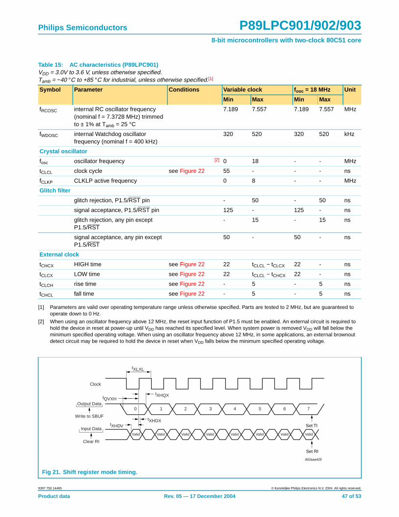
Philips Semiconductors P89LPC901/902/9038-bit microcontrollers with two-clock 80C51 core
[1] Parameters are valid over operating temperature range unless otherwise specified. Parts are tested to 2 MHz, but are guaranteed tooperate down to 0 Hz.
[2] When using an oscillator frequency above 12 MHz, the reset input function of P1.5 must be enabled. An external circuit is required tohold the device in reset at power-up until VDD has reached its specified level. When system power is removed VDD will fall below theminimum specified operating voltage. When using an oscillator frequency above 12 MHz, in some applications, an external brownoutdetect circuit may be required to hold the device in reset when VDD falls below the minimum specified operating voltage.
Table 15: AC characteristics (P89LPC901)VDD = 3.0V to 3.6 V, unless otherwise specified.Tamb = −40 °C to +85 °C for industrial, unless otherwise specified.[1]
Symbol Parameter Conditions Variable clock fosc = 18 MHz Unit
Min Max Min Max
fRCOSC internal RC oscillator frequency(nominal f = 7.3728 MHz) trimmedto ± 1% at Tamb = 25 °C
7.189 7.557 7.189 7.557 MHz
fWDOSC internal Watchdog oscillatorfrequency (nominal f = 400 kHz)
320 520 320 520 kHz
Crystal oscillator
fosc oscillator frequency [2] 0 18 - - MHz
tCLCL clock cycle see Figure 22 55 - - - ns
fCLKP CLKLP active frequency 0 8 - - MHz
Glitch filter
glitch rejection, P1.5/RST pin - 50 - 50 ns
signal acceptance, P1.5/RST pin 125 - 125 - ns
glitch rejection, any pin exceptP1.5/RST
- 15 - 15 ns
signal acceptance, any pin exceptP1.5/RST
50 - 50 - ns
External clock
tCHCX HIGH time see Figure 22 22 tCLCL − tCLCX 22 - ns
tCLCX LOW time see Figure 22 22 tCLCL − tCHCX 22 - ns
tCLCH rise time see Figure 22 - 5 - 5 ns
tCHCL fall time see Figure 22 - 5 - 5 ns
Fig 21. Shift register mode timing.
0 1 2 3 4 5 6 7
Valid Valid Valid Valid Valid Valid Valid Valid
tXLXL
002aaa425
Set TI
Set RI
tXHQXtQVXH
tXHDV
tXHDX
Clock
Output Data
Write to SBUF
Input Data
Clear RI
Product data Rev. 05 — 17 December 2004 47 of 53
9397 750 14465 © Koninklijke Philips Electronics N.V. 2004. All rights reserved.
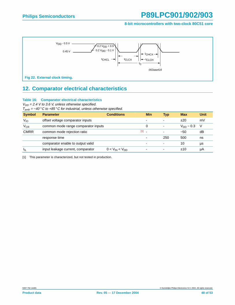
Philips Semiconductors P89LPC901/902/9038-bit microcontrollers with two-clock 80C51 core
12. Comparator electrical characteristics
[1] This parameter is characterized, but not tested in production.
Fig 22. External clock timing.
tCHCL tCLCX
tCHCX
tC
tCLCH
002aaa416
0.2 VDD + 0.9
0.2 VDD - 0.1 V
VDD - 0.5 V
0.45 V
Table 16: Comparator electrical characteristicsVDD = 2.4 V to 3.6 V, unless otherwise specified.Tamb = −40 °C to +85 °C for industrial, unless otherwise specified.
Symbol Parameter Conditions Min Typ Max Unit
VIO offset voltage comparator inputs - - ±20 mV
VCR common mode range comparator inputs 0 - VDD − 0.3 V
CMRR common mode rejection ratio [1] - - −50 dB
response time - 250 500 ns
comparator enable to output valid - - 10 µs
IIL input leakage current, comparator 0 < VIN < VDD - - ±10 µA
Product data Rev. 05 — 17 December 2004 48 of 53
9397 750 14465 © Koninklijke Philips Electronics N.V. 2004. All rights reserved.

Philips Semiconductors P89LPC901/902/9038-bit microcontrollers with two-clock 80C51 core
13. Package outline
Fig 23. SOT96-1 (SO8).
UNITA
max. A1 A2 A3 bp c D(1) E(2) (1)e HE L L p Q Zywv θ
REFERENCESOUTLINEVERSION
EUROPEANPROJECTION ISSUE DATE
IEC JEDEC JEITA
mm
inches
1.750.250.10
1.451.25
0.250.490.36
0.250.19
5.04.8
4.03.8
1.276.25.8
1.050.70.6
0.70.3 8
0
o
o
0.25 0.10.25
DIMENSIONS (inch dimensions are derived from the original mm dimensions)
Notes
1. Plastic or metal protrusions of 0.15 mm (0.006 inch) maximum per side are not included.
2. Plastic or metal protrusions of 0.25 mm (0.01 inch) maximum per side are not included.
1.00.4
SOT96-1
X
w M
θ
AA1
A2
bp
D
HE
Lp
Q
detail X
E
Z
e
c
L
v M A
(A )3
A
4
5
pin 1 index
1
8
y
076E03 MS-012
0.0690.0100.004
0.0570.049
0.010.0190.014
0.01000.0075
0.200.19
0.160.15
0.050.2440.228
0.0280.024
0.0280.012
0.010.010.041 0.0040.0390.016
0 2.5 5 mm
scale
SO8: plastic small outline package; 8 leads; body width 3.9 mm SOT96-1
99-12-2703-02-18
Product data Rev. 05 — 17 December 2004 49 of 53
9397 750 14465 © Koninklijke Philips Electronics N.V. 2004. All rights reserved.

Philips Semiconductors P89LPC901/902/9038-bit microcontrollers with two-clock 80C51 core
Fig 24. SOT97-1 (DIP8).
REFERENCESOUTLINEVERSION
EUROPEANPROJECTION ISSUE DATE
IEC JEDEC JEITA
SOT97-199-12-2703-02-13
UNIT Amax.
1 2 b1(1) (1) (1)
b2 c D E e M ZHL
mm
DIMENSIONS (inch dimensions are derived from the original mm dimensions)
A min.
A max. b
max.wMEe1
1.731.14
0.530.38
0.360.23
9.89.2
6.486.20
3.603.05
0.2542.54 7.628.257.80
10.08.3
1.154.2 0.51 3.2
inches 0.0680.045
0.0210.015
0.0140.009
1.070.89
0.0420.035
0.390.36
0.260.24
0.140.12
0.010.1 0.30.320.31
0.390.33
0.0450.17 0.02 0.13
b2
050G01 MO-001 SC-504-8
MH
c
(e )1
ME
A
L
seat
ing
plan
e
A1
w Mb1
e
D
A2
Z
8
1
5
4
b
E
0 5 10 mm
scale
Note
1. Plastic or metal protrusions of 0.25 mm (0.01 inch) maximum per side are not included.
pin 1 index
DIP8: plastic dual in-line package; 8 leads (300 mil) SOT97-1
Product data Rev. 05 — 17 December 2004 50 of 53
9397 750 14465 © Koninklijke Philips Electronics N.V. 2004. All rights reserved.
Philips Semiconductors P89LPC901/902/9038-bit microcontrollers with two-clock 80C51 core
14. Revision history
Table 17: Revision history
Rev Date CPCN Description
05 20041217 - Product data (9397 750 14465)
Modifications:
• Added 18 MHz information.
04 20031121 - Product data (9397 750 12293); ECN 853-2434 01-A14555 of 18 November 2003
03 20030929 - Product data (9397 750 12031); ECN 853-2434 30348 of 11 September 2003
02 20030731 - Product data (9397 750 11801); ECN 853-2434 30152 of 28 July 2003
01 20030602 - Preliminary data (9397 750 11494)
Product data Rev. 05 — 17 December 2004 51 of 53
9397 750 14465 © Koninklijke Philips Electronics N.V. 2004. All rights reserved.

Philips Semiconductors P89LPC901/902/9038-bit microcontrollers with two-clock 80C51 core
15. Data sheet status
[1] Please consult the most recently issued data sheet before initiating or completing a design.
[2] The product status of the device(s) described in this data sheet may have changed since this data sheet was published. The latest information is available on the Internet atURL http://www.semiconductors.philips.com.
[3] For data sheets describing multiple type numbers, the highest-level product status determines the data sheet status.
16. Definitions
Short-form specification — The data in a short-form specification isextracted from a full data sheet with the same type number and title. Fordetailed information see the relevant data sheet or data handbook.
Limiting values definition — Limiting values given are in accordance withthe Absolute Maximum Rating System (IEC 60134). Stress above one ormore of the limiting values may cause permanent damage to the device.These are stress ratings only and operation of the device at these or at anyother conditions above those given in the Characteristics sections of thespecification is not implied. Exposure to limiting values for extended periodsmay affect device reliability.
Application information — Applications that are described herein for anyof these products are for illustrative purposes only. Philips Semiconductorsmake no representation or warranty that such applications will be suitable forthe specified use without further testing or modification.
17. Disclaimers
Life support — These products are not designed for use in life supportappliances, devices, or systems where malfunction of these products canreasonably be expected to result in personal injury. Philips Semiconductorscustomers using or selling these products for use in such applications do soat their own risk and agree to fully indemnify Philips Semiconductors for anydamages resulting from such application.
Right to make changes — Philips Semiconductors reserves the right tomake changes in the products - including circuits, standard cells, and/orsoftware - described or contained herein in order to improve design and/orperformance. When the product is in full production (status ‘Production’),relevant changes will be communicated via a Customer Product/ProcessChange Notification (CPCN). Philips Semiconductors assumes noresponsibility or liability for the use of any of these products, conveys nolicence or title under any patent, copyright, or mask work right to theseproducts, and makes no representations or warranties that these products arefree from patent, copyright, or mask work right infringement, unless otherwisespecified.
Level Data sheet status [1] Product status [2][3] Definition
I Objective data Development This data sheet contains data from the objective specification for product development. PhilipsSemiconductors reserves the right to change the specification in any manner without notice.
II Preliminary data Qualification This data sheet contains data from the preliminary specification. Supplementary data will be publishedat a later date. Philips Semiconductors reserves the right to change the specification without notice, inorder to improve the design and supply the best possible product.
III Product data Production This data sheet contains data from the product specification. Philips Semiconductors reserves theright to make changes at any time in order to improve the design, manufacturing and supply. Relevantchanges will be communicated via a Customer Product/Process Change Notification (CPCN).
9397 750 14465 © Koninklijke Philips Electronics N.V. 2004. All rights reserved.
Product data Rev. 05 — 17 December 2004 52 of 53
Contact informationFor additional information, please visit http://www.semiconductors.philips.com .For sales office addresses, send e-mail to: [email protected] . Fax: +31 40 27 24825

© Koninklijke Philips Electronics N.V. 2004.Printed in the U.S.A.
All rights are reserved. Reproduction in whole or in part is prohibited without the priorwritten consent of the copyright owner.
The information presented in this document does not form part of any quotation orcontract, is believed to be accurate and reliable and may be changed without notice. Noliability will be accepted by the publisher for any consequence of its use. Publicationthereof does not convey nor imply any license under patent- or other industrial orintellectual property rights.
Date of release: 17 December 2004 Document order number: 9397 750 14465
Contents
Philips Semiconductors P89LPC901/902/9038-bit microcontrollers with two-clock 80C51 core
1 General description . . . . . . . . . . . . . . . . . . . . . . . . . . . 1
2 Features . . . . . . . . . . . . . . . . . . . . . . . . . . . . . . . . . . . . 12.1 Principal features . . . . . . . . . . . . . . . . . . . . . . . . . . . . 12.2 Additional features . . . . . . . . . . . . . . . . . . . . . . . . . . . 1
3 Ordering information. . . . . . . . . . . . . . . . . . . . . . . . . . 33.1 Ordering options . . . . . . . . . . . . . . . . . . . . . . . . . . . . 3
4 Block diagram . . . . . . . . . . . . . . . . . . . . . . . . . . . . . . . 4
5 Pinning information. . . . . . . . . . . . . . . . . . . . . . . . . . . 75.1 Pinning . . . . . . . . . . . . . . . . . . . . . . . . . . . . . . . . . . . . 75.2 Pin description . . . . . . . . . . . . . . . . . . . . . . . . . . . . . . 8
6 Logic symbols . . . . . . . . . . . . . . . . . . . . . . . . . . . . . . 12
7 Special function registers. . . . . . . . . . . . . . . . . . . . . 14
8 Functional description . . . . . . . . . . . . . . . . . . . . . . . 248.1 Enhanced CPU . . . . . . . . . . . . . . . . . . . . . . . . . . . . 248.2 Clocks . . . . . . . . . . . . . . . . . . . . . . . . . . . . . . . . . . . 248.2.1 Clock definitions . . . . . . . . . . . . . . . . . . . . . . . . . . . . 248.2.2 CPU clock (OSCCLK) . . . . . . . . . . . . . . . . . . . . . . . 248.2.3 Low speed oscillator option (P89LPC901) . . . . . . . . 248.2.4 Medium speed oscillator option (P89LPC901). . . . . 248.2.5 High speed oscillator option (P89LPC901) . . . . . . . 258.2.6 Clock output (P89LPC901) . . . . . . . . . . . . . . . . . . . 258.3 On-chip RC oscillator option . . . . . . . . . . . . . . . . . . 258.4 Watchdog oscillator option . . . . . . . . . . . . . . . . . . . . 258.5 External clock input option (P89LPC901) . . . . . . . . 258.6 CPU CLock (CCLK) wake-up delay . . . . . . . . . . . . . 278.7 CPU CLOCK (CCLK) modification: DIVM register . . 278.8 Low power select . . . . . . . . . . . . . . . . . . . . . . . . . . . 278.9 Memory organization . . . . . . . . . . . . . . . . . . . . . . . . 278.10 Data RAM arrangement . . . . . . . . . . . . . . . . . . . . . . 278.11 Interrupts . . . . . . . . . . . . . . . . . . . . . . . . . . . . . . . . . 278.11.1 External interrupt inputs . . . . . . . . . . . . . . . . . . . . . . 288.12 I/O ports . . . . . . . . . . . . . . . . . . . . . . . . . . . . . . . . . . 308.12.1 Port configurations . . . . . . . . . . . . . . . . . . . . . . . . . . 308.12.2 Quasi-bidirectional output configuration. . . . . . . . . . 318.12.3 Open-drain output configuration. . . . . . . . . . . . . . . . 318.12.4 Input-only configuration . . . . . . . . . . . . . . . . . . . . . . 318.12.5 Push-pull output configuration . . . . . . . . . . . . . . . . . 318.12.6 Port 0 analog functions . . . . . . . . . . . . . . . . . . . . . . 318.12.7 Additional port features . . . . . . . . . . . . . . . . . . . . . . 328.13 Power monitoring functions . . . . . . . . . . . . . . . . . . . 328.13.1 Brownout detection . . . . . . . . . . . . . . . . . . . . . . . . . 328.13.2 Power-on detection . . . . . . . . . . . . . . . . . . . . . . . . . 328.14 Power reduction modes . . . . . . . . . . . . . . . . . . . . . . 328.14.1 Idle mode . . . . . . . . . . . . . . . . . . . . . . . . . . . . . . . . . 338.14.2 Power-down mode . . . . . . . . . . . . . . . . . . . . . . . . . . 338.14.3 Total Power-down mode. . . . . . . . . . . . . . . . . . . . . . 338.15 Reset . . . . . . . . . . . . . . . . . . . . . . . . . . . . . . . . . . . . 338.16 Timers/counters 0 and 1 . . . . . . . . . . . . . . . . . . . . . 348.16.1 Mode 0 . . . . . . . . . . . . . . . . . . . . . . . . . . . . . . . . . . . 348.16.2 Mode 1 . . . . . . . . . . . . . . . . . . . . . . . . . . . . . . . . . . . 348.16.3 Mode 2 . . . . . . . . . . . . . . . . . . . . . . . . . . . . . . . . . . . 348.16.4 Mode 3 . . . . . . . . . . . . . . . . . . . . . . . . . . . . . . . . . . . 348.16.5 Mode 6 (P89LPC901) . . . . . . . . . . . . . . . . . . . . . . . 34
8.16.6 Timer overflow toggle output (P89LPC901) . . . . . . . 358.17 Real-Time clock/system timer. . . . . . . . . . . . . . . . . . 358.18 UART (P89LPC903) . . . . . . . . . . . . . . . . . . . . . . . . . 358.18.1 Mode 0 . . . . . . . . . . . . . . . . . . . . . . . . . . . . . . . . . . . 358.18.2 Mode 1 . . . . . . . . . . . . . . . . . . . . . . . . . . . . . . . . . . . 358.18.3 Mode 2 . . . . . . . . . . . . . . . . . . . . . . . . . . . . . . . . . . . 358.18.4 Mode 3 . . . . . . . . . . . . . . . . . . . . . . . . . . . . . . . . . . . 368.18.5 Baud rate generator and selection . . . . . . . . . . . . . . 368.18.6 Framing error . . . . . . . . . . . . . . . . . . . . . . . . . . . . . . 368.18.7 Break detect . . . . . . . . . . . . . . . . . . . . . . . . . . . . . . . 368.18.8 Double buffering . . . . . . . . . . . . . . . . . . . . . . . . . . . . 368.18.9 Transmit interrupts with double buffering
enabled (Modes 1, 2 and 3) . . . . . . . . . . . . . . . . . . . 378.18.10 The 9th bit (bit 8) in double buffering (Modes 1, 2 and
3) . . . . . . . . . . . . . . . . . . . . . . . . . . . . . . . . . . . . . . . 378.19 Analog comparators . . . . . . . . . . . . . . . . . . . . . . . . . 378.20 Internal reference voltage . . . . . . . . . . . . . . . . . . . . . 388.21 Comparator interrupt. . . . . . . . . . . . . . . . . . . . . . . . . 388.22 Comparator and power reduction modes . . . . . . . . . 388.23 Keypad interrupt (KBI) . . . . . . . . . . . . . . . . . . . . . . . 398.24 Watchdog timer. . . . . . . . . . . . . . . . . . . . . . . . . . . . . 398.25 Additional features . . . . . . . . . . . . . . . . . . . . . . . . . . 408.25.1 Software reset. . . . . . . . . . . . . . . . . . . . . . . . . . . . . . 408.25.2 Dual data pointers. . . . . . . . . . . . . . . . . . . . . . . . . . . 408.26 Flash program memory. . . . . . . . . . . . . . . . . . . . . . . 408.26.1 General description. . . . . . . . . . . . . . . . . . . . . . . . . . 408.26.2 Features . . . . . . . . . . . . . . . . . . . . . . . . . . . . . . . . . . 418.26.3 Flash organization . . . . . . . . . . . . . . . . . . . . . . . . . . 418.26.4 Flash programming and erasing . . . . . . . . . . . . . . . . 418.26.5 In-circuit programming (ICP). . . . . . . . . . . . . . . . . . . 418.26.6 In-application programming . . . . . . . . . . . . . . . . . . . 428.26.7 Using flash as data storage . . . . . . . . . . . . . . . . . . . 428.26.8 User configuration bytes . . . . . . . . . . . . . . . . . . . . . . 428.26.9 User sector security bytes . . . . . . . . . . . . . . . . . . . . 42
9 Limiting values . . . . . . . . . . . . . . . . . . . . . . . . . . . . . . 43
10 Static characteristics . . . . . . . . . . . . . . . . . . . . . . . . . 44
11 Dynamic characteristics . . . . . . . . . . . . . . . . . . . . . . 46
12 Comparator electrical characteristics . . . . . . . . . . . 48
13 Package outline . . . . . . . . . . . . . . . . . . . . . . . . . . . . . 49
14 Revision history . . . . . . . . . . . . . . . . . . . . . . . . . . . . . 51
15 Data sheet status . . . . . . . . . . . . . . . . . . . . . . . . . . . . 52
16 Definitions. . . . . . . . . . . . . . . . . . . . . . . . . . . . . . . . . . 52
17 Disclaimers . . . . . . . . . . . . . . . . . . . . . . . . . . . . . . . . . 52