P89C51RB2/P89C51RC2/P89C51RD2 80C51 8-bit Flash ...P89C51RB2/P89C51RC2/ P89C51RD2 80C51 8-bit Flash...
52
Philips Semiconductors P89C51RB2/P89C51RC2/P89C51RD2 80C51 8-bit Flash microcontroller family 16KB/32KB/64KB ISP/IAP Flash with 512B/512B/1KB RAM Preliminary specification Supersedes data of 2001 Jan 11 IC28 Data Handbook 2001 Jun 27 INTEGRATED CIRCUITS
Transcript of P89C51RB2/P89C51RC2/P89C51RD2 80C51 8-bit Flash ...P89C51RB2/P89C51RC2/ P89C51RD2 80C51 8-bit Flash...
������ ����������
P89C51RB2/P89C51RC2/P89C51RD280C51 8-bit Flash microcontroller family16KB/32KB/64KB ISP/IAP Flash with 512B/512B/1KB RAM
Preliminary specificationSupersedes data of 2001 Jan 11IC28 Data Handbook
2001 Jun 27
INTEGRATED CIRCUITS
Philips Semiconductors Preliminary data
P89C51RB2/P89C51RC2/P89C51RD2
80C51 8-bit Flash microcontroller family16KB/32KB/64KB ISP/IAP Flash with 512B/512B/1KB RAM
22001 Jun 27
DESCRIPTIONThe P89C51RB2/RC2/RD2 device contains a non-volatile16KB/32KB/64KB Flash program memory that is both parallelprogrammable and serial In-System and In-ApplicationProgrammable. In-System Programming (ISP) allows the user todownload new code while the microcontroller sits in the application.In-Application Programming (IAP) means that the microcontrollerfetches new program code and reprograms itself while in thesystem. This allows for remote programming over a modem link.A default serial loader (boot loader) program in ROM allows serialIn-System programming of the Flash memory via the UART withoutthe need for a loader in the Flash code. For In-ApplicationProgramming, the user program erases and reprograms the Flashmemory by use of standard routines contained in ROM.
This device executes one machine cycle in 6 clock cycles, henceproviding twice the speed of a conventional 80C51. An OTPconfiguration bit lets the user select conventional 12 clock timingif desired.
This device is a Single-Chip 8-Bit Microcontroller manufactured inadvanced CMOS process and is a derivative of the 80C51microcontroller family. The instruction set is 100% compatible withthe 80C51 instruction set.
The device also has four 8-bit I/O ports, three 16-bit timer/eventcounters, a multi-source, four-priority-level, nested interrupt structure,an enhanced UART and on-chip oscillator and timing circuits.
The added features of the P89C51RB2/RC2/RD2 makes it apowerful microcontroller for applications that require pulse widthmodulation, high-speed I/O and up/down counting capabilities suchas motor control.
FEATURES• 80C51 Central Processing Unit
• On-chip Flash Program Memory with In-System Programming(ISP) and In-Application Programming (IAP) capability
• Boot ROM contains low level Flash programming routines fordownloading via the UART
• Can be programmed by the end-user application (IAP)
• Parallel programming with 87C51 compatible hardware interfaceto programmer
• 6 clocks per machine cycle operation (standard)
• 12 clocks per machine cycle operation (optional)
• Speed up to 20 MHz with 6 clock cycles per machine cycle(40 MHz equivalent performance); up to 33 MHz with 12 clocksper machine cycle
• Fully static operation
• RAM expandable externally to 64 kbytes
• 4 level priority interrupt
• 7 interrupt sources
• Four 8-bit I/O ports
• Full-duplex enhanced UART
– Framing error detection
– Automatic address recognition
• Power control modes
– Clock can be stopped and resumed
– Idle mode
– Power down mode
• Programmable clock out
• Second DPTR register
• Asynchronous port reset
• Low EMI (inhibit ALE)
• Programmable Counter Array (PCA)
– PWM
– Capture/compare
Philips Semiconductors Preliminary data
P89C51RB2/P89C51RC2/P89C51RD2
80C51 8-bit Flash microcontroller family16KB/32KB/64KB ISP/IAP Flash with 512B/512B/1KB RAM
2001 Jun 27 3
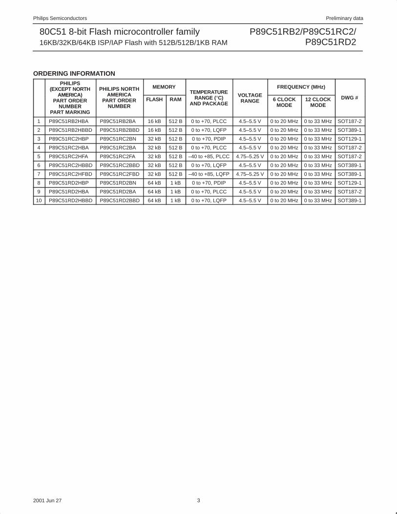
ORDERING INFORMATIONPHILIPS
(EXCEPT NORTHAMERICA)
PHILIPS NORTHAMERICA
MEMORYTEMPERATURE
VOLTAGE
FREQUENCY (MHz)
AMERICA)PART ORDER
NUMBERPART MARKING
AMERICAPART ORDER
NUMBERFLASH RAM RANGE (°C)
AND PACKAGE
VOLTAGERANGE 6 CLOCK
MODE12 CLOCK
MODEDWG #
1 P89C51RB2HBA P89C51RB2BA 16 kB 512 B 0 to +70, PLCC 4.5–5.5 V 0 to 20 MHz 0 to 33 MHz SOT187-2
2 P89C51RB2HBBD P89C51RB2BBD 16 kB 512 B 0 to +70, LQFP 4.5–5.5 V 0 to 20 MHz 0 to 33 MHz SOT389-1
3 P89C51RC2HBP P89C51RC2BN 32 kB 512 B 0 to +70, PDIP 4.5–5.5 V 0 to 20 MHz 0 to 33 MHz SOT129-1
4 P89C51RC2HBA P89C51RC2BA 32 kB 512 B 0 to +70, PLCC 4.5–5.5 V 0 to 20 MHz 0 to 33 MHz SOT187-2
5 P89C51RC2HFA P89C51RC2FA 32 kB 512 B –40 to +85, PLCC 4.75–5.25 V 0 to 20 MHz 0 to 33 MHz SOT187-2
6 P89C51RC2HBBD P89C51RC2BBD 32 kB 512 B 0 to +70, LQFP 4.5–5.5 V 0 to 20 MHz 0 to 33 MHz SOT389-1
7 P89C51RC2HFBD P89C51RC2FBD 32 kB 512 B –40 to +85, LQFP 4.75–5.25 V 0 to 20 MHz 0 to 33 MHz SOT389-1
8 P89C51RD2HBP P89C51RD2BN 64 kB 1 kB 0 to +70, PDIP 4.5–5.5 V 0 to 20 MHz 0 to 33 MHz SOT129-1
9 P89C51RD2HBA P89C51RD2BA 64 kB 1 kB 0 to +70, PLCC 4.5–5.5 V 0 to 20 MHz 0 to 33 MHz SOT187-2
10 P89C51RD2HBBD P89C51RD2BBD 64 kB 1 kB 0 to +70, LQFP 4.5–5.5 V 0 to 20 MHz 0 to 33 MHz SOT389-1
Philips Semiconductors Preliminary data
P89C51RB2/P89C51RC2/P89C51RD2
80C51 8-bit Flash microcontroller family16KB/32KB/64KB ISP/IAP Flash with 512B/512B/1KB RAM
2001 Jun 27 4
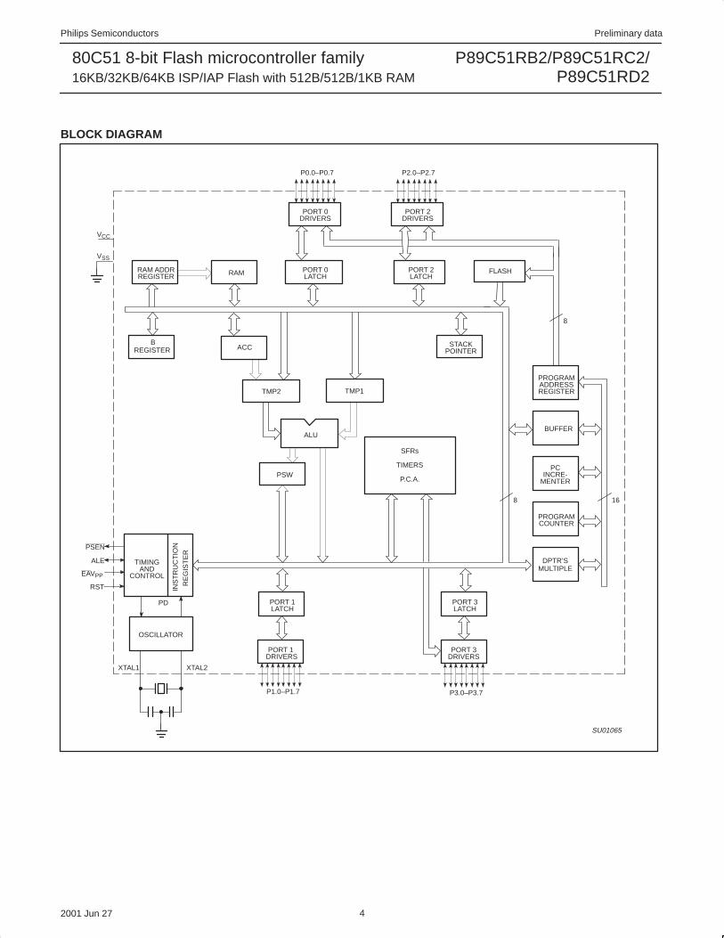
BLOCK DIAGRAM
SU01065
PSEN
EAVPP
ALE
RST
XTAL1 XTAL2
VCC
VSS
PORT 0DRIVERS
PORT 2DRIVERS
RAM ADDRREGISTER RAM PORT 0
LATCHPORT 2LATCH
FLASH
REGISTERB
ACC STACKPOINTER
TMP2 TMP1
ALU
TIMINGAND
CONTROL
INS
TR
UC
TIO
N
RE
GIS
TE
R
PD
OSCILLATOR
PSW
PORT 1LATCH
PORT 3LATCH
PORT 1 DRIVERS
PORT 3DRIVERS
PROGRAMADDRESSREGISTER
BUFFER
PCINCRE-
MENTER
PROGRAMCOUNTER
DPTR’SMULTIPLE
P1.0–P1.7 P3.0–P3.7
P0.0–P0.7 P2.0–P2.7
SFRs
TIMERS
P.C.A.
8
8 16
Philips Semiconductors Preliminary data
P89C51RB2/P89C51RC2/P89C51RD2
80C51 8-bit Flash microcontroller family16KB/32KB/64KB ISP/IAP Flash with 512B/512B/1KB RAM
2001 Jun 27 5
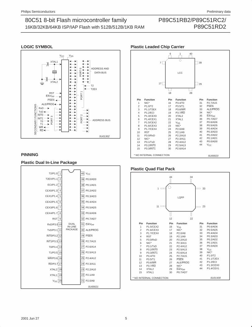
LOGIC SYMBOL
PO
RT
0P
OR
T 1
PO
RT
2
PO
RT
3
ADDRESS AND
DATA BUS
ADDRESS BUS
T2T2EX
RxD
TxDINT0
INT1T0T1
WRRD
SE
CO
ND
AR
Y F
UN
CT
ION
S
RSTEA/VPP
PSEN
ALE/PROG
VSSVCC
XTAL1
XTAL2
SU01302
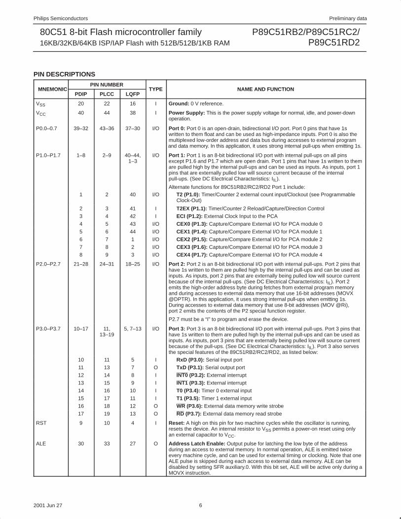
PINNING
Plastic Dual In-Line Package
1
2
3
4
5
6
7
8
9
10
11
12
13
14
15
16
17
18
19
20 21
22
23
24
25
26
27
28
29
30
31
32
33
34
35
36
37
38
39
40T2/P1.0
T2EX/P1.1
ECI/P1.2
CEX0/P1.3
CEX1/P1.4
CEX2/P1.5
CEX3/P1.6
RST
RxD/P3.0
TxD/P3.1
INT0/P3.2
INT1/P3.3
T0/P3.4
T1/P3.5
CEX4/P1.7
WR/P3.6
RD/P3.7
XTAL2
XTAL1
VSS P2.0/A8
P2.1/A9
P2.2/A10
P2.3/A11
P2.4/A12
P2.5/A13
P2.6/A14
P2.7/A15
PSEN
ALE/PROG
EA/VPP
P0.7/AD7
P0.6/AD6
P0.5/AD5
P0.4/AD4
P0.3/AD3
P0.2/AD2
P0.1/AD1
P0.0/AD0
VCC
DUALIN-LINE
PACKAGE
SU00021
Plastic Leaded Chip Carrier
LCC
6 1 40
7
17
39
29
18 28
Pin Function1 NIC*2 P1.0/T23 P1.1/T2EX4 P1.2/ECI5 P1.3/CEX06 P1.4/CEX17 P1.5/CEX28 P1.6/CEX39 P1.7/CEX4
10 RST11 P3.0/RxD12 NIC*13 P3.1/TxD14 P3.2/INT015 P3.3/INT1
Pin Function16 P3.4/T017 P3.5/T118 P3.6/WR19 P3.7/RD20 XTAL221 XTAL122 VSS23 NIC*24 P2.0/A825 P2.1/A926 P2.2/A1027 P2.3/A1128 P2.4/A1229 P2.5/A1330 P2.6/A14
Pin Function31 P2.7/A1532 PSEN33 ALE/PROG34 NIC*35 EA/VPP36 P0.7/AD737 P0.6/AD638 P0.5/AD539 P0.4/AD440 P0.3/AD341 P0.2/AD242 P0.1/AD143 P0.0/AD044 VCC
SU00023* NO INTERNAL CONNECTION
Plastic Quad Flat Pack
LQFP
44 34
1
11
33
23
12 22
Pin Function1 P1.5/CEX22 P1.6/CEX33 P1.7/CEX44 RST5 P3.0/RxD6 NIC*7 P3.1/TxD8 P3.2/INT09 P3.3/INT1
10 P3.4/T011 P3.5/T112 P3.6/WR13 P3.7/RD14 XTAL215 XTAL1
Pin Function16 VSS17 NIC*18 P2.0/A819 P2.1/A920 P2.2/A1021 P2.3/A1122 P2.4/A1223 P2.5/A1324 P2.6/A1425 P2.7/A1526 PSEN27 ALE/PROG28 NIC*29 EA/VPP30 P0.7/AD7
Pin Function31 P0.6/AD632 P0.5/AD533 P0.4/AD434 P0.3/AD335 P0.2/AD236 P0.1/AD137 P0.0/AD038 VCC39 NIC*40 P1.0/T241 P1.1/T2EX42 P1.2/ECI43 P1.3/CEX044 P1.4/CEX1
SU01400* NO INTERNAL CONNECTION
Philips Semiconductors Preliminary data
P89C51RB2/P89C51RC2/P89C51RD2
80C51 8-bit Flash microcontroller family16KB/32KB/64KB ISP/IAP Flash with 512B/512B/1KB RAM
2001 Jun 27 6
PIN DESCRIPTIONS
MNEMONICPIN NUMBER
TYPE NAME AND FUNCTIONMNEMONICPDIP PLCC LQFP
TYPE NAME AND FUNCTION
VSS 20 22 16 I Ground: 0 V reference.
VCC 40 44 38 I Power Supply: This is the power supply voltage for normal, idle, and power-downoperation.
P0.0–0.7 39–32 43–36 37–30 I/O Port 0: Port 0 is an open-drain, bidirectional I/O port. Port 0 pins that have 1swritten to them float and can be used as high-impedance inputs. Port 0 is also themultiplexed low-order address and data bus during accesses to external programand data memory. In this application, it uses strong internal pull-ups when emitting 1s.
P1.0–P1.7 1–8 2–9 40–44,1–3
I/O Port 1: Port 1 is an 8-bit bidirectional I/O port with internal pull-ups on all pinsexcept P1.6 and P1.7 which are open drain. Port 1 pins that have 1s written to themare pulled high by the internal pull-ups and can be used as inputs. As inputs, port 1pins that are externally pulled low will source current because of the internalpull-ups. (See DC Electrical Characteristics: IIL).
Alternate functions for 89C51RB2/RC2/RD2 Port 1 include:1 2 40 I/O T2 (P1.0): Timer/Counter 2 external count input/Clockout (see Programmable
Clock-Out)
2 3 41 I T2EX (P1.1): Timer/Counter 2 Reload/Capture/Direction Control
3 4 42 I ECI (P1.2): External Clock Input to the PCA
4 5 43 I/O CEX0 (P1.3): Capture/Compare External I/O for PCA module 0
5 6 44 I/O CEX1 (P1.4): Capture/Compare External I/O for PCA module 1
6 7 1 I/O CEX2 (P1.5): Capture/Compare External I/O for PCA module 2
7 8 2 I/O CEX3 (P1.6): Capture/Compare External I/O for PCA module 3
8 9 3 I/O CEX4 (P1.7): Capture/Compare External I/O for PCA module 4
P2.0–P2.7 21–28 24–31 18–25 I/O Port 2: Port 2 is an 8-bit bidirectional I/O port with internal pull-ups. Port 2 pins thathave 1s written to them are pulled high by the internal pull-ups and can be used asinputs. As inputs, port 2 pins that are externally being pulled low will source currentbecause of the internal pull-ups. (See DC Electrical Characteristics: IIL). Port 2emits the high-order address byte during fetches from external program memoryand during accesses to external data memory that use 16-bit addresses (MOVX@DPTR). In this application, it uses strong internal pull-ups when emitting 1s.During accesses to external data memory that use 8-bit addresses (MOV @Ri),port 2 emits the contents of the P2 special function register.
P2.7 must be a “I” to program and erase the device.
P3.0–P3.7 10–17 11,13–19
5, 7–13 I/O Port 3: Port 3 is an 8-bit bidirectional I/O port with internal pull-ups. Port 3 pins thathave 1s written to them are pulled high by the internal pull-ups and can be used asinputs. As inputs, port 3 pins that are externally being pulled low will source currentbecause of the pull-ups. (See DC Electrical Characteristics: IIL). Port 3 also servesthe special features of the 89C51RB2/RC2/RD2, as listed below:
10 11 5 I RxD (P3.0): Serial input port
11 13 7 O TxD (P3.1): Serial output port
12 14 8 I INT0 (P3.2): External interrupt
13 15 9 I INT1 (P3.3): External interrupt
14 16 10 I T0 (P3.4): Timer 0 external input
15 17 11 I T1 (P3.5): Timer 1 external input
16 18 12 O WR (P3.6): External data memory write strobe
17 19 13 O RD (P3.7): External data memory read strobe
RST 9 10 4 I Reset: A high on this pin for two machine cycles while the oscillator is running,resets the device. An internal resistor to VSS permits a power-on reset using onlyan external capacitor to VCC.
ALE 30 33 27 O Address Latch Enable: Output pulse for latching the low byte of the addressduring an access to external memory. In normal operation, ALE is emitted twiceevery machine cycle, and can be used for external timing or clocking. Note that oneALE pulse is skipped during each access to external data memory. ALE can bedisabled by setting SFR auxiliary.0. With this bit set, ALE will be active only during aMOVX instruction.
Philips Semiconductors Preliminary data
P89C51RB2/P89C51RC2/P89C51RD2
80C51 8-bit Flash microcontroller family16KB/32KB/64KB ISP/IAP Flash with 512B/512B/1KB RAM
2001 Jun 27 7
MNEMONIC NAME AND FUNCTIONTYPEPIN NUMBER
MNEMONIC NAME AND FUNCTIONTYPELQFPPLCCPDIP
PSEN 29 32 26 O Program Store Enable: The read strobe to external program memory. Whenexecuting code from the external program memory, PSEN is activated twice eachmachine cycle, except that two PSEN activations are skipped during each accessto external data memory. PSEN is not activated during fetches from internalprogram memory.
EA/VPP 31 35 29 I External Access Enable/Programming Supply Voltage: EA must be externallyheld low to enable the device to fetch code from external program memorylocations. If EA is held high, the device executes from internal program memory.The value on the EA pin is latched when RST is released and any subsequentchanges have no effect. This pin also receives the programming supply voltage(VPP) during Flash programming.
XTAL1 19 21 15 I Crystal 1: Input to the inverting oscillator amplifier and input to the internal clockgenerator circuits.
XTAL2 18 20 14 O Crystal 2: Output from the inverting oscillator amplifier.
NOTE:To avoid “latch-up” effect at power-on, the voltage on any pin (other than VPP) must not be higher than VCC + 0.5 V or less than VSS – 0.5 V.
Philips Semiconductors Preliminary data
P89C51RB2/P89C51RC2/P89C51RD2
80C51 8-bit Flash microcontroller family16KB/32KB/64KB ISP/IAP Flash with 512B/512B/1KB RAM
2001 Jun 27 8
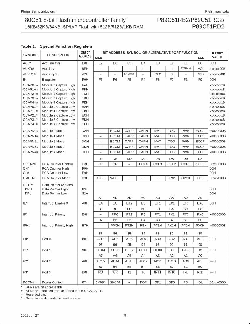
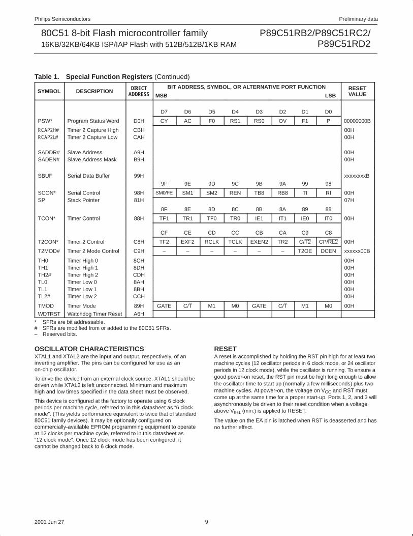
Table 1. Special Function Registers
SYMBOL DESCRIPTIONDIRECT
ADDRESSBIT ADDRESS, SYMBOL, OR ALTERNATIVE PORT FUNCTION
MSB LSBRESETVALUE
ACC* Accumulator E0H E7 E6 E5 E4 E3 E2 E1 E0 00H
AUXR# Auxiliary 8EH – – – – – – EXTRAM AO xxxxxx00B
AUXR1# Auxiliary 1 A2H – – ENBOOT – GF2 0 – DPS xxxxxxx0B
B* B register F0H F7 F6 F5 F4 F3 F2 F1 F0 00H
CCAP0H# Module 0 Capture High FAH xxxxxxxxBCCAP1H# Module 1 Capture High FBH xxxxxxxxBCCAP2H# Module 2 Capture High FCH xxxxxxxxBCCAP3H# Module 3 Capture High FDH xxxxxxxxBCCAP4H# Module 4 Capture High FEH xxxxxxxxBCCAP0L# Module 0 Capture Low EAH xxxxxxxxBCCAP1L# Module 1 Capture Low EBH xxxxxxxxBCCAP2L# Module 2 Capture Low ECH xxxxxxxxBCCAP3L# Module 3 Capture Low EDH xxxxxxxxBCCAP4L# Module 4 Capture Low EEH xxxxxxxxB
CCAPM0# Module 0 Mode DAH – ECOM CAPP CAPN MAT TOG PWM ECCF x0000000B
CCAPM1# Module 1 Mode DBH – ECOM CAPP CAPN MAT TOG PWM ECCF x0000000B
CCAPM2# Module 2 Mode DCH – ECOM CAPP CAPN MAT TOG PWM ECCF x0000000B
CCAPM3# Module 3 Mode DDH – ECOM CAPP CAPN MAT TOG PWM ECCF x0000000B
CCAPM4# Module 4 Mode DEH – ECOM CAPP CAPN MAT TOG PWM ECCF x0000000B
DF DE DD DC DB DA D9 D8
CCON*# PCA Counter Control D8H CF CR – CCF4 CCF3 CCF2 CCF1 CCF0 00x00000BCH# PCA Counter High F9H 00HCL# PCA Counter Low E9H 00H
CMOD# PCA Counter Mode D9H CIDL WDTE – – – CPS1 CPS0 ECF 00xxx000B
DPTR: Data Pointer (2 bytes)DPH Data Pointer High 83H 00HDPL Data Pointer Low 82H 00H
AF AE AD AC AB AA A9 A8
IE* Interrupt Enable 0 A8H EA EC ET2 ES ET1 EX1 ET0 EX0 00H
BF BE BD BC BB BA B9 B8
IP* Interrupt Priority B8H – PPC PT2 PS PT1 PX1 PT0 PX0 x0000000B
B7 B6 B5 B4 B3 B2 B1 B0
IPH# Interrupt Priority High B7H – PPCH PT2H PSH PT1H PX1H PT0H PX0H x0000000B
87 86 85 84 83 82 81 80
P0* Port 0 80H AD7 AD6 AD5 AD4 AD3 AD2 AD1 AD0 FFH
97 96 95 94 93 92 91 90
P1* Port 1 90H CEX4 CEX3 CEX2 CEX1 CEX0 ECI T2EX T2 FFH
A7 A6 A5 A4 A3 A2 A1 A0
P2* Port 2 A0H AD15 AD14 AD13 AD12 AD11 AD10 AD9 AD8 FFH
B7 B6 B5 B4 B3 B2 B1 B0
P3* Port 3 B0H RD WR T1 T0 INT1 INT0 TxD RxD FFH
PCON#1 Power Control 87H SMOD1 SMOD0 – POF GF1 GF0 PD IDL 00xxx000B
* SFRs are bit addressable.# SFRs are modified from or added to the 80C51 SFRs.– Reserved bits.1. Reset value depends on reset source.
Philips Semiconductors Preliminary data
P89C51RB2/P89C51RC2/P89C51RD2
80C51 8-bit Flash microcontroller family16KB/32KB/64KB ISP/IAP Flash with 512B/512B/1KB RAM
2001 Jun 27 9
Table 1. Special Function Registers (Continued)
SYMBOL DESCRIPTION DIRECTADDRESS
BIT ADDRESS, SYMBOL, OR ALTERNATIVE PORT FUNCTION
MSB LSBRESETVALUE
D7 D6 D5 D4 D3 D2 D1 D0
PSW* Program Status Word D0H CY AC F0 RS1 RS0 OV F1 P 00000000B
RCAP2H# Timer 2 Capture High CBH 00HRCAP2L# Timer 2 Capture Low CAH 00H
SADDR# Slave Address A9H 00HSADEN# Slave Address Mask B9H 00H
SBUF Serial Data Buffer 99H xxxxxxxxB
9F 9E 9D 9C 9B 9A 99 98
SCON* Serial Control 98H SM0/FE SM1 SM2 REN TB8 RB8 TI RI 00HSP Stack Pointer 81H 07H
8F 8E 8D 8C 8B 8A 89 88
TCON* Timer Control 88H TF1 TR1 TF0 TR0 IE1 IT1 IE0 IT0 00H
CF CE CD CC CB CA C9 C8
T2CON* Timer 2 Control C8H TF2 EXF2 RCLK TCLK EXEN2 TR2 C/T2 CP/RL2 00H
T2MOD# Timer 2 Mode Control C9H – – – – – – T2OE DCEN xxxxxx00B
TH0 Timer High 0 8CH 00HTH1 Timer High 1 8DH 00HTH2# Timer High 2 CDH 00HTL0 Timer Low 0 8AH 00HTL1 Timer Low 1 8BH 00HTL2# Timer Low 2 CCH 00H
TMOD Timer Mode 89H GATE C/T M1 M0 GATE C/T M1 M0 00H
WDTRST Watchdog Timer Reset A6H
* SFRs are bit addressable.# SFRs are modified from or added to the 80C51 SFRs.– Reserved bits.
OSCILLATOR CHARACTERISTICSXTAL1 and XTAL2 are the input and output, respectively, of aninverting amplifier. The pins can be configured for use as anon-chip oscillator.
To drive the device from an external clock source, XTAL1 should bedriven while XTAL2 is left unconnected. Minimum and maximumhigh and low times specified in the data sheet must be observed.
This device is configured at the factory to operate using 6 clockperiods per machine cycle, referred to in this datasheet as “6 clockmode”. (This yields performance equivalent to twice that of standard80C51 family devices). It may be optionally configured oncommercially-available EPROM programming equipment to operateat 12 clocks per machine cycle, referred to in this datasheet as“12 clock mode”. Once 12 clock mode has been configured, itcannot be changed back to 6 clock mode.
RESETA reset is accomplished by holding the RST pin high for at least twomachine cycles (12 oscillator periods in 6 clock mode, or 24 oscillatorperiods in 12 clock mode), while the oscillator is running. To ensure agood power-on reset, the RST pin must be high long enough to allowthe oscillator time to start up (normally a few milliseconds) plus twomachine cycles. At power-on, the voltage on VCC and RST mustcome up at the same time for a proper start-up. Ports 1, 2, and 3 willasynchronously be driven to their reset condition when a voltageabove VIH1 (min.) is applied to RESET.
The value on the EA pin is latched when RST is deasserted and hasno further effect.
Philips Semiconductors Preliminary data
P89C51RB2/P89C51RC2/P89C51RD2
80C51 8-bit Flash microcontroller family16KB/32KB/64KB ISP/IAP Flash with 512B/512B/1KB RAM
2001 Jun 27 10
LOW POWER MODESStop Clock ModeThe static design enables the clock speed to be reduced down to0 MHz (stopped). When the oscillator is stopped, the RAM andSpecial Function Registers retain their values. This mode allowsstep-by-step utilization and permits reduced system powerconsumption by lowering the clock frequency down to any value. Forlowest power consumption the Power Down mode is suggested.
Idle ModeIn the idle mode (see Table 2), the CPU puts itself to sleep while allof the on-chip peripherals stay active. The instruction to invoke theidle mode is the last instruction executed in the normal operatingmode before the idle mode is activated. The CPU contents, theon-chip RAM, and all of the special function registers remain intactduring this mode. The idle mode can be terminated either by anyenabled interrupt (at which time the process is picked up at theinterrupt service routine and continued), or by a hardware resetwhich starts the processor in the same manner as a power-on reset.
Power-Down ModeTo save even more power, a Power Down mode (see Table 2) canbe invoked by software. In this mode, the oscillator is stopped andthe instruction that invoked Power Down is the last instructionexecuted. The on-chip RAM and Special Function Registers retaintheir values down to 2.0 V and care must be taken to return VCC tothe minimum specified operating voltages before the Power DownMode is terminated.
Either a hardware reset or external interrupt can be used to exit fromPower Down. Reset redefines all the SFRs but does not change theon-chip RAM. An external interrupt allows both the SFRs and theon-chip RAM to retain their values.
To properly terminate Power Down, the reset or external interruptshould not be executed before VCC is restored to its normaloperating level and must be held active long enough for theoscillator to restart and stabilize (normally less than 10 ms).
With an external interrupt, INT0 and INT1 must be enabled andconfigured as level-sensitive. Holding the pin low restarts the oscillatorbut bringing the pin back high completes the exit. Once the interruptis serviced, the next instruction to be executed after RETI will be theone following the instruction that put the device into Power Down.
POWER OFF FLAGThe Power Off Flag (POF) is set by on-chip circuitry when the VCClevel on the P89C51RB2/RC2/RD2 rises from 0 to 5 V. The POF bitcan be set or cleared by software allowing a user to determine if thereset is the result of a power-on or a warm start after powerdown.The VCC level must remain above 3 V for the POF to remainunaffected by the VCC level.
Design Consideration• When the idle mode is terminated by a hardware reset, the device
normally resumes program execution, from where it left off, up totwo machine cycles before the internal reset algorithm takescontrol. On-chip hardware inhibits access to internal RAM in thisevent, but access to the port pins is not inhibited. To eliminate the
possibility of an unexpected write when Idle is terminated by reset,the instruction following the one that invokes Idle should not beone that writes to a port pin or to external memory.
ONCE ModeThe ONCE (“On-Circuit Emulation”) Mode facilitates testing anddebugging of systems without the device having to be removed fromthe circuit. The ONCE Mode is invoked by:
1. Pull ALE low while the device is in reset and PSEN is high;
2. Hold ALE low as RST is deactivated.
While the device is in ONCE Mode, the Port 0 pins go into a floatstate, and the other port pins and ALE and PSEN are weakly pulledhigh. The oscillator circuit remains active. While the device is in thismode, an emulator or test CPU can be used to drive the circuit.Normal operation is restored when a normal reset is applied.
Programmable Clock-OutA 50% duty cycle clock can be programmed to come out on P1.0.This pin, besides being a regular I/O pin, has two alternatefunctions. It can be programmed:
1. to input the external clock for Timer/Counter 2, or
2. to output a 50% duty cycle clock ranging from 122 Hz to 8 MHz ata 16 MHz operating frequency (61 Hz to 4 MHz in 12 clock mode).
To configure the Timer/Counter 2 as a clock generator, bit C/T2 (inT2CON) must be cleared and bit T20E in T2MOD must be set. BitTR2 (T2CON.2) also must be set to start the timer.
The Clock-Out frequency depends on the oscillator frequency andthe reload value of Timer 2 capture registers (RCAP2H, RCAP2L)as shown in this equation:
Oscillator Frequencyn � (65536 � RCAP2H, RCAP2L)
n = 2 in 6 clock mode4 in 12 clock mode
Where (RCAP2H,RCAP2L) = the content of RCAP2H and RCAP2Ltaken as a 16-bit unsigned integer.
In the Clock-Out mode Timer 2 roll-overs will not generate aninterrupt. This is similar to when it is used as a baud-rate generator.It is possible to use Timer 2 as a baud-rate generator and a clockgenerator simultaneously. Note, however, that the baud-rate and theClock-Out frequency will be the same.
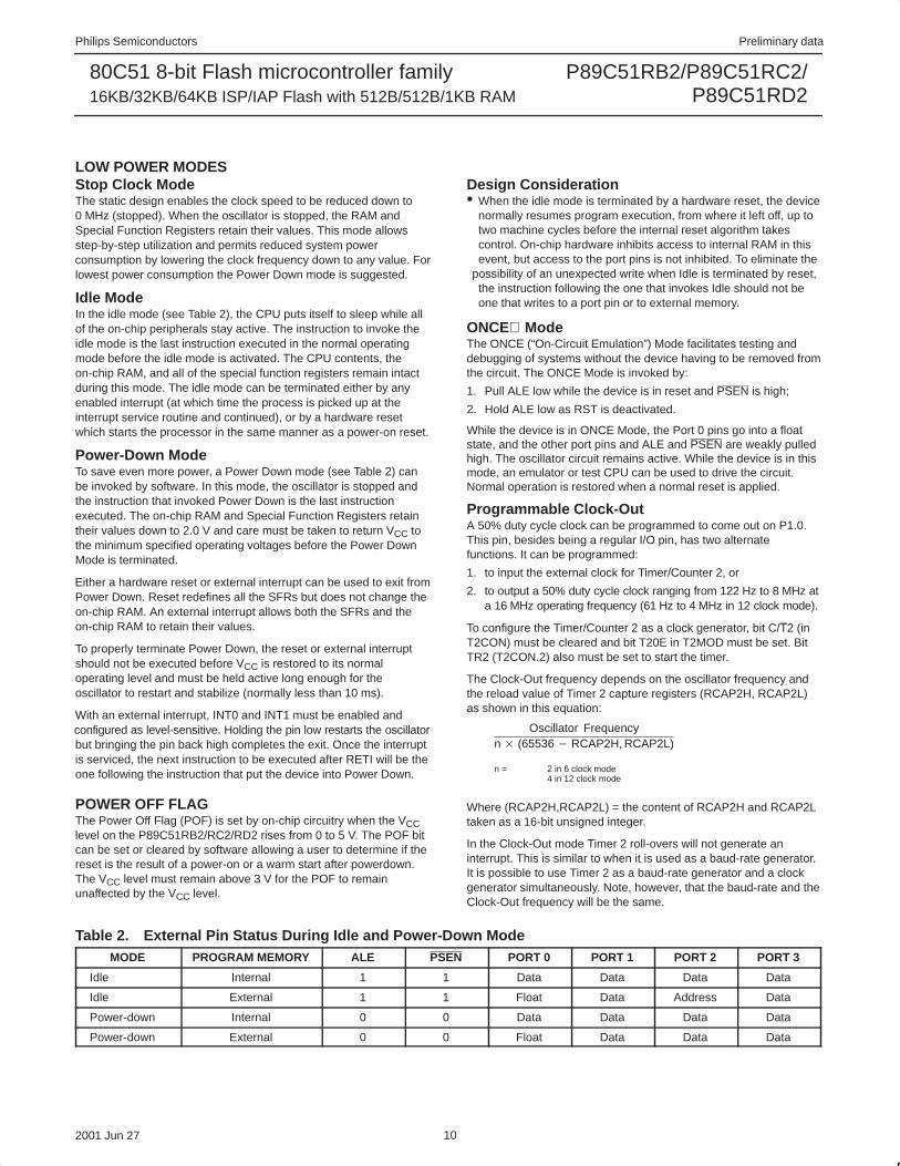
Table 2. External Pin Status During Idle and Power-Down ModeMODE PROGRAM MEMORY ALE PSEN PORT 0 PORT 1 PORT 2 PORT 3
Idle Internal 1 1 Data Data Data Data
Idle External 1 1 Float Data Address Data
Power-down Internal 0 0 Data Data Data Data
Power-down External 0 0 Float Data Data Data
Philips Semiconductors Preliminary data
P89C51RB2/P89C51RC2/P89C51RD2
80C51 8-bit Flash microcontroller family16KB/32KB/64KB ISP/IAP Flash with 512B/512B/1KB RAM
2001 Jun 27 11
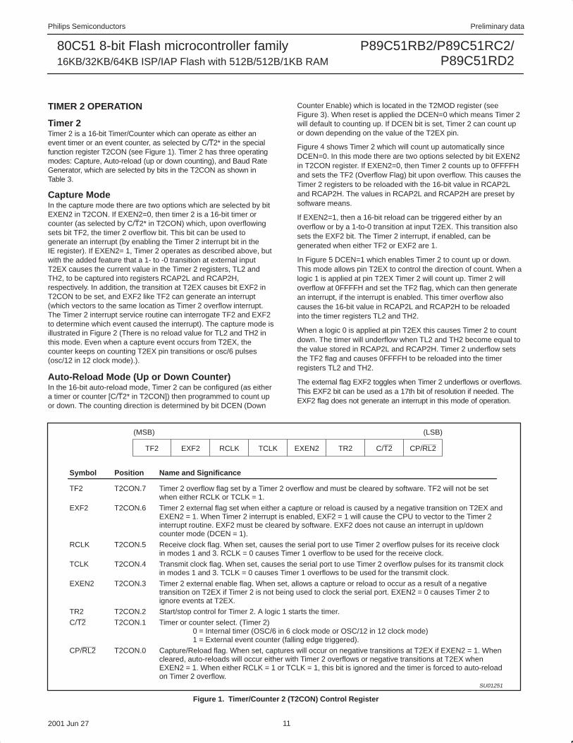
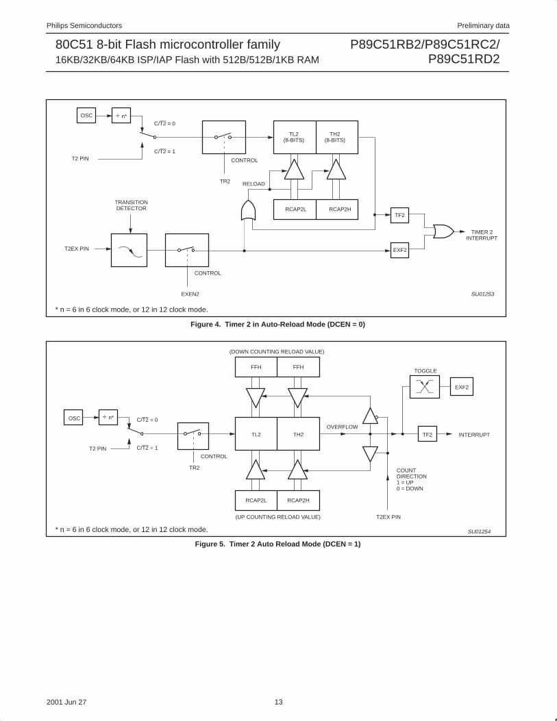
TIMER 2 OPERATION
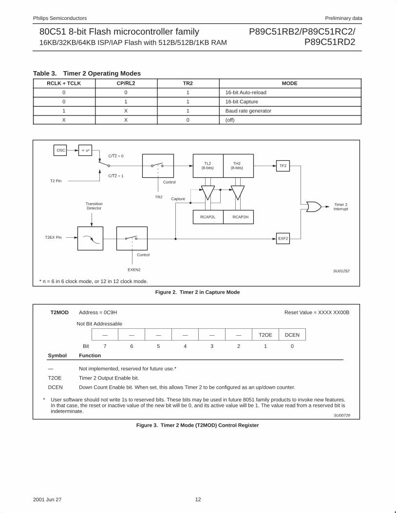
Timer 2Timer 2 is a 16-bit Timer/Counter which can operate as either anevent timer or an event counter, as selected by C/T2* in the specialfunction register T2CON (see Figure 1). Timer 2 has three operatingmodes: Capture, Auto-reload (up or down counting), and Baud RateGenerator, which are selected by bits in the T2CON as shown inTable 3.
Capture ModeIn the capture mode there are two options which are selected by bitEXEN2 in T2CON. If EXEN2=0, then timer 2 is a 16-bit timer orcounter (as selected by C/T2* in T2CON) which, upon overflowingsets bit TF2, the timer 2 overflow bit. This bit can be used togenerate an interrupt (by enabling the Timer 2 interrupt bit in theIE register). If EXEN2= 1, Timer 2 operates as described above, butwith the added feature that a 1- to -0 transition at external inputT2EX causes the current value in the Timer 2 registers, TL2 andTH2, to be captured into registers RCAP2L and RCAP2H,respectively. In addition, the transition at T2EX causes bit EXF2 inT2CON to be set, and EXF2 like TF2 can generate an interrupt(which vectors to the same location as Timer 2 overflow interrupt.The Timer 2 interrupt service routine can interrogate TF2 and EXF2to determine which event caused the interrupt). The capture mode isillustrated in Figure 2 (There is no reload value for TL2 and TH2 inthis mode. Even when a capture event occurs from T2EX, thecounter keeps on counting T2EX pin transitions or osc/6 pulses(osc/12 in 12 clock mode).).
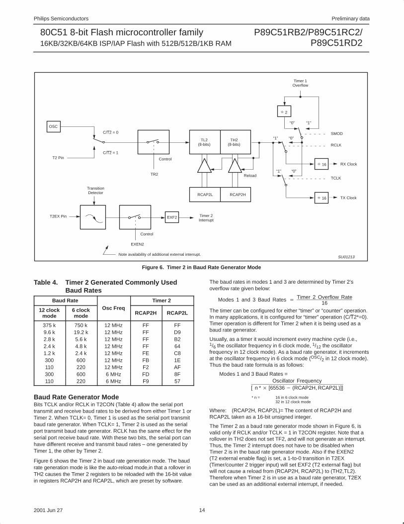
Auto-Reload Mode (Up or Down Counter)In the 16-bit auto-reload mode, Timer 2 can be configured (as eithera timer or counter [C/T2* in T2CON]) then programmed to count upor down. The counting direction is determined by bit DCEN (Down
Counter Enable) which is located in the T2MOD register (seeFigure 3). When reset is applied the DCEN=0 which means Timer 2will default to counting up. If DCEN bit is set, Timer 2 can count upor down depending on the value of the T2EX pin.
Figure 4 shows Timer 2 which will count up automatically sinceDCEN=0. In this mode there are two options selected by bit EXEN2in T2CON register. If EXEN2=0, then Timer 2 counts up to 0FFFFHand sets the TF2 (Overflow Flag) bit upon overflow. This causes theTimer 2 registers to be reloaded with the 16-bit value in RCAP2Land RCAP2H. The values in RCAP2L and RCAP2H are preset bysoftware means.
If EXEN2=1, then a 16-bit reload can be triggered either by anoverflow or by a 1-to-0 transition at input T2EX. This transition alsosets the EXF2 bit. The Timer 2 interrupt, if enabled, can begenerated when either TF2 or EXF2 are 1.
In Figure 5 DCEN=1 which enables Timer 2 to count up or down.This mode allows pin T2EX to control the direction of count. When alogic 1 is applied at pin T2EX Timer 2 will count up. Timer 2 willoverflow at 0FFFFH and set the TF2 flag, which can then generatean interrupt, if the interrupt is enabled. This timer overflow alsocauses the 16-bit value in RCAP2L and RCAP2H to be reloadedinto the timer registers TL2 and TH2.
When a logic 0 is applied at pin T2EX this causes Timer 2 to countdown. The timer will underflow when TL2 and TH2 become equal tothe value stored in RCAP2L and RCAP2H. Timer 2 underflow setsthe TF2 flag and causes 0FFFFH to be reloaded into the timerregisters TL2 and TH2.
The external flag EXF2 toggles when Timer 2 underflows or overflows.This EXF2 bit can be used as a 17th bit of resolution if needed. TheEXF2 flag does not generate an interrupt in this mode of operation.
(MSB) (LSB)
Symbol Position Name and Significance
TF2 T2CON.7 Timer 2 overflow flag set by a Timer 2 overflow and must be cleared by software. TF2 will not be setwhen either RCLK or TCLK = 1.
EXF2 T2CON.6 Timer 2 external flag set when either a capture or reload is caused by a negative transition on T2EX andEXEN2 = 1. When Timer 2 interrupt is enabled, EXF2 = 1 will cause the CPU to vector to the Timer 2interrupt routine. EXF2 must be cleared by software. EXF2 does not cause an interrupt in up/downcounter mode (DCEN = 1).
RCLK T2CON.5 Receive clock flag. When set, causes the serial port to use Timer 2 overflow pulses for its receive clockin modes 1 and 3. RCLK = 0 causes Timer 1 overflow to be used for the receive clock.
TCLK T2CON.4 Transmit clock flag. When set, causes the serial port to use Timer 2 overflow pulses for its transmit clockin modes 1 and 3. TCLK = 0 causes Timer 1 overflows to be used for the transmit clock.
EXEN2 T2CON.3 Timer 2 external enable flag. When set, allows a capture or reload to occur as a result of a negativetransition on T2EX if Timer 2 is not being used to clock the serial port. EXEN2 = 0 causes Timer 2 toignore events at T2EX.
TR2 T2CON.2 Start/stop control for Timer 2. A logic 1 starts the timer.
C/T2 T2CON.1 Timer or counter select. (Timer 2)0 = Internal timer (OSC/6 in 6 clock mode or OSC/12 in 12 clock mode)1 = External event counter (falling edge triggered).
CP/RL2 T2CON.0 Capture/Reload flag. When set, captures will occur on negative transitions at T2EX if EXEN2 = 1. Whencleared, auto-reloads will occur either with Timer 2 overflows or negative transitions at T2EX whenEXEN2 = 1. When either RCLK = 1 or TCLK = 1, this bit is ignored and the timer is forced to auto-reloadon Timer 2 overflow.
TF2 EXF2 RCLK TCLK EXEN2 TR2 C/T2 CP/RL2
SU01251
Figure 1. Timer/Counter 2 (T2CON) Control Register
Philips Semiconductors Preliminary data
P89C51RB2/P89C51RC2/P89C51RD2
80C51 8-bit Flash microcontroller family16KB/32KB/64KB ISP/IAP Flash with 512B/512B/1KB RAM
2001 Jun 27 12
Table 3. Timer 2 Operating ModesRCLK + TCLK CP/RL2 TR2 MODE
0 0 1 16-bit Auto-reload
0 1 1 16-bit Capture
1 X 1 Baud rate generator
X X 0 (off)
OSC ÷ n*C/T2 = 0
C/T2 = 1
TR2
Control
TL2(8-bits)
TH2(8-bits) TF2
RCAP2L RCAP2H
EXEN2
Control
EXF2
Timer 2Interrupt
T2EX Pin
TransitionDetector
T2 Pin
Capture
SU01252
* n = 6 in 6 clock mode, or 12 in 12 clock mode.
Figure 2. Timer 2 in Capture Mode
Not Bit Addressable
Symbol Function
— Not implemented, reserved for future use.*
T2OE Timer 2 Output Enable bit.
DCEN Down Count Enable bit. When set, this allows Timer 2 to be configured as an up/down counter.
— — — — — — T2OE DCEN
SU00729
7 6 5 4 3 2 1 0
* User software should not write 1s to reserved bits. These bits may be used in future 8051 family products to invoke new features.In that case, the reset or inactive value of the new bit will be 0, and its active value will be 1. The value read from a reserved bit isindeterminate.
Bit
T2MOD Address = 0C9H Reset Value = XXXX XX00B
Figure 3. Timer 2 Mode (T2MOD) Control Register
Philips Semiconductors Preliminary data
P89C51RB2/P89C51RC2/P89C51RD2
80C51 8-bit Flash microcontroller family16KB/32KB/64KB ISP/IAP Flash with 512B/512B/1KB RAM
2001 Jun 27 13
OSC ÷ n*C/T2 = 0
C/T2 = 1
TR2
CONTROL
TL2(8-BITS)
TH2(8-BITS)
TF2RCAP2L RCAP2H
EXEN2
CONTROL
EXF2
TIMER 2INTERRUPT
T2EX PIN
TRANSITIONDETECTOR
T2 PIN
RELOAD
SU01253
* n = 6 in 6 clock mode, or 12 in 12 clock mode.
Figure 4. Timer 2 in Auto-Reload Mode (DCEN = 0)
÷ n* C/T2 = 0
C/T2 = 1
TL2 TH2
TR2
CONTROLT2 PIN
SU01254
FFH FFH
RCAP2L RCAP2H
(UP COUNTING RELOAD VALUE) T2EX PIN
TF2 INTERRUPT
COUNTDIRECTION1 = UP0 = DOWN
EXF2
OVERFLOW
(DOWN COUNTING RELOAD VALUE)
TOGGLE
OSC
* n = 6 in 6 clock mode, or 12 in 12 clock mode.
Figure 5. Timer 2 Auto Reload Mode (DCEN = 1)
Philips Semiconductors Preliminary data
P89C51RB2/P89C51RC2/P89C51RD2
80C51 8-bit Flash microcontroller family16KB/32KB/64KB ISP/IAP Flash with 512B/512B/1KB RAM
2001 Jun 27 14
OSC
C/T2 = 0
C/T2 = 1
TR2
Control
TL2(8-bits)
TH2(8-bits)
÷ 16
RCAP2L RCAP2H
EXEN2
Control
EXF2 Timer 2Interrupt
T2EX Pin
TransitionDetector
T2 Pin
Reload
÷ 2
“0” “1”
RX Clock
÷ 16 TX Clock
“0”“1”
“0”“1”
Timer 1Overflow
Note availability of additional external interrupt.
SMOD
RCLK
TCLK
SU01213
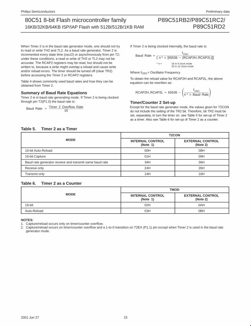
Figure 6. Timer 2 in Baud Rate Generator Mode
Table 4. Timer 2 Generated Commonly UsedBaud Rates
Baud Rate Timer 2
12 clockmode
6 clockmode
Osc FreqRCAP2H RCAP2L
375 k 750 k 12 MHz FF FF9.6 k 19.2 k 12 MHz FF D92.8 k 5.6 k 12 MHz FF B22.4 k 4.8 k 12 MHz FF 641.2 k 2.4 k 12 MHz FE C8300 600 12 MHz FB 1E110 220 12 MHz F2 AF300 600 6 MHz FD 8F110 220 6 MHz F9 57
Baud Rate Generator ModeBits TCLK and/or RCLK in T2CON (Table 4) allow the serial porttransmit and receive baud rates to be derived from either Timer 1 orTimer 2. When TCLK= 0, Timer 1 is used as the serial port transmitbaud rate generator. When TCLK= 1, Timer 2 is used as the serialport transmit baud rate generator. RCLK has the same effect for theserial port receive baud rate. With these two bits, the serial port canhave different receive and transmit baud rates – one generated byTimer 1, the other by Timer 2.
Figure 6 shows the Timer 2 in baud rate generation mode. The baudrate generation mode is like the auto-reload mode,in that a rollover inTH2 causes the Timer 2 registers to be reloaded with the 16-bit valuein registers RCAP2H and RCAP2L, which are preset by software.
The baud rates in modes 1 and 3 are determined by Timer 2’soverflow rate given below:
Modes 1 and 3 Baud Rates �Timer 2 Overflow Rate
16
The timer can be configured for either “timer” or “counter” operation.In many applications, it is configured for “timer” operation (C/T2*=0).Timer operation is different for Timer 2 when it is being used as abaud rate generator.
Usually, as a timer it would increment every machine cycle (i.e.,1/6 the oscillator frequency in 6 clock mode, 1/12 the oscillatorfrequency in 12 clock mode). As a baud rate generator, it incrementsat the oscillator frequency in 6 clock mode (OSC/2 in 12 clock mode).Thus the baud rate formula is as follows:
Oscillator Frequency[ n * � [65536 � (RCAP2H, RCAP2L)]]
Modes 1 and 3 Baud Rates =
* n = 16 in 6 clock mode32 in 12 clock mode
Where: (RCAP2H, RCAP2L)= The content of RCAP2H andRCAP2L taken as a 16-bit unsigned integer.
The Timer 2 as a baud rate generator mode shown in Figure 6, isvalid only if RCLK and/or TCLK = 1 in T2CON register. Note that arollover in TH2 does not set TF2, and will not generate an interrupt.Thus, the Timer 2 interrupt does not have to be disabled whenTimer 2 is in the baud rate generator mode. Also if the EXEN2(T2 external enable flag) is set, a 1-to-0 transition in T2EX(Timer/counter 2 trigger input) will set EXF2 (T2 external flag) butwill not cause a reload from (RCAP2H, RCAP2L) to (TH2,TL2).Therefore when Timer 2 is in use as a baud rate generator, T2EXcan be used as an additional external interrupt, if needed.
Philips Semiconductors Preliminary data
P89C51RB2/P89C51RC2/P89C51RD2
80C51 8-bit Flash microcontroller family16KB/32KB/64KB ISP/IAP Flash with 512B/512B/1KB RAM
2001 Jun 27 15
When Timer 2 is in the baud rate generator mode, one should not tryto read or write TH2 and TL2. As a baud rate generator, Timer 2 isincremented every state time (osc/2) or asynchronously from pin T2;under these conditions, a read or write of TH2 or TL2 may not beaccurate. The RCAP2 registers may be read, but should not bewritten to, because a write might overlap a reload and cause writeand/or reload errors. The timer should be turned off (clear TR2)before accessing the Timer 2 or RCAP2 registers.
Table 4 shows commonly used baud rates and how they can beobtained from Timer 2.
Summary of Baud Rate EquationsTimer 2 is in baud rate generating mode. If Timer 2 is being clockedthrough pin T2(P1.0) the baud rate is:
Baud Rate �Timer 2 Overflow Rate
16
If Timer 2 is being clocked internally, the baud rate is:
Baud Rate �
fOSC
[ n * � [65536 � (RCAP2H, RCAP2L)]]
* n = 16 in 6 clock mode32 in 12 clock mode
Where fOSC= Oscillator Frequency
To obtain the reload value for RCAP2H and RCAP2L, the aboveequation can be rewritten as:
RCAP2H, RCAP2L � 65536 ��fOSC
n * � Baud Rate�
Timer/Counter 2 Set-upExcept for the baud rate generator mode, the values given for T2CONdo not include the setting of the TR2 bit. Therefore, bit TR2 must beset, separately, to turn the timer on. see Table 5 for set-up of Timer 2as a timer. Also see Table 6 for set-up of Timer 2 as a counter.
Table 5. Timer 2 as a TimerT2CON
MODE INTERNAL CONTROL(Note 1)
EXTERNAL CONTROL(Note 2)
16-bit Auto-Reload 00H 08H
16-bit Capture 01H 09H
Baud rate generator receive and transmit same baud rate 34H 36H
Receive only 24H 26H
Transmit only 14H 16H
Table 6. Timer 2 as a CounterTMOD
MODE INTERNAL CONTROL(Note 1)
EXTERNAL CONTROL(Note 2)
16-bit 02H 0AH
Auto-Reload 03H 0BH
NOTES:1. Capture/reload occurs only on timer/counter overflow.2. Capture/reload occurs on timer/counter overflow and a 1-to-0 transition on T2EX (P1.1) pin except when Timer 2 is used in the baud rate
generator mode.
Philips Semiconductors Preliminary data
P89C51RB2/P89C51RC2/P89C51RD2
80C51 8-bit Flash microcontroller family16KB/32KB/64KB ISP/IAP Flash with 512B/512B/1KB RAM
2001 Jun 27 16
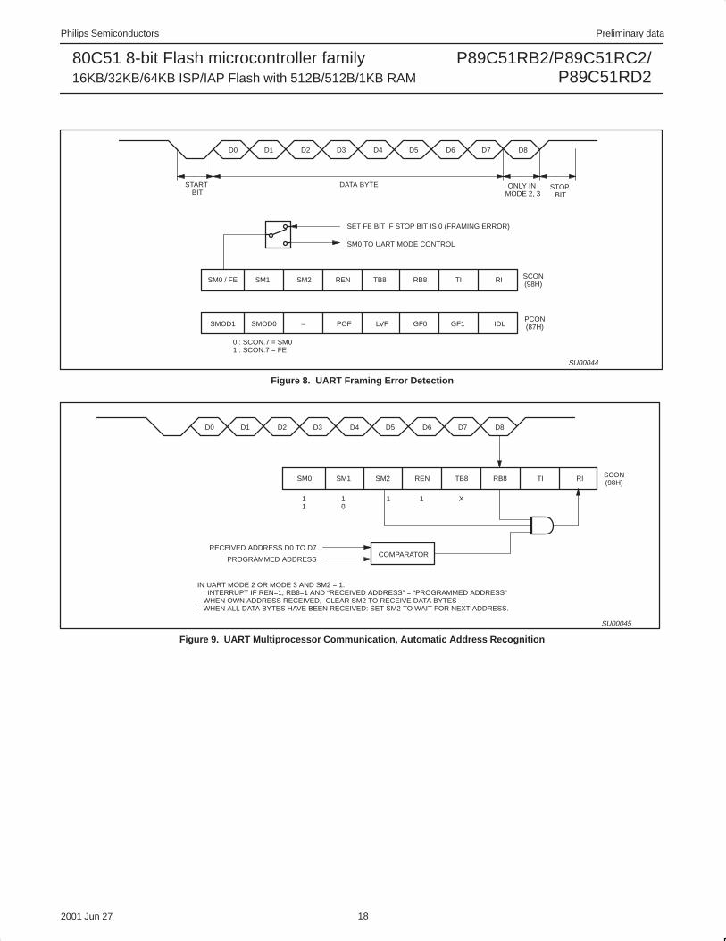
Enhanced UARTThe UART operates in all of the usual modes that are described inthe first section of Data Handbook IC20, 80C51-Based 8-BitMicrocontrollers. In addition the UART can perform framing errordetect by looking for missing stop bits, and automatic addressrecognition. The UART also fully supports multiprocessorcommunication as does the standard 80C51 UART.
When used for framing error detect the UART looks for missing stopbits in the communication. A missing bit will set the FE bit in theSCON register. The FE bit shares the SCON.7 bit with SM0 and thefunction of SCON.7 is determined by PCON.6 (SMOD0) (seeFigure 7). If SMOD0 is set then SCON.7 functions as FE. SCON.7functions as SM0 when SMOD0 is cleared. When used as FESCON.7 can only be cleared by software. Refer to Figure 8.
Automatic Address RecognitionAutomatic Address Recognition is a feature which allows the UARTto recognize certain addresses in the serial bit stream by usinghardware to make the comparisons. This feature saves a great dealof software overhead by eliminating the need for the software toexamine every serial address which passes by the serial port. Thisfeature is enabled by setting the SM2 bit in SCON. In the 9 bit UARTmodes, mode 2 and mode 3, the Receive Interrupt flag (RI) will beautomatically set when the received byte contains either the “Given”address or the “Broadcast” address. The 9-bit mode requires thatthe 9th information bit is a 1 to indicate that the received informationis an address and not data. Automatic address recognition is shownin Figure 9.
The 8 bit mode is called Mode 1. In this mode the RI flag will be setif SM2 is enabled and the information received has a valid stop bitfollowing the 8 address bits and the information is either a Given orBroadcast address.
Mode 0 is the Shift Register mode and SM2 is ignored.
Using the Automatic Address Recognition feature allows a master toselectively communicate with one or more slaves by invoking theGiven slave address or addresses. All of the slaves may becontacted by using the Broadcast address. Two special FunctionRegisters are used to define the slave’s address, SADDR, and theaddress mask, SADEN. SADEN is used to define which bits in theSADDR are to b used and which bits are “don’t care”. The SADENmask can be logically ANDed with the SADDR to create the “Given”address which the master will use for addressing each of the slaves.Use of the Given address allows multiple slaves to be recognizedwhile excluding others. The following examples will help to show theversatility of this scheme:
Slave 0 SADDR = 1100 0000SADEN = 1111 1101Given = 1100 00X0
Slave 1 SADDR = 1100 0000SADEN = 1111 1110Given = 1100 000X
In the above example SADDR is the same and the SADEN data isused to differentiate between the two slaves. Slave 0 requires a 0 inbit 0 and it ignores bit 1. Slave 1 requires a 0 in bit 1 and bit 0 isignored. A unique address for Slave 0 would be 1100 0010 sinceslave 1 requires a 0 in bit 1. A unique address for slave 1 would be1100 0001 since a 1 in bit 0 will exclude slave 0. Both slaves can beselected at the same time by an address which has bit 0 = 0 (forslave 0) and bit 1 = 0 (for slave 1). Thus, both could be addressedwith 1100 0000.
In a more complex system the following could be used to selectslaves 1 and 2 while excluding slave 0:
Slave 0 SADDR = 1100 0000SADEN = 1111 1001Given = 1100 0XX0
Slave 1 SADDR = 1110 0000SADEN = 1111 1010Given = 1110 0X0X
Slave 2 SADDR = 1110 0000SADEN = 1111 1100Given = 1110 00XX
In the above example the differentiation among the 3 slaves is in thelower 3 address bits. Slave 0 requires that bit 0 = 0 and it can beuniquely addressed by 1110 0110. Slave 1 requires that bit 1 = 0 andit can be uniquely addressed by 1110 and 0101. Slave 2 requiresthat bit 2 = 0 and its unique address is 1110 0011. To select Slaves 0and 1 and exclude Slave 2 use address 1110 0100, since it isnecessary to make bit 2 = 1 to exclude slave 2.
The Broadcast Address for each slave is created by taking thelogical OR of SADDR and SADEN. Zeros in this result are trendedas don’t-cares. In most cases, interpreting the don’t-cares as ones,the broadcast address will be FF hexadecimal.
Upon reset SADDR (SFR address 0A9H) and SADEN (SFRaddress 0B9H) are leaded with 0s. This produces a given addressof all “don’t cares” as well as a Broadcast address of all “don’tcares”. This effectively disables the Automatic Addressing mode andallows the microcontroller to use standard 80C51 type UART driverswhich do not make use of this feature.
Philips Semiconductors Preliminary data
P89C51RB2/P89C51RC2/P89C51RD2
80C51 8-bit Flash microcontroller family16KB/32KB/64KB ISP/IAP Flash with 512B/512B/1KB RAM
2001 Jun 27 17
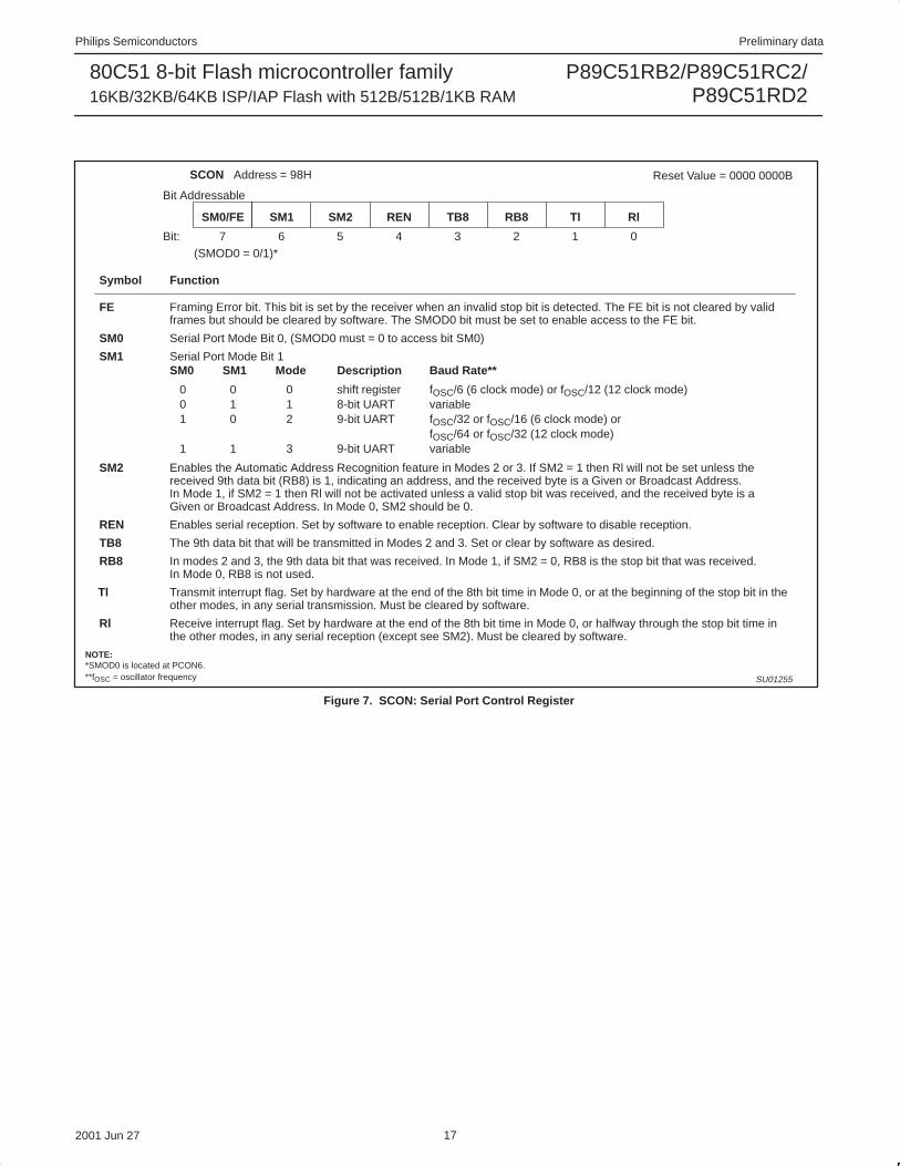
SCON Address = 98H Reset Value = 0000 0000B
SM0/FE SM1 SM2 REN TB8 RB8 Tl Rl
Bit Addressable
(SMOD0 = 0/1)*
Symbol Function
FE Framing Error bit. This bit is set by the receiver when an invalid stop bit is detected. The FE bit is not cleared by validframes but should be cleared by software. The SMOD0 bit must be set to enable access to the FE bit.
SM0 Serial Port Mode Bit 0, (SMOD0 must = 0 to access bit SM0)
SM1 Serial Port Mode Bit 1SM0 SM1 Mode Description Baud Rate**
0 0 0 shift register fOSC/6 (6 clock mode) or fOSC/12 (12 clock mode)0 1 1 8-bit UART variable1 0 2 9-bit UART fOSC/32 or fOSC/16 (6 clock mode) or
fOSC/64 or fOSC/32 (12 clock mode)1 1 3 9-bit UART variable
SM2 Enables the Automatic Address Recognition feature in Modes 2 or 3. If SM2 = 1 then Rl will not be set unless thereceived 9th data bit (RB8) is 1, indicating an address, and the received byte is a Given or Broadcast Address.In Mode 1, if SM2 = 1 then Rl will not be activated unless a valid stop bit was received, and the received byte is aGiven or Broadcast Address. In Mode 0, SM2 should be 0.
REN Enables serial reception. Set by software to enable reception. Clear by software to disable reception.
TB8 The 9th data bit that will be transmitted in Modes 2 and 3. Set or clear by software as desired.
RB8 In modes 2 and 3, the 9th data bit that was received. In Mode 1, if SM2 = 0, RB8 is the stop bit that was received. In Mode 0, RB8 is not used.
Tl Transmit interrupt flag. Set by hardware at the end of the 8th bit time in Mode 0, or at the beginning of the stop bit in theother modes, in any serial transmission. Must be cleared by software.
Rl Receive interrupt flag. Set by hardware at the end of the 8th bit time in Mode 0, or halfway through the stop bit time inthe other modes, in any serial reception (except see SM2). Must be cleared by software.
NOTE:*SMOD0 is located at PCON6.**fOSC = oscillator frequency SU01255
Bit: 7 6 5 4 3 2 1 0
Figure 7. SCON: Serial Port Control Register
Philips Semiconductors Preliminary data
P89C51RB2/P89C51RC2/P89C51RD2
80C51 8-bit Flash microcontroller family16KB/32KB/64KB ISP/IAP Flash with 512B/512B/1KB RAM
2001 Jun 27 18
SMOD1 SMOD0 – POF LVF GF0 GF1 IDLPCON(87H)
SM0 / FE SM1 SM2 REN TB8 RB8 TI RI SCON(98H)
D0 D1 D2 D3 D4 D5 D6 D7 D8
STOP BIT
DATA BYTE ONLY IN MODE 2, 3
START BIT
SET FE BIT IF STOP BIT IS 0 (FRAMING ERROR)
SM0 TO UART MODE CONTROL
0 : SCON.7 = SM01 : SCON.7 = FE
SU00044
Figure 8. UART Framing Error Detection
SM0 SM1 SM2 REN TB8 RB8 TI RI SCON(98H)
D0 D1 D2 D3 D4 D5 D6 D7 D8
11
10
COMPARATOR
1 1 X
RECEIVED ADDRESS D0 TO D7
PROGRAMMED ADDRESS
IN UART MODE 2 OR MODE 3 AND SM2 = 1: INTERRUPT IF REN=1, RB8=1 AND “RECEIVED ADDRESS” = “PROGRAMMED ADDRESS”– WHEN OWN ADDRESS RECEIVED, CLEAR SM2 TO RECEIVE DATA BYTES– WHEN ALL DATA BYTES HAVE BEEN RECEIVED: SET SM2 TO WAIT FOR NEXT ADDRESS.
SU00045
Figure 9. UART Multiprocessor Communication, Automatic Address Recognition
Philips Semiconductors Preliminary data
P89C51RB2/P89C51RC2/P89C51RD2
80C51 8-bit Flash microcontroller family16KB/32KB/64KB ISP/IAP Flash with 512B/512B/1KB RAM
2001 Jun 27 19
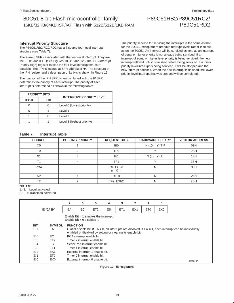
Interrupt Priority StructureThe P89C51RB2/RC2/RD2 has a 7 source four-level interruptstructure (see Table 7).
There are 3 SFRs associated with the four-level interrupt. They arethe IE, IP, and IPH. (See Figures 10, 11, and 12.) The IPH (InterruptPriority High) register makes the four-level interrupt structurepossible. The IPH is located at SFR address B7H. The structure ofthe IPH register and a description of its bits is shown in Figure 12.
The function of the IPH SFR, when combined with the IP SFR,determines the priority of each interrupt. The priority of eachinterrupt is determined as shown in the following table:
PRIORITY BITSINTERRUPT PRIORITY LEVEL
IPH.x IP.xINTERRUPT PRIORITY LEVEL
0 0 Level 0 (lowest priority)
0 1 Level 1
1 0 Level 2
1 1 Level 3 (highest priority)
The priority scheme for servicing the interrupts is the same as thatfor the 80C51, except there are four interrupt levels rather than twoas on the 80C51. An interrupt will be serviced as long as an interruptof equal or higher priority is not already being serviced. If aninterrupt of equal or higher level priority is being serviced, the newinterrupt will wait until it is finished before being serviced. If a lowerpriority level interrupt is being serviced, it will be stopped and thenew interrupt serviced. When the new interrupt is finished, the lowerpriority level interrupt that was stopped will be completed.
Table 7. Interrupt TableSOURCE POLLING PRIORITY REQUEST BITS HARDWARE CLEAR? VECTOR ADDRESS
X0 1 IE0 N (L)1 Y (T)2 03H
T0 2 TP0 Y 0BH
X1 3 IE1 N (L) Y (T) 13H
T1 4 TF1 Y 1BH
PCA 5 CF, CCFnn = 0–4
N 33H
SP 6 RI, TI N 23H
T2 7 TF2, EXF2 N 2BH
NOTES:1. L = Level activated2. T = Transition activated
EX0IE (0A8H)
Enable Bit = 1 enables the interrupt.Enable Bit = 0 disables it.
BIT SYMBOL FUNCTIONIE.7 EA Global disable bit. If EA = 0, all interrupts are disabled. If EA = 1, each interrupt can be individually
enabled or disabled by setting or clearing its enable bit.IE.6 EC PCA interrupt enable bitIE.5 ET2 Timer 2 interrupt enable bit.IE.4 ES Serial Port interrupt enable bit.IE.3 ET1 Timer 1 interrupt enable bit.IE.2 EX1 External interrupt 1 enable bit.IE.1 ET0 Timer 0 interrupt enable bit.IE.0 EX0 External interrupt 0 enable bit.
SU01290
ET0EX1ET1ESET2ECEA
01234567
Figure 10. IE Registers
Philips Semiconductors Preliminary data
P89C51RB2/P89C51RC2/P89C51RD2
80C51 8-bit Flash microcontroller family16KB/32KB/64KB ISP/IAP Flash with 512B/512B/1KB RAM
2001 Jun 27 20
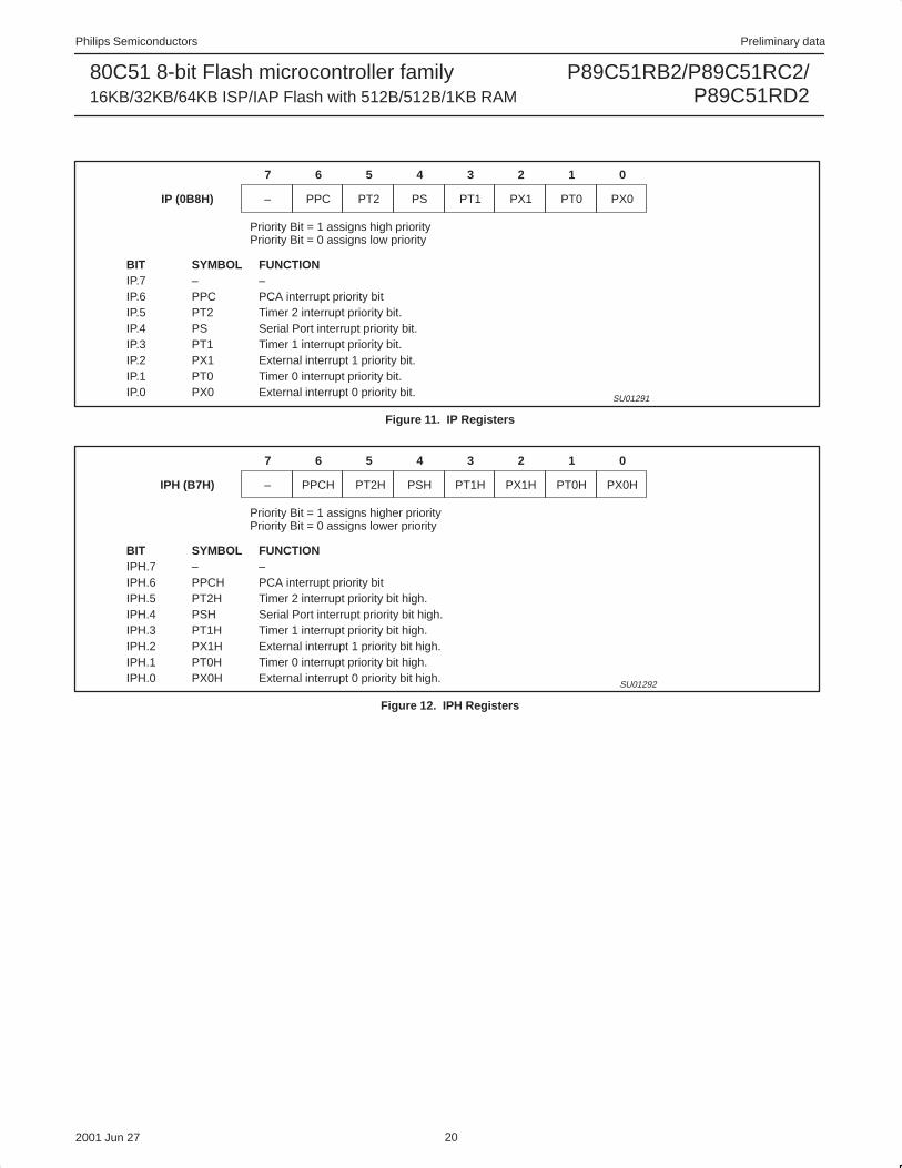
PX0IP (0B8H)
Priority Bit = 1 assigns high priorityPriority Bit = 0 assigns low priority
BIT SYMBOL FUNCTIONIP.7 – –IP.6 PPC PCA interrupt priority bitIP.5 PT2 Timer 2 interrupt priority bit.IP.4 PS Serial Port interrupt priority bit.IP.3 PT1 Timer 1 interrupt priority bit.IP.2 PX1 External interrupt 1 priority bit.IP.1 PT0 Timer 0 interrupt priority bit.IP.0 PX0 External interrupt 0 priority bit.
SU01291
PT0PX1PT1PSPT2PPC–
01234567
Figure 11. IP Registers
PX0HIPH (B7H)
Priority Bit = 1 assigns higher priorityPriority Bit = 0 assigns lower priority
BIT SYMBOL FUNCTIONIPH.7 – –IPH.6 PPCH PCA interrupt priority bitIPH.5 PT2H Timer 2 interrupt priority bit high.IPH.4 PSH Serial Port interrupt priority bit high.IPH.3 PT1H Timer 1 interrupt priority bit high.IPH.2 PX1H External interrupt 1 priority bit high.IPH.1 PT0H Timer 0 interrupt priority bit high.IPH.0 PX0H External interrupt 0 priority bit high.
SU01292
PT0HPX1HPT1HPSHPT2HPPCH–
01234567
Figure 12. IPH Registers
Philips Semiconductors Preliminary data
P89C51RB2/P89C51RC2/P89C51RD2
80C51 8-bit Flash microcontroller family16KB/32KB/64KB ISP/IAP Flash with 512B/512B/1KB RAM
2001 Jun 27 21
Reduced EMI ModeThe AO bit (AUXR.0) in the AUXR register when set disables theALE output.
Reduced EMI Mode
AUXR (8EH)
7 6 5 4 3 2 1 0
– – – – – – EXTRAM AO
AUXR.1 EXTRAMAUXR.0 AO Turns off ALE output.
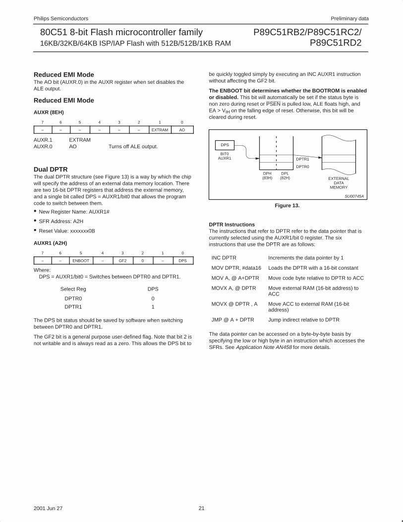
Dual DPTRThe dual DPTR structure (see Figure 13) is a way by which the chipwill specify the address of an external data memory location. Thereare two 16-bit DPTR registers that address the external memory,and a single bit called DPS = AUXR1/bit0 that allows the programcode to switch between them.
• New Register Name: AUXR1#
• SFR Address: A2H
• Reset Value: xxxxxxx0B
AUXR1 (A2H)
7 6 5 4 3 2 1 0
– – ENBOOT – GF2 0 – DPS
Where:DPS = AUXR1/bit0 = Switches between DPTR0 and DPTR1.
Select Reg DPS
DPTR0 0
DPTR1 1
The DPS bit status should be saved by software when switchingbetween DPTR0 and DPTR1.
The GF2 bit is a general purpose user-defined flag. Note that bit 2 isnot writable and is always read as a zero. This allows the DPS bit to
be quickly toggled simply by executing an INC AUXR1 instructionwithout affecting the GF2 bit.
The ENBOOT bit determines whether the BOOTROM is enabledor disabled. This bit will automatically be set if the status byte isnon zero during reset or PSEN is pulled low, ALE floats high, andEA > VIH on the falling edge of reset. Otherwise, this bit will becleared during reset.
DPS
DPTR1
DPTR0
DPH(83H)
DPL(82H) EXTERNAL
DATAMEMORY
SU00745A
BIT0AUXR1
Figure 13.
DPTR InstructionsThe instructions that refer to DPTR refer to the data pointer that iscurrently selected using the AUXR1/bit 0 register. The sixinstructions that use the DPTR are as follows:
INC DPTR Increments the data pointer by 1
MOV DPTR, #data16 Loads the DPTR with a 16-bit constant
MOV A, @ A+DPTR Move code byte relative to DPTR to ACC
MOVX A, @ DPTR Move external RAM (16-bit address) toACC
MOVX @ DPTR , A Move ACC to external RAM (16-bitaddress)
JMP @ A + DPTR Jump indirect relative to DPTR
The data pointer can be accessed on a byte-by-byte basis byspecifying the low or high byte in an instruction which accesses theSFRs. See Application Note AN458 for more details.
Philips Semiconductors Preliminary data
P89C51RB2/P89C51RC2/P89C51RD2
80C51 8-bit Flash microcontroller family16KB/32KB/64KB ISP/IAP Flash with 512B/512B/1KB RAM
2001 Jun 27 22
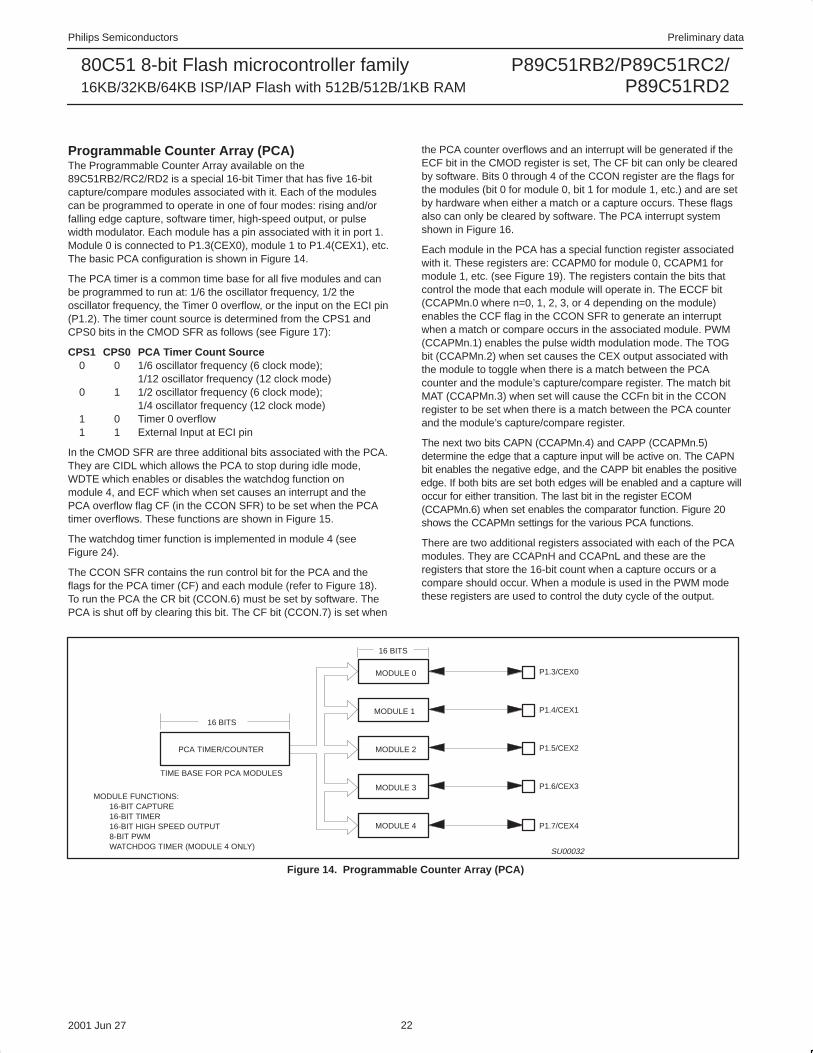
Programmable Counter Array (PCA)The Programmable Counter Array available on the89C51RB2/RC2/RD2 is a special 16-bit Timer that has five 16-bitcapture/compare modules associated with it. Each of the modulescan be programmed to operate in one of four modes: rising and/orfalling edge capture, software timer, high-speed output, or pulsewidth modulator. Each module has a pin associated with it in port 1.Module 0 is connected to P1.3(CEX0), module 1 to P1.4(CEX1), etc.The basic PCA configuration is shown in Figure 14.
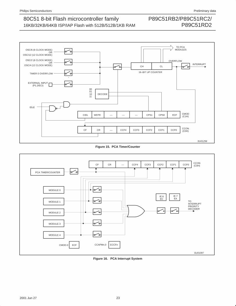
The PCA timer is a common time base for all five modules and canbe programmed to run at: 1/6 the oscillator frequency, 1/2 theoscillator frequency, the Timer 0 overflow, or the input on the ECI pin(P1.2). The timer count source is determined from the CPS1 andCPS0 bits in the CMOD SFR as follows (see Figure 17):
CPS1 CPS0 PCA Timer Count Source0 0 1/6 oscillator frequency (6 clock mode);
1/12 oscillator frequency (12 clock mode)0 1 1/2 oscillator frequency (6 clock mode);
1/4 oscillator frequency (12 clock mode)1 0 Timer 0 overflow1 1 External Input at ECI pin
In the CMOD SFR are three additional bits associated with the PCA.They are CIDL which allows the PCA to stop during idle mode,WDTE which enables or disables the watchdog function onmodule 4, and ECF which when set causes an interrupt and thePCA overflow flag CF (in the CCON SFR) to be set when the PCAtimer overflows. These functions are shown in Figure 15.
The watchdog timer function is implemented in module 4 (seeFigure 24).
The CCON SFR contains the run control bit for the PCA and theflags for the PCA timer (CF) and each module (refer to Figure 18).To run the PCA the CR bit (CCON.6) must be set by software. ThePCA is shut off by clearing this bit. The CF bit (CCON.7) is set when
the PCA counter overflows and an interrupt will be generated if theECF bit in the CMOD register is set, The CF bit can only be clearedby software. Bits 0 through 4 of the CCON register are the flags forthe modules (bit 0 for module 0, bit 1 for module 1, etc.) and are setby hardware when either a match or a capture occurs. These flagsalso can only be cleared by software. The PCA interrupt systemshown in Figure 16.
Each module in the PCA has a special function register associatedwith it. These registers are: CCAPM0 for module 0, CCAPM1 formodule 1, etc. (see Figure 19). The registers contain the bits thatcontrol the mode that each module will operate in. The ECCF bit(CCAPMn.0 where n=0, 1, 2, 3, or 4 depending on the module)enables the CCF flag in the CCON SFR to generate an interruptwhen a match or compare occurs in the associated module. PWM(CCAPMn.1) enables the pulse width modulation mode. The TOGbit (CCAPMn.2) when set causes the CEX output associated withthe module to toggle when there is a match between the PCAcounter and the module’s capture/compare register. The match bitMAT (CCAPMn.3) when set will cause the CCFn bit in the CCONregister to be set when there is a match between the PCA counterand the module’s capture/compare register.
The next two bits CAPN (CCAPMn.4) and CAPP (CCAPMn.5)determine the edge that a capture input will be active on. The CAPNbit enables the negative edge, and the CAPP bit enables the positiveedge. If both bits are set both edges will be enabled and a capture willoccur for either transition. The last bit in the register ECOM(CCAPMn.6) when set enables the comparator function. Figure 20shows the CCAPMn settings for the various PCA functions.
There are two additional registers associated with each of the PCAmodules. They are CCAPnH and CCAPnL and these are theregisters that store the 16-bit count when a capture occurs or acompare should occur. When a module is used in the PWM modethese registers are used to control the duty cycle of the output.
MODULE FUNCTIONS:16-BIT CAPTURE16-BIT TIMER16-BIT HIGH SPEED OUTPUT8-BIT PWMWATCHDOG TIMER (MODULE 4 ONLY)
MODULE 0
MODULE 1
MODULE 2
MODULE 3
MODULE 4
P1.3/CEX0
P1.4/CEX1
P1.5/CEX2
P1.6/CEX3
P1.7/CEX4
16 BITS
PCA TIMER/COUNTER
TIME BASE FOR PCA MODULES
16 BITS
SU00032
Figure 14. Programmable Counter Array (PCA)
Philips Semiconductors Preliminary data
P89C51RB2/P89C51RC2/P89C51RD2
80C51 8-bit Flash microcontroller family16KB/32KB/64KB ISP/IAP Flash with 512B/512B/1KB RAM
2001 Jun 27 23
CF CR CCF4 CCF3 CCF2 CCF1 CCF0––CCON(C0H)
CH CL
OVERFLOWINTERRUPT
16–BIT UP COUNTER
IDLE
TO PCA MODULES
CMOD(C1H)
CIDL WDTE –– –– –– CPS1 CPS0 ECF
OSC/6 (6 CLOCK MODE)OR
OSC/12 (12 CLOCK MODE)
TIMER 0 OVERFLOW
EXTERNAL INPUT(P1.2/ECI)
DECODE
00011011
SU01256
OSC/2 (6 CLOCK MODE)OR
OSC/4 (12 CLOCK MODE)
Figure 15. PCA Timer/Counter
MODULE 0
MODULE 1
MODULE 2
MODULE 3
MODULE 4
PCA TIMER/COUNTER
CF CR CCF4 CCF3 CCF2 CCF1 CCF0––
CMOD.0 ECF CCAPMn.0 ECCFn
TO INTERRUPT PRIORITY DECODER
CCON(C0H)
IE.6EC
IE.7EA
SU01097
Figure 16. PCA Interrupt System
Philips Semiconductors Preliminary data
P89C51RB2/P89C51RC2/P89C51RD2
80C51 8-bit Flash microcontroller family16KB/32KB/64KB ISP/IAP Flash with 512B/512B/1KB RAM
2001 Jun 27 24
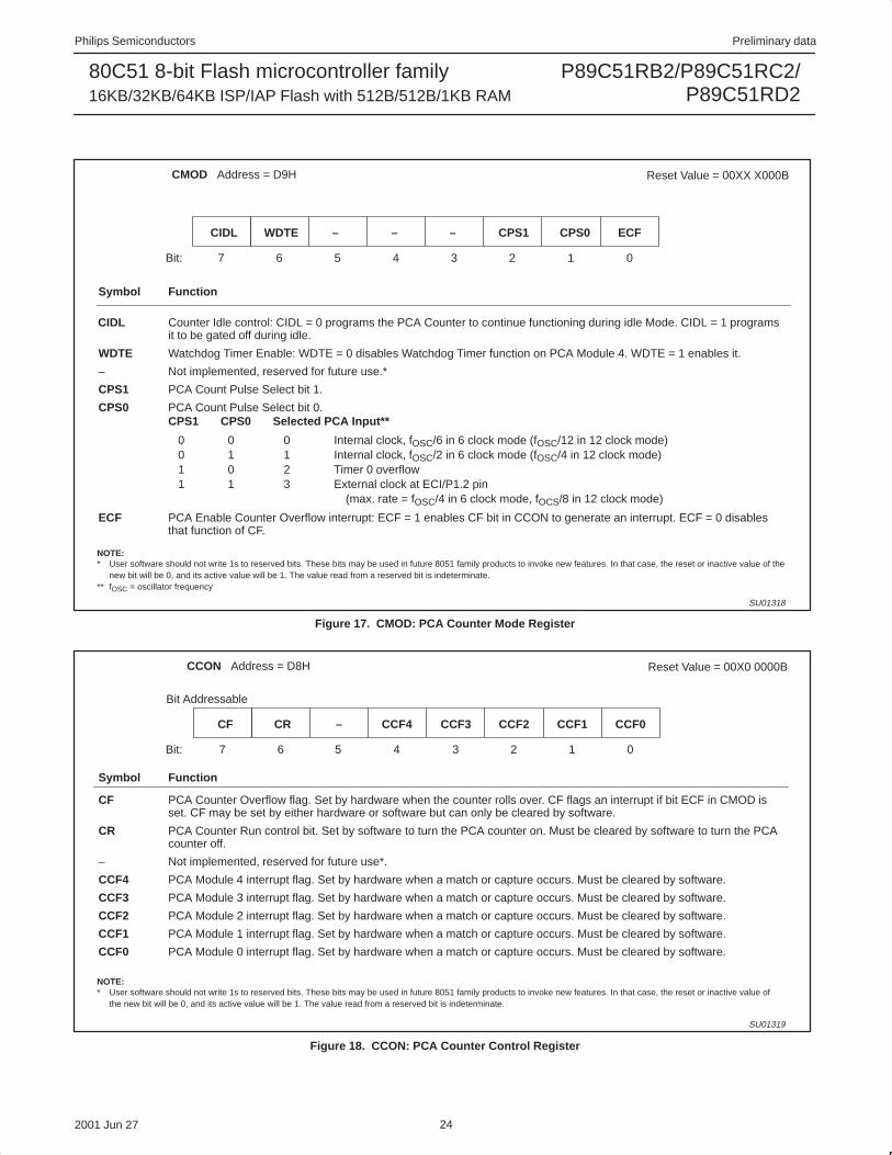
CMOD Address = D9H Reset Value = 00XX X000B
CIDL WDTE – – – CPS1 CPS0 ECF
Bit:
Symbol Function
CIDL Counter Idle control: CIDL = 0 programs the PCA Counter to continue functioning during idle Mode. CIDL = 1 programsit to be gated off during idle.
WDTE Watchdog Timer Enable: WDTE = 0 disables Watchdog Timer function on PCA Module 4. WDTE = 1 enables it.
– Not implemented, reserved for future use.*
CPS1 PCA Count Pulse Select bit 1.
CPS0 PCA Count Pulse Select bit 0.CPS1 CPS0 Selected PCA Input**
0 0 0 Internal clock, fOSC/6 in 6 clock mode (fOSC/12 in 12 clock mode)0 1 1 Internal clock, fOSC/2 in 6 clock mode (fOSC/4 in 12 clock mode)1 0 2 Timer 0 overflow1 1 3 External clock at ECI/P1.2 pin
(max. rate = fOSC/4 in 6 clock mode, fOCS/8 in 12 clock mode)
ECF PCA Enable Counter Overflow interrupt: ECF = 1 enables CF bit in CCON to generate an interrupt. ECF = 0 disablesthat function of CF.
NOTE:* User software should not write 1s to reserved bits. These bits may be used in future 8051 family products to invoke new features. In that case, the reset or inactive value of the
new bit will be 0, and its active value will be 1. The value read from a reserved bit is indeterminate.** fOSC = oscillator frequency
SU01318
7 6 5 4 3 2 1 0
Figure 17. CMOD: PCA Counter Mode Register
CCON Address = D8H Reset Value = 00X0 0000B
CF CR – CCF4 CCF3 CCF2 CCF1 CCF0
Bit Addressable
Bit:
Symbol Function
CF PCA Counter Overflow flag. Set by hardware when the counter rolls over. CF flags an interrupt if bit ECF in CMOD isset. CF may be set by either hardware or software but can only be cleared by software.
CR PCA Counter Run control bit. Set by software to turn the PCA counter on. Must be cleared by software to turn the PCAcounter off.
– Not implemented, reserved for future use*.
CCF4 PCA Module 4 interrupt flag. Set by hardware when a match or capture occurs. Must be cleared by software.
CCF3 PCA Module 3 interrupt flag. Set by hardware when a match or capture occurs. Must be cleared by software.
CCF2 PCA Module 2 interrupt flag. Set by hardware when a match or capture occurs. Must be cleared by software.
CCF1 PCA Module 1 interrupt flag. Set by hardware when a match or capture occurs. Must be cleared by software.
CCF0 PCA Module 0 interrupt flag. Set by hardware when a match or capture occurs. Must be cleared by software.
NOTE:* User software should not write 1s to reserved bits. These bits may be used in future 8051 family products to invoke new features. In that case, the reset or inactive value of
the new bit will be 0, and its active value will be 1. The value read from a reserved bit is indeterminate.
SU01319
7 6 5 4 3 2 1 0
Figure 18. CCON: PCA Counter Control Register
Philips Semiconductors Preliminary data
P89C51RB2/P89C51RC2/P89C51RD2
80C51 8-bit Flash microcontroller family16KB/32KB/64KB ISP/IAP Flash with 512B/512B/1KB RAM
2001 Jun 27 25
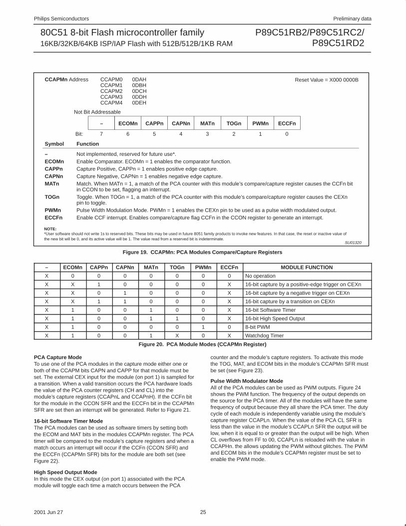
CCAPMn Address CCAPM0 0DAHCCAPM1 0DBHCCAPM2 0DCH CCAPM3 0DDH CCAPM4 0DEH
Reset Value = X000 0000B
– ECOMn CAPPn CAPNn MATn TOGn PWMn ECCFn
Not Bit Addressable
Bit:
Symbol Function
– Not implemented, reserved for future use*.ECOMn Enable Comparator. ECOMn = 1 enables the comparator function.CAPPn Capture Positive, CAPPn = 1 enables positive edge capture.CAPNn Capture Negative, CAPNn = 1 enables negative edge capture.MATn Match. When MATn = 1, a match of the PCA counter with this module’s compare/capture register causes the CCFn bit
in CCON to be set, flagging an interrupt.TOGn Toggle. When TOGn = 1, a match of the PCA counter with this module’s compare/capture register causes the CEXn
pin to toggle.PWMn Pulse Width Modulation Mode. PWMn = 1 enables the CEXn pin to be used as a pulse width modulated output.ECCFn Enable CCF interrupt. Enables compare/capture flag CCFn in the CCON register to generate an interrupt.
NOTE:*User software should not write 1s to reserved bits. These bits may be used in future 8051 family products to invoke new features. In that case, the reset or inactive value ofthe new bit will be 0, and its active value will be 1. The value read from a reserved bit is indeterminate.
SU01320
7 6 5 4 3 2 1 0
Figure 19. CCAPMn: PCA Modules Compare/Capture Registers
– ECOMn CAPPn CAPNn MATn TOGn PWMn ECCFn MODULE FUNCTION
X 0 0 0 0 0 0 0 No operation
X X 1 0 0 0 0 X 16-bit capture by a positive-edge trigger on CEXn
X X 0 1 0 0 0 X 16-bit capture by a negative trigger on CEXn
X X 1 1 0 0 0 X 16-bit capture by a transition on CEXn
X 1 0 0 1 0 0 X 16-bit Software Timer
X 1 0 0 1 1 0 X 16-bit High Speed Output
X 1 0 0 0 0 1 0 8-bit PWM
X 1 0 0 1 X 0 X Watchdog Timer
Figure 20. PCA Module Modes (CCAPMn Register)
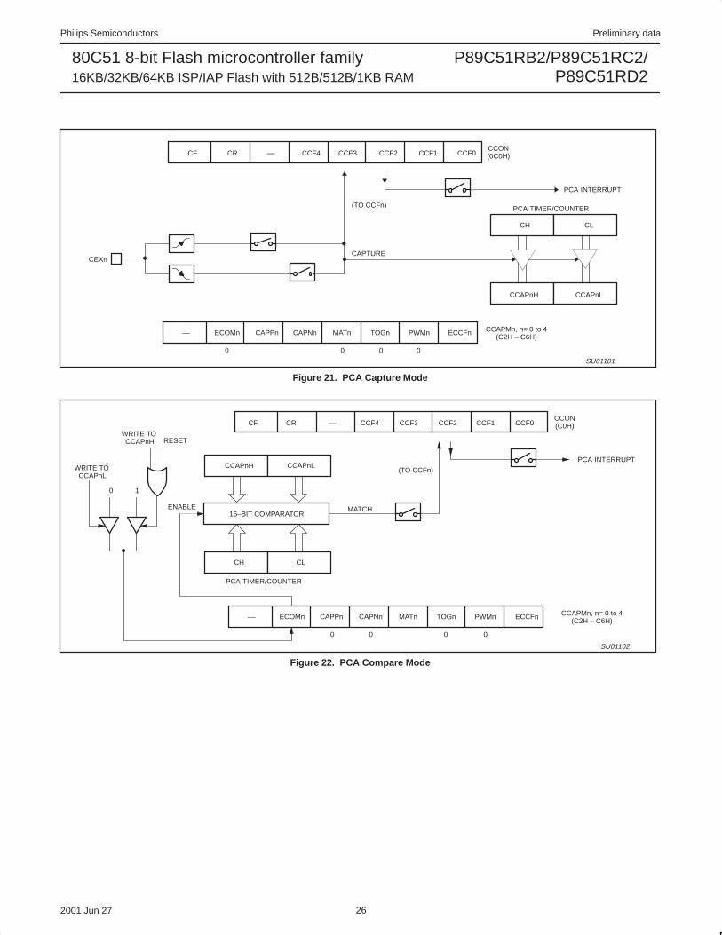
PCA Capture ModeTo use one of the PCA modules in the capture mode either one orboth of the CCAPM bits CAPN and CAPP for that module must beset. The external CEX input for the module (on port 1) is sampled fora transition. When a valid transition occurs the PCA hardware loadsthe value of the PCA counter registers (CH and CL) into themodule’s capture registers (CCAPnL and CCAPnH). If the CCFn bitfor the module in the CCON SFR and the ECCFn bit in the CCAPMnSFR are set then an interrupt will be generated. Refer to Figure 21.
16-bit Software Timer ModeThe PCA modules can be used as software timers by setting boththe ECOM and MAT bits in the modules CCAPMn register. The PCAtimer will be compared to the module’s capture registers and when amatch occurs an interrupt will occur if the CCFn (CCON SFR) andthe ECCFn (CCAPMn SFR) bits for the module are both set (seeFigure 22).
High Speed Output ModeIn this mode the CEX output (on port 1) associated with the PCAmodule will toggle each time a match occurs between the PCA
counter and the module’s capture registers. To activate this modethe TOG, MAT, and ECOM bits in the module’s CCAPMn SFR mustbe set (see Figure 23).
Pulse Width Modulator ModeAll of the PCA modules can be used as PWM outputs. Figure 24shows the PWM function. The frequency of the output depends onthe source for the PCA timer. All of the modules will have the samefrequency of output because they all share the PCA timer. The dutycycle of each module is independently variable using the module’scapture register CCAPLn. When the value of the PCA CL SFR isless than the value in the module’s CCAPLn SFR the output will below, when it is equal to or greater than the output will be high. WhenCL overflows from FF to 00, CCAPLn is reloaded with the value inCCAPHn. the allows updating the PWM without glitches. The PWMand ECOM bits in the module’s CCAPMn register must be set toenable the PWM mode.
Philips Semiconductors Preliminary data
P89C51RB2/P89C51RC2/P89C51RD2
80C51 8-bit Flash microcontroller family16KB/32KB/64KB ISP/IAP Flash with 512B/512B/1KB RAM
2001 Jun 27 26
CF CR CCF4 CCF3 CCF2 CCF1 CCF0––CCON(0C0H)
–– ECOMn CAPPn CAPNn MATn TOGn PWMn ECCFn CCAPMn, n= 0 to 4(C2H – C6H)
CH CL
CCAPnH CCAPnL
CEXnCAPTURE
PCA INTERRUPT
PCA TIMER/COUNTER
0 0 0 0
(TO CCFn)
SU01101
Figure 21. PCA Capture Mode
MATCH
CF CR CCF4 CCF3 CCF2 CCF1 CCF0––CCON(C0H)
–– ECOMn CAPPn CAPNn MATn TOGn PWMn ECCFn CCAPMn, n= 0 to 4(C2H – C6H)
CH CL
CCAPnH CCAPnLPCA INTERRUPT
PCA TIMER/COUNTER
0 00 0
16–BIT COMPARATOR
(TO CCFn)
ENABLE
WRITE TO CCAPnH RESET
WRITE TO CCAPnL
0 1
SU01102
Figure 22. PCA Compare Mode
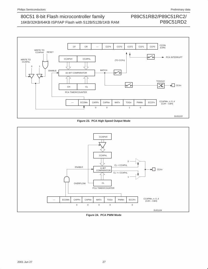
Philips Semiconductors Preliminary data
P89C51RB2/P89C51RC2/P89C51RD2
80C51 8-bit Flash microcontroller family16KB/32KB/64KB ISP/IAP Flash with 512B/512B/1KB RAM
2001 Jun 27 27
CF CR CCF4 CCF3 CCF2 CCF1 CCF0––CCON(C0H)
–– ECOMn CAPPn CAPNn MATn TOGn PWMn ECCFn CCAPMn, n: 0..4(C2H – C6H)
CH CL
CCAPnH CCAPnLPCA INTERRUPT
PCA TIMER/COUNTER
1 00 0
16–BIT COMPARATOR
(TO CCFn)
WRITE TO CCAPnH RESET
WRITE TO CCAPnL
0 1
ENABLE
CEXn
TOGGLE
MATCH
SU01103
Figure 23. PCA High Speed Output Mode
CL < CCAPnL
–– ECOMn CAPPn CAPNn MATn TOGn PWMn ECCFn CCAPMn, n: 0..4(C2H – C6H)
PCA TIMER/COUNTER
0 00 0
CL
CCAPnL
CEXn8–BIT
COMPARATOR
OVERFLOW
CCAPnH
ENABLE
0
1
CL >= CCAPnL
0
SU01104
Figure 24. PCA PWM Mode
Philips Semiconductors Preliminary data
P89C51RB2/P89C51RC2/P89C51RD2
80C51 8-bit Flash microcontroller family16KB/32KB/64KB ISP/IAP Flash with 512B/512B/1KB RAM
2001 Jun 27 28
–– ECOMn CAPPn CAPNn MATn TOGn PWMn ECCFn CCAPM4(C6H)
CH CL
CCAP4H CCAP4L
RESET
PCA TIMER/COUNTER
X 00 0
16–BIT COMPARATORMATCHENABLE
WRITE TO CCAP4L RESET
WRITE TO CCAP4H
1 0
1
CMOD(C1H)
CIDL WDTE –– –– –– CPS1 CPS0 ECF
X
SU01105
MODULE 4
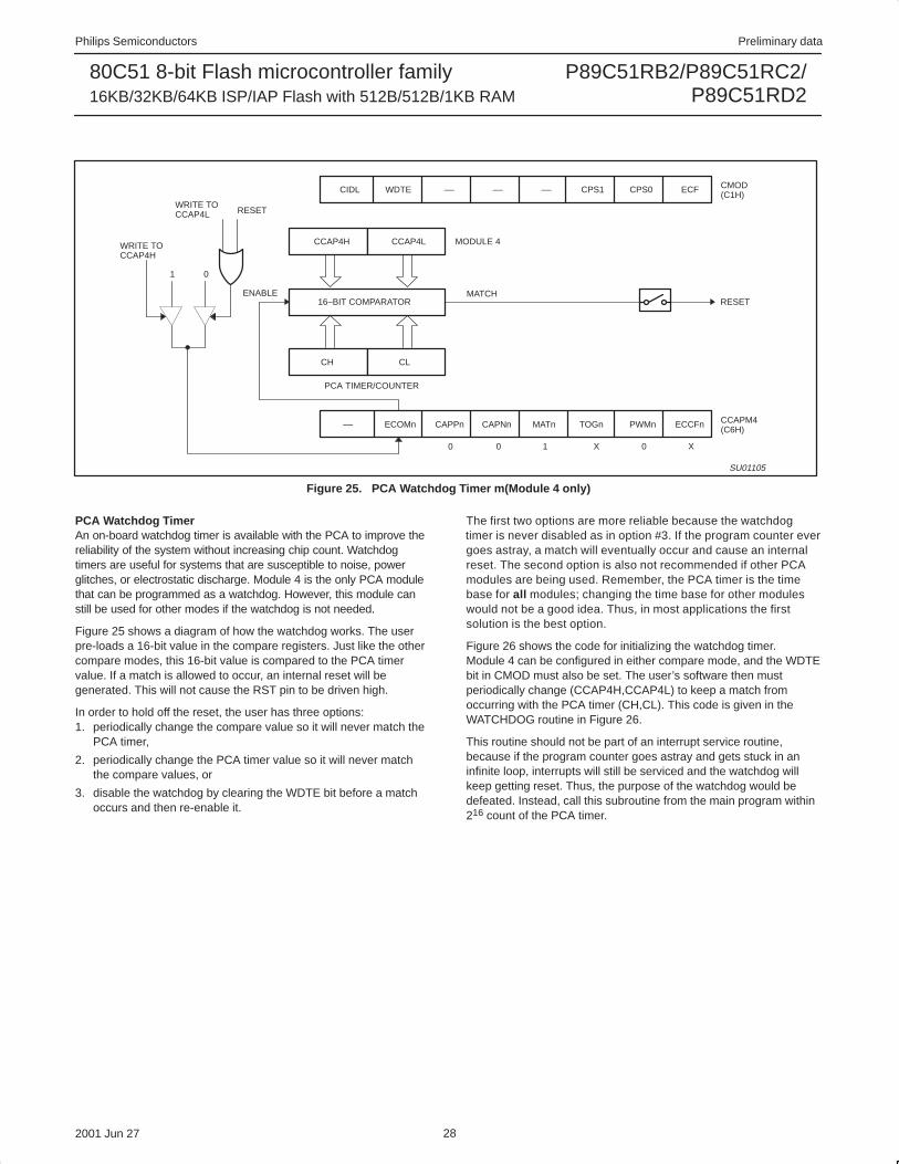
Figure 25. PCA Watchdog Timer m(Module 4 only)
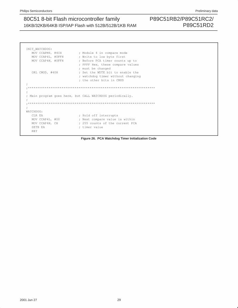
PCA Watchdog TimerAn on-board watchdog timer is available with the PCA to improve thereliability of the system without increasing chip count. Watchdogtimers are useful for systems that are susceptible to noise, powerglitches, or electrostatic discharge. Module 4 is the only PCA modulethat can be programmed as a watchdog. However, this module canstill be used for other modes if the watchdog is not needed.
Figure 25 shows a diagram of how the watchdog works. The userpre-loads a 16-bit value in the compare registers. Just like the othercompare modes, this 16-bit value is compared to the PCA timervalue. If a match is allowed to occur, an internal reset will begenerated. This will not cause the RST pin to be driven high.
In order to hold off the reset, the user has three options:1. periodically change the compare value so it will never match the
PCA timer,
2. periodically change the PCA timer value so it will never matchthe compare values, or
3. disable the watchdog by clearing the WDTE bit before a matchoccurs and then re-enable it.
The first two options are more reliable because the watchdogtimer is never disabled as in option #3. If the program counter evergoes astray, a match will eventually occur and cause an internalreset. The second option is also not recommended if other PCAmodules are being used. Remember, the PCA timer is the timebase for all modules; changing the time base for other moduleswould not be a good idea. Thus, in most applications the firstsolution is the best option.
Figure 26 shows the code for initializing the watchdog timer.Module 4 can be configured in either compare mode, and the WDTEbit in CMOD must also be set. The user’s software then mustperiodically change (CCAP4H,CCAP4L) to keep a match fromoccurring with the PCA timer (CH,CL). This code is given in theWATCHDOG routine in Figure 26.
This routine should not be part of an interrupt service routine,because if the program counter goes astray and gets stuck in aninfinite loop, interrupts will still be serviced and the watchdog willkeep getting reset. Thus, the purpose of the watchdog would bedefeated. Instead, call this subroutine from the main program within216 count of the PCA timer.
Philips Semiconductors Preliminary data
P89C51RB2/P89C51RC2/P89C51RD2
80C51 8-bit Flash microcontroller family16KB/32KB/64KB ISP/IAP Flash with 512B/512B/1KB RAM
2001 Jun 27 29
INIT_WATCHDOG: MOV CCAPM4, #4CH ; Module 4 in compare mode MOV CCAP4L, #0FFH ; Write to low byte first MOV CCAP4H, #0FFH ; Before PCA timer counts up to ; FFFF Hex, these compare values ; must be changed ORL CMOD, #40H ; Set the WDTE bit to enable the ; watchdog timer without changing ; the other bits in CMOD;;********************************************************************;; Main program goes here, but CALL WATCHDOG periodically.;;********************************************************************;WATCHDOG: CLR EA ; Hold off interrupts MOV CCAP4L, #00 ; Next compare value is within MOV CCAP4H, CH ; 255 counts of the current PCA SETB EA ; timer value RET
Figure 26. PCA Watchdog Timer Initialization Code
Philips Semiconductors Preliminary data
P89C51RB2/P89C51RC2/P89C51RD2
80C51 8-bit Flash microcontroller family16KB/32KB/64KB ISP/IAP Flash with 512B/512B/1KB RAM
2001 Jun 27 30
Expanded Data RAM AddressingThe P89C51RB2/RC2/RD2 has internal data memory that ismapped into four separate segments: the lower 128 bytes of RAM,upper 128 bytes of RAM, 128 bytes Special Function Register (SFR),and 256 bytes expanded RAM (ERAM) (768 bytes for the RD2).
The four segments are:1. The Lower 128 bytes of RAM (addresses 00H to 7FH) are
directly and indirectly addressable.
2. The Upper 128 bytes of RAM (addresses 80H to FFH) areindirectly addressable only.
3. The Special Function Registers, SFRs, (addresses 80H to FFH)are directly addressable only.
4. The 256/768-bytes expanded RAM (ERAM, 00H – 1FFH/2FFH)are indirectly accessed by move external instruction, MOVX, andwith the EXTRAM bit cleared, see Figure 27.
The Lower 128 bytes can be accessed by either direct or indirectaddressing. The Upper 128 bytes can be accessed by indirectaddressing only. The Upper 128 bytes occupy the same addressspace as the SFR. That means they have the same address, but arephysically separate from SFR space.
When an instruction accesses an internal location above address7FH, the CPU knows whether the access is to the upper 128 bytesof data RAM or to SFR space by the addressing mode used in theinstruction. Instructions that use direct addressing access SFRspace. For example:
MOV 0A0H,#data
accesses the SFR at location 0A0H (which is P2). Instructions thatuse indirect addressing access the Upper 128 bytes of data RAM.
For example:
MOV @R0,#data
where R0 contains 0A0H, accesses the data byte at address 0A0H,rather than P2 (whose address is 0A0H).
The ERAM can be accessed by indirect addressing, with EXTRAMbit cleared and MOVX instructions. This part of memory is physicallylocated on-chip, logically occupies the first 7936-bytes of externaldata memory.
With EXTRAM = 0, the ERAM is indirectly addressed, using theMOVX instruction in combination with any of the registers R0, R1 ofthe selected bank or DPTR. An access to ERAM will not affect portsP0, P3.6 (WR#) and P3.7 (RD#). P2 SFR is output during externaladdressing. For example, with EXTRAM = 0,
MOVX @R0,#data
where R0 contains 0A0H, access the ERAM at address 0A0H ratherthan external memory. An access to external data memory locationshigher than the ERAM will be performed with the MOVX DPTRinstructions in the same way as in the standard 80C51, so with P0and P2 as data/address bus, and P3.6 and P3.7 as write and readtiming signals. Refer to Figure 28.
With EXTRAM = 1, MOVX @Ri and MOVX @DPTR will be similarto the standard 80C51. MOVX @ Ri will provide an 8-bit addressmultiplexed with data on Port 0 and any output port pins can beused to output higher order address bits. This is to provide theexternal paging capability. MOVX @DPTR will generate a 16-bitaddress. Port 2 outputs the high-order eight address bits (thecontents of DPH) while Port 0 multiplexes the low-order eightaddress bits (DPL) with data. MOVX @Ri and MOVX @DPTR willgenerate either read or write signals on P3.6 (WR) and P3.7 (RD).
The stack pointer (SP) may be located anywhere in the 256 bytesRAM (lower and upper RAM) internal data memory. The stack maynot be located in the ERAM.
AUXR Reset Value = xxxx xx00B
— — — — — — EXTRAM AO
Not Bit Addressable
Bit:
Symbol Function
AO Disable/Enable ALE
AO Operating Mode0 ALE is emitted at a constant rate of 1/3 the oscillator frequency (6 clock mode; 1/6 fOSC in 12 clock mode).
1 ALE is active only during a MOVX or MOVC instruction.
EXTRAM Internal/External RAM access using MOVX @Ri/@DPTR
EXTRAM Operating Mode0 Internal ERAM access using MOVX @Ri/@DPTR1 External data memory access.
— Not implemented, reserved for future use*.
NOTE:*User software should not write 1s to reserved bits. These bits may be used in future 8051 family products to invoke new features. In that case, the reset or inactive value of the newbit will be 0, and its active value will be 1. The value read from a reserved bit is indeterminate.
SU01258
7 6 5 4 3 2 1 0
Address = 8EH
Figure 27. AUXR: Auxiliary Register
Philips Semiconductors Preliminary data
P89C51RB2/P89C51RC2/P89C51RD2
80C51 8-bit Flash microcontroller family16KB/32KB/64KB ISP/IAP Flash with 512B/512B/1KB RAM
2001 Jun 27 31
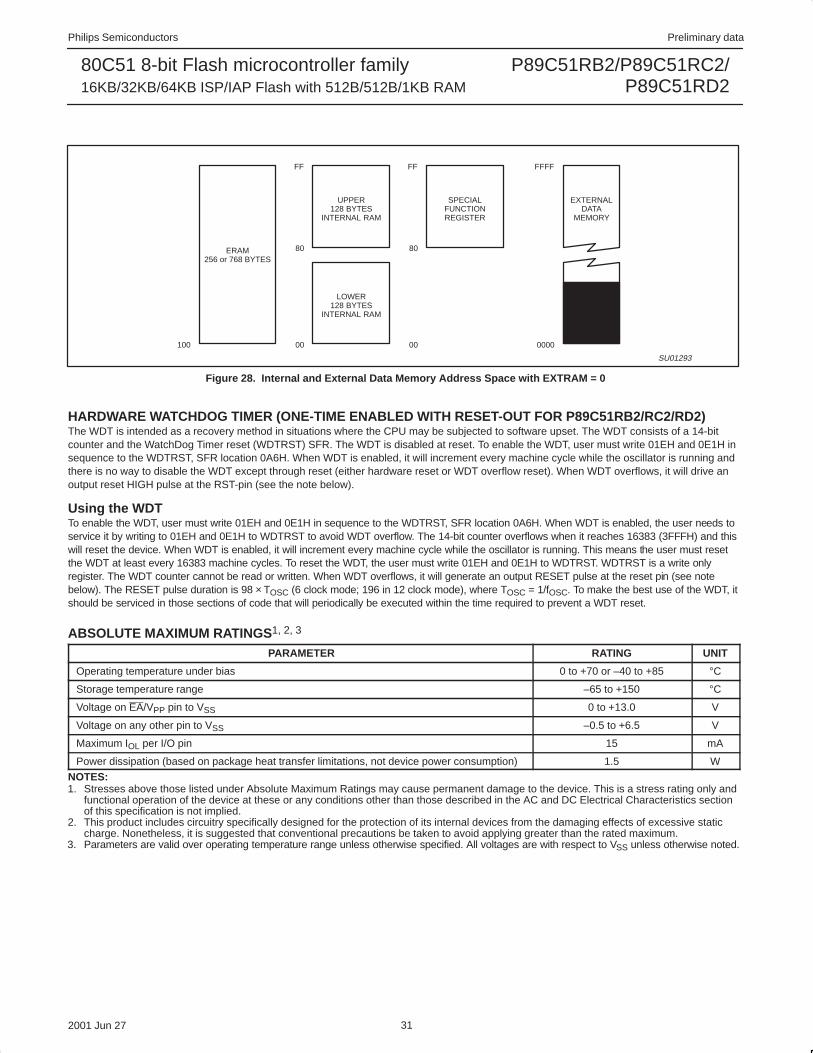
ERAM256 or 768 BYTES
UPPER128 BYTES
INTERNAL RAM
LOWER128 BYTES
INTERNAL RAM
SPECIALFUNCTIONREGISTER
100
FF
00
FF
00
80 80
EXTERNALDATA
MEMORY
FFFF
0000
SU01293
Figure 28. Internal and External Data Memory Address Space with EXTRAM = 0
HARDWARE WATCHDOG TIMER (ONE-TIME ENABLED WITH RESET-OUT FOR P89C51RB2/RC2/RD2)The WDT is intended as a recovery method in situations where the CPU may be subjected to software upset. The WDT consists of a 14-bitcounter and the WatchDog Timer reset (WDTRST) SFR. The WDT is disabled at reset. To enable the WDT, user must write 01EH and 0E1H insequence to the WDTRST, SFR location 0A6H. When WDT is enabled, it will increment every machine cycle while the oscillator is running andthere is no way to disable the WDT except through reset (either hardware reset or WDT overflow reset). When WDT overflows, it will drive anoutput reset HIGH pulse at the RST-pin (see the note below).
Using the WDTTo enable the WDT, user must write 01EH and 0E1H in sequence to the WDTRST, SFR location 0A6H. When WDT is enabled, the user needs toservice it by writing to 01EH and 0E1H to WDTRST to avoid WDT overflow. The 14-bit counter overflows when it reaches 16383 (3FFFH) and thiswill reset the device. When WDT is enabled, it will increment every machine cycle while the oscillator is running. This means the user must resetthe WDT at least every 16383 machine cycles. To reset the WDT, the user must write 01EH and 0E1H to WDTRST. WDTRST is a write onlyregister. The WDT counter cannot be read or written. When WDT overflows, it will generate an output RESET pulse at the reset pin (see notebelow). The RESET pulse duration is 98 × TOSC (6 clock mode; 196 in 12 clock mode), where TOSC = 1/fOSC. To make the best use of the WDT, itshould be serviced in those sections of code that will periodically be executed within the time required to prevent a WDT reset.
ABSOLUTE MAXIMUM RATINGS 1, 2, 3
PARAMETER RATING UNIT
Operating temperature under bias 0 to +70 or –40 to +85 °C
Storage temperature range –65 to +150 °C
Voltage on EA/VPP pin to VSS 0 to +13.0 V
Voltage on any other pin to VSS –0.5 to +6.5 V
Maximum IOL per I/O pin 15 mA
Power dissipation (based on package heat transfer limitations, not device power consumption) 1.5 W
NOTES:1. Stresses above those listed under Absolute Maximum Ratings may cause permanent damage to the device. This is a stress rating only and
functional operation of the device at these or any conditions other than those described in the AC and DC Electrical Characteristics sectionof this specification is not implied.
2. This product includes circuitry specifically designed for the protection of its internal devices from the damaging effects of excessive staticcharge. Nonetheless, it is suggested that conventional precautions be taken to avoid applying greater than the rated maximum.
3. Parameters are valid over operating temperature range unless otherwise specified. All voltages are with respect to VSS unless otherwise noted.
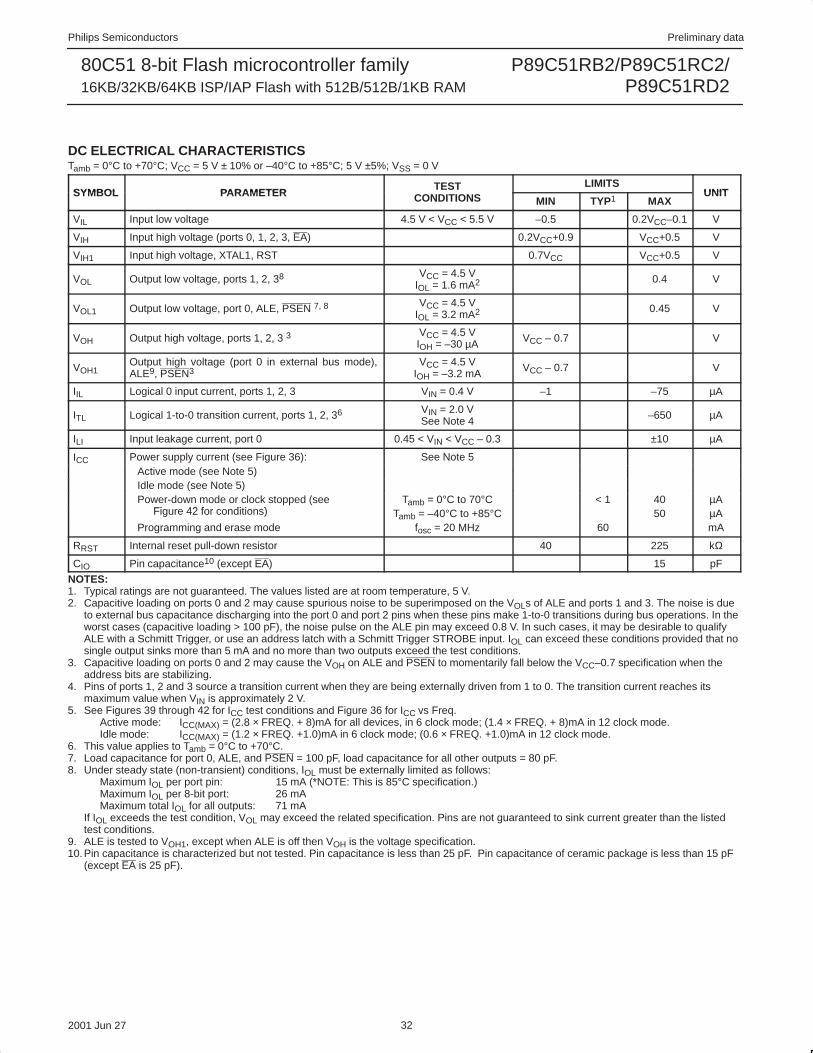
Philips Semiconductors Preliminary data
P89C51RB2/P89C51RC2/P89C51RD2
80C51 8-bit Flash microcontroller family16KB/32KB/64KB ISP/IAP Flash with 512B/512B/1KB RAM
2001 Jun 27 32
DC ELECTRICAL CHARACTERISTICSTamb = 0°C to +70°C; VCC = 5 V ± 10% or –40°C to +85°C; 5 V ±5%; VSS = 0 V
SYMBOL PARAMETERTEST LIMITS
UNITSYMBOL PARAMETER CONDITIONS MIN TYP1 MAXUNIT
VIL Input low voltage 4.5 V < VCC < 5.5 V –0.5 0.2VCC–0.1 V
VIH Input high voltage (ports 0, 1, 2, 3, EA) 0.2VCC+0.9 VCC+0.5 V
VIH1 Input high voltage, XTAL1, RST 0.7VCC VCC+0.5 V
VOL Output low voltage, ports 1, 2, 38 VCC = 4.5 VIOL = 1.6 mA2 0.4 V
VOL1 Output low voltage, port 0, ALE, PSEN 7, 8VCC = 4.5 V
IOL = 3.2 mA2 0.45 V
VOH Output high voltage, ports 1, 2, 3 3 VCC = 4.5 VIOH = –30 m A VCC – 0.7 V
VOH1Output high voltage (port 0 in external bus mode),ALE9, PSEN3
VCC = 4.5 VIOH = –3.2 mA VCC – 0.7 V
IIL Logical 0 input current, ports 1, 2, 3 VIN = 0.4 V –1 –75 m A
ITL Logical 1-to-0 transition current, ports 1, 2, 36 VIN = 2.0 VSee Note 4 –650 m A
ILI Input leakage current, port 0 0.45 < VIN < VCC – 0.3 ±10 m A
ICC Power supply current (see Figure 36): See Note 5Active mode (see Note 5)Idle mode (see Note 5)Power-down mode or clock stopped (see
Fi 42 f diti )Tamb = 0°C to 70°C < 1 40 m A
Figure 42 for conditions) Tamb = –40°C to +85°C 50 m AProgramming and erase mode fosc = 20 MHz 60 mA
RRST Internal reset pull-down resistor 40 225 k W
CIO Pin capacitance10 (except EA) 15 pF
NOTES:1. Typical ratings are not guaranteed. The values listed are at room temperature, 5 V.2. Capacitive loading on ports 0 and 2 may cause spurious noise to be superimposed on the VOLs of ALE and ports 1 and 3. The noise is due
to external bus capacitance discharging into the port 0 and port 2 pins when these pins make 1-to-0 transitions during bus operations. In theworst cases (capacitive loading > 100 pF), the noise pulse on the ALE pin may exceed 0.8 V. In such cases, it may be desirable to qualifyALE with a Schmitt Trigger, or use an address latch with a Schmitt Trigger STROBE input. IOL can exceed these conditions provided that nosingle output sinks more than 5 mA and no more than two outputs exceed the test conditions.
3. Capacitive loading on ports 0 and 2 may cause the VOH on ALE and PSEN to momentarily fall below the VCC–0.7 specification when theaddress bits are stabilizing.
4. Pins of ports 1, 2 and 3 source a transition current when they are being externally driven from 1 to 0. The transition current reaches itsmaximum value when VIN is approximately 2 V.
5. See Figures 39 through 42 for ICC test conditions and Figure 36 for ICC vs Freq. Active mode: ICC(MAX) = (2.8 × FREQ. + 8)mA for all devices, in 6 clock mode; (1.4 × FREQ. + 8)mA in 12 clock mode.Idle mode: ICC(MAX) = (1.2 × FREQ. +1.0)mA in 6 clock mode; (0.6 × FREQ. +1.0)mA in 12 clock mode.
6. This value applies to Tamb = 0°C to +70°C.7. Load capacitance for port 0, ALE, and PSEN = 100 pF, load capacitance for all other outputs = 80 pF.8. Under steady state (non-transient) conditions, IOL must be externally limited as follows:
Maximum IOL per port pin: 15 mA (*NOTE: This is 85°C specification.)Maximum IOL per 8-bit port: 26 mAMaximum total IOL for all outputs: 71 mA
If IOL exceeds the test condition, VOL may exceed the related specification. Pins are not guaranteed to sink current greater than the listedtest conditions.
9. ALE is tested to VOH1, except when ALE is off then VOH is the voltage specification.10.Pin capacitance is characterized but not tested. Pin capacitance is less than 25 pF. Pin capacitance of ceramic package is less than 15 pF
(except EA is 25 pF).
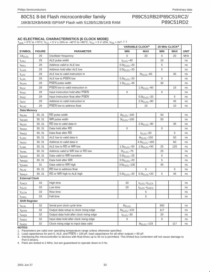
Philips Semiconductors Preliminary data
P89C51RB2/P89C51RC2/P89C51RD2
80C51 8-bit Flash microcontroller family16KB/32KB/64KB ISP/IAP Flash with 512B/512B/1KB RAM
2001 Jun 27 33
AC ELECTRICAL CHARACTERISTICS (6 CLOCK MODE)Tamb = 0°C to +70°C; VCC = 5 V ± 10% or –40°C to +85°C, VCC = 5 V ±5%, VSS = 0V1, 2, 3
VARIABLE CLOCK 4 20 MHz CLOCK4
SYMBOL FIGURE PARAMETER MIN MAX MIN MAX UNIT
1/tCLCL 29 Oscillator frequency 0 20 0 20 MHz
tLHLL 29 ALE pulse width tCLCL–40 10 ns
tAVLL 29 Address valid to ALE low 0.5tCLCL–20 5 ns
tLLAX 29 Address hold after ALE low 0.5tCLCL–20 5 ns
tLLIV 29 ALE low to valid instruction in 2tCLCL–65 35 ns
tLLPL 29 ALE low to PSEN low 0.5tCLCL–20 5 ns
tPLPH 29 PSEN pulse width 1.5tCLCL–45 30 ns
tPLIV 29 PSEN low to valid instruction in 1.5tCLCL–60 15 ns
tPXIX 29 Input instruction hold after PSEN 0 0 ns
tPXIZ 29 Input instruction float after PSEN 0.5tCLCL–20 5 ns
tAVIV 29 Address to valid instruction in 2.5tCLCL–80 45 ns
tPLAZ 29 PSEN low to address float 10 10 ns
Data Memory
tRLRH 30, 31 RD pulse width 3tCLCL–100 50 ns
tWLWH 30, 31 WR pulse width 3tCLCL–100 50 ns
tRLDV 30, 31 RD low to valid data in 2.5tCLCL–90 35 ns
tRHDX 30, 31 Data hold after RD 0 0 ns
tRHDZ 30, 31 Data float after RD tCLCL–20 5 ns
tLLDV 30, 31 ALE low to valid data in 4tCLCL–150 50 ns
tAVDV 30, 31 Address to valid data in 4.5tCLCL–165 60 ns
tLLWL 30, 31 ALE low to RD or WR low 1.5tCLCL–50 1.5tCLCL+50 25 125 ns
tAVWL 30, 31 Address valid to WR low or RD low 2tCLCL–75 25 ns
tQVWX 30, 31 Data valid to WR transition 0.5tCLCL–25 0 ns
tWHQX 30, 31 Data hold after WR 0.5tCLCL–20 5 ns
tQVWH 31 Data valid to WR high 3.5tCLCL–130 45 ns
tRLAZ 30, 31 RD low to address float 0 0 ns
tWHLH 30, 31 RD or WR high to ALE high 0.5tCLCL–20 0.5tCLCL+20 5 45 ns
External Clock
tCHCX 33 High time 20 tCLCL–tCLCX ns
tCLCX 33 Low time 20 tCLCL–tCHCX ns
tCLCH 33 Rise time 5 ns
tCHCL 33 Fall time 5 ns
Shift Register
tXLXL 32 Serial port clock cycle time 6tCLCL 300 ns
tQVXH 32 Output data setup to clock rising edge 5tCLCL–133 117 ns
tXHQX 32 Output data hold after clock rising edge tCLCL–30 20 ns
tXHDX 32 Input data hold after clock rising edge 0 0 ns
tXHDV 32 Clock rising edge to input data valid 5tCLCL–133 117 nsNOTES:1. Parameters are valid over operating temperature range unless otherwise specified.2. Load capacitance for port 0, ALE, and PSEN = 100 pF, load capacitance for all other outputs = 80 pF.3. Interfacing the microcontroller to devices with float times up to 45 ns is permitted. This limited bus contention will not cause damage to
Port 0 drivers.4. Parts are tested to 2 MHz, but are guaranteed to operate down to 0 Hz.
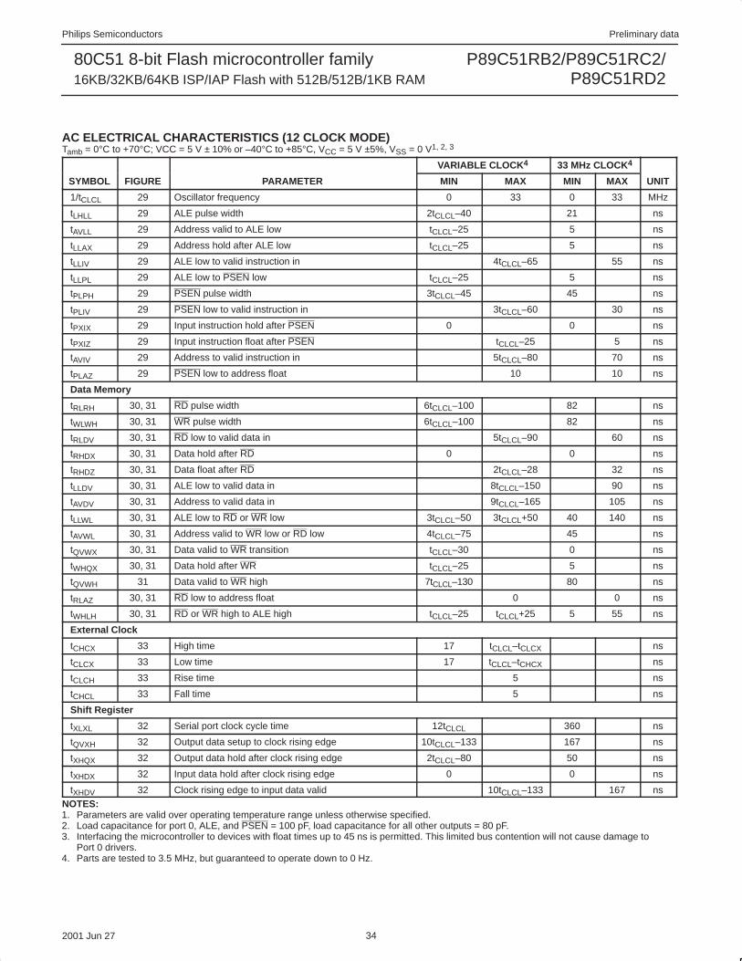
Philips Semiconductors Preliminary data
P89C51RB2/P89C51RC2/P89C51RD2
80C51 8-bit Flash microcontroller family16KB/32KB/64KB ISP/IAP Flash with 512B/512B/1KB RAM
2001 Jun 27 34
AC ELECTRICAL CHARACTERISTICS (12 CLOCK MODE)Tamb = 0°C to +70°C; VCC = 5 V ± 10% or –40°C to +85°C, VCC = 5 V ±5%, VSS = 0 V1, 2, 3
VARIABLE CLOCK 4 33 MHz CLOCK4
SYMBOL FIGURE PARAMETER MIN MAX MIN MAX UNIT
1/tCLCL 29 Oscillator frequency 0 33 0 33 MHz
tLHLL 29 ALE pulse width 2tCLCL–40 21 ns
tAVLL 29 Address valid to ALE low tCLCL–25 5 ns
tLLAX 29 Address hold after ALE low tCLCL–25 5 ns
tLLIV 29 ALE low to valid instruction in 4tCLCL–65 55 ns
tLLPL 29 ALE low to PSEN low tCLCL–25 5 ns
tPLPH 29 PSEN pulse width 3tCLCL–45 45 ns
tPLIV 29 PSEN low to valid instruction in 3tCLCL–60 30 ns
tPXIX 29 Input instruction hold after PSEN 0 0 ns
tPXIZ 29 Input instruction float after PSEN tCLCL–25 5 ns
tAVIV 29 Address to valid instruction in 5tCLCL–80 70 ns
tPLAZ 29 PSEN low to address float 10 10 ns
Data Memory
tRLRH 30, 31 RD pulse width 6tCLCL–100 82 ns
tWLWH 30, 31 WR pulse width 6tCLCL–100 82 ns
tRLDV 30, 31 RD low to valid data in 5tCLCL–90 60 ns
tRHDX 30, 31 Data hold after RD 0 0 ns
tRHDZ 30, 31 Data float after RD 2tCLCL–28 32 ns
tLLDV 30, 31 ALE low to valid data in 8tCLCL–150 90 ns
tAVDV 30, 31 Address to valid data in 9tCLCL–165 105 ns
tLLWL 30, 31 ALE low to RD or WR low 3tCLCL–50 3tCLCL+50 40 140 ns
tAVWL 30, 31 Address valid to WR low or RD low 4tCLCL–75 45 ns
tQVWX 30, 31 Data valid to WR transition tCLCL–30 0 ns
tWHQX 30, 31 Data hold after WR tCLCL–25 5 ns
tQVWH 31 Data valid to WR high 7tCLCL–130 80 ns
tRLAZ 30, 31 RD low to address float 0 0 ns
tWHLH 30, 31 RD or WR high to ALE high tCLCL–25 tCLCL+25 5 55 ns
External Clock
tCHCX 33 High time 17 tCLCL–tCLCX ns
tCLCX 33 Low time 17 tCLCL–tCHCX ns
tCLCH 33 Rise time 5 ns
tCHCL 33 Fall time 5 ns
Shift Register
tXLXL 32 Serial port clock cycle time 12tCLCL 360 ns
tQVXH 32 Output data setup to clock rising edge 10tCLCL–133 167 ns
tXHQX 32 Output data hold after clock rising edge 2tCLCL–80 50 ns
tXHDX 32 Input data hold after clock rising edge 0 0 ns
tXHDV 32 Clock rising edge to input data valid 10tCLCL–133 167 nsNOTES:1. Parameters are valid over operating temperature range unless otherwise specified.2. Load capacitance for port 0, ALE, and PSEN = 100 pF, load capacitance for all other outputs = 80 pF.3. Interfacing the microcontroller to devices with float times up to 45 ns is permitted. This limited bus contention will not cause damage to
Port 0 drivers.4. Parts are tested to 3.5 MHz, but guaranteed to operate down to 0 Hz.
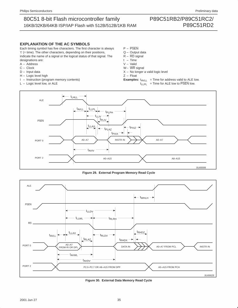
Philips Semiconductors Preliminary data
P89C51RB2/P89C51RC2/P89C51RD2
80C51 8-bit Flash microcontroller family16KB/32KB/64KB ISP/IAP Flash with 512B/512B/1KB RAM
2001 Jun 27 35
EXPLANATION OF THE AC SYMBOLSEach timing symbol has five characters. The first character is always‘t’ (= time). The other characters, depending on their positions,indicate the name of a signal or the logical status of that signal. Thedesignations are:A – AddressC – ClockD – Input dataH – Logic level highI – Instruction (program memory contents)L – Logic level low, or ALE
P – PSENQ – Output dataR – RD signalt – TimeV – ValidW– WR signalX – No longer a valid logic levelZ – FloatExamples: tAVLL = Time for address valid to ALE low.
tLLPL = Time for ALE low to PSEN low.
tPXIZ
ALE
PSEN
PORT 0
PORT 2 A0–A15 A8–A15
A0–A7 A0–A7
tAVLL
tPXIX
tLLAX
INSTR IN
tLHLL
tPLPHtLLIV
tPLAZ
tLLPL
tAVIV
SU00006
tPLIV
Figure 29. External Program Memory Read Cycle
ALE
PSEN
PORT 0
PORT 2
RD
A0–A7FROM RI OR DPL DATA IN A0–A7 FROM PCL INSTR IN
P2.0–P2.7 OR A8–A15 FROM DPF A0–A15 FROM PCH
tWHLH
tLLDV
tLLWL tRLRH
tLLAX
tRLAZ
tAVLL
tRHDX
tRHDZ
tAVWL
tAVDV
tRLDV
SU00025
Figure 30. External Data Memory Read Cycle
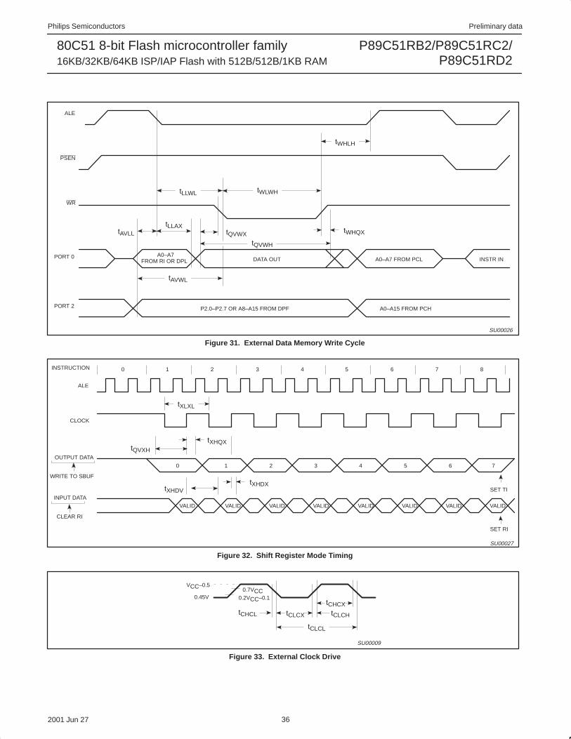
Philips Semiconductors Preliminary data
P89C51RB2/P89C51RC2/P89C51RD2
80C51 8-bit Flash microcontroller family16KB/32KB/64KB ISP/IAP Flash with 512B/512B/1KB RAM
2001 Jun 27 36
tLLAX
ALE
PSEN
PORT 0
PORT 2
WR
A0–A7FROM RI OR DPL DATA OUT A0–A7 FROM PCL INSTR IN
P2.0–P2.7 OR A8–A15 FROM DPF A0–A15 FROM PCH
tWHLH
tLLWL tWLWH
tAVLL
tAVWL
tQVWX tWHQX
tQVWH
SU00026
Figure 31. External Data Memory Write Cycle
0 1 2 3 4 5 6 7 8INSTRUCTION
ALE
CLOCK
OUTPUT DATA
WRITE TO SBUF
INPUT DATA
CLEAR RI
VALID VALID VALID VALID VALID VALID VALID VALID
SET TI
SET RI
tXLXL
tQVXH
tXHQX
tXHDXtXHDV
SU00027
1 2 30 4 5 6 7
Figure 32. Shift Register Mode Timing
VCC–0.5
0.45V0.7VCC
0.2VCC–0.1
tCHCL
tCLCL
tCLCHtCLCX
tCHCX
SU00009
Figure 33. External Clock Drive
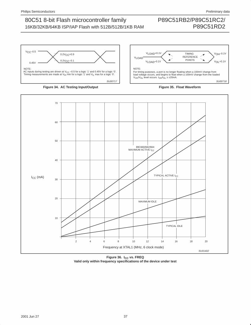
Philips Semiconductors Preliminary data
P89C51RB2/P89C51RC2/P89C51RD2
80C51 8-bit Flash microcontroller family16KB/32KB/64KB ISP/IAP Flash with 512B/512B/1KB RAM
2001 Jun 27 37
VCC–0.5
0.45V
0.2VCC+0.9
0.2VCC–0.1
NOTE:AC inputs during testing are driven at VCC –0.5 for a logic ‘1’ and 0.45V for a logic ‘0’.Timing measurements are made at VIH min for a logic ‘1’ and VIL max for a logic ‘0’.
SU00717
Figure 34. AC Testing Input/Output
VLOAD
VLOAD+0.1V
VLOAD–0.1V
VOH–0.1V
VOL+0.1V
NOTE:
TIMINGREFERENCE
POINTS
For timing purposes, a port is no longer floating when a 100mV change fromload voltage occurs, and begins to float when a 100mV change from the loadedVOH/VOL level occurs. IOH/IOL ≥ ±20mA.
SU00718
Figure 35. Float Waveform
2 4 6 8 10 12 14 16 18
60
50
40
30
20
10
Frequency at XTAL1 (MHz, 6 clock mode)
ICC (mA)
89C660/662/664MAXIMUM ACTIVE ICC
TYPICAL ACTIVE ICC
MAXIMUM IDLE
TYPICAL IDLE
SU01402
20
70
Figure 36. I CC vs. FREQValid only within frequency specifications of the device under test
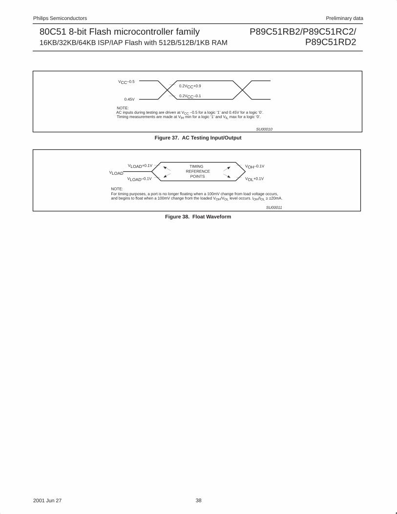
Philips Semiconductors Preliminary data
P89C51RB2/P89C51RC2/P89C51RD2
80C51 8-bit Flash microcontroller family16KB/32KB/64KB ISP/IAP Flash with 512B/512B/1KB RAM
2001 Jun 27 38
VCC–0.5
0.45V
0.2VCC+0.9
0.2VCC–0.1
NOTE:AC inputs during testing are driven at VCC –0.5 for a logic ‘1’ and 0.45V for a logic ‘0’.Timing measurements are made at VIH min for a logic ‘1’ and VIL max for a logic ‘0’.
SU00010
Figure 37. AC Testing Input/Output
VLOAD
VLOAD+0.1V
VLOAD–0.1V
VOH–0.1V
VOL+0.1V
NOTE:
TIMINGREFERENCE
POINTS
For timing purposes, a port is no longer floating when a 100mV change from load voltage occurs,and begins to float when a 100mV change from the loaded VOH/VOL level occurs. IOH/IOL ≥ ±20mA.
SU00011
Figure 38. Float Waveform
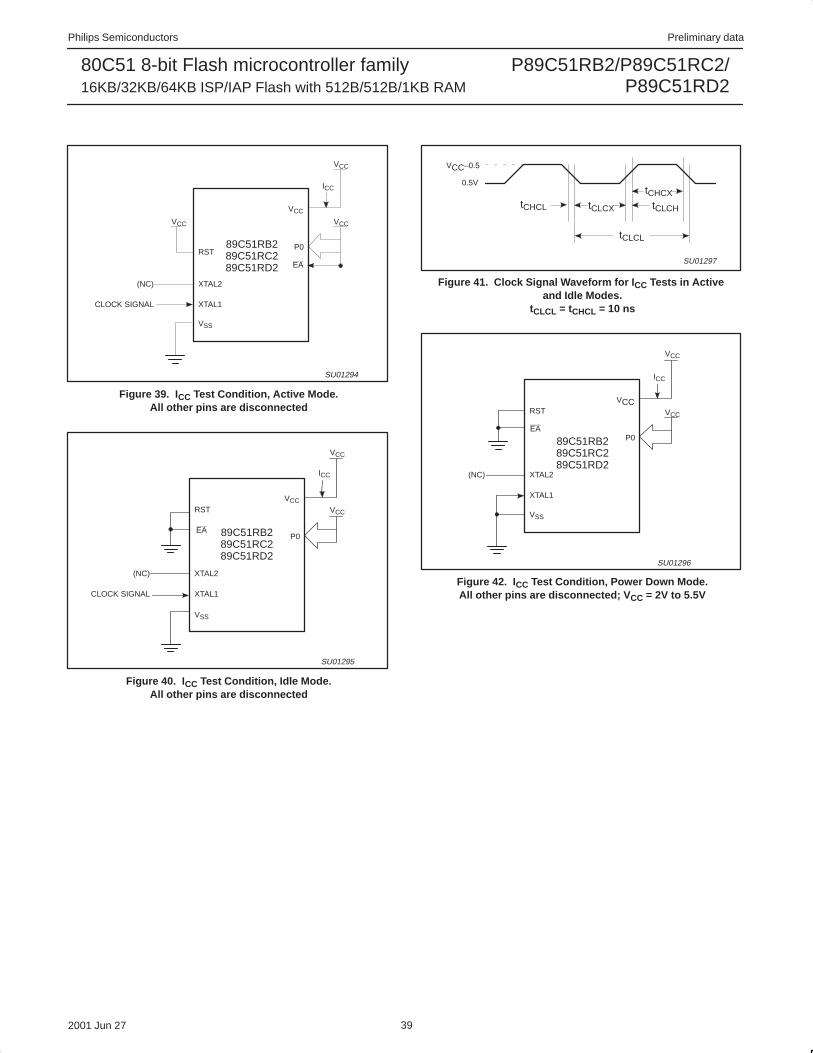
Philips Semiconductors Preliminary data
P89C51RB2/P89C51RC2/P89C51RD2
80C51 8-bit Flash microcontroller family16KB/32KB/64KB ISP/IAP Flash with 512B/512B/1KB RAM
2001 Jun 27 39
VCC
P0
EA
RST
XTAL1
XTAL2
VSS
VCC
VCC
VCC
ICC
(NC)
CLOCK SIGNAL
89C51RB289C51RC289C51RD2
SU01294
Figure 39. I CC Test Condition, Active Mode.All other pins are disconnected
VCC
P0
RST
XTAL1
XTAL2
VSS
VCC
VCC
ICC
(NC)
CLOCK SIGNAL
EA
SU01295
89C51RB289C51RC289C51RD2
Figure 40. I CC Test Condition, Idle Mode.All other pins are disconnected
VCC–0.5
0.5V
tCHCL
tCLCL
tCLCHtCLCX
tCHCX
SU01297
Figure 41. Clock Signal Waveform for I CC Tests in Active and Idle Modes.
tCLCL = tCHCL = 10 ns
VCC
P0
RST
XTAL1
XTAL2
VSS
VCC
VCC
ICC
(NC)
EA
SU01296
89C51RB289C51RC289C51RD2
Figure 42. I CC Test Condition, Power Down Mode.All other pins are disconnected; V CC = 2V to 5.5V
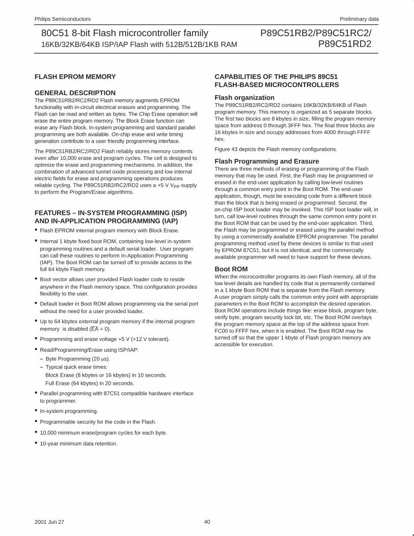
Philips Semiconductors Preliminary data
P89C51RB2/P89C51RC2/P89C51RD2
80C51 8-bit Flash microcontroller family16KB/32KB/64KB ISP/IAP Flash with 512B/512B/1KB RAM
2001 Jun 27 40
FLASH EPROM MEMORY
GENERAL DESCRIPTIONThe P89C51RB2/RC2/RD2 Flash memory augments EPROMfunctionality with in-circuit electrical erasure and programming. TheFlash can be read and written as bytes. The Chip Erase operation willerase the entire program memory. The Block Erase function canerase any Flash block. In-system programming and standard parallelprogramming are both available. On-chip erase and write timinggeneration contribute to a user friendly programming interface.
The P89C51RB2/RC2/RD2 Flash reliably stores memory contentseven after 10,000 erase and program cycles. The cell is designed tooptimize the erase and programming mechanisms. In addition, thecombination of advanced tunnel oxide processing and low internalelectric fields for erase and programming operations producesreliable cycling. The P89C51RB2/RC2/RD2 uses a +5 V VPP supplyto perform the Program/Erase algorithms.
FEATURES – IN-SYSTEM PROGRAMMING (ISP)AND IN-APPLICATION PROGRAMMING (IAP)• Flash EPROM internal program memory with Block Erase.
• Internal 1 kbyte fixed boot ROM, containing low-level in-systemprogramming routines and a default serial loader. User programcan call these routines to perform In-Application Programming(IAP). The Boot ROM can be turned off to provide access to thefull 64 kbyte Flash memory.
• Boot vector allows user provided Flash loader code to resideanywhere in the Flash memory space. This configuration providesflexibility to the user.
• Default loader in Boot ROM allows programming via the serial portwithout the need for a user provided loader.
• Up to 64 kbytes external program memory if the internal programmemory is disabled (EA = 0).
• Programming and erase voltage +5 V (+12 V tolerant).
• Read/Programming/Erase using ISP/IAP:
– Byte Programming (20 �s).
– Typical quick erase times:
Block Erase (8 kbytes or 16 kbytes) in 10 seconds.
Full Erase (64 kbytes) in 20 seconds.
• Parallel programming with 87C51 compatible hardware interfaceto programmer.
• In-system programming.
• Programmable security for the code in the Flash.
• 10,000 minimum erase/program cycles for each byte.
• 10-year minimum data retention.
CAPABILITIES OF THE PHILIPS 89C51FLASH-BASED MICROCONTROLLERS
Flash organizationThe P89C51RB2/RC2/RD2 contains 16KB/32KB/64KB of Flashprogram memory. This memory is organized as 5 separate blocks.The first two blocks are 8 kbytes in size, filling the program memoryspace from address 0 through 3FFF hex. The final three blocks are16 kbytes in size and occupy addresses from 4000 through FFFFhex.
Figure 43 depicts the Flash memory configurations.
Flash Programming and ErasureThere are three methods of erasing or programming of the Flashmemory that may be used. First, the Flash may be programmed orerased in the end-user application by calling low-level routinesthrough a common entry point in the Boot ROM. The end-userapplication, though, must be executing code from a different blockthan the block that is being erased or programmed. Second, theon-chip ISP boot loader may be invoked. This ISP boot loader will, inturn, call low-level routines through the same common entry point inthe Boot ROM that can be used by the end-user application. Third,the Flash may be programmed or erased using the parallel methodby using a commercially available EPROM programmer. The parallelprogramming method used by these devices is similar to that usedby EPROM 87C51, but it is not identical, and the commerciallyavailable programmer will need to have support for these devices.
Boot ROMWhen the microcontroller programs its own Flash memory, all of thelow level details are handled by code that is permanently containedin a 1 kbyte Boot ROM that is separate from the Flash memory.A user program simply calls the common entry point with appropriateparameters in the Boot ROM to accomplish the desired operation.Boot ROM operations include things like: erase block, program byte,verify byte, program security lock bit, etc. The Boot ROM overlaysthe program memory space at the top of the address space fromFC00 to FFFF hex, when it is enabled. The Boot ROM may beturned off so that the upper 1 kbyte of Flash program memory areaccessible for execution.
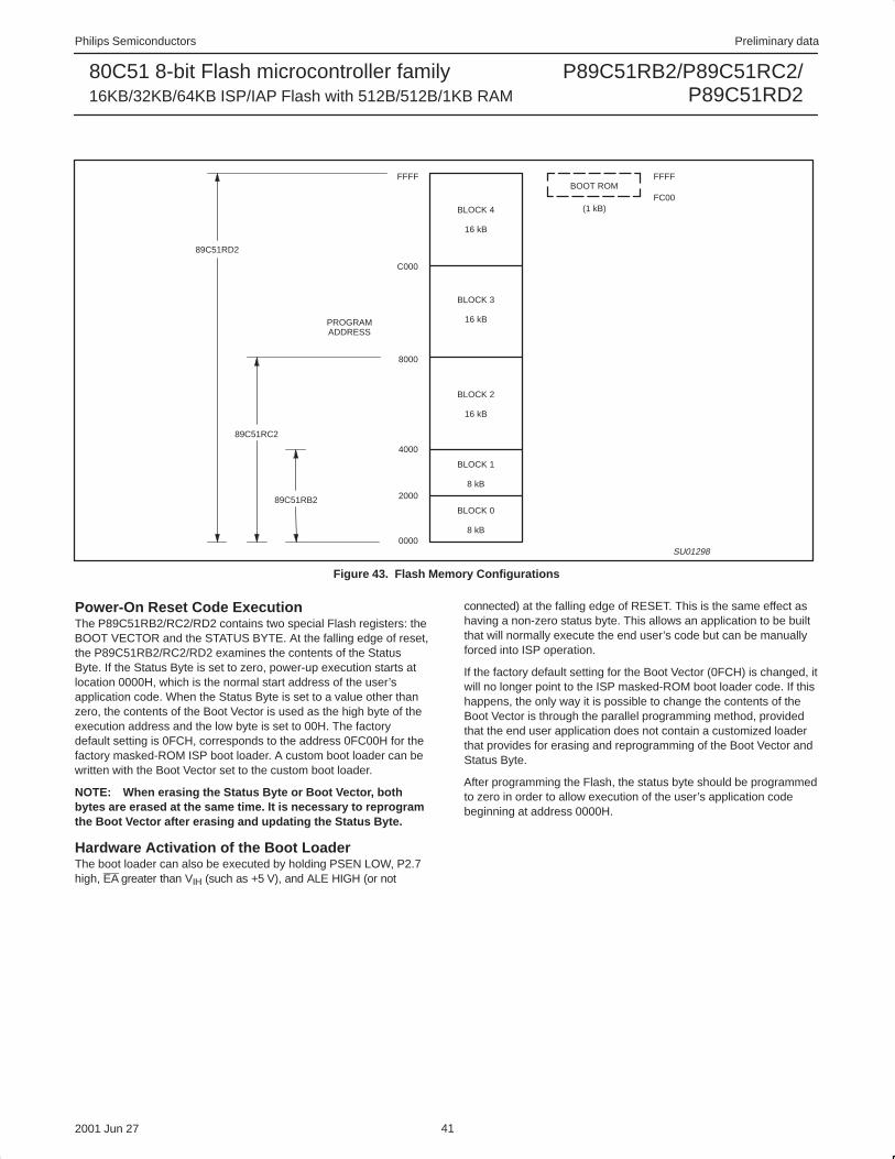
Philips Semiconductors Preliminary data
P89C51RB2/P89C51RC2/P89C51RD2
80C51 8-bit Flash microcontroller family16KB/32KB/64KB ISP/IAP Flash with 512B/512B/1KB RAM
2001 Jun 27 41
FFFF
C000
8000
4000
2000
0000
BLOCK 4
16 kB
BLOCK 3
16 kB
BLOCK 2
16 kB
BLOCK 1
8 kB
BLOCK 0
8 kB
PROGRAMADDRESS
BOOT ROM
(1 kB)
FFFF
FC00
SU01298
89C51RD2
89C51RC2
89C51RB2
Figure 43. Flash Memory Configurations
Power-On Reset Code ExecutionThe P89C51RB2/RC2/RD2 contains two special Flash registers: theBOOT VECTOR and the STATUS BYTE. At the falling edge of reset,the P89C51RB2/RC2/RD2 examines the contents of the StatusByte. If the Status Byte is set to zero, power-up execution starts atlocation 0000H, which is the normal start address of the user’sapplication code. When the Status Byte is set to a value other thanzero, the contents of the Boot Vector is used as the high byte of theexecution address and the low byte is set to 00H. The factorydefault setting is 0FCH, corresponds to the address 0FC00H for thefactory masked-ROM ISP boot loader. A custom boot loader can bewritten with the Boot Vector set to the custom boot loader.
NOTE: When erasing the Status Byte or Boot Vector, bothbytes are erased at the same time. It is necessary to reprogramthe Boot Vector after erasing and updating the Status Byte.
Hardware Activation of the Boot LoaderThe boot loader can also be executed by holding PSEN LOW, P2.7high, EA greater than VIH (such as +5 V), and ALE HIGH (or not
connected) at the falling edge of RESET. This is the same effect ashaving a non-zero status byte. This allows an application to be builtthat will normally execute the end user’s code but can be manuallyforced into ISP operation.
If the factory default setting for the Boot Vector (0FCH) is changed, itwill no longer point to the ISP masked-ROM boot loader code. If thishappens, the only way it is possible to change the contents of theBoot Vector is through the parallel programming method, providedthat the end user application does not contain a customized loaderthat provides for erasing and reprogramming of the Boot Vector andStatus Byte.
After programming the Flash, the status byte should be programmedto zero in order to allow execution of the user’s application codebeginning at address 0000H.
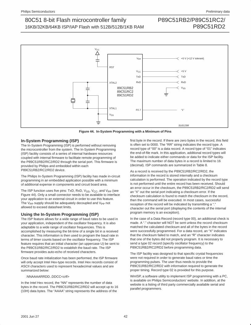
Philips Semiconductors Preliminary data
P89C51RB2/P89C51RC2/P89C51RD2
80C51 8-bit Flash microcontroller family16KB/32KB/64KB ISP/IAP Flash with 512B/512B/1KB RAM
2001 Jun 27 42
+5 V (+12 V tolerant)
+5 V
TxD
RxD
VSS
VPP
VCC
TxD
RxD
RST
XTAL2
XTAL1
SU01299
VSS
VCC
89C51RB289C51RC289C51RD2
“1”P2.7
Figure 44. In-System Programming with a Minimum of Pins
In-System Programming (ISP)The In-System Programming (ISP) is performed without removingthe microcontroller from the system. The In-System Programming(ISP) facility consists of a series of internal hardware resourcescoupled with internal firmware to facilitate remote programming ofthe P89C51RB2/RC2/RD2 through the serial port. This firmware isprovided by Philips and embedded within eachP89C51RB2/RC2/RD2 device.
The Philips In-System Programming (ISP) facility has made in-circuitprogramming in an embedded application possible with a minimumof additional expense in components and circuit board area.
The ISP function uses five pins: TxD, RxD, VSS, VCC, and VPP (seeFigure 44). Only a small connector needs to be available to interfaceyour application to an external circuit in order to use this feature.The VPP supply should be adequately decoupled and VPP notallowed to exceed datasheet limits.
Using the In-System Programming (ISP)The ISP feature allows for a wide range of baud rates to be used inyour application, independent of the oscillator frequency. It is alsoadaptable to a wide range of oscillator frequencies. This isaccomplished by measuring the bit-time of a single bit in a receivedcharacter. This information is then used to program the baud rate interms of timer counts based on the oscillator frequency. The ISPfeature requires that an initial character (an uppercase U) be sent tothe P89C51RB2/RC2/RD2 to establish the baud rate. The ISPfirmware provides auto-echo of received characters.
Once baud rate initialization has been performed, the ISP firmwarewill only accept Intel Hex-type records. Intel Hex records consist ofASCII characters used to represent hexadecimal values and aresummarized below:
:NNAAAARRDD..DDCC<crlf>
In the Intel Hex record, the “NN” represents the number of databytes in the record. The P89C51RB2/RC2/RD2 will accept up to 16(10H) data bytes. The “AAAA” string represents the address of the
first byte in the record. If there are zero bytes in the record, this fieldis often set to 0000. The “RR” string indicates the record type. Arecord type of “00” is a data record. A record type of “01” indicatesthe end-of-file mark. In this application, additional record types willbe added to indicate either commands or data for the ISP facility.The maximum number of data bytes in a record is limited to 16(decimal). ISP commands are summarized in Table 8.
As a record is received by the P89C51RB2/RC2/RD2, theinformation in the record is stored internally and a checksumcalculation is performed. The operation indicated by the record typeis not performed until the entire record has been received. Shouldan error occur in the checksum, the P89C51RB2/RC2/RD2 will sendan “X” out the serial port indicating a checksum error. If thechecksum calculation is found to match the checksum in the record,then the command will be executed. In most cases, successfulreception of the record will be indicated by transmitting a “.”character out the serial port (displaying the contents of the internalprogram memory is an exception).
In the case of a Data Record (record type 00), an additional check ismade. A “.” character will NOT be sent unless the record checksummatched the calculated checksum and all of the bytes in the recordwere successfully programmed. For a data record, an “X” indicatesthat the checksum failed to match, and an “R” character indicatesthat one of the bytes did not properly program. It is necessary tosend a type 02 record (specify oscillator frequency) to theP89C51RB2/RC2/RD2 before programming data.
The ISP facility was designed to that specific crystal frequencieswere not required in order to generate baud rates or time theprogramming pulses. The user thus needs to provide theP89C51RB2/RC2/RD2 with information required to generate theproper timing. Record type 02 is provided for this purpose.
WinISP, a software utility to implement ISP programming with a PC,is available on Philips Semiconductors’ website. In addition, at thewebsite is a listing of third party commercially available serial andparallel programmers.
Philips Semiconductors Preliminary data
P89C51RB2/P89C51RC2/P89C51RD2
80C51 8-bit Flash microcontroller family16KB/32KB/64KB ISP/IAP Flash with 512B/512B/1KB RAM
2001 Jun 27 43
Table 8. Intel-Hex Records Used by In-System ProgrammingRECORD TYPE COMMAND/DATA FUNCTION
00 Program Data:nnaaaa00dd....ddcc
Where:Nn = number of bytes (hex) in recordAaaa = memory address of first byte in recorddd....dd = data bytescc = checksum
Example::10008000AF5F67F0602703E0322CFA92007780C3FD
01 End of File (EOF), no operation:xxxxxx01cc
Where:xxxxxx = required field, but value is a “don’t care”cc = checksum
Example::00000001FF
02 Specify Oscillator Frequency:01xxxx02ddcc
Where:xxxx = required field, but value is a “don’t care”dd = integer oscillator frequency rounded down to nearest MHzcc = checksum
Example::0100000210ED (dd = 10h = 16, used for 16.0–16.9 MHz)
Philips Semiconductors Preliminary data
P89C51RB2/P89C51RC2/P89C51RD2
80C51 8-bit Flash microcontroller family16KB/32KB/64KB ISP/IAP Flash with 512B/512B/1KB RAM
2001 Jun 27 44
RECORD TYPE COMMAND/DATA FUNCTION
03 Miscellaneous Write Functions:nnxxxx03ffssddcc
Where:nn = number of bytes (hex) in recordxxxx = required field, but value is a “don’t care”03 = Write Functionff = subfunction codess = selection codedd = data input (as needed)cc = checksum
Subfunction Code = 01 (Erase Blocks)ff = 01ss = block code as shown below: block 0, 0k to 8k, 00H block 1, 8k to 16k, 20H block 2, 16k to 32k, 40H block 3, 32k to 48k, 80H block 4, 48k to 64k, C0HExample: :0200000301C03A erase block 4
Subfunction Code = 04 (Erase Boot Vector and Status Byte)ff = 04ss = don’t careExample: :020000030400F7 erase boot vector and status byte
Subfunction Code = 05 (Program Security Bits)ff = 05ss = 00 program security bit 1 (inhibit writing to Flash) 01 program security bit 2 (inhibit Flash verify) 02 program security bit 3 (disable external memory)Example: :020000030501F5 program security bit 2
Subfunction Code = 06 (Program Status Byte or Boot Vector)ff = 06ss = 00 program status byte 01 program boot vectorExample: :030000030601FCF7 program boot vector with 0FCH
Subfunction Code = 07 (Full Chip Erase)Erases all blocks, security bits, and sets status and boot vector to default valuesff = 07ss = don’t caredd = don’t careExample: :0100000307F5 full chip erase
04 Display Device Data or Blank Check – Record type 04 causes the contents of the entire Flash array to be sent outthe serial port in a formatted display. This display consists of an address and the contents of 16 bytes starting with thataddress. No display of the device contents will occur if security bit 2 has been programmed. Data to the serial port isinitiated by the reception of any character and terminated by the reception of any character.
General Format of Function 04:05xxxx04sssseeeeffcc
Where:05 = number of bytes (hex) in recordxxxx = required field, but value is a “don’t care”04 = “Display Device Data or Blank Check” function codessss = starting addresseeee = ending addressff = subfunction
00 = display data 01 = blank check
cc = checksumExample:
:0500000440004FFF0069 display 4000–4FFF
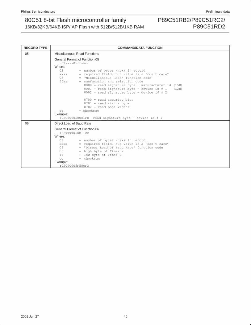
Philips Semiconductors Preliminary data
P89C51RB2/P89C51RC2/P89C51RD2
80C51 8-bit Flash microcontroller family16KB/32KB/64KB ISP/IAP Flash with 512B/512B/1KB RAM
2001 Jun 27 45
RECORD TYPE COMMAND/DATA FUNCTION
05 Miscellaneous Read Functions
General Format of Function 05:02xxxx05ffsscc
Where:02 = number of bytes (hex) in recordxxxx = required field, but value is a “don’t care”05 = “Miscellaneous Read” function codeffss = subfunction and selection code
0000 = read signature byte – manufacturer id (15H)0001 = read signature byte – device id # 1 (C2H)0002 = read signature byte – device id # 2
0700 = read security bits0701 = read status byte0702 = read boot vector
cc = checksumExample:
:020000050001F8 read signature byte – device id # 1
06 Direct Load of Baud Rate
General Format of Function 06:02xxxx06hhllcc
Where:02 = number of bytes (hex) in recordxxxx = required field, but value is a “don’t care”06 = ”Direct Load of Baud Rate” function codehh = high byte of Timer 2ll = low byte of Timer 2cc = checksum
Example::02000006F500F3
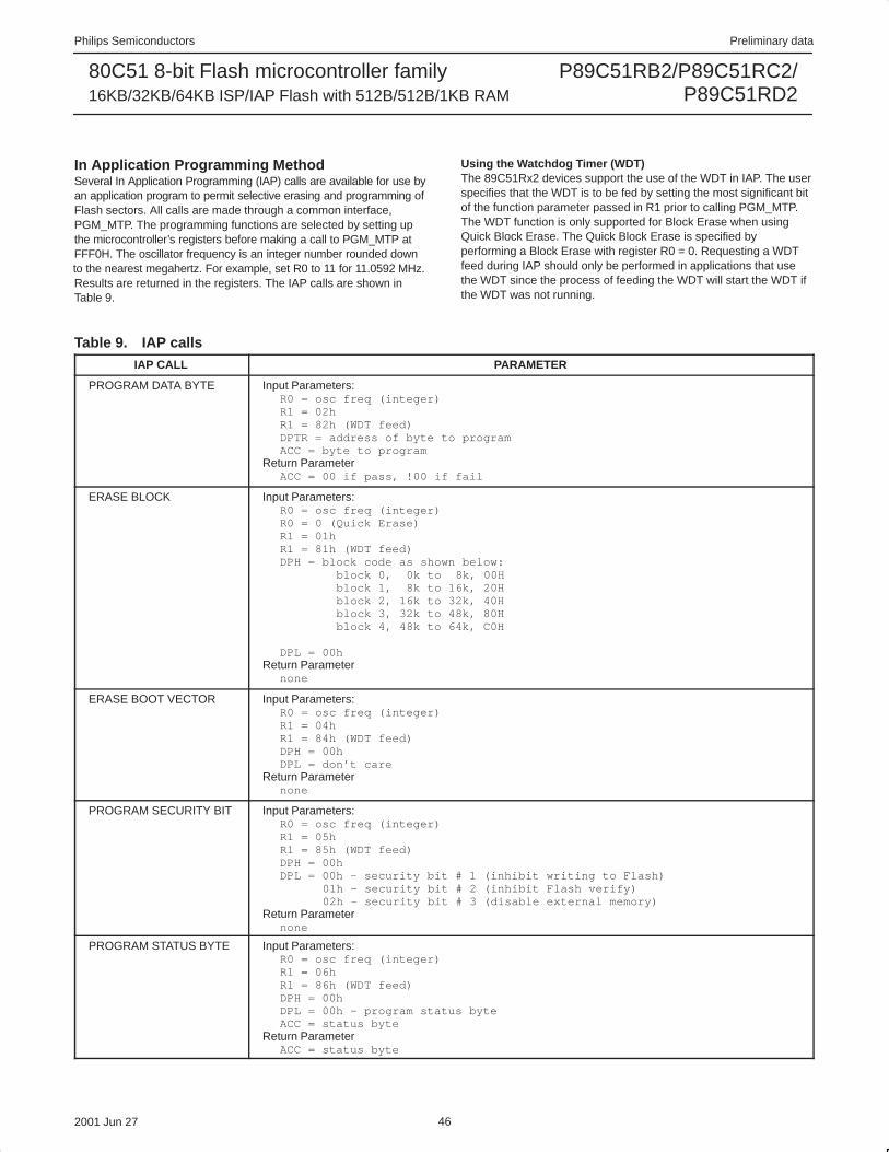
Philips Semiconductors Preliminary data
P89C51RB2/P89C51RC2/P89C51RD2
80C51 8-bit Flash microcontroller family16KB/32KB/64KB ISP/IAP Flash with 512B/512B/1KB RAM
2001 Jun 27 46
In Application Programming MethodSeveral In Application Programming (IAP) calls are available for use byan application program to permit selective erasing and programming ofFlash sectors. All calls are made through a common interface,PGM_MTP. The programming functions are selected by setting upthe microcontroller’s registers before making a call to PGM_MTP atFFF0H. The oscillator frequency is an integer number rounded downto the nearest megahertz. For example, set R0 to 11 for 11.0592 MHz.Results are returned in the registers. The IAP calls are shown inTable 9.
Using the Watchdog Timer (WDT)The 89C51Rx2 devices support the use of the WDT in IAP. The userspecifies that the WDT is to be fed by setting the most significant bitof the function parameter passed in R1 prior to calling PGM_MTP.The WDT function is only supported for Block Erase when usingQuick Block Erase. The Quick Block Erase is specified byperforming a Block Erase with register R0 = 0. Requesting a WDTfeed during IAP should only be performed in applications that usethe WDT since the process of feeding the WDT will start the WDT ifthe WDT was not running.
Table 9. IAP callsIAP CALL PARAMETER
PROGRAM DATA BYTE Input Parameters:R0 = osc freq (integer)R1 = 02hR1 = 82h (WDT feed)DPTR = address of byte to programACC = byte to program
Return ParameterACC = 00 if pass, !00 if fail
ERASE BLOCK Input Parameters:R0 = osc freq (integer)R0 = 0 (Quick Erase)R1 = 01hR1 = 81h (WDT feed)DPH = block code as shown below: block 0, 0k to 8k, 00H block 1, 8k to 16k, 20H block 2, 16k to 32k, 40H block 3, 32k to 48k, 80H block 4, 48k to 64k, C0H
DPL = 00hReturn Parameter
none
ERASE BOOT VECTOR Input Parameters:R0 = osc freq (integer)R1 = 04hR1 = 84h (WDT feed)DPH = 00hDPL = don’t care
Return Parameternone
PROGRAM SECURITY BIT Input Parameters:R0 = osc freq (integer)R1 = 05hR1 = 85h (WDT feed)DPH = 00hDPL = 00h – security bit # 1 (inhibit writing to Flash) 01h – security bit # 2 (inhibit Flash verify) 02h – security bit # 3 (disable external memory)
Return Parameternone
PROGRAM STATUS BYTE Input Parameters:R0 = osc freq (integer)R1 = 06hR1 = 86h (WDT feed)DPH = 00hDPL = 00h – program status byteACC = status byte
Return ParameterACC = status byte
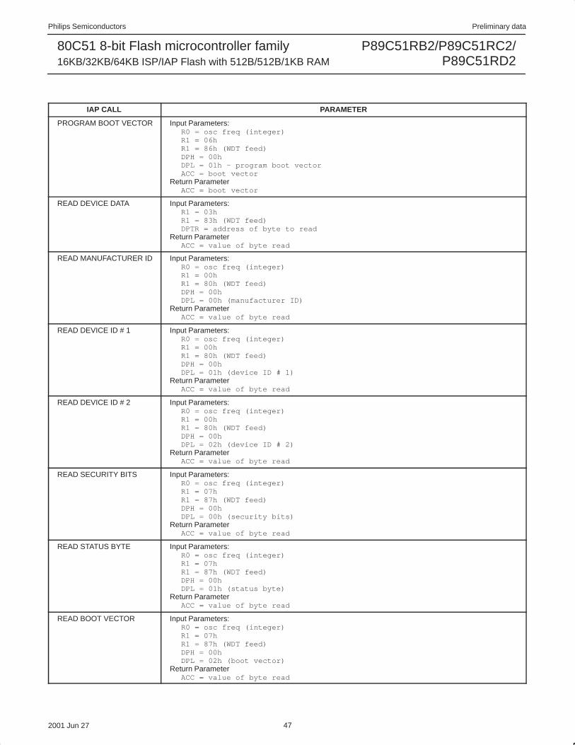
Philips Semiconductors Preliminary data
P89C51RB2/P89C51RC2/P89C51RD2
80C51 8-bit Flash microcontroller family16KB/32KB/64KB ISP/IAP Flash with 512B/512B/1KB RAM
2001 Jun 27 47
IAP CALL PARAMETER
PROGRAM BOOT VECTOR Input Parameters:R0 = osc freq (integer)R1 = 06hR1 = 86h (WDT feed)DPH = 00hDPL = 01h – program boot vectorACC = boot vector
Return ParameterACC = boot vector
READ DEVICE DATA Input Parameters:R1 = 03hR1 = 83h (WDT feed)DPTR = address of byte to read
Return ParameterACC = value of byte read
READ MANUFACTURER ID Input Parameters:R0 = osc freq (integer)R1 = 00hR1 = 80h (WDT feed)DPH = 00hDPL = 00h (manufacturer ID)
Return ParameterACC = value of byte read
READ DEVICE ID # 1 Input Parameters:R0 = osc freq (integer)R1 = 00hR1 = 80h (WDT feed)DPH = 00hDPL = 01h (device ID # 1)
Return ParameterACC = value of byte read
READ DEVICE ID # 2 Input Parameters:R0 = osc freq (integer)R1 = 00hR1 = 80h (WDT feed)DPH = 00hDPL = 02h (device ID # 2)
Return ParameterACC = value of byte read
READ SECURITY BITS Input Parameters:R0 = osc freq (integer)R1 = 07hR1 = 87h (WDT feed)DPH = 00hDPL = 00h (security bits)
Return ParameterACC = value of byte read
READ STATUS BYTE Input Parameters:R0 = osc freq (integer)R1 = 07hR1 = 87h (WDT feed)DPH = 00hDPL = 01h (status byte)
Return ParameterACC = value of byte read
READ BOOT VECTOR Input Parameters:R0 = osc freq (integer)R1 = 07hR1 = 87h (WDT feed)DPH = 00hDPL = 02h (boot vector)
Return ParameterACC = value of byte read
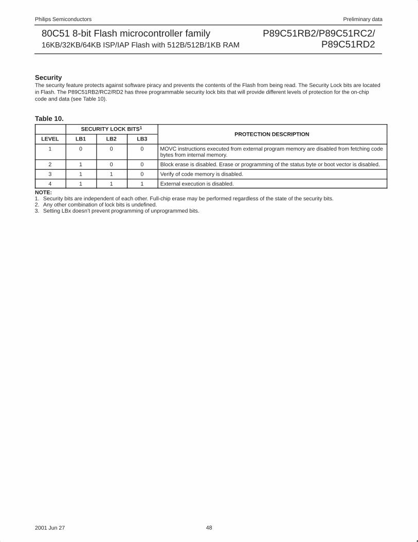
Philips Semiconductors Preliminary data
P89C51RB2/P89C51RC2/P89C51RD2
80C51 8-bit Flash microcontroller family16KB/32KB/64KB ISP/IAP Flash with 512B/512B/1KB RAM
2001 Jun 27 48
SecurityThe security feature protects against software piracy and prevents the contents of the Flash from being read. The Security Lock bits are locatedin Flash. The P89C51RB2/RC2/RD2 has three programmable security lock bits that will provide different levels of protection for the on-chipcode and data (see Table 10).
Table 10.SECURITY LOCK BITS 1
PROTECTION DESCRIPTIONLEVEL LB1 LB2 LB3
PROTECTION DESCRIPTION
1 0 0 0 MOVC instructions executed from external program memory are disabled from fetching codebytes from internal memory.
2 1 0 0 Block erase is disabled. Erase or programming of the status byte or boot vector is disabled.
3 1 1 0 Verify of code memory is disabled.
4 1 1 1 External execution is disabled.
NOTE:1. Security bits are independent of each other. Full-chip erase may be performed regardless of the state of the security bits.2. Any other combination of lock bits is undefined.3. Setting LBx doesn’t prevent programming of unprogrammed bits.
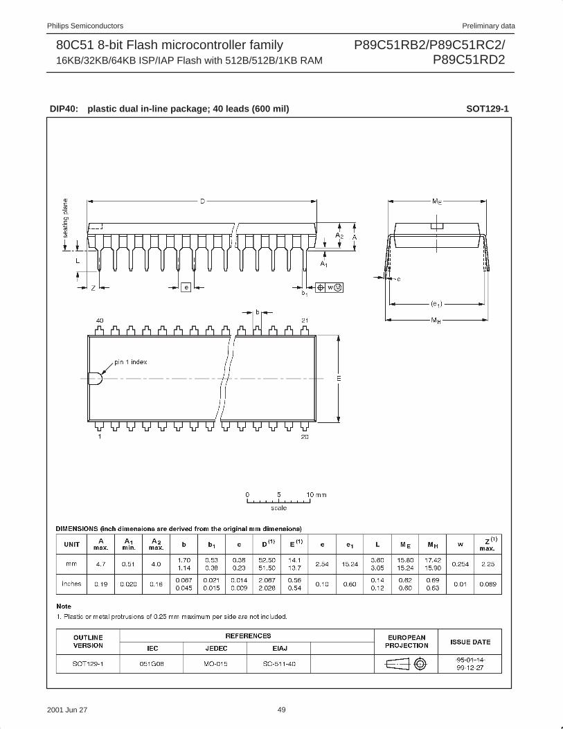
Philips Semiconductors Preliminary data
P89C51RB2/P89C51RC2/P89C51RD2
80C51 8-bit Flash microcontroller family16KB/32KB/64KB ISP/IAP Flash with 512B/512B/1KB RAM
2001 Jun 27 49
DIP40: plastic dual in-line package; 40 leads (600 mil) SOT129-1
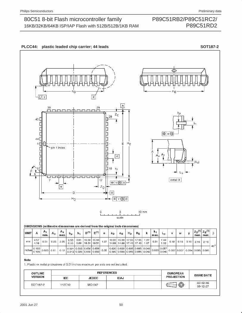
Philips Semiconductors Preliminary data
P89C51RB2/P89C51RC2/P89C51RD2
80C51 8-bit Flash microcontroller family16KB/32KB/64KB ISP/IAP Flash with 512B/512B/1KB RAM
2001 Jun 27 50
PLCC44: plastic leaded chip carrier; 44 leads SOT187-2
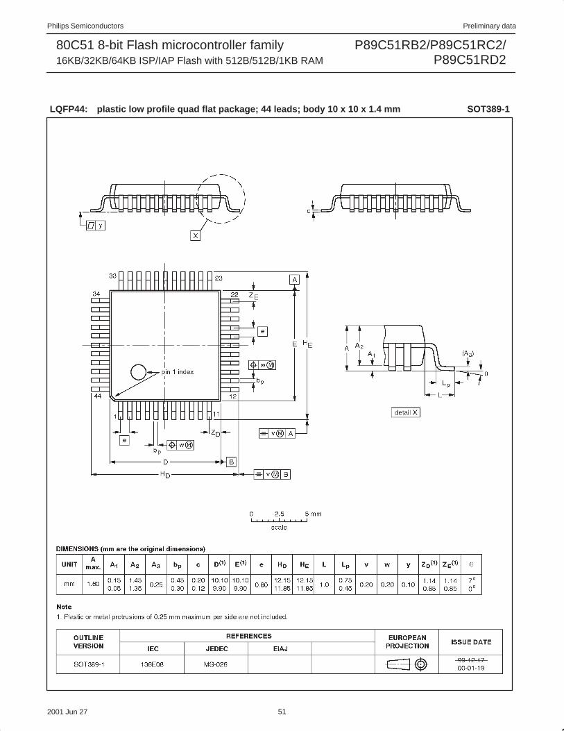
Philips Semiconductors Preliminary data
P89C51RB2/P89C51RC2/P89C51RD2
80C51 8-bit Flash microcontroller family16KB/32KB/64KB ISP/IAP Flash with 512B/512B/1KB RAM
2001 Jun 27 51
LQFP44: plastic low profile quad flat package; 44 leads; body 10 x 10 x 1.4 mm SOT389-1
Philips Semiconductors Preliminary data
P89C51RB2/P89C51RC2/P89C51RD2
80C51 8-bit Flash microcontroller family16KB/32KB/64KB ISP/IAP Flash with 512B/512B/1KB RAM
2001 Jun 27 52
DefinitionsShort-form specification — The data in a short-form specification is extracted from a full data sheet with the same type number and title. Fordetailed information see the relevant data sheet or data handbook.
Limiting values definition — Limiting values given are in accordance with the Absolute Maximum Rating System (IEC 60134). Stress above oneor more of the limiting values may cause permanent damage to the device. These are stress ratings only and operation of the device at these orat any other conditions above those given in the Characteristics sections of the specification is not implied. Exposure to limiting values for extendedperiods may affect device reliability.
Application information — Applications that are described herein for any of these products are for illustrative purposes only. PhilipsSemiconductors make no representation or warranty that such applications will be suitable for the specified use without further testing ormodification.
DisclaimersLife support — These products are not designed for use in life support appliances, devices or systems where malfunction of these products canreasonably be expected to result in personal injury. Philips Semiconductors customers using or selling these products for use in such applicationsdo so at their own risk and agree to fully indemnify Philips Semiconductors for any damages resulting from such application.
Right to make changes — Philips Semiconductors reserves the right to make changes, without notice, in the products, including circuits, standardcells, and/or software, described or contained herein in order to improve design and/or performance. Philips Semiconductors assumes noresponsibility or liability for the use of any of these products, conveys no license or title under any patent, copyright, or mask work right to theseproducts, and makes no representations or warranties that these products are free from patent, copyright, or mask work right infringement, unlessotherwise specified.
Philips Semiconductors811 East Arques AvenueP.O. Box 3409Sunnyvale, California 94088–3409Telephone 800-234-7381
Copyright Philips Electronics North America Corporation 2001All rights reserved. Printed in U.S.A.
Date of release: 06-01
Document order number: 9397 750 08525
������ ����������
Data sheet status [1]
Objective data
Preliminary data
Product data
Productstatus [2]
Development
Qualification
Production
Definitions
This data sheet contains data from the objective specification for product development.Philips Semiconductors reserves the right to change the specification in any manner without notice.
This data sheet contains data from the preliminary specification. Supplementary data will bepublished at a later date. Philips Semiconductors reserves the right to change the specificationwithout notice, in order to improve the design and supply the best possible product.
This data sheet contains data from the product specification. Philips Semiconductors reserves theright to make changes at any time in order to improve the design, manufacturing and supply.Changes will be communicated according to the Customer Product/Process Change Notification(CPCN) procedure SNW-SQ-650A.
Data sheet status
[1] Please consult the most recently issued data sheet before initiating or completing a design.
[2] The product status of the device(s) described in this data sheet may have changed since this data sheet was published. The latest information is available on the Internet at URLhttp://www.semiconductors.philips.com.