P5Q Serial Phase Change Memory (PCM) - Xilinx · READ IDENTIFICATION ... with data retention...
46
Products and specifications discussed herein are subject to change by Micron without notice. 32Mb, 64Mb, 128Mb: P5Q Serial PCM Features PDF: 09005aef8447d377/Source: 09005aef845b5cb5 Micron Technology, Inc., reserves the right to change products or specifications without notice. p5q_32_64_128Mb_serial_pcm_1.fm - Rev. G 1/12 EN 1 ©2005 Micron Technology, Inc. All rights reserved. P5Q Serial Phase Change Memory (PCM) NP5Q032AE3ESFC0E, NP5Q064AE3ESFC0E NP5Q128A13ESFC0E, NP5Q128AE3ESFC0E Features • Density range: 32Mb, 64Mb, 128Mb • SPI bus compatible serial interface • Maximum clock frequency – 66 MHz (0°C to +70°C) – 33 MHz (–40°C to +85°C) • 2.7V to 3.6V single supply voltage • Supports legacy SPI protocol and new quad I/O or dual I/O SPI protocol • Quad I/O frequency of 50 MHz, resulting in an equivalent clock frequency up to 200 MHz • Dual I/O frequency of 66 MHz, resulting in an equivalent clock frequency up to 132 MHz • Continuous READ of entire memory via single instruction: – Quad and dual output fast read – Quad and dual input fast program • Uniform 128KB sectors (Flash emulation) • WRITE operations – 128KB sectors ERASE (emulated) – Legacy Flash PAGE PROGRAM – Bit-alterable page WRITEs – PAGE PROGRAM on all 1s (PRESET WRITEs) • Write protections: protected area size defined by four nonvolatile bits (BP0, BP1, BP2, and BP3) • JEDEC-standard two-byte signature – 32Mb (DA16h) – 64Mb (DA17h) – 128Mb (DA18h) • 32M, 64Mb, and 128Mb densities with SOIC16 package • More than 1,000,000 WRITE cycles • Phase change memory (PCM) – Chalcogenide phase change storage element – Bit-alterable WRITE operation
-
Upload
truongnguyet -
Category
Documents
-
view
224 -
download
1
Transcript of P5Q Serial Phase Change Memory (PCM) - Xilinx · READ IDENTIFICATION ... with data retention...

32Mb, 64Mb, 128Mb: P5Q Serial PCMFeatures
P5Q Serial Phase Change Memory (PCM)NP5Q032AE3ESFC0E, NP5Q064AE3ESFC0ENP5Q128A13ESFC0E, NP5Q128AE3ESFC0E
Features• Density range: 32Mb, 64Mb, 128Mb• SPI bus compatible serial interface• Maximum clock frequency
– 66 MHz (0°C to +70°C)– 33 MHz (–40°C to +85°C)
• 2.7V to 3.6V single supply voltage• Supports legacy SPI protocol and new quad I/O or
dual I/O SPI protocol• Quad I/O frequency of 50 MHz, resulting in an
equivalent clock frequency up to 200 MHz• Dual I/O frequency of 66 MHz, resulting in an
equivalent clock frequency up to 132 MHz• Continuous READ of entire memory via single
instruction:– Quad and dual output fast read– Quad and dual input fast program
• Uniform 128KB sectors (Flash emulation)• WRITE operations
– 128KB sectors ERASE (emulated)– Legacy Flash PAGE PROGRAM– Bit-alterable page WRITEs – PAGE PROGRAM on all 1s (PRESET WRITEs)
• Write protections: protected area size defined by four nonvolatile bits (BP0, BP1, BP2, and BP3)
• JEDEC-standard two-byte signature– 32Mb (DA16h)– 64Mb (DA17h)– 128Mb (DA18h)
• 32M, 64Mb, and 128Mb densities with SOIC16 package
• More than 1,000,000 WRITE cycles • Phase change memory (PCM)
– Chalcogenide phase change storage element– Bit-alterable WRITE operation
Products and specifications discussed herein are
PDF: 09005aef8447d377/Source: 09005aef845b5cb5p5q_32_64_128Mb_serial_pcm_1.fm - Rev. G 1/12 EN 1
subject to change by Micron without notice.
Micron Technology, Inc., reserves the right to change products or specifications without notice.©2005 Micron Technology, Inc. All rights reserved.

32Mb, 64Mb, 128Mb: P5Q Serial PCMTable of Contents
Table of ContentsFeatures . . . . . . . . . . . . . . . . . . . . . . . . . . . . . . . . . . . . . . . . . . . . . . . . . . . . . . . . . . . . . . . . . . . . . . . . . . . . . . . . . . . . . . . . . . . . . .1Functional Description . . . . . . . . . . . . . . . . . . . . . . . . . . . . . . . . . . . . . . . . . . . . . . . . . . . . . . . . . . . . . . . . . . . . . . . . . . . . . . . .6Product Features . . . . . . . . . . . . . . . . . . . . . . . . . . . . . . . . . . . . . . . . . . . . . . . . . . . . . . . . . . . . . . . . . . . . . . . . . . . . . . . . . . . . . .6Signal Names . . . . . . . . . . . . . . . . . . . . . . . . . . . . . . . . . . . . . . . . . . . . . . . . . . . . . . . . . . . . . . . . . . . . . . . . . . . . . . . . . . . . . . . . .8Signal Descriptions . . . . . . . . . . . . . . . . . . . . . . . . . . . . . . . . . . . . . . . . . . . . . . . . . . . . . . . . . . . . . . . . . . . . . . . . . . . . . . . . . . . .8
Serial Data Input (D/DQ0) . . . . . . . . . . . . . . . . . . . . . . . . . . . . . . . . . . . . . . . . . . . . . . . . . . . . . . . . . . . . . . . . . . . . . . . . . . .8Serial Data Output (Q/DQ1) . . . . . . . . . . . . . . . . . . . . . . . . . . . . . . . . . . . . . . . . . . . . . . . . . . . . . . . . . . . . . . . . . . . . . . . . .8Serial Clock (C) . . . . . . . . . . . . . . . . . . . . . . . . . . . . . . . . . . . . . . . . . . . . . . . . . . . . . . . . . . . . . . . . . . . . . . . . . . . . . . . . . . . . .8Chip Select (S#) . . . . . . . . . . . . . . . . . . . . . . . . . . . . . . . . . . . . . . . . . . . . . . . . . . . . . . . . . . . . . . . . . . . . . . . . . . . . . . . . . . . . .9Hold (HOLD#/DQ3). . . . . . . . . . . . . . . . . . . . . . . . . . . . . . . . . . . . . . . . . . . . . . . . . . . . . . . . . . . . . . . . . . . . . . . . . . . . . . . . .9Write Protect (W#/DQ2) . . . . . . . . . . . . . . . . . . . . . . . . . . . . . . . . . . . . . . . . . . . . . . . . . . . . . . . . . . . . . . . . . . . . . . . . . . . . .9VCC Supply Voltage . . . . . . . . . . . . . . . . . . . . . . . . . . . . . . . . . . . . . . . . . . . . . . . . . . . . . . . . . . . . . . . . . . . . . . . . . . . . . . . . .9VSS Ground . . . . . . . . . . . . . . . . . . . . . . . . . . . . . . . . . . . . . . . . . . . . . . . . . . . . . . . . . . . . . . . . . . . . . . . . . . . . . . . . . . . . . . . .9
SPI Modes . . . . . . . . . . . . . . . . . . . . . . . . . . . . . . . . . . . . . . . . . . . . . . . . . . . . . . . . . . . . . . . . . . . . . . . . . . . . . . . . . . . . . . . . . . . .9Operating Features . . . . . . . . . . . . . . . . . . . . . . . . . . . . . . . . . . . . . . . . . . . . . . . . . . . . . . . . . . . . . . . . . . . . . . . . . . . . . . . . . . .12
PAGE PROGRAM . . . . . . . . . . . . . . . . . . . . . . . . . . . . . . . . . . . . . . . . . . . . . . . . . . . . . . . . . . . . . . . . . . . . . . . . . . . . . . . . . .12DUAL INPUT FAST PROGRAM . . . . . . . . . . . . . . . . . . . . . . . . . . . . . . . . . . . . . . . . . . . . . . . . . . . . . . . . . . . . . . . . . . . . . .12QUAD INPUT FAST PROGRAM . . . . . . . . . . . . . . . . . . . . . . . . . . . . . . . . . . . . . . . . . . . . . . . . . . . . . . . . . . . . . . . . . . . . .12SECTOR ERASE and BULK ERASE . . . . . . . . . . . . . . . . . . . . . . . . . . . . . . . . . . . . . . . . . . . . . . . . . . . . . . . . . . . . . . . . . . .12Polling During a WRITE, PROGRAM, or ERASE Cycle . . . . . . . . . . . . . . . . . . . . . . . . . . . . . . . . . . . . . . . . . . . . . . . . . .13Active Power and Standby Power . . . . . . . . . . . . . . . . . . . . . . . . . . . . . . . . . . . . . . . . . . . . . . . . . . . . . . . . . . . . . . . . . . . .13Status Register. . . . . . . . . . . . . . . . . . . . . . . . . . . . . . . . . . . . . . . . . . . . . . . . . . . . . . . . . . . . . . . . . . . . . . . . . . . . . . . . . . . . .13Protocol-Related Protections. . . . . . . . . . . . . . . . . . . . . . . . . . . . . . . . . . . . . . . . . . . . . . . . . . . . . . . . . . . . . . . . . . . . . . . .13Hold Condition . . . . . . . . . . . . . . . . . . . . . . . . . . . . . . . . . . . . . . . . . . . . . . . . . . . . . . . . . . . . . . . . . . . . . . . . . . . . . . . . . . . .14
Memory Organization . . . . . . . . . . . . . . . . . . . . . . . . . . . . . . . . . . . . . . . . . . . . . . . . . . . . . . . . . . . . . . . . . . . . . . . . . . . . . . . .15Instructions . . . . . . . . . . . . . . . . . . . . . . . . . . . . . . . . . . . . . . . . . . . . . . . . . . . . . . . . . . . . . . . . . . . . . . . . . . . . . . . . . . . . . . . . .17
WRITE ENABLE (WREN). . . . . . . . . . . . . . . . . . . . . . . . . . . . . . . . . . . . . . . . . . . . . . . . . . . . . . . . . . . . . . . . . . . . . . . . . . . .18WRITE DISABLE (WRDI). . . . . . . . . . . . . . . . . . . . . . . . . . . . . . . . . . . . . . . . . . . . . . . . . . . . . . . . . . . . . . . . . . . . . . . . . . . .18READ IDENTIFICATION (RDID) . . . . . . . . . . . . . . . . . . . . . . . . . . . . . . . . . . . . . . . . . . . . . . . . . . . . . . . . . . . . . . . . . . . .19READ STATUS REGISTER (RDSR) . . . . . . . . . . . . . . . . . . . . . . . . . . . . . . . . . . . . . . . . . . . . . . . . . . . . . . . . . . . . . . . . . . .20WRITE STATUS REGISTER (WRSR) . . . . . . . . . . . . . . . . . . . . . . . . . . . . . . . . . . . . . . . . . . . . . . . . . . . . . . . . . . . . . . . . . .21Read Data Bytes (READ) . . . . . . . . . . . . . . . . . . . . . . . . . . . . . . . . . . . . . . . . . . . . . . . . . . . . . . . . . . . . . . . . . . . . . . . . . . . .23Read Data Bytes at Higher Speed (FAST_READ) . . . . . . . . . . . . . . . . . . . . . . . . . . . . . . . . . . . . . . . . . . . . . . . . . . . . . . .24DUAL OUTPUT FAST READ (DOFR) . . . . . . . . . . . . . . . . . . . . . . . . . . . . . . . . . . . . . . . . . . . . . . . . . . . . . . . . . . . . . . . . .25QUAD OUTPUT FAST READ (QOFR) . . . . . . . . . . . . . . . . . . . . . . . . . . . . . . . . . . . . . . . . . . . . . . . . . . . . . . . . . . . . . . . .26PAGE PROGRAM (PP) . . . . . . . . . . . . . . . . . . . . . . . . . . . . . . . . . . . . . . . . . . . . . . . . . . . . . . . . . . . . . . . . . . . . . . . . . . . . . .27DUAL INPUT FAST PROGRAM (DIFP) . . . . . . . . . . . . . . . . . . . . . . . . . . . . . . . . . . . . . . . . . . . . . . . . . . . . . . . . . . . . . . .28QUAD INPUT FAST PROGRAM (QIFP) . . . . . . . . . . . . . . . . . . . . . . . . . . . . . . . . . . . . . . . . . . . . . . . . . . . . . . . . . . . . . . .29SECTOR ERASE (SE) . . . . . . . . . . . . . . . . . . . . . . . . . . . . . . . . . . . . . . . . . . . . . . . . . . . . . . . . . . . . . . . . . . . . . . . . . . . . . . .31BULK ERASE (BE) . . . . . . . . . . . . . . . . . . . . . . . . . . . . . . . . . . . . . . . . . . . . . . . . . . . . . . . . . . . . . . . . . . . . . . . . . . . . . . . . . .31
Power-Up and Power-Down. . . . . . . . . . . . . . . . . . . . . . . . . . . . . . . . . . . . . . . . . . . . . . . . . . . . . . . . . . . . . . . . . . . . . . . . . . .32Initial Delivery State . . . . . . . . . . . . . . . . . . . . . . . . . . . . . . . . . . . . . . . . . . . . . . . . . . . . . . . . . . . . . . . . . . . . . . . . . . . . . . . . . .33Maximum Ratings . . . . . . . . . . . . . . . . . . . . . . . . . . . . . . . . . . . . . . . . . . . . . . . . . . . . . . . . . . . . . . . . . . . . . . . . . . . . . . . . . . . .34DC and AC Characteristics . . . . . . . . . . . . . . . . . . . . . . . . . . . . . . . . . . . . . . . . . . . . . . . . . . . . . . . . . . . . . . . . . . . . . . . . . . . .34
Operating Conditions . . . . . . . . . . . . . . . . . . . . . . . . . . . . . . . . . . . . . . . . . . . . . . . . . . . . . . . . . . . . . . . . . . . . . . . . . . . . . .34Endurance Specifications. . . . . . . . . . . . . . . . . . . . . . . . . . . . . . . . . . . . . . . . . . . . . . . . . . . . . . . . . . . . . . . . . . . . . . . . . . .34AC Measurement Conditions . . . . . . . . . . . . . . . . . . . . . . . . . . . . . . . . . . . . . . . . . . . . . . . . . . . . . . . . . . . . . . . . . . . . . . .35Capacitance . . . . . . . . . . . . . . . . . . . . . . . . . . . . . . . . . . . . . . . . . . . . . . . . . . . . . . . . . . . . . . . . . . . . . . . . . . . . . . . . . . . . . . .36DC Characteristics . . . . . . . . . . . . . . . . . . . . . . . . . . . . . . . . . . . . . . . . . . . . . . . . . . . . . . . . . . . . . . . . . . . . . . . . . . . . . . . . .36AC Characteristics . . . . . . . . . . . . . . . . . . . . . . . . . . . . . . . . . . . . . . . . . . . . . . . . . . . . . . . . . . . . . . . . . . . . . . . . . . . . . . . . .37
Package Dimensions . . . . . . . . . . . . . . . . . . . . . . . . . . . . . . . . . . . . . . . . . . . . . . . . . . . . . . . . . . . . . . . . . . . . . . . . . . . . . . . . .40
PDF: 09005aef8447d377/Source: 09005aef845b5cb5 Micron Technology, Inc., reserves the right to change products or specifications without notice.p5q_32_64_128Mb_serial_pcm_TOC.fm - Rev. G 1/12 EN 2 ©2005 Micron Technology, Inc. All rights reserved.

32Mb, 64Mb, 128Mb: P5Q Serial PCMTable of Contents
Ordering Information. . . . . . . . . . . . . . . . . . . . . . . . . . . . . . . . . . . . . . . . . . . . . . . . . . . . . . . . . . . . . . . . . . . . . . . . . . . . . . . . .41
PDF: 09005aef8447d377/Source: 09005aef845b5cb5 Micron Technology, Inc., reserves the right to change products or specifications without notice.p5q_32_64_128Mb_serial_pcm_TOC.fm - Rev. G 1/12 EN 3 ©2005 Micron Technology, Inc. All rights reserved.
PDF: 09005aef8447d377/Source: 09005aef845b5cb5 Micron Technology, Inc., reserves the right to change products or specifications without notice.p5q_32_64_128Mb_serial_pcm_LOT.fm - Rev. G 1/12 EN 4 ©2005 Micron Technology, Inc. All rights reserved.
32Mb, 64Mb, 128Mb: P5Q Serial PCMList of Tables
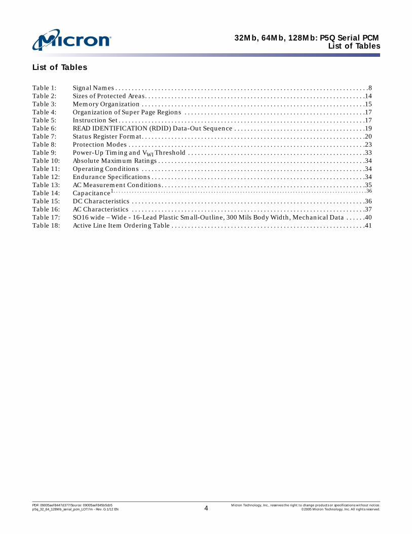
List of Tables
Table 1: Signal Names . . . . . . . . . . . . . . . . . . . . . . . . . . . . . . . . . . . . . . . . . . . . . . . . . . . . . . . . . . . . . . . . . . . . . . . . . . . . .8Table 2: Sizes of Protected Areas. . . . . . . . . . . . . . . . . . . . . . . . . . . . . . . . . . . . . . . . . . . . . . . . . . . . . . . . . . . . . . . . . . .14Table 3: Memory Organization . . . . . . . . . . . . . . . . . . . . . . . . . . . . . . . . . . . . . . . . . . . . . . . . . . . . . . . . . . . . . . . . . . . .15Table 4: Organization of Super Page Regions . . . . . . . . . . . . . . . . . . . . . . . . . . . . . . . . . . . . . . . . . . . . . . . . . . . . . . .17Table 5: Instruction Set . . . . . . . . . . . . . . . . . . . . . . . . . . . . . . . . . . . . . . . . . . . . . . . . . . . . . . . . . . . . . . . . . . . . . . . . . . .17Table 6: READ IDENTIFICATION (RDID) Data-Out Sequence . . . . . . . . . . . . . . . . . . . . . . . . . . . . . . . . . . . . . . . .19Table 7: Status Register Format. . . . . . . . . . . . . . . . . . . . . . . . . . . . . . . . . . . . . . . . . . . . . . . . . . . . . . . . . . . . . . . . . . . .20Table 8: Protection Modes . . . . . . . . . . . . . . . . . . . . . . . . . . . . . . . . . . . . . . . . . . . . . . . . . . . . . . . . . . . . . . . . . . . . . . . .23Table 9: Power-Up Timing and VWI Threshold . . . . . . . . . . . . . . . . . . . . . . . . . . . . . . . . . . . . . . . . . . . . . . . . . . . . . .33Table 10: Absolute Maximum Ratings . . . . . . . . . . . . . . . . . . . . . . . . . . . . . . . . . . . . . . . . . . . . . . . . . . . . . . . . . . . . . . .34Table 11: Operating Conditions . . . . . . . . . . . . . . . . . . . . . . . . . . . . . . . . . . . . . . . . . . . . . . . . . . . . . . . . . . . . . . . . . . . .34Table 12: Endurance Specifications . . . . . . . . . . . . . . . . . . . . . . . . . . . . . . . . . . . . . . . . . . . . . . . . . . . . . . . . . . . . . . . . .34Table 13: AC Measurement Conditions. . . . . . . . . . . . . . . . . . . . . . . . . . . . . . . . . . . . . . . . . . . . . . . . . . . . . . . . . . . . . .35Table 14: Capacitance1. . . . . . . . . . . . . . . . . . . . . . . . . . . . . . . . . . . . . . . . . . . . . . . . . . . . . . . . . . . . . . . . . . . . . . . . . . . . . . . . . . . . . . . . . . . . . . . .36
Table 15: DC Characteristics . . . . . . . . . . . . . . . . . . . . . . . . . . . . . . . . . . . . . . . . . . . . . . . . . . . . . . . . . . . . . . . . . . . . . . .36Table 16: AC Characteristics . . . . . . . . . . . . . . . . . . . . . . . . . . . . . . . . . . . . . . . . . . . . . . . . . . . . . . . . . . . . . . . . . . . . . . .37Table 17: SO16 wide – Wide - 16-Lead Plastic Small-Outline, 300 Mils Body Width, Mechanical Data . . . . . .40Table 18: Active Line Item Ordering Table . . . . . . . . . . . . . . . . . . . . . . . . . . . . . . . . . . . . . . . . . . . . . . . . . . . . . . . . . . .41

PDF: 09005aef8447d377/Source: 09005aef845b5cb5 Micron Technology, Inc., reserves the right to change products or specifications without notice.p5q_32_64_128Mb_serial_pcm_LOF.fm - Rev. G 1/12 EN 5 ©2005 Micron Technology, Inc. All rights reserved.
32Mb, 64Mb, 128Mb: P5Q Serial PCMList of Figures
List of FiguresFigure 1: Logic Diagram . . . . . . . . . . . . . . . . . . . . . . . . . . . . . . . . . . . . . . . . . . . . . . . . . . . . . . . . . . . . . . . . . . . . . . . . . . . .7Figure 2: SO16 Connections . . . . . . . . . . . . . . . . . . . . . . . . . . . . . . . . . . . . . . . . . . . . . . . . . . . . . . . . . . . . . . . . . . . . . . . .7Figure 3: Bus Master and Memory Devices on the SPI Bus . . . . . . . . . . . . . . . . . . . . . . . . . . . . . . . . . . . . . . . . . . . .10Figure 4: SPI Modes Supported . . . . . . . . . . . . . . . . . . . . . . . . . . . . . . . . . . . . . . . . . . . . . . . . . . . . . . . . . . . . . . . . . . . .11Figure 5: Hold Condition Activation . . . . . . . . . . . . . . . . . . . . . . . . . . . . . . . . . . . . . . . . . . . . . . . . . . . . . . . . . . . . . . . .15Figure 6: WRITE ENABLE (WREN) Instruction Sequence. . . . . . . . . . . . . . . . . . . . . . . . . . . . . . . . . . . . . . . . . . . . . .18Figure 7: WRITE DISABLE (WRDI) Instruction Sequence . . . . . . . . . . . . . . . . . . . . . . . . . . . . . . . . . . . . . . . . . . . . .19Figure 8: READ IDENTIFICATION (RDID) Instruction Sequence and Data-Out Sequence . . . . . . . . . . . . . . . .20Figure 9: READ STATUS REGISTER (RDSR) Instruction Sequence and Data-Out Sequence. . . . . . . . . . . . . . .21Figure 10: WRITE STATUS REGISTER (WRSR) Instruction Sequence . . . . . . . . . . . . . . . . . . . . . . . . . . . . . . . . . . . .22Figure 11: READ DATA BYTES (READ) Instruction Sequence and Data-Out Sequence . . . . . . . . . . . . . . . . . . . .24Figure 12: FAST_READ Instruction Sequence . . . . . . . . . . . . . . . . . . . . . . . . . . . . . . . . . and Data-Out Sequence25Figure 13: DUAL OUTPUT FAST READ Instruction Sequence . . . . . . . . . . . . . . . . . . . . . . . . . . . . . . . . . . . . . . . . . .26Figure 14: QUAD OUTPUT FAST READ Instruction Sequence . . . . . . . . . . . . . . . . . . . . . . . . . . . . . . . . . . . . . . . . . .27Figure 15: PP Instruction Sequence . . . . . . . . . . . . . . . . . . . . . . . . . . . . . . . . . . . . . . . . . . . . . . . . . . . . . . . . . . . . . . . . . .28Figure 16: DIFP Instruction Sequence. . . . . . . . . . . . . . . . . . . . . . . . . . . . . . . . . . . . . . . . . . . . . . . . . . . . . . . . . . . . . . . .29Figure 17: QIFP Instruction Sequence. . . . . . . . . . . . . . . . . . . . . . . . . . . . . . . . . . . . . . . . . . . . . . . . . . . . . . . . . . . . . . . .30Figure 18: SE Instruction Sequence . . . . . . . . . . . . . . . . . . . . . . . . . . . . . . . . . . . . . . . . . . . . . . . . . . . . . . . . . . . . . . . . . .31Figure 19: BE Instruction Sequence. . . . . . . . . . . . . . . . . . . . . . . . . . . . . . . . . . . . . . . . . . . . . . . . . . . . . . . . . . . . . . . . . .32Figure 20: Power-Up Timing . . . . . . . . . . . . . . . . . . . . . . . . . . . . . . . . . . . . . . . . . . . . . . . . . . . . . . . . . . . . . . . . . . . . . . . .33Figure 21: AC Measurement I/O Waveform. . . . . . . . . . . . . . . . . . . . . . . . . . . . . . . . . . . . . . . . . . . . . . . . . . . . . . . . . . .35Figure 22: Serial Input Timing. . . . . . . . . . . . . . . . . . . . . . . . . . . . . . . . . . . . . . . . . . . . . . . . . . . . . . . . . . . . . . . . . . . . . . .38Figure 23: Write Protect Setup and Hold Timing During WRSR when SRWD = 1 . . . . . . . . . . . . . . . . . . . . . . . . . .38Figure 24: Hold Timing . . . . . . . . . . . . . . . . . . . . . . . . . . . . . . . . . . . . . . . . . . . . . . . . . . . . . . . . . . . . . . . . . . . . . . . . . . . . .39Figure 25: Output Timing. . . . . . . . . . . . . . . . . . . . . . . . . . . . . . . . . . . . . . . . . . . . . . . . . . . . . . . . . . . . . . . . . . . . . . . . . . .39Figure 26: SO16 Wide – 16-Lead Plastic Small-Outline, 300 Mils Body Width, Package Outline . . . . . . . . . . . . .40

32Mb, 64Mb, 128Mb: P5Q Serial PCMFunctional Description
Functional DescriptionP5Q serial phase change memory (PCM) is nonvolatile memory that stores information through a reversible structural phase change in a chalcogenide material. The material exhibits a change in material properties, both electrical and optical, when changed from the amorphous (disordered) to the polycrystalline (regularly ordered) state. In the case of PCM, information is stored via the change in resistance that the chalcogenide mate-rial experiences when undergoing a phase change. The material also changes optical properties after experiencing a phase change, a characteristic that has been successfully mastered for use in current rewritable optical storage devices, such as rewritable CDs and DVDs.
The P5Q serial PCM storage element consists of a thin film of chalcogenide contacted by a resistive heating element. In PCM, the phase change is induced in the memory cell by highly localized Joule heating caused by an induced current at the material junction. During a WRITE operation, a small volume of the chalcogenide material is made to change phase. The phase change is a reversible process and is modulated by the magni-tude of injected current, the applied voltage, and the duration of the heating pulse.
Unlike other proposed alternative memories, P5Q serial PCM technology uses a conven-tional CMOS process with the addition of a few additional layers to form the memory storage element. Overall, the basic memory manufacturing process used to make PCM is less complex than that of NAND, NOR, or DRAM.
P5Q serial PCM combines the benefits of traditional floating gate Flash, both NOR-type and NAND-type, with some of the key attributes of RAM and EEPROM. Like NOR Flash and RAM technology, PCM offers fast random access times. Like NAND Flash, PCM has the ability to write moderately fast, and like RAM and EEPROM, PCM supports bit-alter-able WRITEs (overwrite). Unlike Flash, no separate erase step is required to change information from 0 to 1 and 1 to 0. Unlike RAM, however, the technology is nonvolatile with data retention compared with NOR Flash.
Product FeaturesP5Q serial PCM devices have SPI phase change memory with advanced write protection mechanisms, accessed by a high-speed, SPI-compatible bus. The memory can be programmed from 1 to 64 bytes at a time using the PAGE PROGRAM, DUAL INPUT FAST PROGRAM, and QUAD INPUT FAST PROGRAM instructions. It’s organized as sectors that are further divided into pages. For compatibility with Flash memory devices, P5Q serial PCM supports SECTOR ERASE (128KB sector) and BULK ERASE instructions.
In addition to BULK ERASE instructions, P5Q serial PCM supports four high-perfor-mance dual and quad input/output instructions that double or quadruple the transfer bandwidth for READ and PROGRAM operations.• DUAL OUTPUT FAST READ (DOFR) instructions read data up to 66 MHz using both
DQ0 and DQ1 pins as outputs.• QUAD OUTPUT FAST READ (QOFR) instructions read data up to 50 MHz using DQ0,
DQ1, DQ2(W#), and DQ3(HOLD#) pins as outputs.• DUAL INPUT FAST PROGRAM (DIFP) instructions program data up to 66 MHz using
both DQ0 and DQ1 pins as inputs.• QUAD INPUT FAST PROGRAM (QIFP) instructions program data up to 50 MHz using
DQ0, DQ1, DQ2(W#), and DQ3(HOLD#) pins as inputs.
PDF: 09005aef8447d377/Source: 09005aef845b5cb5 Micron Technology, Inc., reserves the right to change products or specifications without notice.p5q_32_64_128Mb_serial_pcm_2.fm - Rev. G 1/12 EN 6 ©2005 Micron Technology, Inc. All rights reserved.

32Mb, 64Mb, 128Mb: P5Q Serial PCMProduct Features
PCM P5Q serial PCM can be write protected by software using a mix of volatile and nonvolatile protection features, depending on application needs. The protection granu-larity is 128KB (sector granularity).
Figure 1: Logic Diagram
Figure 2: SO16 Connections
Notes: 1. DU = Do not use. User must float these pins.2. See “Package Dimensions” on page 44 for package dimensions and how to identify pins.3. For SO8 package solutions, contact your Micron representative.
VCC
QD
C
S#
W#
HOLD#
VSS
1234
16151413
DU
DUDUDU
VCCDUDU
5678
1211109DQ1
VSS
DUDU
S#
DQ0CHOLD#/DQ3
W#/DQ2
PDF: 09005aef8447d377/Source: 09005aef845b5cb5 Micron Technology, Inc., reserves the right to change products or specifications without notice.p5q_32_64_128Mb_serial_pcm_2.fm - Rev. G 1/12 EN 7 ©2005 Micron Technology, Inc. All rights reserved.

32Mb, 64Mb, 128Mb: P5Q Serial PCMSignal Names
Signal Names
Notes: 1. Serves as an input during DUAL INPUT FAST PROGRAM (DIFP) and QUAD INPUT FAST PRO-GRAM (QIFP) instructions. Serves as an output during DUAL OUTPUT FAST READ (DOFR) and QUAD OUTPUT FAST READ (QOFR) instructions.
Signal Descriptions
Serial Data Input (D/DQ0)
The serial data input signal (D/DQ0) transfers data serially into the device and receives instructions, addresses, and the data to be programmed. Values are latched on the rising edge of serial clock (C).
During the DUAL OUTPUT FAST READ (DOFR) and QUAD OUTPUT FAST READ (QOFR) instructions, this pin is an output (DQ0). Data is shifted out on the falling edge of the C.
Serial Data Output (Q/DQ1)
The serial data output signal (Q/DQ1) transfers data serially out of the device. Data is shifted out on the falling edge of C.
During the DIFP and QIFP instructions, this pin is used for data input (DQ1). It is latched on the rising edge of the C.
During the DOFR and QOFR instructions, this pin is used as data output (DQ1). Data is shifted out on the falling edge of C.
Serial Clock (C)
The serial clock input signal (C) provides the timing of the serial interface. Instructions, addresses, or data present at DQ0 are latched on the rising edge of C. Data on DQ1 changes after the falling edge of C.
Table 1: Signal Names
Signal Name Standard x1 Mode Dual Mode Quad Mode
Function Direction Function Direction Function Direction
C Serial clock Input Serial clock Input Serial clock Input
D (DQ0) Serial data input
Input Serial data I/O I/O1 Serial data I/O I/O1
Q (DQ1) Serial data output
Output Serial data I/O I/O1 Serial data I/O I/O1
S# Chip select Input Chip select Input Chip select Input
W# (DQ2) Write protect Input Write Protect Input Serial data I/O I/O1
HOLD# (DQ3) Hold Input Hold Input Serial data I/O I/O1
VCC Supply voltage
VSS Ground
PDF: 09005aef8447d377/Source: 09005aef845b5cb5 Micron Technology, Inc., reserves the right to change products or specifications without notice.p5q_32_64_128Mb_serial_pcm_2.fm - Rev. G 1/12 EN 8 ©2005 Micron Technology, Inc. All rights reserved.

32Mb, 64Mb, 128Mb: P5Q Serial PCMSPI Modes
Chip Select (S#)
When a chip select signal (S#) is HIGH, the device is deselected and DQ1 is High-Z. Unless an internal PROGRAM, ERASE, or WRITE STATUS REGISTER cycle is in progress, the device will be in standby power mode. Driving S# LOW enables the device, placing it in active power mode.
After power-up, a falling edge on S# is required prior to the start of any instruction.
Hold (HOLD#/DQ3)
The hold signal (HOLD#) pauses any serial communications with the device without deselecting the device. During the HOLD condition, DQ1 is High-Z, and DQ0 and C are “Don’t Care.” To start the hold condition, the device must be selected with S# driven LOW.
During QIFP instructions, this pin is used for data input (DQ3). It is latched on the rising edge of the C. During QOFR instructions, this pin is used for data output (DQ3). Data is shifted out on the falling edge of C.
Write Protect (W#/DQ2)
The write protect input signal (W#,DQ#2) freezes the size of the area of memory that is protected against program or erase instructions (as specified by the values in the BP3, BP2, BP1, and BP0 bits of the status register).
During QIFP instructions, this pin is used for data input (DQ2). It is latched on the rising edge of the C. During QOFR instructions, this pin is used for data output (DQ2). Data is shifted out on the falling edge of C.
VCC Supply Voltage
VCC is the supply voltage.
VSS Ground
VSS is the reference for the VCC supply voltage.
SPI ModesP5Q serial PCM devices can be driven by a microcontroller with its SPI peripheral running in either of these two modes:• CPOL = 0, CPHA = 0• CPOL = 1, CPHA = 1
For these two modes, input data is latched in on the rising edge of C, and output data is available from the falling edge of C. The difference between the two modes, as shown in Figure 4 on page 11, is the clock polarity when the bus master is in standby mode and not transferring data.• C remains at 0 for (CPOL = 0, CPHA = 0)• C remains at 1 for (CPOL = 1, CPHA = 1)
Figure 3 on page 10 is an example of three devices connected to an MCU on an SPI bus. Only one device is selected at a time, so only one device drives the serial data output (DQ1) line at a time; the other devices are High-Z. Resistors R (shown in Figure 3 on page 10) ensure that the P5Q serial PCM is not selected if the bus master leaves the S#
PDF: 09005aef8447d377/Source: 09005aef845b5cb5 Micron Technology, Inc., reserves the right to change products or specifications without notice.p5q_32_64_128Mb_serial_pcm_2.fm - Rev. G 1/12 EN 9 ©2005 Micron Technology, Inc. All rights reserved.

32Mb, 64Mb, 128Mb: P5Q Serial PCMSPI Modes
line in the High-Z state. Because the bus master may enter a state where all inputs/outputs are in High-Z at the same time (for example, when the bus master is reset), the clock line (C) must be connected to an external pull-down resistor. As a result, when all inputs/outputs become High-Z, the S# line is pulled HIGH, while the C line is pulled LOW. This ensures that S# and C do not become HIGH at the same time and that the tSHCH requirement is met.
The typical value of R is 100kΩ, assuming that the time constant R × Cp (Cp = parasitic capacitance of the bus line) is shorter than the time during which the bus master leaves the SPI bus in High-Z.
Figure 3: Bus Master and Memory Devices on the SPI Bus
Notes: 1. W# and (HOLD# signals should be driven HIGH or LOW, as appropriate.
SPI bus master
SPI memorydevice
SDO
SDI
SCK
C
DQ1DQ0
SPI memorydevice
C
DQ1 DQ0
SPI memorydevice
C
DQ1DQ0
S#
CS3 CS2 CS1
SPI interface with(CPOL, CPHA) =(0, 0) or (1, 1)
W# HOLD# S# W# HOLD# S# W# HOLD#
R R R
VCC
VCC VCC VCC
VSS
VSS VSS VSS
R
PDF: 09005aef8447d377/Source: 09005aef845b5cb5 Micron Technology, Inc., reserves the right to change products or specifications without notice.p5q_32_64_128Mb_serial_pcm_2.fm - Rev. G 1/12 EN 10 ©2005 Micron Technology, Inc. All rights reserved.

32Mb, 64Mb, 128Mb: P5Q Serial PCMSPI Modes
Figure 4: SPI Modes Supported
C
MSB
CPHA
DQ0
0
1
CPOL
0
1
DQ1
C
MSB
PDF: 09005aef8447d377/Source: 09005aef845b5cb5 Micron Technology, Inc., reserves the right to change products or specifications without notice.p5q_32_64_128Mb_serial_pcm_2.fm - Rev. G 1/12 EN 11 ©2005 Micron Technology, Inc. All rights reserved.
32Mb, 64Mb, 128Mb: P5Q Serial PCMOperating Features
Operating FeaturesTo better understand operating features of the P5Q serial PCM device, refer to the following definitions:• PROGRAM: P5Q serial PCM devices write only 0s of the user data to the array and
treat 1s as data masks. This is similar to programming on a floating gate Flash device. • Bit-alterable WRITE: P5Q serial PCM devices write both 0s and 1s of the user data to
the array. • PROGRAM on all 1s: Only 0s are written to the array, and 1s are treated as data masks.
PROGRAM on all 1s also requires that the entire page being written be previously set to all 1s. PROGRAM on all 1s is also referred to as PRESET WRITE.
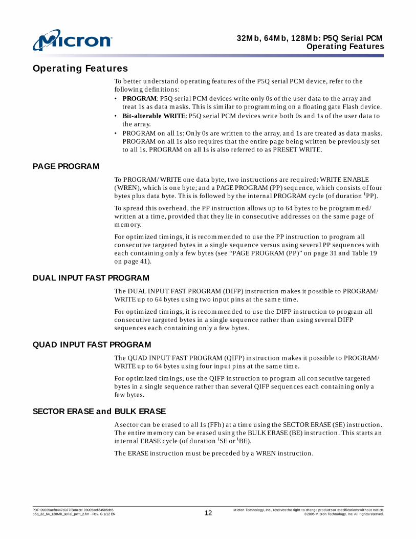
PAGE PROGRAM
To PROGRAM/WRITE one data byte, two instructions are required: WRITE ENABLE (WREN), which is one byte; and a PAGE PROGRAM (PP) sequence, which consists of four bytes plus data byte. This is followed by the internal PROGRAM cycle (of duration tPP).
To spread this overhead, the PP instruction allows up to 64 bytes to be programmed/written at a time, provided that they lie in consecutive addresses on the same page of memory.
For optimized timings, it is recommended to use the PP instruction to program all consecutive targeted bytes in a single sequence versus using several PP sequences with each containing only a few bytes (see “PAGE PROGRAM (PP)” on page 31 and Table 19 on page 41).
DUAL INPUT FAST PROGRAM
The DUAL INPUT FAST PROGRAM (DIFP) instruction makes it possible to PROGRAM/WRITE up to 64 bytes using two input pins at the same time.
For optimized timings, it is recommended to use the DIFP instruction to program all consecutive targeted bytes in a single sequence rather than using several DIFP sequences each containing only a few bytes.
QUAD INPUT FAST PROGRAM
The QUAD INPUT FAST PROGRAM (QIFP) instruction makes it possible to PROGRAM/WRITE up to 64 bytes using four input pins at the same time.
For optimized timings, use the QIFP instruction to program all consecutive targeted bytes in a single sequence rather than several QIFP sequences each containing only a few bytes.
SECTOR ERASE and BULK ERASE
A sector can be erased to all 1s (FFh) at a time using the SECTOR ERASE (SE) instruction. The entire memory can be erased using the BULK ERASE (BE) instruction. This starts an internal ERASE cycle (of duration tSE or tBE).
The ERASE instruction must be preceded by a WREN instruction.
PDF: 09005aef8447d377/Source: 09005aef845b5cb5 Micron Technology, Inc., reserves the right to change products or specifications without notice.p5q_32_64_128Mb_serial_pcm_2.fm - Rev. G 1/12 EN 12 ©2005 Micron Technology, Inc. All rights reserved.

32Mb, 64Mb, 128Mb: P5Q Serial PCMOperating Features
Polling During a WRITE, PROGRAM, or ERASE Cycle
Additional improvements in the time to WRSR, PP, DIFP, QIFP, or ERASE (SE or BE) can be achieved by not waiting for the worst case delay (tW, tPP, tSMEN, tSMEX, tSE, or tBE). The write in progress (WIP) bit is provided in the status register so that the application program can monitor its value, polling it to establish when the previous WRITE cycle, PROGRAM cycle, or ERASE cycle is complete.
Active Power and Standby Power
When S# is LOW, the device is selected and is in the active power mode. When S# is HIGH, the device is deselected, but could remain in the active power mode until all internal cycles have completed (PROGRAM, ERASE, WRITE STATUS REGISTER). The device then goes in to the standby power mode. The device consumption drops to ICC1.
Status Register
The status register contains a number of status and control bits that can be read or set (as appropriate) by specific instructions. See “READ STATUS REGISTER (RDSR)” on page 24 for a detailed description of the status register bits.
Protocol-Related Protections
The environments where nonvolatile memory devices are used can be very noisy, but SPI devices cannot operate correctly in the presence of excessive noise. To help combat this, the P5Q serial PCM features the following data protection mechanisms:• Power on reset and an internal timer (tPUW) can provide protection against inadver-
tent changes while the power supply is outside the operating specification.• PROGRAM, ERASE, and WRITE STATUS REGISTER are checked to ensure they consist
of a number of clock pulses that is a multiple of eight before they are accepted for execution.
• All instructions that modify data must be preceded by a WREN instruction to set the WEL bit. This bit is returned to its reset state by the following events:– Power-up– WRDI instruction completion– WRSR instruction completion– PP instruction completion– DIFP instruction completion– QIFP instruction completion– SE instruction completion– BE instruction completion
• The block protect bits and top/bottom bit enable part of the memory to be configured as read-only. This is the software protect mode (SPM).
• The W# signal enables the block protect bits (BP3, BP2, BP1, BP0), top/bottom (TB) bit, and status register write disable (SRWD) bit to be protected. This is the hardware protected mode (HPM).
PDF: 09005aef8447d377/Source: 09005aef845b5cb5 Micron Technology, Inc., reserves the right to change products or specifications without notice.p5q_32_64_128Mb_serial_pcm_2.fm - Rev. G 1/12 EN 13 ©2005 Micron Technology, Inc. All rights reserved.

32Mb, 64Mb, 128Mb: P5Q Serial PCMOperating Features
Notes: 1. The device is ready to accept a BULK ERASE instruction if all block protect bits (BP3, BP2, BP1, BP0) are 0.
2. X can be 0 or 1.
Table 2: 32Mb Protected Area Size
Status Register Contents Memory Content
TB Bit BP Bit 3 BP Bit 2 BP Bit 1 BP Bit 0 Protected Area Unprotected Area
0 0 0 0 0 None All sectors1 (sectors 0 to 31)0 0 0 0 1 Upper 32nd (sector 31) Sectors 0 to 300 0 0 1 0 Upper 16th (sectors 30 to 31) Sectors 0 to 290 0 0 1 1 Upper 8th (sectors 28 to 31) Sectors 0 to 270 0 1 0 0 Upper 4th (sectors 24 to 31) Sectors 0 to 230 0 1 0 1 Upper half (sectors 16 to 31) Sectors 0 to 150 0 1 1 0 All sectors (sectors 0 to 31) None0 0 1 1 1 All sectors (sectors 0 to 31) None0 1 X2 X2 X2 All sectors (sectors 0 to 31) None1 0 0 0 0 None All sectors1 (sectors 0 to 31)1 0 0 0 1 Lower 32nd (sector 0) Sectors 1 to 311 0 0 1 0 Lower 16th (sectors 0 to 1) Sectors 2 to 311 0 0 1 1 Lower 8th (sectors 0 to 3) Sectors 4 to 311 0 1 0 0 Lower 4th (sectors 0 to 7) Sectors 8 to 311 0 1 0 1 Lower half (sectors 0 to 15) Sectors 16 to 311 0 1 1 0 All sectors (sectors 0 to 31) None1 0 1 1 1 All sectors (sectors 0 to 31) None1 1 X2 X2 X2 All sectors (sectors 0 to 31) None
PDF: 09005aef8447d377/Source: 09005aef845b5cb5 Micron Technology, Inc., reserves the right to change products or specifications without notice.p5q_32_64_128Mb_serial_pcm_2.fm - Rev. G 1/12 EN 14 ©2005 Micron Technology, Inc. All rights reserved.

32Mb, 64Mb, 128Mb: P5Q Serial PCMOperating Features
Notes: 1. The device is ready to accept a BULK ERASE instruction if all block protect bits (BP3, BP2, BP1, BP0) are 0.
2. X can be 0 or 1.
Table 3: 64Mb Protected Area Size
Status Register Contents Memory Content
TB Bit BP Bit 3 BP Bit 2 BP Bit 1 BP Bit 0 Protected Area Unprotected Area
0 0 0 0 0 None All sectors1 (sectors 0 to 63)0 0 0 0 1 Upper 64th (sector 63) Sectors 0 to 620 0 0 1 0 Upper 32nd (sectors 62 to 63) Sectors 0 to 610 0 0 1 1 Upper 16th (sectors 60 to 63) Sectors 0 to 590 0 1 0 0 Upper 8th (sectors 56 to 63) Sectors 0 to 550 0 1 0 1 Upper 4th (sectors 48 to 63) Sectors 0 to 470 0 1 1 0 Upper half (sectors 32 to 63) Sectors 0 to 310 0 1 1 1 All sectors (sectors 0 to 31) None0 1 X2 X2 X2 All sectors (sectors 0 to 31) None1 0 0 0 0 None All sectors1 (sectors 0 to 63)1 0 0 0 1 Lower 64th (sector 0) Sectors 1 to 631 0 0 1 0 Lower 32nd (sectors 0 to 1) Sectors 2 to 631 0 0 1 1 Lower 16th (sectors 0 to 3) Sectors 4 to 631 0 1 0 0 Lower 8th (sectors 0 to 7) Sectors 8 to 631 0 1 0 1 Lower 4th (sectors 0 to 15) Sectors 16 to 631 0 1 1 0 Lower half (sectors 0 to 31) Sectors 32 to 631 0 1 1 1 All sectors (sectors 0 to 63) None1 1 X2 X2 X2 All sectors (sectors 0 to 63) None
PDF: 09005aef8447d377/Source: 09005aef845b5cb5 Micron Technology, Inc., reserves the right to change products or specifications without notice.p5q_32_64_128Mb_serial_pcm_2.fm - Rev. G 1/12 EN 15 ©2005 Micron Technology, Inc. All rights reserved.

32Mb, 64Mb, 128Mb: P5Q Serial PCMOperating Features
Notes: 1. The device is ready to accept a BULK ERASE instruction if all block protect bits (BP3, BP2, BP1, BP0) are 0.
2. X can be 0 or 1.
Hold Condition
The Hold (HOLD#) signal is used to pause any serial communications with the device without resetting the clocking sequence. However, taking this signal LOW does not terminate any WRITE STATUS REGISTER, PROGRAM, or ERASE cycle that is currently in progress.
To enter the hold condition, the device must be selected, with S# LOW. The hold condi-tion starts on the falling edge of the HOLD# signal, provided that this coincides with C being LOW (as shown in Figure 5 on page 17). The hold condition ends on the rising edge of the HOLD# signal, provided that this coincides with C being LOW.
If the falling edge does not coincide with C being LOW, the hold condition starts after the next time C goes LOW. Similarly, if the rising edge does not coincide with C being LOW, the hold condition ends after C next goes LOW (as shown in Figure 5 on page 17).
During the hold condition, DQ1 is High-Z, and DQ0 and C are “Don’t Care.”
Normally, the device is kept selected, with S# driven LOW, for the whole duration of the hold condition. This is to ensure that the state of the internal logic remains unchanged from the moment of entering the hold condition.
If S# goes HIGH while the device is in the hold condition, this has the effect of resetting the internal logic of the device. To restart communication with the device, it is necessary to drive HOLD# HIGH, and then to drive S# LOW. This prevents the device from going back to the hold condition.
Table 4: 128Mb Protected Area Size
Status Register Contents Memory Content
TB Bit BP Bit 3 BP Bit 2 BP Bit 1 BP Bit 0 Protected Area Unprotected Area
0 0 0 0 0 None All sectors1 (sectors 0 to 127)0 0 0 0 1 Upper 128 (sector 127) Sectors 0 to 1260 0 0 1 0 Upper 64 (sectors 126 to 127) Sectors 0 to 1250 0 0 1 1 Upper 32 (sectors 124 to 127) Sectors 0 to 1230 0 1 0 0 Upper 16 (sectors 120 to 127) Sectors 0 to 1190 0 1 0 1 Upper 8 (sectors 112 to 127) Sectors 0 to 1110 0 1 1 0 Upper quarter
(sectors 96 to 127)Sectors 0 to 95
0 0 1 1 1 Upper half (sectors 64 to 127) Sectors 0 to 630 1 X2 X2 X2 All sectors (sectors 0 to 127) None1 0 0 0 0 None All sectors1 (sectors 0 to 127)1 0 0 0 1 Lower 128 (sector 0) Sectors 1 to 1271 0 0 1 0 Lower 64 (sectors 0 to 1) Sectors 2 to 1271 0 0 1 1 Lower 32 (sectors 0 to 3) Sectors 4 to 1271 0 1 0 0 Lower 16 (sectors 0 to 7) Sectors 8 to 1271 0 1 0 1 Lower 8 (sectors 0 to 15) Sectors 16 to 1271 0 1 1 0 Lower 4 (sectors 0 to 31) Sectors 32 to 1271 0 1 1 1 Lower half (sectors 0 to 63) Sectors 64 to 1271 1 X2 X2 X2 All sectors (sectors 0 to 127) None
PDF: 09005aef8447d377/Source: 09005aef845b5cb5 Micron Technology, Inc., reserves the right to change products or specifications without notice.p5q_32_64_128Mb_serial_pcm_2.fm - Rev. G 1/12 EN 16 ©2005 Micron Technology, Inc. All rights reserved.

32Mb, 64Mb, 128Mb: P5Q Serial PCMMemory Organization
Figure 5: Hold Condition Activation
Memory OrganizationFor the 32Mb part, the memory is organized as:• 4,193,054 bytes (8 bits each)• 32 sectors (128KB each)• 65,536 pages (64 bytes each)
For the 64Mb part, the memory is organized as:• 8,386,108 bytes (8 bits each)• 64 sectors (128KB each)• 131,072 pages (64 bytes each)
For the 128Mb part, the memory is organized as:• 16,772,216 bytes (8 bits each)• 8 super page programming regions (16 sectors each)• 128 sectors (128KB each)• 262,144 pages (64 bytes each)
Each page can be individually programmed (bits are programmed from 1 to 0) or written (bit alterable: 1 can be altered to 0 and 0 can be altered to 1). The device is sector or bulk erasable (bits are erased from 0 to 1).
HOLD#
C
Holdcondition
(standard use)
Holdcondition
(non-standard use)
PDF: 09005aef8447d377/Source: 09005aef845b5cb5 Micron Technology, Inc., reserves the right to change products or specifications without notice.p5q_32_64_128Mb_serial_pcm_2.fm - Rev. G 1/12 EN 17 ©2005 Micron Technology, Inc. All rights reserved.

32Mb, 64Mb, 128Mb: P5Q Serial PCMMemory Organization
Table 5: 32Mb Memory Map
Sector Address Range Sector Address Range
15 1E0000 1FFFFF 31 3E0000 3FFFFF14 1C0000 1DFFFF 30 3C0000 3DFFFF13 1A0000 1BFFFF 29 3A0000 3BFFFF12 180000 19FFFF 28 380000 39FFFF11 160000 17FFFF 27 360000 37FFFF10 140000 15FFFF 26 340000 35FFFF9 120000 13FFFF 25 320000 33FFFF8 100000 11FFFF 24 300000 31FFFF7 0E0000 0FFFFF 23 2E0000 2FFFFF6 0C0000 0DFFFF 22 2C0000 2DFFFF5 0A0000 0BFFFF 21 2A0000 2BFFFF4 080000 09FFFF 20 280000 29FFFF3 060000 07FFFF 19 260000 27FFFF2 040000 05FFFF 18 240000 25FFFF1 020000 03FFFF 17 220000 23FFFF0 000000 01FFFF 16 200000 21FFFF
PDF: 09005aef8447d377/Source: 09005aef845b5cb5 Micron Technology, Inc., reserves the right to change products or specifications without notice.p5q_32_64_128Mb_serial_pcm_2.fm - Rev. G 1/12 EN 18 ©2005 Micron Technology, Inc. All rights reserved.

32Mb, 64Mb, 128Mb: P5Q Serial PCMMemory Organization
Table 6: 64Mb Memory Map
Sector Address Range Sector Address Range
31 3E0000 3FFFFF 63 7E0000 7FFFFF30 3C0000 3DFFFF 62 7C0000 7DFFFF29 3A0000 3BFFFF 61 7A0000 7BFFFF28 380000 39FFFF 60 780000 79FFFF27 360000 37FFFF 59 760000 77FFFF26 340000 35FFFF 58 740000 75FFFF25 320000 33FFFF 57 720000 73FFFF24 300000 31FFFF 56 700000 71FFFF23 2E0000 2FFFFF 55 6E0000 6FFFFF22 2C0000 2DFFFF 54 6C0000 6DFFFF21 2A0000 2BFFFF 53 6A0000 6BFFFF20 280000 29FFFF 52 680000 69FFFF19 260000 27FFFF 51 660000 67FFFF18 240000 25FFFF 50 640000 65FFFF17 220000 23FFFF 49 620000 63FFFF16 200000 21FFFF 48 600000 61FFFF15 1E0000 1FFFFF 47 5E0000 5FFFFF14 1C0000 1DFFFF 46 5C0000 5DFFFF13 1A0000 1BFFFF 45 5A0000 5BFFFF12 180000 19FFFF 44 580000 59FFFF11 160000 17FFFF 43 560000 57FFFF10 140000 15FFFF 42 5400 00 55FFFF9 120000 13FFFF 41 520000 53FFFF8 100000 11FFFF 40 500000 51FFFF7 0E0000 0FFFFF 39 4E0000 4FFFFF6 0C0000 0DFFFF 38 4C0000 4DFFFF5 0A0000 0BFFFF 37 4A0000 4BFFFF4 080000 09FFFF 36 480000 49FFFF3 060000 07FFFF 35 460000 47FFFF2 040000 05FFFF 34 440000 45FFFF1 020000 03FFFF 33 420000 43FFFF0 000000 01FFFF 32 400000 41FFFF
PDF: 09005aef8447d377/Source: 09005aef845b5cb5 Micron Technology, Inc., reserves the right to change products or specifications without notice.p5q_32_64_128Mb_serial_pcm_2.fm - Rev. G 1/12 EN 19 ©2005 Micron Technology, Inc. All rights reserved.

32Mb, 64Mb, 128Mb: P5Q Serial PCMMemory Organization
Table 7: 128Mb Memory Map
Sector Address Range Sector Address Range
63 7E0000 7FFFFF 127 FE0000 FFFFFF62 7C0000 7DFFFF 126 FC0000 FDFFFF61 7A0000 7BFFFF 125 FA0000 FBFFFF60 780000 79FFFF 124 F80000 F9FFFF59 760000 77FFFF 123 F60000 F7FFFF58 740000 75FFFF 122 F40000 F5FFFF57 720000 73FFFF 121 F20000 F3FFFF56 700000 71FFFF 120 F00000 F1FFFF55 6E0000 6FFFFF 119 EE0000 EFFFFF54 6C0000 6DFFFF 118 EC0000 EDFFFF53 6A0000 6BFFFF 117 EA0000 EBFFFF52 680000 69FFFF 116 E80000 E9FFFF51 660000 67FFFF 115 E60000 E7FFFF50 640000 65FFFF 114 E40000 E5FFFF49 620000 63FFFF 113 E20000 E3FFFF48 600000 61FFFF 112 E00000 E1FFFF47 5E0000 5FFFFF 111 DE0000 DFFFFF46 5C0000 5DFFFF 110 DC0000 DDFFFF45 5A0000 5BFFFF 109 DA0000 DBFFFF44 580000 59FFFF 108 D80000 D9FFFF43 560000 57FFFF 107 D60000 D7FFFF42 540000 55FFFF 106 D40000 D5FFFF41 520000 53FFFF 105 D20000 D3FFFF40 500000 51FFFF 104 D00000 D1FFFF39 4E0000 4FFFFF 103 CE0000 CFFFFF38 4C0000 4DFFFF 102 CC0000 CDFFFF37 4A0000 4BFFFF 101 CA0000 CBFFFF36 480000 49FFFF 100 C80000 C9FFFF35 460000 47FFFF 99 C60000 C7FFFF34 440000 45FFFF 98 C40000 C5FFFF33 420000 43FFFF 97 C20000 C3FFFF32 400000 41FFFF 96 C00000 C1FFFF31 3E0000 3FFFFF 95 BE0000 BFFFFF30 3C0000 3DFFFF 94 BC0000 BDFFFF29 3A0000 3BFFFF 93 BA0000 BBFFFF28 380000 39FFFF 92 B80000 B9FFFF27 360000 37FFFF 91 B60000 B7FFFF26 340000 35FFFF 90 B40000 B5FFFF25 320000 33FFFF 89 B20000 B3FFFF24 300000 31FFFF 88 B00000 B1FFFF23 2E0000 2FFFFF 87 AE0000 AFFFFF22 2C0000 2DFFFF 86 AC0000 ADFFFF21 2A0000 2BFFFF 85 AA0000 ABFFFF20 280000 29FFFF 84 A80000 A9FFFF19 260000 27FFFF 83 A60000 A7FFFF18 240000 25FFFF 82 A40000 A5FFFF
PDF: 09005aef8447d377/Source: 09005aef845b5cb5 Micron Technology, Inc., reserves the right to change products or specifications without notice.p5q_32_64_128Mb_serial_pcm_2.fm - Rev. G 1/12 EN 20 ©2005 Micron Technology, Inc. All rights reserved.

32Mb, 64Mb, 128Mb: P5Q Serial PCMInstructions
InstructionsAll instructions, addresses, and data are shifted in and out of the device, most significant bit first.
Serial data input DQ0 is sampled on the first rising edge of C after S# is driven LOW. Then, the one-byte instruction code must be shifted in to the device, most significant bit first, on serial data input DQ0, each bit being latched on the rising edges of C. The instruction set is listed in Table 8 on page 22.
Every instruction sequence starts with a one-byte instruction code. Depending on the instruction, this might be followed by address bytes, data bytes, both, or none.
In the case of read data bytes (READ), read data bytes at higher speed (FAST_READ), DOFR, QOFR, RDSR, or READ IDENTIFICATION (RDID) instruction, the shifted-in instruction sequence is followed by a data-out sequence. S# can be driven HIGH after any bit of the data-out sequence is being shifted out.
In the case of a PP, DIFP, QIFP, SE, BE, WRSR, WREN, or WRDI, S# must be driven HIGH exactly at a byte boundary; otherwise the instruction is rejected and is not executed. That is, S# must be driven HIGH when the number of clock pulses after S# being driven LOW is an exact multiple of eight.
All attempts to access the memory array during a WRITE STATUS REGISTER cycle, PROGRAM cycle, or ERASE cycle are ignored and the internal WRITE STATUS REGISTER cycle, PROGRAM cycle, ERASE cycle continues unaffected.
Note: Output High-Z is defined as the point where data out is no longer driven.
17 220000 23FFFF 81 A20000 A3FFFF16 200000 21FFFF 80 A00000 A1FFFF15 1E0000 1FFFFF 79 9E0000 9FFFFF14 1C0000 1DFFFF 78 9C0000 9DFFFF13 1A0000 1BFFFF 77 9A0000 9BFFFF12 180000 19FFFF 76 980000 99FFFF11 160000 17FFFF 75 960000 97FFFF10 140000 15FFFF 74 940000 95FFFF9 120000 13FFFF 73 920000 93FFFF8 100000 11FFFF 72 900000 91FFFF7 0E0000 0FFFFF 71 8E0000 8FFFFF6 0C0000 0DFFFF 70 8C0000 8DFFFF5 0A0000 0BFFFF 69 8A0000 8BFFFF4 080000 09FFFF 68 880000 89FFFF3 060000 07FFFF 67 860000 87FFFF2 040000 05FFFF 66 840000 85FFFF1 020000 03FFFF 65 820000 83FFFF0 000000 01FFFF 64 800000 81FFFF
Table 7: 128Mb Memory Map (Continued)
Sector Address Range Sector Address Range
PDF: 09005aef8447d377/Source: 09005aef845b5cb5 Micron Technology, Inc., reserves the right to change products or specifications without notice.p5q_32_64_128Mb_serial_pcm_2.fm - Rev. G 1/12 EN 21 ©2005 Micron Technology, Inc. All rights reserved.

32Mb, 64Mb, 128Mb: P5Q Serial PCMInstructions
WRITE ENABLE (WREN)
The WRITE ENABLE (WREN) instruction sets the WEL bit. The WEL bit must be set prior to every PP, DIFP, SE, BE, or WRSR instruction.
The WREN instruction is entered by driving S# LOW, sending the instruction code, and then driving S# HIGH.
Figure 6: WRITE ENABLE (WREN) Instruction Sequence
Table 8: Instruction Set
Instruction Description One-Byte Instruction CodeAddress
BytesDummy
BytesData Bytes
WREN Write enable 0000 0110 06h 0 0 0 WRDI Write disable 0000 0100 04h 0 0 0 RDID Read identification 1001 1111 9Fh 0 0 1 to 3
1001 1110 9Eh 0 0 1 to 3RDSR Read status register 0000 0101 05h 0 0 1 to ∞WRSR Write status register 0000 0001 01h 0 0 1 READ Read data bytes 0000 0011 03h 3 0 1 to ∞
FAST_READ Read data bytes at higher speed 0000 1011 0Bh 3 1 1 to ∞DOFR Dual output fast read 0011 1011 3Bh 3 1 1 to ∞QOFR Quad output fast read 0110 1011 6Bh 3 1 1 to ∞
PP Page program (legacy program) 0000 0010 02h 3 0 1 to 64
Page program (bit-alterable write) 0010 0010 22h 3 0 1 to 64
Page program (on all 1s) 1101 0001 D1h 3 0 1 to 64DIFP Dual input fast program (legacy
program)1010 0010 A2h 3 0 1 to 64
Dual input fast program (bit-alterable write)
1101 0011 D3h 3 0 1 to 64
Dual input fast program (on all 1s) 1101 0101 D5h 3 0 1 to 64QIFP Quad input fast program (legacy
program)0011 0010 32h 3 0 1 to 64
Quad input fast program (bit-alterable write)
1101 0111 D7h 3 0 1 to 64
Quad input fast program (on all 1s) 1101 1001 D9h 3 0 1 to 64SE Sector erase 1101 1000 D8h 3 0 0 BE Bulk erase 1100 0111 C7h 0 0 0
C
DQ0
S#
21 3 4 5 6 7
Command
0
DQ1High-Z
PDF: 09005aef8447d377/Source: 09005aef845b5cb5 Micron Technology, Inc., reserves the right to change products or specifications without notice.p5q_32_64_128Mb_serial_pcm_2.fm - Rev. G 1/12 EN 22 ©2005 Micron Technology, Inc. All rights reserved.
32Mb, 64Mb, 128Mb: P5Q Serial PCMInstructions
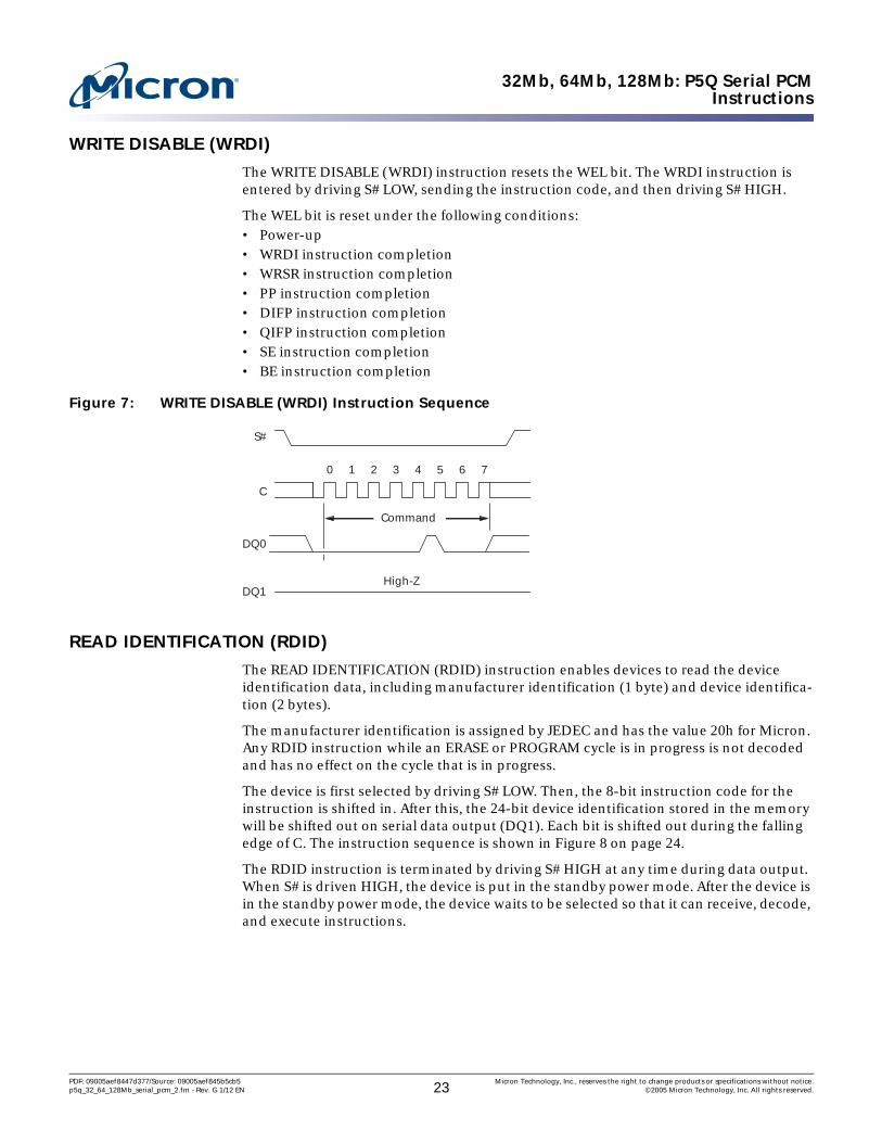
WRITE DISABLE (WRDI)
The WRITE DISABLE (WRDI) instruction resets the WEL bit. The WRDI instruction is entered by driving S# LOW, sending the instruction code, and then driving S# HIGH.
The WEL bit is reset under the following conditions: • Power-up• WRDI instruction completion• WRSR instruction completion• PP instruction completion• DIFP instruction completion• QIFP instruction completion• SE instruction completion• BE instruction completion
Figure 7: WRITE DISABLE (WRDI) Instruction Sequence
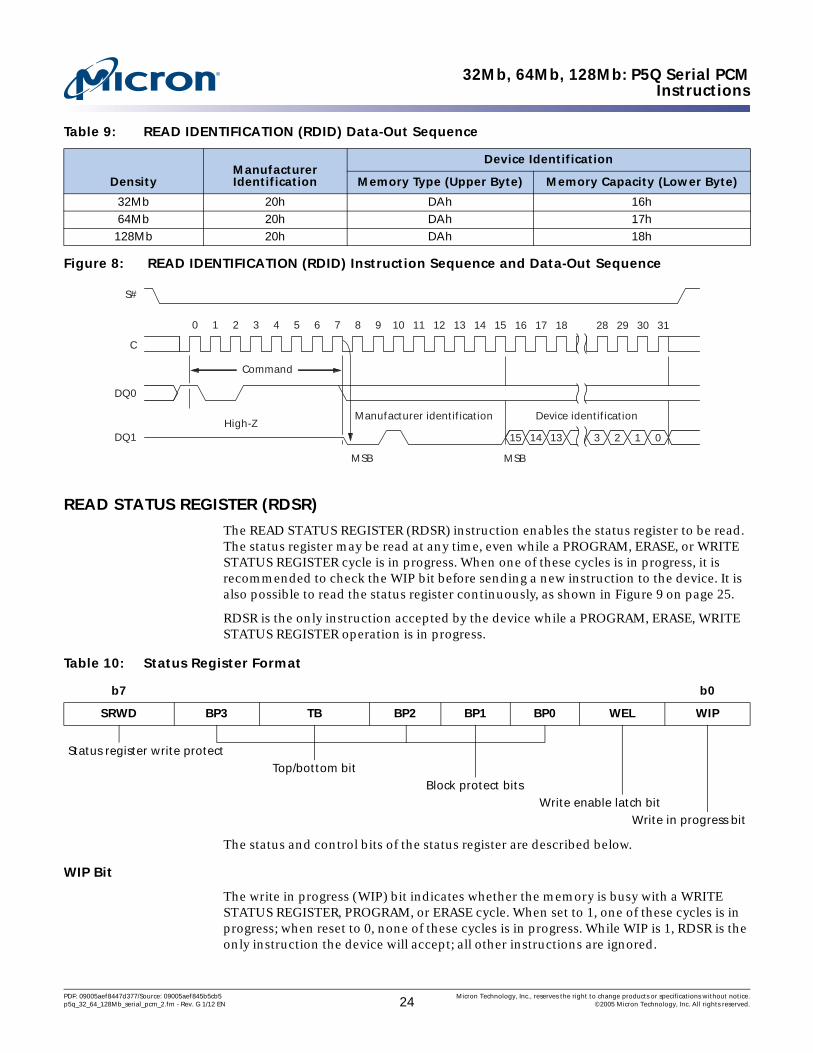
READ IDENTIFICATION (RDID)
The READ IDENTIFICATION (RDID) instruction enables devices to read the device identification data, including manufacturer identification (1 byte) and device identifica-tion (2 bytes).
The manufacturer identification is assigned by JEDEC and has the value 20h for Micron. Any RDID instruction while an ERASE or PROGRAM cycle is in progress is not decoded and has no effect on the cycle that is in progress.
The device is first selected by driving S# LOW. Then, the 8-bit instruction code for the instruction is shifted in. After this, the 24-bit device identification stored in the memory will be shifted out on serial data output (DQ1). Each bit is shifted out during the falling edge of C. The instruction sequence is shown in Figure 8 on page 24.
The RDID instruction is terminated by driving S# HIGH at any time during data output. When S# is driven HIGH, the device is put in the standby power mode. After the device is in the standby power mode, the device waits to be selected so that it can receive, decode, and execute instructions.
C
DQ0
S#
21 3 4 5 6 7
Command
0
DQ1High-Z
PDF: 09005aef8447d377/Source: 09005aef845b5cb5 Micron Technology, Inc., reserves the right to change products or specifications without notice.p5q_32_64_128Mb_serial_pcm_2.fm - Rev. G 1/12 EN 23 ©2005 Micron Technology, Inc. All rights reserved.
32Mb, 64Mb, 128Mb: P5Q Serial PCMInstructions
Figure 8: READ IDENTIFICATION (RDID) Instruction Sequence and Data-Out Sequence
READ STATUS REGISTER (RDSR)
The READ STATUS REGISTER (RDSR) instruction enables the status register to be read. The status register may be read at any time, even while a PROGRAM, ERASE, or WRITE STATUS REGISTER cycle is in progress. When one of these cycles is in progress, it is recommended to check the WIP bit before sending a new instruction to the device. It is also possible to read the status register continuously, as shown in Figure 9 on page 25.
RDSR is the only instruction accepted by the device while a PROGRAM, ERASE, WRITE STATUS REGISTER operation is in progress.
The status and control bits of the status register are described below.
WIP Bit
The write in progress (WIP) bit indicates whether the memory is busy with a WRITE STATUS REGISTER, PROGRAM, or ERASE cycle. When set to 1, one of these cycles is in progress; when reset to 0, none of these cycles is in progress. While WIP is 1, RDSR is the only instruction the device will accept; all other instructions are ignored.
Table 9: READ IDENTIFICATION (RDID) Data-Out Sequence
DensityManufacturer Identification
Device Identification
Memory Type (Upper Byte) Memory Capacity (Lower Byte)
32Mb 20h DAh 16h64Mb 20h DAh 17h
128Mb 20h DAh 18h
Table 10: Status Register Format
b7 b0
SRWD BP3 TB BP2 BP1 BP0 WEL WIP
Status register write protectTop/bottom bit
Block protect bitsWrite enable latch bit
Write in progress bit
15 14 13 3 2 1 0
C
DQ0
S#
21 3 4 5 6 7 8 9 10 11 12 13 14 15
Command
0
DQ1
Manufacturer identificationHigh-Z
MSB
Device identification
MSB
16 17 18 28 29 30 31
PDF: 09005aef8447d377/Source: 09005aef845b5cb5 Micron Technology, Inc., reserves the right to change products or specifications without notice.p5q_32_64_128Mb_serial_pcm_2.fm - Rev. G 1/12 EN 24 ©2005 Micron Technology, Inc. All rights reserved.

32Mb, 64Mb, 128Mb: P5Q Serial PCMInstructions
WEL Bit
The write enable latch (WEL) bit indicates the status of the internal write enable latch. When set to 1, the internal write enable latch is set. When it is set to 0, the internal write enable latch is reset, and no WRITE STATUS REGISTER, PROGRAM, or ERASE instruc-tion is accepted.
Block Protect Bits
The block protect bits (BP3, BP2, BP1, BP0) are nonvolatile. They define the size of the area to be software protected against PROGRAM (or WRITE) and ERASE instructions. These bits are written with the WRSR instruction. When one or more of the block protect bits is set to 1, the relevant memory area (as defined in Table 2 on page 14) becomes protected against PP, DIFP, QIFP, and SE instructions. The block protect bits can be written, provided that the hardware protected mode has not been set. The BE instruc-tion is executed if all block protect bits are 0.
Top/Bottom Bit
The top/bottom (TB) bit is nonvolatile. It can be set and reset with the WRSR instruc-tion, provided that the WREN instruction has been issued. The TB bit is used in conjunc-tion with the block protect bits to determine if the protected area defined by the block protect bits starts from the top or the bottom of the memory array.• When TB bit is reset to 0 (default value), the area protected by the block protect bits
starts from the top of the memory array (see Table 2 on page 14)• When TB bit is set to 1, the area protected by the block protect bits starts from the
bottom of the memory array (see Table 2 on page 14).
The TB bit cannot be written when the SRWD bit is set to 1 and the W# pin is driven LOW.
SRWD Bit
The status register write disable (SRWD) bit is operated in conjunction with the W# signal. The SRWD bit and the W# signal allow the device to be put in the hardware protected mode (when the SRWD bit is set to 1 and W# is driven LOW). In this mode, the nonvolatile bits of the status register (SRWD, TB, BP3, BP2, BP1, BP0) become read-only bits and the WRSR instruction is no longer accepted for execution.
Figure 9: READ STATUS REGISTER (RDSR) Instruction Sequence and Data-Out Sequence
7 76 5 4 3 2 1 07 6 5 4 3 2 1 0
C
DQ0
S#
21 3 4 5 6 7 8 9 10 11 12 13 14 15
Command
0
DQ1
Status register outHigh-Z
MSB
Status register out
MSB
PDF: 09005aef8447d377/Source: 09005aef845b5cb5 Micron Technology, Inc., reserves the right to change products or specifications without notice.p5q_32_64_128Mb_serial_pcm_2.fm - Rev. G 1/12 EN 25 ©2005 Micron Technology, Inc. All rights reserved.

32Mb, 64Mb, 128Mb: P5Q Serial PCMInstructions
WRITE STATUS REGISTER (WRSR)
The WRITE STATUS REGISTER (WRSR) instruction enables new values to be written to the status register. Before it can be accepted, a WREN instruction must previously have been executed. After the WREN instruction has been decoded and executed, the device sets the WEL.
The WRSR instruction is entered by driving S# LOW, followed by the instruction code and the data byte on serial data input (DQ0). The instruction sequence is shown in Figure 10 on page 26. The WRSR instruction has no effect on B1 and B0 of the status register.
S# must be driven HIGH after the eighth bit of the data byte has been latched in. If not, the WRSR instruction is not executed. As soon as S# is driven HIGH, the self-timed WRITE STATUS REGISTER cycle (whose duration is tW) is initiated. While the WRITE STATUS REGISTER cycle is in progress, the status register may still be read to check the value of the WIP bit. The WIP bit is 1 during the self-timed WRITE STATUS REGISTER cycle, and is 0 when it is completed. When the cycle is completed, the WEL is reset.
The WRSR instruction enables the user to change the values of the block protect bits and to define the size of the area that is to be treated as read-only, as defined in Table 2 on page 14. The WRSR instruction also enables the user to set and reset the SRWD bit in accordance with the W# signal. The SRWD bit and W# signal enable the device to be put in the hardware protected mode (HPM). The WRSR instruction is not executed after the HPM is entered.
RDSR is the only instruction that is accepted while a WRSR operation is in progress; all other instructions are ignored.
Figure 10: WRITE STATUS REGISTER (WRSR) Instruction Sequence
7 6 5 4 3 2 1 0
C
DQ0
S#
21 3 4 5 6 7 8 9 10 11 12 13 14 15
Command
0
DQ1
Statusregister in
High-ZMSB
PDF: 09005aef8447d377/Source: 09005aef845b5cb5 Micron Technology, Inc., reserves the right to change products or specifications without notice.p5q_32_64_128Mb_serial_pcm_2.fm - Rev. G 1/12 EN 26 ©2005 Micron Technology, Inc. All rights reserved.

32Mb, 64Mb, 128Mb: P5Q Serial PCMInstructions
Notes: 1. As defined by the values in the block protect bits (BP3, BP2, BP1, BP0) of the status register, as shown in Table 2 on page 14.
When the SRWD bit of the status register is 0 (its initial delivery state), it is possible to write to the status register, provided that the WEL bit has previously been set by a WREN instruction, regardless of whether W# is driven HIGH or LOW.
When the SRWD bit of the status register is set to 1, two cases need to be considered, depending on the state of W#:• If W# is driven HIGH, it is possible to write to the status register provided that the WEL
bit has previously been set by a WREN instruction.• If W# is driven LOW, it is not possible to write to the status register even if the WEL bit
has previously been set by a WREN instruction (attempts to write to the status register are rejected and are not accepted for execution). As a consequence, all the data bytes in the memory area that are software protected (SPM) by the block protect bits of the status register are also hardware protected against data modification.
Regardless of the order of the two events, the HPM can be entered in one of two ways:• Set the SRWD bit after driving W# LOW.• Drive W# LOW after setting the SRWD bit.
The only way to exit HPM after it has been entered is to pull write protect (W#) HIGH.
If write protect (W#) is permanently tied HIGH, HPM can never be activated, and only the software protected mode (SPM), using the block protect bits of the status register, can be used.
Read Data Bytes (READ)
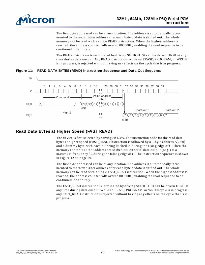
The device is first selected by driving S# LOW. The instruction code for the read data bytes (READ) instruction is followed by a 3-byte address A[23:0], with each bit being latched in during the rising edge of C. Then the memory contents at that address are shifted out on serial data output (DQ1), with each bit being shifted out at a maximum frequency fR, during the falling edge of C. The instruction sequence is shown in Figure 11 on page 28.
Table 11: Protection Modes
W#SRWD
Bit ModeWrite Protection of
Status Register
Memory Content
Protected Area1 Unprotected Area1
1 0 Software protected (SPM)
Status register is writable (if the WREN instruction has set the WEL bit); the values in
the SRWD, TB, BP3, BP2, BP1, and BP0 bits can be
changed
Protected against PAGE PROGRAM, SECTOR
ERASE, and BULK ERASE
Ready to accept PAGE PROGRAM, and SECTOR
ERASE instructions0 01 1
0 1 Hardware protected (HPM)
Status register is hardware write
protected; the values in the SRWD, TB, BP3, BP2, BP1, and BP0 bits cannot
be changed
Protected against PAGE PROGRAM, SECTOR
ERASE, and BULK ERASE
Ready to accept PAGE PROGRAM, and SECTOR
ERASE instructions
PDF: 09005aef8447d377/Source: 09005aef845b5cb5 Micron Technology, Inc., reserves the right to change products or specifications without notice.p5q_32_64_128Mb_serial_pcm_2.fm - Rev. G 1/12 EN 27 ©2005 Micron Technology, Inc. All rights reserved.
32Mb, 64Mb, 128Mb: P5Q Serial PCMInstructions
The first byte addressed can be at any location. The address is automatically incre-mented to the next higher address after each byte of data is shifted out. The whole memory can be read with a single READ instruction. When the highest address is reached, the address counter rolls over to 000000h, enabling the read sequence to be continued indefinitely.
The READ instruction is terminated by driving S# HIGH. S# can be driven HIGH at any time during data output. Any READ instruction, while an ERASE, PROGRAM, or WRITE is in progress, is rejected without having any effects on the cycle that is in progress.
Figure 11: READ DATA BYTES (READ) Instruction Sequence and Data-Out Sequence
Read Data Bytes at Higher Speed (FAST_READ)
The device is first selected by driving S# LOW. The instruction code for the read data bytes at higher speed (FAST_READ) instruction is followed by a 3-byte address A[23:0] and a dummy byte, with each bit being latched in during the rising edge of C. Then the memory contents at that address are shifted out on serial data output (DQ1) at a maximum frequency fC, during the falling edge of C. The instruction sequence is shown in Figure 12 on page 29.
The first byte addressed can be at any location. The address is automatically incre-mented to the next higher address after each byte of data is shifted out. The whole memory can be read with a single FAST_READ instruction. When the highest address is reached, the address counter rolls over to 000000h, enabling the read sequence to be continued indefinitely.
The FAST_READ instruction is terminated by driving S# HIGH. S# can be driven HIGH at any time during data output. While an ERASE, PROGRAM, or WRITE cycle is in progress, any FAST_READ instruction is rejected without having any effects on the cycle that is in progress.
7 6 5 4 3 2 1 0
23 22 21 3 2 1 0
7
C
DQ0
S#
21 3 4 5 6 7 8 9 10
Command
0
DQ1
MSB
High-ZData-out 1
MSB
28 29 30 31 32 33 34 35 36 37 38 39
Data-out 2
24-bit addressnote 1
PDF: 09005aef8447d377/Source: 09005aef845b5cb5 Micron Technology, Inc., reserves the right to change products or specifications without notice.p5q_32_64_128Mb_serial_pcm_2.fm - Rev. G 1/12 EN 28 ©2005 Micron Technology, Inc. All rights reserved.

32Mb, 64Mb, 128Mb: P5Q Serial PCMInstructions
Figure 12: FAST_READ Instruction Sequence and Data-Out Sequence
DUAL OUTPUT FAST READ (DOFR)
The DUAL OUTPUT FAST READ (DOFR) instruction is very similar to the FAST_READ instruction, except that the data are shifted out on two pins (DQ0 and DQ1) instead of one. Outputting the data on two pins instead of one doubles the data transfer bandwidth compared to the outputting data using the FAST_READ instruction.
The device is first selected by driving S# LOW. The instruction code for the DOFR instruction is followed by a 3-byte address A[23:0] and a dummy byte, with each bit being latched-in during the rising edge of serial clock (C). Then the memory contents at that address are shifted out on DQ0 and DQ1 at a maximum frequency fC, during the falling edge of C. The instruction sequence is shown in Figure 13 on page 30.
The first byte addressed can be at any location. The address is automatically incre-mented to the next higher address after each byte of data is shifted out on DQ0 and DQ1. The whole memory can be read with a single DOFR instruction. When the highest address is reached, the address counter rolls over to 00 0000h so that the read sequence can be continued indefinitely.
7 6 5 4 3 2 1 0 7 6 5 4 3 2 1 0
7 6 5 4 3 2 1 0
7
C
DQ0
S#
3433 35 36 37 38 39 40 41 42 43
Dummy cycles
32
DQ1
Data-out 1
MSB MSB MSB
44 45 46 47
Data-out 2
23 22 21 3 2 1 0
C
DQ0
S#
21 3 4 5 6 7 8 9 10
Command
0
DQ1High-Z
28 29 30 31
24-bit addressnote 1
1
1
PDF: 09005aef8447d377/Source: 09005aef845b5cb5 Micron Technology, Inc., reserves the right to change products or specifications without notice.p5q_32_64_128Mb_serial_pcm_2.fm - Rev. G 1/12 EN 29 ©2005 Micron Technology, Inc. All rights reserved.
32Mb, 64Mb, 128Mb: P5Q Serial PCMInstructions
Figure 13: DUAL OUTPUT FAST READ Instruction Sequence
QUAD OUTPUT FAST READ (QOFR)
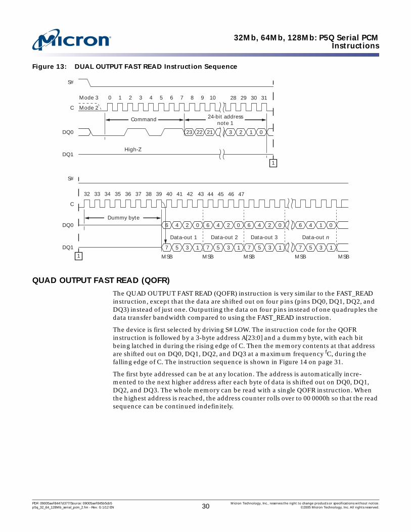
The QUAD OUTPUT FAST READ (QOFR) instruction is very similar to the FAST_READ instruction, except that the data are shifted out on four pins (pins DQ0, DQ1, DQ2, and DQ3) instead of just one. Outputting the data on four pins instead of one quadruples the data transfer bandwidth compared to using the FAST_READ instruction.
The device is first selected by driving S# LOW. The instruction code for the QOFR instruction is followed by a 3-byte address A[23:0] and a dummy byte, with each bit being latched in during the rising edge of C. Then the memory contents at that address are shifted out on DQ0, DQ1, DQ2, and DQ3 at a maximum frequency fC, during the falling edge of C. The instruction sequence is shown in Figure 14 on page 31.
The first byte addressed can be at any location. The address is automatically incre-mented to the next higher address after each byte of data is shifted out on DQ0, DQ1, DQ2, and DQ3. The whole memory can be read with a single QOFR instruction. When the highest address is reached, the address counter rolls over to 00 0000h so that the read sequence can be continued indefinitely.
7 5 3 1 7 5 3 1
C
DQ0
S#
3433 35 36 37 38 39 40 41 42 43
Dummy byte
32
DQ1
Data-out 1
MSB MSBMSB MSBMSB
44 45 46 47
Data-out 2 Data-out 3 Data-out n
6 4 2 0 6 4 2 0 6 4 2 0 6 4 1 0
23 22 21 3 2 1 0
C
DQ0
S#
21 3 4 5 6 7 8 9 10
Command
0Mode 3
Mode 2
DQ1High-Z
28 29 30 31
24-bit addressnote 1
1
1
7 5 3 1 7 5 3 1
PDF: 09005aef8447d377/Source: 09005aef845b5cb5 Micron Technology, Inc., reserves the right to change products or specifications without notice.p5q_32_64_128Mb_serial_pcm_2.fm - Rev. G 1/12 EN 30 ©2005 Micron Technology, Inc. All rights reserved.
32Mb, 64Mb, 128Mb: P5Q Serial PCMInstructions
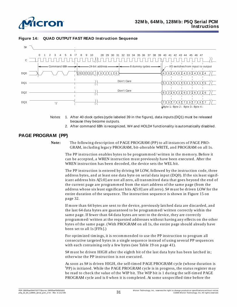
Figure 14: QUAD OUTPUT FAST READ Instruction Sequence
Notes: 1. After 40 clock cycles (cycle labeled 39 in the figure), data inputs (DQ1) must be released because they become outputs.
2. After command 6Bh is recognized, W# and HOLD# functionality is automatically disabled.
PAGE PROGRAM (PP)Note: The following description of PAGE PROGRAM (PP) to all instances of PAGE PRO-
GRAM, including legacy PROGRAM, bit-alterable WRITE, and PROGRAM on all 1s.
The PP instruction enables bytes to be programmed/written in the memory. Before it can be accepted, a WREN instruction must previously have been executed. After the WREN instruction has been decoded, the device sets the WEL bit.
The PP instruction is entered by driving S# LOW, followed by the instruction code, three address bytes, and at least one data byte on serial data input (DQ0). If the six least signif-icant address bits A[5:0] are not all zero, all transmitted data that goes beyond the end of the current page are programmed from the start address of the same page (from the address whose six least significant bits A[5:0] are all zero). S# must be driven LOW for the entire duration of the sequence. The instruction sequence is shown in Figure 15 on page 32.
If more than 64 bytes are sent to the device, previously latched data are discarded, and the last 64 data bytes are guaranteed to be programmed/written correctly within the same page. If fewer than 64 data bytes are sent to the device, they are correctly programmed/written at the requested addresses without having any effects on the other bytes of the same page. (With PROGRAM on all 1s, the entire page should already have been set to all 1s [FFh].)
For optimized timings, it is recommended to use the PP instruction to program all consecutive targeted bytes in a single sequence instead of using several PP sequences with each containing only a few bytes (see Table 19 on page 41).
S# must be driven HIGH after the eighth bit of the last data byte has been latched in; otherwise the PP instruction is not executed.
As soon as S# is driven HIGH, the self-timed PAGE PROGRAM cycle (whose duration is tPP) is initiated. While the PAGE PROGRAM cycle is in progress, the status register may be read to check the value of the WIP bit. The WIP bit is 1 during the self-timed PAGE PROGRAM cycle and is 0 when it is completed. At some unspecified time before the
5 1 5 1
23 22 21 3 2 1 0
C
DQ0
S#
21 3 4 5 6 7 8 9 10
Command 6Bh
Don’t Care
Don’t Care
‘1’
0
DQ1
Byte 1 Byte 2
32 33 34 35 3628 29 30 31
24-bit address 8 dummy cycles I/O switches from input to output
37 38 39 40 41 42 43 44 45 46 47
4 0 4 0
6 2 6 2DQ2
7 3 7 3
5 1 5 1 5
Byte 3 Byte 4
4 0 4 0 4
6 2 6 2 6
7 3 7 3 7DQ3
PDF: 09005aef8447d377/Source: 09005aef845b5cb5 Micron Technology, Inc., reserves the right to change products or specifications without notice.p5q_32_64_128Mb_serial_pcm_2.fm - Rev. G 1/12 EN 31 ©2005 Micron Technology, Inc. All rights reserved.

32Mb, 64Mb, 128Mb: P5Q Serial PCMInstructions
cycle is completed, the write enable latch (WEL) bit is reset. RDSR is the only instruction accepted while a PAGE PROGRAM operation is in progress; all other instructions are ignored.
A PP instruction applied to a page that is protected by the block protect bits (BP3, BP2, BP1, BP0) is not executed (see Table 2 on page 14 and Table 5 on page 18).
Figure 15: PP Instruction Sequence
DUAL INPUT FAST PROGRAM (DIFP)Note: The following description of DUAL INPUT FAST PROGRAM (DIFP) applies to all
instances of DUAL INPUT FAST PROGRAM, including legacy PROGRAM, bit-alter-able WRITE, and PROGRAM on all 1s.
The DUAL INPUT FAST PROGRAM (DIFP) instruction is very similar to the PP instruc-tion, except that the data are entered on two pins (pins DQ0 and DQ1) instead of just one. Inputting the data on two pins instead of one pin doubles the data transfer band-width compared with using the PP instruction.
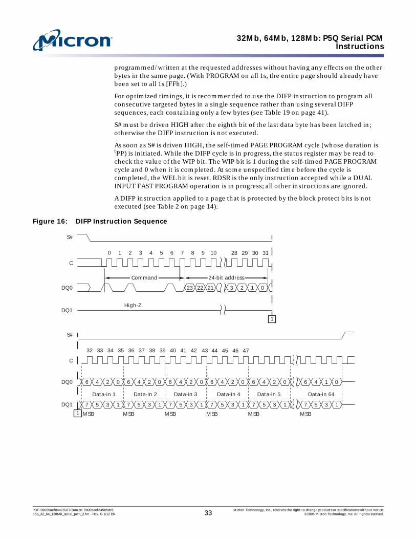
The DIFP instruction is entered by driving chip select (S#) LOW, followed by the instruc-tion code, three address bytes, and at least one data byte on serial data input (DQ0).
If the six least significant address bits (A[5:0]) are not all zero, all transmitted data that goes beyond the end of the current page are programmed from the start address of the same page (from the address whose six least significant bits (A[5:0]) are all zero). Chip select (S#) must be driven LOW for the entire duration of the sequence. The instruction sequence is shown in Figure 16 on page 33.
If more than 64 bytes are sent to the device, previously latched data are discarded and the last 64 data bytes are guaranteed to be programmed/written correctly within the same page. If fewer than 64 data bytes are sent to device, they are correctly
C
DQ0
S#
48 49 50 51
Data byte 2
MSB MSB
MSB MSB
MSB
52 53 54 55 2072
2072
2074
2075
2076
2077
2078
2079
40 41 42 43 44 45 46 47
Data byte 3
23 22 21 3 2 1 0 3 2 1 07 6 5 4
3 2 1 07 6 5 4
Data byte 64
3 2 1 07 6 5 43 2 1 07 6 5 4
C
DQ0
S#
21 3 4 5 6 7 8 9 10
Command
0 28 29 30 31 32 33 34 35 36 37 38 39
Data byte 124-bit addressnote 1
1
1
PDF: 09005aef8447d377/Source: 09005aef845b5cb5 Micron Technology, Inc., reserves the right to change products or specifications without notice.p5q_32_64_128Mb_serial_pcm_2.fm - Rev. G 1/12 EN 32 ©2005 Micron Technology, Inc. All rights reserved.
32Mb, 64Mb, 128Mb: P5Q Serial PCMInstructions
programmed/written at the requested addresses without having any effects on the other bytes in the same page. (With PROGRAM on all 1s, the entire page should already have been set to all 1s [FFh].)
For optimized timings, it is recommended to use the DIFP instruction to program all consecutive targeted bytes in a single sequence rather than using several DIFP sequences, each containing only a few bytes (see Table 19 on page 41).
S# must be driven HIGH after the eighth bit of the last data byte has been latched in; otherwise the DIFP instruction is not executed.
As soon as S# is driven HIGH, the self-timed PAGE PROGRAM cycle (whose duration is tPP) is initiated. While the DIFP cycle is in progress, the status register may be read to check the value of the WIP bit. The WIP bit is 1 during the self-timed PAGE PROGRAM cycle and 0 when it is completed. At some unspecified time before the cycle is completed, the WEL bit is reset. RDSR is the only instruction accepted while a DUAL INPUT FAST PROGRAM operation is in progress; all other instructions are ignored.
A DIFP instruction applied to a page that is protected by the block protect bits is not executed (see Table 2 on page 14).
Figure 16: DIFP Instruction Sequence
7 5 3 1 7 5 3 1
C
DQ0
S#
3433 35 36 37 38 39 40 41 42 4332
DQ1
Data-in 1
MSB MSBMSB MSB
44 45 46 47
Data-in 2 Data-in 3 Data-in 64
6 4 2 0 6 4 2 0 6 4 2 0 6 4 1 0
23 22 21 3 2 1 0
C
DQ0
S#
21 3 4 5 6 7 8 9 10
Command
0
DQ1High-Z
28 29 30 31
24-bit address
1
1
7 5 3 1 7 5 3 1
MSBMSB
Data-in 4 Data-in 5
6 4 2 0 6 4 2 0
7 5 3 1 7 5 3 1
PDF: 09005aef8447d377/Source: 09005aef845b5cb5 Micron Technology, Inc., reserves the right to change products or specifications without notice.p5q_32_64_128Mb_serial_pcm_2.fm - Rev. G 1/12 EN 33 ©2005 Micron Technology, Inc. All rights reserved.
32Mb, 64Mb, 128Mb: P5Q Serial PCMInstructions
QUAD INPUT FAST PROGRAM (QIFP)Note: The following description of QUAD INPUT FAST PROGRAM applies to all instances of
QUAD INPUT FAST PROGRAM, including legacy PROGRAM, bit-alterable WRITE, and PROGRAM on all 1s.
The QUAD INPUT FAST PROGRAM (QIFP) instruction is very similar to the PP instruc-tion, except that the data are entered on four pins (DQ0, DQ1, DQ2, and DQ3) instead of one. Inputting the data on four pins instead of one quadruples the data transfer band-width compared with using the PP instruction.
The QIFP instruction is entered by driving S# LOW, followed by the instruction code, three address bytes, and at least one data byte on DQ0.
If the six least significant address bits A[5:0] are not all zero, all transmitted data that goes beyond the end of the current page are programmed from the start address of the same page (from the address whose six least significant bits A[5:0] are all zero). S# must be driven LOW for the entire duration of the sequence. The instruction sequence is shown in Figure 17 on page 35.
If more than 64 bytes are sent to the device, previously latched data are discarded and the last 64 data bytes are guaranteed to be programmed correctly within the same page. If fewer than 64 data bytes are sent to device, they are correctly programmed at the requested addresses without having any effects on the other bytes in the same page. (With PROGRAM on all 1s, the entire page should already have been set to all 1s [FFh].)
For optimized timings, it is recommended to use the QIFP instruction to program all consecutive targeted bytes in a single sequence rather than o using several QIFP sequences each containing only a few bytes (see Table 19 on page 41).
S# must be driven HIGH after the eighth bit of the last data byte has been latched in; otherwise the QIFP instruction is not executed. As soon as S# is driven HIGH, the self-timed PAGE PROGRAM cycle (whose duration is tPP) is initiated. While the DIFP cycle is in progress, the status register may be read to check the value of the WIP bit. The WIP bit is 1 during the self-timed PAGE PROGRAM cycle and 0 when it is completed. At some unspecified time before the cycle is completed, the WEL bit is reset. RDSR is the only instruction accepted while a QUAD INPUT FAST PROGRAM operation is in progress; all other instructions are ignored.
A QIFP instruction applied to a page that is protected by the block protect bits is not executed (see Table 2 on page 14).
PDF: 09005aef8447d377/Source: 09005aef845b5cb5 Micron Technology, Inc., reserves the right to change products or specifications without notice.p5q_32_64_128Mb_serial_pcm_2.fm - Rev. G 1/12 EN 34 ©2005 Micron Technology, Inc. All rights reserved.

32Mb, 64Mb, 128Mb: P5Q Serial PCMInstructions
Figure 17: QIFP Instruction Sequence
Notes: 1. After 32h is recognized, W# and HOLD# functionality is automatically disabled.
SECTOR ERASE (SE)
The SECTOR ERASE (SE) instruction sets all bits that are inside the chosen sector to 1 (FFh). Before it can be accepted, a WREN instruction must previously have been executed. After the WREN instruction has been decoded, the device sets the WEL bit.
The SE instruction is entered by driving S# LOW, followed by the instruction code and three address bytes on DQ0. Any address inside the sector is a valid address for the SE instruction (see Table 5 on page 18). S# must be driven LOW for the entire duration of the sequence. The instruction sequence is shown in Figure 18 on page 35.
S# must be driven HIGH after the eighth bit of the last address byte has been latched in; otherwise the SE instruction is not executed. As soon as S# is driven HIGH, the self-timed SECTOR ERASE cycle (whose duration is tSE) is initiated. While the SECTOR ERASE cycle is in progress, the status register may be read to check the value of the WIP bit. The WIP bit is 1 during the self-timed SECTOR ERASE cycle and is 0 when it is completed. At some unspecified time before the cycle is completed, the WEL bit is reset. RDSR is the only instruction accepted while device is busy with ERASE operation; all other instructions are ignored.
An SE instruction applied to a page that is protected by the block protect bits is not executed (see Table 2 on page 14 and Table 5 on page 18).
Figure 18: SE Instruction Sequence
5 1 5 1
23 22 21 3 2 1 0
C
DQ0
S#
21 3 4 5 6 7 8 9 10
Command 32h
Don’t Care
Don’t Care
Don’t Care‘1’
0
DQ1
MSB MSB
32 33 34 35 3628 29 30 31
24-bit address
37 38 39 40 41 42 43
4 0 4 0
6 2 6 2DQ2
7 3 7 3
5 1 5 1
MSB MSB
Data-in 1
Data-in 2
Data-in 3
Data-in4
Data-in 5
Data-in6
4 0 4 0
6 2 6 2
7 3 7 3
5 1 5 1
MSB MSB
4 0 4 0
6 2 6 2
7 3 7 3DQ3
23 22 2 1 0
C
DQ1
S#
21 3 4 5 6 7 8 9
Command
0
MSB
29 30 31
24-bit addressnote 1
PDF: 09005aef8447d377/Source: 09005aef845b5cb5 Micron Technology, Inc., reserves the right to change products or specifications without notice.p5q_32_64_128Mb_serial_pcm_2.fm - Rev. G 1/12 EN 35 ©2005 Micron Technology, Inc. All rights reserved.
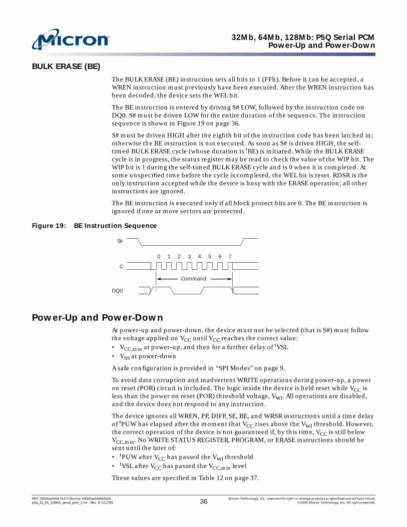
32Mb, 64Mb, 128Mb: P5Q Serial PCMPower-Up and Power-Down
BULK ERASE (BE)
The BULK ERASE (BE) instruction sets all bits to 1 (FFh). Before it can be accepted, a WREN instruction must previously have been executed. After the WREN instruction has been decoded, the device sets the WEL bit.
The BE instruction is entered by driving S# LOW, followed by the instruction code on DQ0. S# must be driven LOW for the entire duration of the sequence. The instruction sequence is shown in Figure 19 on page 36.
S# must be driven HIGH after the eighth bit of the instruction code has been latched in; otherwise the BE instruction is not executed. As soon as S# is driven HIGH, the self-timed BULK ERASE cycle (whose duration is tBE) is initiated. While the BULK ERASE cycle is in progress, the status register may be read to check the value of the WIP bit. The WIP bit is 1 during the self-timed BULK ERASE cycle and is 0 when it is completed. At some unspecified time before the cycle is completed, the WEL bit is reset. RDSR is the only instruction accepted while the device is busy with the ERASE operation; all other instructions are ignored.
The BE instruction is executed only if all block protect bits are 0. The BE instruction is ignored if one or more sectors are protected.
Figure 19: BE Instruction Sequence
Power-Up and Power-DownAt power-up and power-down, the device must not be selected (that is S#) must follow the voltage applied on VCC until VCC reaches the correct value: • VCC,min at power-up, and then for a further delay of tVSL• VSS at power-down
A safe configuration is provided in “SPI Modes” on page 9.
To avoid data corruption and inadvertent WRITE operations during power-up, a power on reset (POR) circuit is included. The logic inside the device is held reset while VCC is less than the power on reset (POR) threshold voltage, VWI. All operations are disabled, and the device does not respond to any instruction.
The device ignores all WREN, PP, DIFP, SE, BE, and WRSR instructions until a time delay of tPUW has elapsed after the moment that VCC rises above the VWI threshold. However, the correct operation of the device is not guaranteed if, by this time, VCC is still below VCC,min. No WRITE STATUS REGISTER, PROGRAM, or ERASE instructions should be sent until the later of:• tPUW after VCC has passed the VWI threshold• tVSL after VCC has passed the VCC,min level
These values are specified in Table 12 on page 37.
C
DQ0
S#
21 3 4 5 6 7
Command
0
PDF: 09005aef8447d377/Source: 09005aef845b5cb5 Micron Technology, Inc., reserves the right to change products or specifications without notice.p5q_32_64_128Mb_serial_pcm_2.fm - Rev. G 1/12 EN 36 ©2005 Micron Technology, Inc. All rights reserved.

32Mb, 64Mb, 128Mb: P5Q Serial PCMPower-Up and Power-Down
If the time, tVSL, has elapsed after VCC rises above VCC,min, the device can be selected for READ instructions even if the tPUW delay has not yet fully elapsed.
After power-up, the device is in the following states: • The device is in the standby power mode.• The WEL bit is reset.• The WIP bit is reset.
Normal precautions must be taken for supply line decoupling to stabilize the VCC supply. Each device in a system should have the VCC line decoupled by a suitable capacitor close to the package pins (generally, this capacitor is about 100nF).
At power-down when VCC drops from the operating voltage to below the power on reset (POR) threshold voltage, VWI, all operations are disabled and the device does not respond to any instruction (if power-down occurs while a WRITE, PROGRAM, or ERASE cycle is in progress, some data corruption may occur).
Figure 20: Power-Up Timing
Notes: 1. These parameters are characterized only.
Table 12: Power-Up Timing and VWI Threshold
Symbol Parameter Min Max UnittVSL
1 VCC,min to S# LOW 100 – µstPUW1 Time delay to write instruction 1 10 msVWI
1 Write inhibit voltage 1.5 2.5 V
VCC
VCC (MIN)
VWI
Reset stateof thedevice
Chip selection not allowed
PROGRAM, ERASE, and WRITE commands are rejected by the device
tVSL
tPUW
Time
Read access allowed Device fullyaccessible
VCC (MAX)
PDF: 09005aef8447d377/Source: 09005aef845b5cb5 Micron Technology, Inc., reserves the right to change products or specifications without notice.p5q_32_64_128Mb_serial_pcm_2.fm - Rev. G 1/12 EN 37 ©2005 Micron Technology, Inc. All rights reserved.

32Mb, 64Mb, 128Mb: P5Q Serial PCMInitial Delivery State
Initial Delivery StateThe device is delivered with the memory array erased: all bits are set to 1 (each byte contains FFh). The status register contains 00h (all status register bits are 0).
Maximum RatingsStresses greater than those listed in Table 13 may cause permanent damage to the device. This is a stress rating only, and functional operation of the device at these or any other conditions outside those indicated in the operational sections of this specification is not implied. Exposure to absolute maximum rating conditions for extended periods may adversely affect reliability.
Notes: 1. JEDEC Standard JESD22-A114A (C1 = 100pF; R1 = 1500Ω; R2 = 500Ω).
DC and AC CharacteristicsThe parameters in the DC and AC characteristics are derived from tests performed under the measurement conditions summarized in the relevant tables. Operating condi-tions in device circuits must match the measurement conditions when relying on the quoted parameters.
Operating Conditions
Notes: 1. Data retention for Micron PCM is 10 years at 70°C. For additional documentation about data retention, contact your local Micron sales representative.
2. Temperature range applies to 128Mb parts only.
Endurance Specifications
Notes: 1. A WRITE cycle is defined as any time a bit changes within a 32-byte page.
Table 13: Absolute Maximum RatingsNote 1 applies to the entire table
Symbol Parameter Min Max Unit
VIO Input and output voltage (with respect to ground) –0.6 VCC + 0.6 VVCC Supply voltage –0.6 4.0 VVESD Electrostatic discharge voltage (human body model)1 –2000 2000 V
Table 14: Operating Conditions
Symbol Parameter Min Typ Max Unit
VCC Supply voltage 2.7 – 3.6 VTA Ambient operating temperature (66 MHz)2 0 – 70 °CTA Ambient operating temperature (33 MHz) –40 – 85 °C
Table 15: Endurance Specifications
Parameter Condition Min Units Notes
WRITE cycle Main block 1,000,000 Cycles per32-byte page
1
Parameter block 1,000,000
PDF: 09005aef8447d377/Source: 09005aef845b5cb5 Micron Technology, Inc., reserves the right to change products or specifications without notice.p5q_32_64_128Mb_serial_pcm_2.fm - Rev. G 1/12 EN 38 ©2005 Micron Technology, Inc. All rights reserved.

32Mb, 64Mb, 128Mb: P5Q Serial PCMDC and AC Characteristics
AC Measurement Conditions
Figure 21: AC Measurement I/O Waveform
Capacitance
Notes: 1. Sampled only, not 100% tested, at TA = 25°C and a frequency of 33 MHz.
Table 16: AC Measurement Conditions
Symbol Parameter Min Max Unit
CL Load capacitance 30 30 pF
Input rise and fall times – 5 ns
Input pulse voltages 0.2–0.8 VCC V
Input timing reference voltages 0.3–0.7 VCC V
Output timing reference voltages VCC/2 V
Table 17: Capacitance1
Symbol Parameter Test Condition Min Max Unit
CIN/OUT Input/output capacitance (DQ0/DQ1) VOUT = 0V – 8 pFCIN Input capacitance (other pins) VIN = 0V – 6 pF
Input and outputtiming reference levelsInput levels
0.8VCC
0.2VCC
0.7VCC
0.3VCC
0.5VCC
PDF: 09005aef8447d377/Source: 09005aef845b5cb5 Micron Technology, Inc., reserves the right to change products or specifications without notice.p5q_32_64_128Mb_serial_pcm_2.fm - Rev. G 1/12 EN 39 ©2005 Micron Technology, Inc. All rights reserved.

32Mb, 64Mb, 128Mb: P5Q Serial PCMDC and AC Characteristics
DC Characteristics
Notes: 1. For additional test conditions, refer to Table 14 on page 38.
Table 18: DC Characteristics
Symbol Parameter Test Condition1 Min Max Unit
ILI Input leakage current – ±2 µAILO Output leakage current – ±2 µAICC1 Standby current S# = VCC, VIN = VSS or VCC – 200 µAICC3 Operating current (READ) C = 0.1VCC /0.9VCC at 66 MHz,
DQ1 = open– 16 mA
C = 0.1VCC /0.9VCC at 33 MHz, DQ1 = open
– 7 mA
Operating current (DOFR) C = 0.1VCC /0.9VCC at 66 MHz, DQ0 = DQ1 = open
– 20 mA
Operating current (QOFR) C = 0.1VCC /0.9VCC at 50 MHz, DQ0 = DQ1 = DQ2 = DQ3 = open
– 24 mA
ICC4 Operating current (PP) S# = VCC – 50 mA
Operating current (DIFP) S#= VCC – 50 mA
Operating current (QIFP) S# = VCC – 50 mAICC5 Operating current (WRSR) S# = VCC – 50 mAICC6 Operating current (SE, BE) S# = VCC – 50 mAVIL Input low voltage – 0.5 0.3 VCC VVIH Input high voltage 0.7 VCC VCC + 0.4 VVOL Output low voltage IOL = 1.6mA – 0.4 VVOH Output high voltage IOH = –100µA VCC - 0.2 V
PDF: 09005aef8447d377/Source: 09005aef845b5cb5 Micron Technology, Inc., reserves the right to change products or specifications without notice.p5q_32_64_128Mb_serial_pcm_2.fm - Rev. G 1/12 EN 40 ©2005 Micron Technology, Inc. All rights reserved.
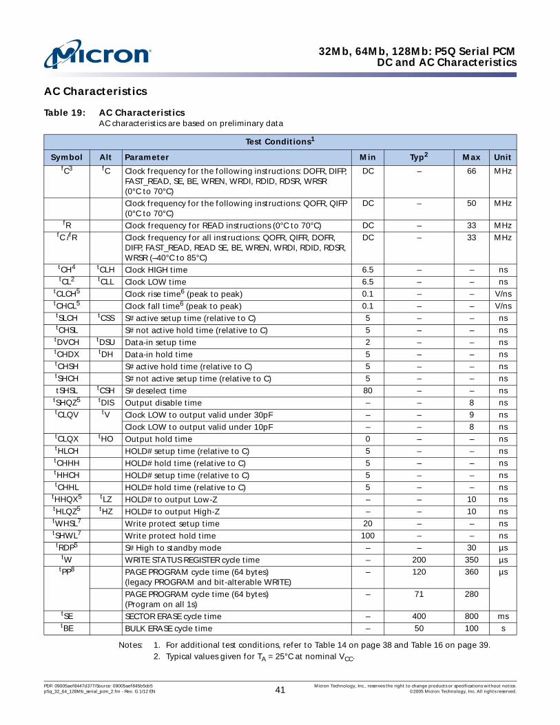
32Mb, 64Mb, 128Mb: P5Q Serial PCMDC and AC Characteristics
AC Characteristics
Notes: 1. For additional test conditions, refer to Table 14 on page 38 and Table 16 on page 39.2. Typical values given for TA = 25°C at nominal VCC.
Table 19: AC CharacteristicsAC characteristics are based on preliminary data
Test Conditions1
Symbol Alt Parameter Min Typ2 Max UnitfC3 fC Clock frequency for the following instructions: DOFR, DIFP,
FAST_READ, SE, BE, WREN, WRDI, RDID, RDSR, WRSR(0°C to 70°C)
DC – 66 MHz
Clock frequency for the following instructions: QOFR, QIFP (0°C to 70°C)
DC – 50 MHz
fR Clock frequency for READ instructions (0°C to 70°C) DC – 33 MHzfC /fR Clock frequency for all instructions: QOFR, QIFR, DOFR,
DIFP, FAST_READ, READ SE, BE, WREN, WRDI, RDID, RDSR, WRSR (–40°C to 85°C)
DC – 33 MHz
tCH4 tCLH Clock HIGH time 6.5 – – nstCL2 tCLL Clock LOW time 6.5 – – ns
tCLCH5 Clock rise time6 (peak to peak) 0.1 – – V/nstCHCL5 Clock fall time6 (peak to peak) 0.1 – – V/nstSLCH tCSS S# active setup time (relative to C) 5 – – nstCHSL S# not active hold time (relative to C) 5 – – nstDVCH tDSU Data-in setup time 2 – – nstCHDX tDH Data-in hold time 5 – – nstCHSH S# active hold time (relative to C) 5 – – nstSHCH S# not active setup time (relative to C) 5 – – nstSHSL tCSH S# deselect time 80 – – ns
tSHQZ5 tDIS Output disable time – – 8 nstCLQV tV Clock LOW to output valid under 30pF – – 9 ns
Clock LOW to output valid under 10pF – – 8 nstCLQX tHO Output hold time 0 – – nstHLCH HOLD# setup time (relative to C) 5 – – nstCHHH HOLD# hold time (relative to C) 5 – – nstHHCH HOLD# setup time (relative to C) 5 – – nstCHHL HOLD# hold time (relative to C) 5 – – ns
tHHQX5 tLZ HOLD# to output Low-Z – – 10 nstHLQZ5 tHZ HOLD# to output High-Z – – 10 nstWHSL7 Write protect setup time 20 – – nstSHWL7 Write protect hold time 100 – – nstRDP5 S# High to standby mode – – 30 µs
tW WRITE STATUS REGISTER cycle time – 200 350 µstPP8 PAGE PROGRAM cycle time (64 bytes)
(legacy PROGRAM and bit-alterable WRITE)– 120 360 µs
PAGE PROGRAM cycle time (64 bytes)(Program on all 1s)
– 71 280
tSE SECTOR ERASE cycle time – 400 800 mstBE BULK ERASE cycle time – 50 100 s
PDF: 09005aef8447d377/Source: 09005aef845b5cb5 Micron Technology, Inc., reserves the right to change products or specifications without notice.p5q_32_64_128Mb_serial_pcm_2.fm - Rev. G 1/12 EN 41 ©2005 Micron Technology, Inc. All rights reserved.

32Mb, 64Mb, 128Mb: P5Q Serial PCMDC and AC Characteristics
3. Temperature range applies to 128Mb parts only.4. tCH + tCL must be ≥ 1/fC.5. Value guaranteed by characterization, not 100% tested in production.6. Expressed as a slew rate.7. Only applicable as a constraint for a WRSR instruction when SRWD is set to 1.8. When using the PP instruction to program consecutive bytes, optimized timings are
obtained with one sequence, including all the bytes versus several sequences of only a few bytes (1 ≤ n ≤ 64).
Figure 22: Serial Input Timing
Figure 23: Write Protect Setup and Hold Timing During WRSR when SRWD = 1
tSLCHtCHSL
tDVCH tCHDX tCLCHtCHCL
tCHSH tSHCH
tSHSL
S#
C
DQ0
DQ1 High-Z High-Z
MSB in LSB in
High-Z
W#
S#
C
DQ0
DQ1
tWHSL tSHWL
PDF: 09005aef8447d377/Source: 09005aef845b5cb5 Micron Technology, Inc., reserves the right to change products or specifications without notice.p5q_32_64_128Mb_serial_pcm_2.fm - Rev. G 1/12 EN 42 ©2005 Micron Technology, Inc. All rights reserved.
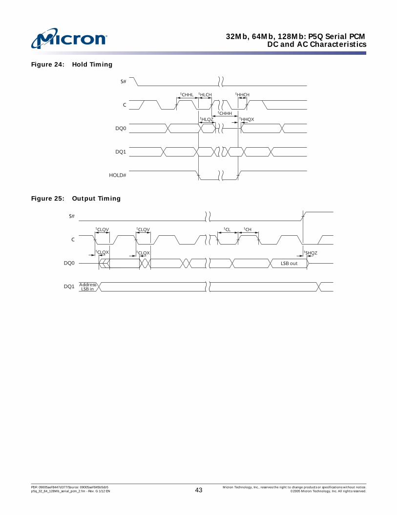
32Mb, 64Mb, 128Mb: P5Q Serial PCMDC and AC Characteristics
Figure 24: Hold Timing
Figure 25: Output Timing
tHLCHtCHHL tHHCH
tHLQZ
tCHHHtHHQX
S#
C
DQ0
DQ1
HOLD#
tCL tCH
S#
C
DQ0
DQ1
LSB out
AddressLSB in
tCLQX tCLQX tSHQZ
tCLQV tCLQV
PDF: 09005aef8447d377/Source: 09005aef845b5cb5 Micron Technology, Inc., reserves the right to change products or specifications without notice.p5q_32_64_128Mb_serial_pcm_2.fm - Rev. G 1/12 EN 43 ©2005 Micron Technology, Inc. All rights reserved.
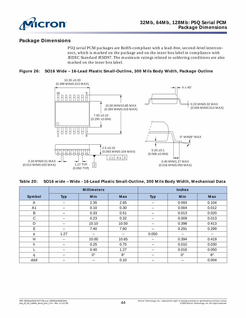
32Mb, 64Mb, 128Mb: P5Q Serial PCMPackage Dimensions
Package DimensionsP5Q serial PCM packages are RoHS-compliant with a lead-free, second-level intercon-nect, which is marked on the package and on the inner box label in compliance with JEDEC Standard JESD97. The maximum ratings related to soldering conditions are also marked on the inner box label.
Figure 26: SO16 Wide – 16-Lead Plastic Small-Outline, 300 Mils Body Width, Package Outline
Table 20: SO16 wide – Wide - 16-Lead Plastic Small-Outline, 300 Mils Body Width, Mechanical Data
Symbol
Millimeters Inches
Typ Min Max Typ Min Max
A – 2.35 2.65 – 0.093 0.104A1 – 0.10 0.30 – 0.004 0.012B – 0.33 0.51 – 0.013 0.020C – 0.23 0.32 – 0.009 0.013D – 10.10 10.50 – 0.398 0.413E – 7.40 7.60 – 0.291 0.299e 1.27 – – 0.050 – –H – 10.00 10.65 – 0.394 0.419h – 0.25 0.75 – 0.010 0.030L – 0.40 1.27 – 0.016 0.050q – 0° 8° – 0° 8°
ddd – – 0.10 – – 0.004
16
0.23 MIN/0.32 MAX(0.009 MIN/0.013 MAX)
1 8
9
0.40 MIN/1.27 MAX(0.016 MIN/0.050 MAX)
0.20 ±0.1(0.008 ±0.004)
2.5 ±0.15(0.093 MIN/0.104 MAX)
10.30 ±0.20(0.398 MIN/0.413 MAX)
7.50 ±0.10(0.295 ±0.004)
10.00 MIN/10.65 MAX(0.394 MIN/0.419 MAX)
0.33 MIN/0.51 MAX(0.013 MIN/0.020 MAX)
0.1 Z
0° MIN/8° MAX
1.27 TYP(0.050 TYP)
h x 45°
Z
PDF: 09005aef8447d377/Source: 09005aef845b5cb5 Micron Technology, Inc., reserves the right to change products or specifications without notice.p5q_32_64_128Mb_serial_pcm_2.fm - Rev. G 1/12 EN 44 ©2005 Micron Technology, Inc. All rights reserved.

32Mb, 64Mb, 128Mb: P5Q Serial PCMOrdering Information
Ordering Information
Table 21: Active Line Item Ordering Table
Part Number Description
NP5Q032AE3ESFC0E 32Mb 3V, SOIC, Pb-free,10.34 x 10.34 x 2.54, 16-lead (–40°C to 85°C)NP5Q064AE3ESFC0E 64Mb 3V, SOIC, Pb-free,10.34 x 10.34 x 2.54, 16-lead (–40°C to 85°C)NP5Q128AE3ESFC0E 128Mb 3V, SOIC, Pb-free,10.34 x 10.34 x 2.54, 16-lead (–40°C to 85°C)NP5Q128A13ESFC0E 128Mb 3V, SOIC, Pb-free,10.34 x 10.34 x 2.54, 16-lead (0°C to 70°C)
PDF: 09005aef8447d377/Source: 09005aef845b5cb5 Micron Technology, Inc., reserves the right to change products or specifications without notice.p5q_32_64_128Mb_serial_pcm_2.fm - Rev. G 1/12 EN 45 ©2005 Micron Technology, Inc. All rights reserved.

8000 S. Federal Way, P.O. Box 6, Boise, ID 83707-0006, Tel: 208-368-3900www.micron.com/productsupport Customer Comment Line: 800-932-4992
Micron and the Micron logo are trademarks of Micron Technology, Inc. All other trademarks are the property of their respective owners.This data sheet contains minimum and maximum limits specified over the power supply and temperature range set forth herein. Although
considered final, these specifications are subject to change, as further product development and data characterization sometimes occur.
32Mb, 64Mb, 128Mb: P5Q Serial PCMRevision History
PDF: 09005aef8447d377/Source: 09005aef845b5cb5 Micron Technology, Inc., reserves the right to change products or specifications without notice.p5q_32_64_128Mb_serial_pcm_rev_history.fm - Rev. G 1/12 EN 46 ©2005 Micron Technology, Inc. All rights reserved.
Revision History
Rev. G, Production . . . . . . . . . . . . . . . . . . . . . . . . . . . . . . . . . . . . . . . . . . . . . . . . . . . . . . . . . . . . . . . . . . . . . . . . . . . . . . . . . . . 1/12• Added 32Mb and 64Mb densities
Rev. F, Production . . . . . . . . . . . . . . . . . . . . . . . . . . . . . . . . . . . . . . . . . . . . . . . . . . . . . . . . . . . . . . . . . . . . . . . . . . . . . . . . . . .11/11• Changed –30°C to –40°C in features on first page, operating conditions table, AC char-
acteristics table, and active line item ordering table• Added temperature bullet in features with commercial and industrial temperatures
and corresponding frequencies
Rev. E, Production. . . . . . . . . . . . . . . . . . . . . . . . . . . . . . . . . . . . . . . . . . . . . . . . . . . . . . . . . . . . . . . . . . . . . . . . . . . . . . . . . . .03/11• Rebranded for Micron
Rev. D, Production . . . . . . . . . . . . . . . . . . . . . . . . . . . . . . . . . . . . . . . . . . . . . . . . . . . . . . . . . . . . . . . . . . . . . . . . . . . . . . . . . .07/10• Revised cover page with –30°C to +85°C• Revised read current at 33MHz (Table 14)• Revised AC characteristics for –30°C to +85°C (Table 15)• Revised ordering information
Rev. C, Production . . . . . . . . . . . . . . . . . . . . . . . . . . . . . . . . . . . . . . . . . . . . . . . . . . . . . . . . . . . . . . . . . . . . . . . . . . . . . . . . . .04/10• Added Numonyx product branding• Added endurance verbiage (Table 11)• Revised DC and AC section: tVSL (MIN), tCLQV (MAX), tHLQZ (MAX), Page Program
(TYP/MAX), Sector Erase (TYP/MAX), Bulk Erase (MAX)
Rev. B, Production . . . . . . . . . . . . . . . . . . . . . . . . . . . . . . . . . . . . . . . . . . . . . . . . . . . . . . . . . . . . . . . . . . . . . . . . . . . . . . . . . .08/09• Removed Numonyx Confidential• Added figures 23 and 24• Revised Hold Condition verbiage• Removed Streaming Mode from data sheet• Added P5Q product designator
Rev. A, Production. . . . . . . . . . . . . . . . . . . . . . . . . . . . . . . . . . . . . . . . . . . . . . . . . . . . . . . . . . . . . . . . . . . . . . . . . . . . . . . . . . .06/09• Initial release