P3MD Labs - Purdue Department of Physics and Astronomy: Home · 2012-01-22 · P3MD has excellent...
17
P3MD Labs Introduction to the facilities of the Purdue Experimental Particle Physics research groups
Transcript of P3MD Labs - Purdue Department of Physics and Astronomy: Home · 2012-01-22 · P3MD has excellent...

P3MD Labs
Introduction to the facilities of the Purdue Experimental Particle Physics research groups

Purdue Particle Physics Microstructure Development Laboratories
2
Cleanrooms • 3000 sq. ft. of clean
rooms in 3 labs • Temperature and
humidity control • ESD protection
Presenter
Presentation Notes
P3MD has excellent equipment for instrumentation. The labs are fully equipped with data acquisition systems. The class 10,000 space has stand-alone air handling and filtering providing temperature control to ±1ºC and control of relative humidity to ±5%. ESD protection equipment through-out the labs.

Purdue Particle Physics Microstructure Development Laboratories
3
Coordinate Measuring Machine
• Assembly alignment and surveying are done using an optical probe on our Mitutoyo Coordinate Measuring Machine
• Dimensional inspections of fixtures and detector mechanics are done using a touch probe on the CMM
Presenter
Presentation Notes
Mitutoyo Bright 710 CMM with a general purpose software program: range: 700mm x 1000mm x 600mm (28” x 40” x 24”) resolution: 0.5 um Length measuring accuracy: (3+3L/1000)um, where L = measuring length in mm repeatability: 4 um For example, the uncertainty when measuring across a LSST Raft (130mm x 130mm) is <3.4 microns. In practice, the repeatability of our CMM measurements (established by calibration tests) is within 1.5 microns. The Purdue CMM meets the accuracy requirements for probe measurements of features on LSST Sensor module, Raft and Tower structures.

Semi-automated module assembly station
• Developing a robotic ‘pick-and-place’ machine for module assembly
• Gantry positioning system integrated with vision, pattern recognition, vacuum tools, adhesive dispenser, electro-valves and sensors
• Demonstrations of ‘pick-and-place’ pixel module assembly posted on YouTube
Purdue Particle Physics Microstructure Development Laboratories
4
Presenter
Presentation Notes
Aerotech AGS15000 Linear Motor Gantry Positioning System and ADRS-150 Rotary Stage EFD Ultimus V liquid dispensing controller LabVIEW programmable Reliable and repeatable semi-automatic assembly Extensive use of student labor for: Development of tooling and procedures Large part of production modules assembled by students

Purdue Particle Physics Microstructure Development Laboratories
5
Wire bonding
• 2 automated ultrasonic wire bonding machines
• Wire bond pull tester for quality control
Presenter
Presentation Notes
2 automated ultrasonic wirebonding machines F&K Delvotec 6400 semi-automatic wirebond machine K&S 1478 semi-automatic wirebond machine Routine wirebond pull tests for quality control (all bonds >5 gram pull-strength) Uni-Tek wirebond pull tester Plasma Etch cleans hybrid bonding surfaces to enhance wirebond pull strength Plasma-Preen Plasma etcher/cleaner >1 million wire bonds on CLEO and CMS silicon and hybrids

Flip Chip Bonding
• High accuracy bonder for aligning, placing and reworking flip chip and ball grid array modules
Purdue Particle Physics Microstructure Development Laboratories
6
Presenter
Presentation Notes
Non negligible number of assembled flip-chip modules (10-15%) fail due to damaged components and/or many bad interconnection. The JFP Model PP5-6 Universal Flip-Chip Bonder is a versatile micro-assembly aligner, placer, rework station for failed chip removal and replacement. The JFP PP5-6 consists of a high-resolution vision alignment system to ensure micron placement accuracy, an open platform and modular design for a high level of flexibility to accommodate a wide range of applications, hands-off substrate handling with bonding force control, and real-time process and thermal control, monitoring and recording.

Purdue Particle Physics Microstructure Development Laboratories
7
Processing equipment • Optical inspection stations • Vacuum oven • Microwave plasma etcher • Environmental chamber • Encapsulation station • Dry cabinet storage
Shared equipment on campus including: • Mask design, mask & detector fabrication • SEM, Scanning Auger spectroscopy • Ion Beam cutting, Reactive Ion Etcher • Dicing saws • Ribbon and Ball Wire bonders • Profilometer, Ellipsometer, Tensile tester
Presenter
Presentation Notes
Nikon Optiphot 66 measuring microscope and high magnification semi-conductor inspection microscope Multiple inspection stereoscopes Blue M vacuum oven Plasma-Preen Plasma etcher/cleaner Tenney Benchmaster Temp. & Humidity Environmental Test Chamber I & J 2300N robotic encapsulation station

Purdue Particle Physics Microstructure Development Laboratories
8
Custom Design
• CAD modeling for assembly and testing fixtures
• Design and engineering of detector mechanics
• Expert Purdue machine shops for fabrication

Purdue Particle Physics Microstructure Development Laboratories
9
Probe Stations • 2 probe stations for device
characterization, design and module de-bug, failure analysis
• Thermal chuck (-65°C to 200°C)
Presenter
Presentation Notes
Two semi-automatic probe stations: Cascade Microtech Summit 12K with environmental chamber, thermal chuck (-50C to +200C) and probe card holder Alessi with semi-automatic visual inspection (image capturing and processing)

Purdue Particle Physics Microstructure Development Laboratories
10
Sensor Development and Testing
• Computer simulation of sensor performance
• DC characterization • Charge collection efficiency • Irradiation and aging
studies
1.50E+03
1.60E+03
1.70E+03
1.80E+03
1.90E+03
2.00E+03
2.10E+03
-150 -100 -50 0 50 100 150
distance [um]
Pixe
l Raw
out
put [
AD
C]
Al SiO2 p+ n+
22 um
Presenter
Presentation Notes
Since the early 90’s, the Purdue group has been developing silicon sensors for major HEP experiments. Large contribution in CDF microstrips and CMS Pixels. The group has demonstrated capabilities in: Innovative ideas and applications Complete development of silicon sensors Conceptual design Simulations Layout Prototyping Production (with commercial manufacturers) Quality control We have new R&D commitments in future projects: rad-hard SLHC upgrades for CMS ILC silicon tracker

Purdue Particle Physics Microstructure Development Laboratories
11
Module electrical test station
• Test setup: – IR LED – IR Pulsed Laser – XYZ-axis motion – Thermoelectric cooling
Dark Box
Logic Analyzer
DAQ
Laser optics
Pixel detector module
Laser beam spot
10 um
Presenter
Presentation Notes
Module characterization station with IR Pulsed Laser, XYZ-axis motion, Thermoelectric cooling.

Purdue Particle Physics Microstructure Development Laboratories
12
Experience
• Design: CDF Run II Sensors, CMS-FPix sensors • Fabrication: CLEO III SVX & CMS-FPix plaquettes • Installation & Commissioning: CLEO III SVX, CDF
Run II SVX & L00, CMS FPix • R&D: Si pixel/strip & MPGD for SLHC and ILC • Year-round research experience for undergraduate &
graduate student instrumentation PhDs.
Presenter
Presentation Notes
P3MD has successfully met many mechanical challenges, including: Precision alignment of components Evaluation of optimal materials and fabrication for detector support structures Engineering and design of mechanical and thermal solutions for detector structures and cooling Development of tools, procedures and quality controls for reliable detector assembly Our group has a well establish expertise on sensor R&D, testing and implementation of silicon particle detectors for HEP experiments. Our group led the construction of the pixels for the CMS experiment and gained strong experience with flip-chip assembly. Fantastic contributions from graduate and undergraduate students. Previous and present projects (CDF, CLEO, CMS and now LSST) have been successfully completed providing innovative tools to the scientific community. Our expertise can contribute to the development and construction of the CMS FPIX Upgrade detector, LSST camera and other projects.

Forward Pixel Disk ~3 million pixels
1x3 Plaquette
CMS Forward Pixel Detector Purdue will assemble and test
~1000 Plaquettes Pixel Sensors bump bonded to
Read Out Chips Very High Density Interconnects
Laser
Plaquette
~0.5 million wire bonds in FPix detector
ROCs
VHDI
Pixel Sensor
Plaquette
Pulsed IR laser scanning
Presenter
Presentation Notes
A Blade is made of 2 Panels with Plaquettes of 7 different geometries. A total of 45 ROCs (Read-Out Chips) per Blade bump-bonded to 5 different size Pixel Sensors. 4 full Disks 16 cooling loops 96 Blades 192 Panels 672 Plaquettes

Purdue leads mechanical & thermal design work
• Design for accurate and stable mount for sensors and electronics in the Camera
• Assembly sequence & insertion tooling
• Mechanical & Thermal analysis (FEA & prototype tests)
• risk & cost analysis
• Also contribute to design of overall Camera (Harvard, LLNL, BNL, Penn, Purdue and SLAC)
LSST Instrumentation: Purdue is design & fabrication site for the Corner Rafts of LSST Camera
CCD test station
CCD Guide Sensor
A challenging project 146 million pixels/corner
DARK BOX TURBO
VACUUM PUMP
UNIVERSAL CRYOGENICS DEWAR
Presenter
Presentation Notes
4 Wavefront sensors on focal plane array observe stars Sensor data used to move active optics Input to PSF determination for later image analysis Practical implementation of this is shown here Each CCD is a science sensor split in 2 an offset along the optical axis by +/-1.5 mm 8 Guide sensors (same as Science CCD sensors) shown here is a sample Science CCD installed in a Dewar Note guiding is done at 9 Hz High frequency piece fed directly to the servo motor to minimize jitter The low frequency piece will be sent to telescope control system to determine the appropriate offset and correction for mount axes and camera rotator

CLEO III Silicon Vertex Detector
Purdue responsibilities: • Mechanical design and
engineering • Assembly of silicon strip
ladders using CVD diamond for support, wire bonding, module testing
• Kinematic mounting of ladders on end cones
• Cooling system • Transportation to Cornell,
SVX installation into CLEO
Presenter
Presentation Notes
Si3 Mechanical Challenges Silicon Ladders Outer layer 53.3 cm long – one of the longest ladders constructed for a collider geometry Precision assembly of wafers over length <15 micron Natural frequency >100HZ and self deflection <25 micron CTE match between support beam and silicon Electrical compatibility between support beam and silicon Beam geometry Several considered (side rails, vertical strip, tubes, V-beam) A closed geometry was chosen to provide torsional stiffness. The V-beam geometry is easily constructed from sheet materials and makes use of the stiffness of the silicon which closes the triangular beam section. Beam material Many materials (Be, SiC, carbon fiber & Kevlar composites) evaluated for stiffness, radiation length and CTE match to silicon CVD diamond was a clear winner for CTE and stiffness, as well as being an electrical insulator and excellent thermal conductor. Conical end supports Precision location of ladders to <25 microns Mounting locations for hybrid electronics and cables Thermal management of hybrids (500 watts) Kinematic mounting Isolate ladders from end supports to mitigate forces due to external loads (i.e. transport) or thermal changes
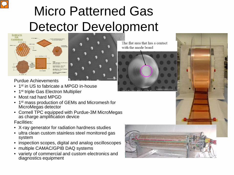
Micro Patterned Gas Detector Development
Purdue Achievements • 1st in US to fabricate a MPGD in-house • 1st triple Gas Electron Multiplier • Most rad hard MPGD • 1st mass production of GEMs and Micromesh for
MicroMegas detector • Cornell TPC equipped with Purdue-3M MicroMegas
as charge amplification device Facilities: • X-ray generator for radiation hardness studies • ultra clean custom stainless steel monitored gas
system • inspection scopes, digital and analog oscilloscopes • multiple CAMAC/GPIB DAQ systems • variety of commercial and custom electronics and
diagnostics equipment
Presenter
Presentation Notes
Rigaku X-ray generator

Purdue Particle Physics Microstructure Development Laboratories
17
Camera for Whipple Observatory
• Designed and managed the fabrication and assembly of an upgrade camera for the Whipple Observatory 10M Telescope.
• The camera was upgraded from the previous 331 pixel camera to a finer resolution 490 pixel camera comprising 379 half-inch and 111 one-inch Photo Multiplier Tubes.
• Each PMT mounted in a spring-loaded, ¼-turn fitting allowing in-situ replacement of individual PMT’s in the camera
• Focal plane (front face of PMT’s) flat to 50 microns