P-N JUNCTION DIODE CHARACTERISTICS AIM · Experiment No: 2 ZENER DIODE CHARACTERISTICS AIM: 1. To...
69
Experiment No: 1 P-N JUNCTION DIODE CHARACTERISTICS AIM: 1. To plot Volt-Ampere Characteristics of Silicon P-N Junction Diode. 2. To find cut-in Voltage for Silicon P-N Junction diode. 3. To find static and dynamic resistances in both forward and reverse biased conditions for Si P-N Junction diode. Components: Equipment: Name Range Qty Bread Board Regulated Power Supply Digital Ammeter Digital Voltmeter Connecting Wires - 0-30V DC 0-200A/20mA 0-2V/20V DC 1 1 1 1 Theory: Donor impurities (pentavalent) are introduced into one-side and acceptor impurities into the other side of a single crystal of an intrinsic semiconductor to form a p-n diode with a Junction called depletion region (this region is depleted off the charge carriers). This Region gives rise to a potential barrier V called Cut- in Voltage. This is the voltage across the diode at which it starts conducting. It can conduct beyond this Potential. The P-N junction supports uni-directional current flow. If +ve terminal of the input supply is connected to anode (P-side) and –ve terminal of the input supply is connected to cathode (N- side) then diode is said to be forward biased. In this condition the height of the potential barrier at the junction is lowered by an amount equal to given forward biasing voltage. Both the holes from p-side and electrons from n-side cross the junction simultaneously and constitute a forward current (injected minority current – due to holes crossing the junction and entering N-side of the diode, due to electrons crossing the junction and entering P-side of the diode). Assuming current flowing through the diode to be very large, the diode can be approximated as short-circuited switch. If –ve terminal of the input supply is connected to anode (p-side) and +ve terminal of the input supply is connected to cathode (n-side) then the diode is said to be reverse biased. In Name Qty Diodes IN 4007(Si) Resistor 1K, 10K 1 1
Transcript of P-N JUNCTION DIODE CHARACTERISTICS AIM · Experiment No: 2 ZENER DIODE CHARACTERISTICS AIM: 1. To...

Experiment No: 1
P-N JUNCTION DIODE CHARACTERISTICS
AIM:
1. To plot Volt-Ampere Characteristics of Silicon P-N Junction Diode.
2. To find cut-in Voltage for Silicon P-N Junction diode.
3. To find static and dynamic resistances in both forward and reverse biased conditions
for Si P-N Junction diode.
Components:
Equipment:
Name Range Qty
Bread Board
Regulated Power
Supply
Digital Ammeter
Digital Voltmeter
Connecting Wires
-
0-30V DC
0-200A/20mA
0-2V/20V DC
1
1
1
1
Theory:
Donor impurities (pentavalent) are introduced into one-side and acceptor impurities
into the other side of a single crystal of an intrinsic semiconductor to form a p-n diode with a
Junction called depletion region (this region is depleted off the charge carriers). This Region
gives rise to a potential barrier V called Cut- in Voltage. This is the voltage across the diode
at which it starts conducting. It can conduct beyond this Potential.
The P-N junction supports uni-directional current flow. If +ve terminal of the input supply is
connected to anode (P-side) and –ve terminal of the input supply is connected to cathode
(N- side) then diode is said to be forward biased. In this condition the height of the potential
barrier at the junction is lowered by an amount equal to given forward biasing voltage. Both
the holes from p-side and electrons from n-side cross the junction simultaneously and
constitute a forward current (injected minority current – due to holes crossing the junction
and entering N-side of the diode, due to electrons crossing the junction and entering P-side of
the diode). Assuming current flowing through the diode to be very large, the diode can be
approximated as short-circuited switch.
If –ve terminal of the input supply is connected to anode (p-side) and +ve terminal of the
input supply is connected to cathode (n-side) then the diode is said to be reverse biased. In
Name Qty
Diodes IN 4007(Si)
Resistor 1K, 10K
1
1
this condition an amount equal to reverse biasing voltage increases the height of the potential
barrier at the junction. Both the holes on p-side and electrons on n-side tend to move away
from the junction thereby increasing the depleted region. However the process cannot
continue indefinitely, thus a small current called reverse saturation current continues to flow
in the diode. This small current is due to thermally generated carriers. Assuming current
flowing through the diode to be negligible, the diode can be approximated as an open
circuited switch.
The volt-ampere characteristics of a diode explained by following equation:
I =I0 (ev/(v
T) - 1) where
I=current flowing in the diode I0=reverse saturation current
V=voltage applied to the diode
VT=volt-equivalent of temperature=kT/q=T/11,600=26mV (@ room temp).
=1 (for Ge) and 2 (for Si)
It is observed that Ge diode has smaller cut-in-voltage when compared to Si diode. The
reverse saturation current in Ge diode is larger in magnitude when compared to silicon diode.
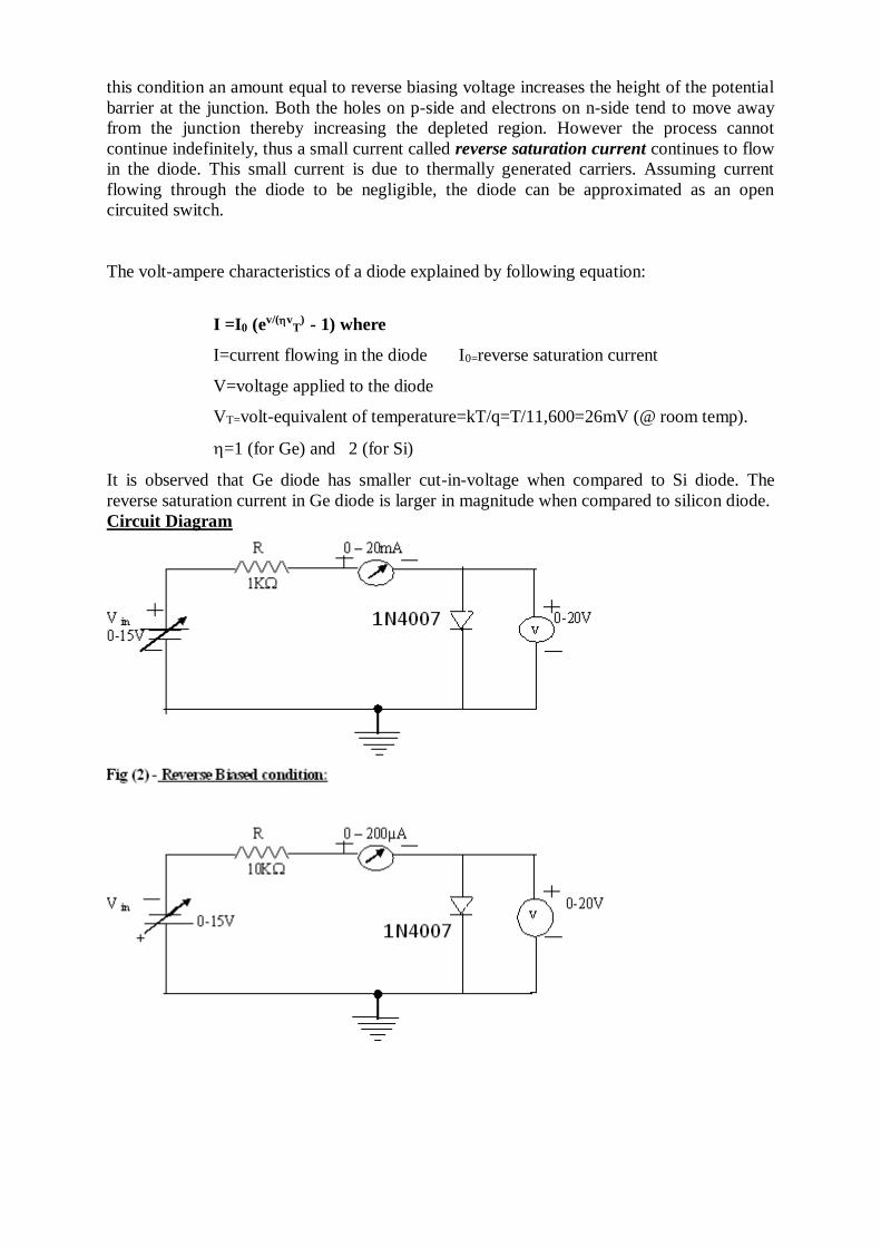
Circuit Diagram

Procedure:
Forward Biased Condition:
1. Connect the circuit as shown in figure (1) using silicon PN Junction diode.
2. Vary Vf gradually in steps of 0.1 volts upto 5volts and note down the corresponding
readings of If .
3. Step Size is not fixed because of non linear curve and vary the X-axis variable (i.e. if
output variation is more, decrease input step size and vice versa).
4. Tabulate different forward currents obtained for different forward voltages.
Reverse biased condition:
1. Connect the circuit as shown in figure (2) using silicon PN Junction diode.
2. Vary Vr gradually in steps of 0.5 volts upto 8 volts and note down the corresponding
readings of Ir.
3. Tabulate different reverse currents obtained for different reverse voltages. (Ir = VR /
R, where VR is the Voltage across 10K Resistor).
Observations
Si diode in forward biased conditions:
Sl.
No RPS
Voltage
Forward
Voltage across
the diode
Vf (volts)
Forward
current
through the
diode If (mA)
Si diode in reverse biased conditions:
Graph (Instructions):
1. Take a graph sheet and divide it into 4 equal parts. Mark origin at the center of the
graph sheet.
2. Now mark + ve x-axis as Vf
- Ve x-axis as Vr
+ Ve y-axis as If
- ve y-axis as Ir.
3. Mark the readings tabulated for Si forward biased condition in first Quadrant and Si
reverse biased condition in third Quadrant.
Calculations from Graph:
If (mA)
Vr (volts) Vf(volts)
Ir (A)
Static forward Resistance R dc = V f / If Ω
Dynamic forward Resistance r ac = V f /If Ω
Static Reverse Resistance R dc =V r / I r Ω
Sl. No RPS Voltage
Reverse Voltage
across the diode
Vr (volts)
Reverse
current
through the
diode Ir (A)

Dynamic Reverse Resistance r ac = V r /I r Ω
Precautions:
1. While doing the experiment do not exceed the ratings of the diode. This may lead to
damage the diode.
2. Connect voltmeter and Ammeter in correct polarities as shown in the circuit diagram.
3. Do not switch ON the power supply unless you have checked the circuit connections
as per the circuit diagram.
Result:
1. Cut in voltage = ……… V
2. Static forward resistance = ……….
3. Dynamic forward resistance = ……….
VIVA-VOCEQuestions
1. How depletion region is formed in the PN junction?
2. What are trivalent and pentavalent impurities?
3. What is cut-in or knee voltage? Specify its value in case of Ge or Si?
4. What is maximum forward current and maximum reverse voltage? What is it
required?
5. What is leakage current?
6. How does PN-junction diode acts as a switch?
7. What is the effect of temperature in the diode reverse characteristics?
8. What is break down voltage?
9. What is incremental resistance of a diode?
10. What is diode equation?
11. What is the value of VT in the diode equation?
12. Explain the dynamic resistance of a diode?
13. Explain the phenomenon of breakdown in PN- diode?
14. What is an ideal diode? How does it differ from a real diode?
15. What are the specifications of a diode?
16. Temperature co-efficient of resistance of
(i) Metals (ii) Intrinsic semiconductor (iii) Extrinsic semiconductor
(iv) FET (v) BJT
17. What is the internal impedance of
(i) Ideal current source (ii) Ideal voltage source (iii) Ammeter
Specifications:
For Silicon Diode IN 4007: -
Max. Forward Current = 1A
Max. Reverse Current = 30A
Max. Forward Voltage = 0.8V
Max. Reverse Voltage = 1000V
Max. Power dissipation = 30mw
Temperature = - 65 to 2000C

Experiment No: 2
ZENER DIODE CHARACTERISTICS
AIM:
1. To plot Volt-Ampere characteristics of Zener diode.
2. To find Zener break down voltage in reverse biased condition.
3. To calculate static and dynamic resistances of the Zener diode in both forward and
reverse biased conditions (before, after break down voltages).
Components:
Equipment:
Name Range
Breadboard
Regulated DC power supply
Ammeter
Voltmeter
Connecting Wires
-
0-30V
0-20mA
0-20V
Specifications:
Breakdown Voltage = 5.1V
Power dissipation = 0.75W
Max. Forward Current = 1A
Theory:
An ideal P-N Junction diode does not conduct in reverse biased condition. A zener diode
Conducts excellently even in reverse biased condition. These diodes operate at a precise
Value of voltage called break down voltage.
A zener diode when forward biased behaves like an ordinary P-N junction diode.
A zener diode when reverse biased can either undergo avalanche break down or zener
break down.
Avalanche break down:-If both p-side and n-side of the diode are lightly doped, depletion
region at the junction widens. Application of a very large electric field at the junction may
Name Qty
Zener Diode
Resistor 1K
1
1

rupture covalent bonding between electrons. Such rupture leads to the generation of a large
number of charge carriers resulting in avalanche multiplication.
Zener breaks down:-If both p-side and n-side of the diode are heavily doped, depletion
region at the junction reduces. Application of even a small voltage at the junction ruptures
covalent bonding and generates large number of charge carriers. Such sudden increase in the
number of charge carriers results in zener mechanism.
Circuit Diagram:
Fig (1) – Forward Bias Condition:
R Izf (0 – 20) mA
1K
Vin V zf (0-3)V
0-30V
Fig (2) – Reverse Bias Condition:
R Izr (0 – 20) mA
1K
Vin Vzr (0-20) V
0-30V
Procedure:
Forward biased condition:
1. Connect the circuit as shown in fig (1).
2. Vary Vzf gradually steps of 0.1 volts up to 5volts and note down the corresponding
readings of Izf.
3. Tabulate different forward currents obtained for different forward voltages.
Reverse biased condition:
V
V

1. Connect the circuit as shown in fig (2).
2. Vary Vzr gradually in steps of 0.5 volts up to 8 volts and note down the corresponding
readings of Izr.
3. Tabulate different reverse currents obtained for different reverse voltages.
Observations:
Si diode in forward biased conditions:
diode in reverse biased conditions:
VOLTAGE REGULATION:
Sl.No RPS Voltage
Forward Voltage
across the diode
Vzf (volts)
Forward current
through the
diode Izf (mA)
Sl.No RPS
Voltage
Reverse
Voltage across
the diode Vzr
(volts)
Reverse current
through the
diode Izr (mA)

LOAD REGULATION CHARACTERISTICS:
1. Connect the Circuit as per the Circuit Diagram on the bread board. 2. By changing the load Resistance, kept constant I/P Voltage at 5V, 10 V, 15 V as
per table given below. Take the readings of O/P Voltmeter (Vo=Vz). 3. Now by changing the I/P Voltage, kept constant load Resistance at 1K, 2K, 3K
as per table given below. Take the readings of O/P Voltmeter (Vo=Vz).
Vi (V)
RL1=1K RL2=2K
VO (V) VO (V)
0 1
3
5
7
9
11
13
15
20
S.No RL ()
Vi1= 5V Vi2= 10V
VO (V) VO (V)
1 100 2 300
3 500
4 700
5 900
6 1K
7 3K
8 5K
9 7K
10 10K
Department of ECE,MIST
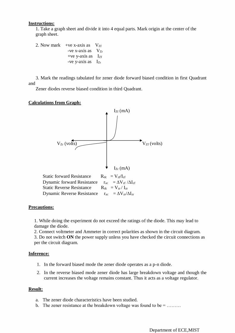
Instructions:
1. Take a graph sheet and divide it into 4 equal parts. Mark origin at the center of the
graph sheet.
2. Now mark +ve x-axis as VZf
-ve x-axis as VZr
+ve y-axis as IZf
-ve y-axis as IZr
3. Mark the readings tabulated for zener diode forward biased condition in first Quadrant
and
Zener diodes reverse biased condition in third Quadrant.
Calculations from Graph:
IZf (mA)
VZr (volts) VZf (volts)
IZr (mA)
Static forward Resistance Rdc = Vzf/Izf
Dynamic forward Resistance rac = Vzf /Izf
Static Reverse Resistance Rdc = Vzr / Izr
Dynamic Reverse Resistance rac = Vzr/Izr
Precautions:
1. While doing the experiment do not exceed the ratings of the diode. This may lead to
damage the diode.
2. Connect voltmeter and Ammeter in correct polarities as shown in the circuit diagram.
3. Do not switch ON the power supply unless you have checked the circuit connections as
per the circuit diagram.
Inference:
1. In the forward biased mode the zener diode operates as a p-n diode.
2. In the reverse biased mode zener diode has large breakdown voltage and though the
current increases the voltage remains constant. Thus it acts as a voltage regulator.
Result:
a. The zener diode characteristics have been studied.
b. The zener resistance at the breakdown voltage was found to be = ………

Department of ECE,MIST
VIVA-VOCE Questions
1. What is a zener diode? How it differs from an ordinary diode?
2. Explain the concept of zener breakdown?
3. What is avalanche breakdown?
4. What type of biasing must be used when a zener diode is used as a regulator?
5. Current in a 1W – 10V zener diode must be limited to a maximum of what value?
6. What are the advantages of zener diode?
7. State reason why an ordinary diode suffers avalanche breakdown rather than zener
breakdown?
8. If impurities in a zener diode increases what happens to the forward voltage?
9. Can zener be used as a rectifier?
10. Specifications of the zener diode?
Department of ECE,MIST
Experiment No: 3
COMMON BASE CONFIGURATION
AIM: To study the input and output characteristics of a transistor in common base
configuration.
Components:
Equipment:
Name Range Qty
Bread Board
Regulated Power Supply
Digital Ammeter
Digital Voltmeter
Connecting Wires
-
0-30V DC
0-20mA
0-20V DC
1
2
2
2
Specifications:
For Transistor CL 100S: -
Max. Collector Current = 0.1A
VCEO max = 50V
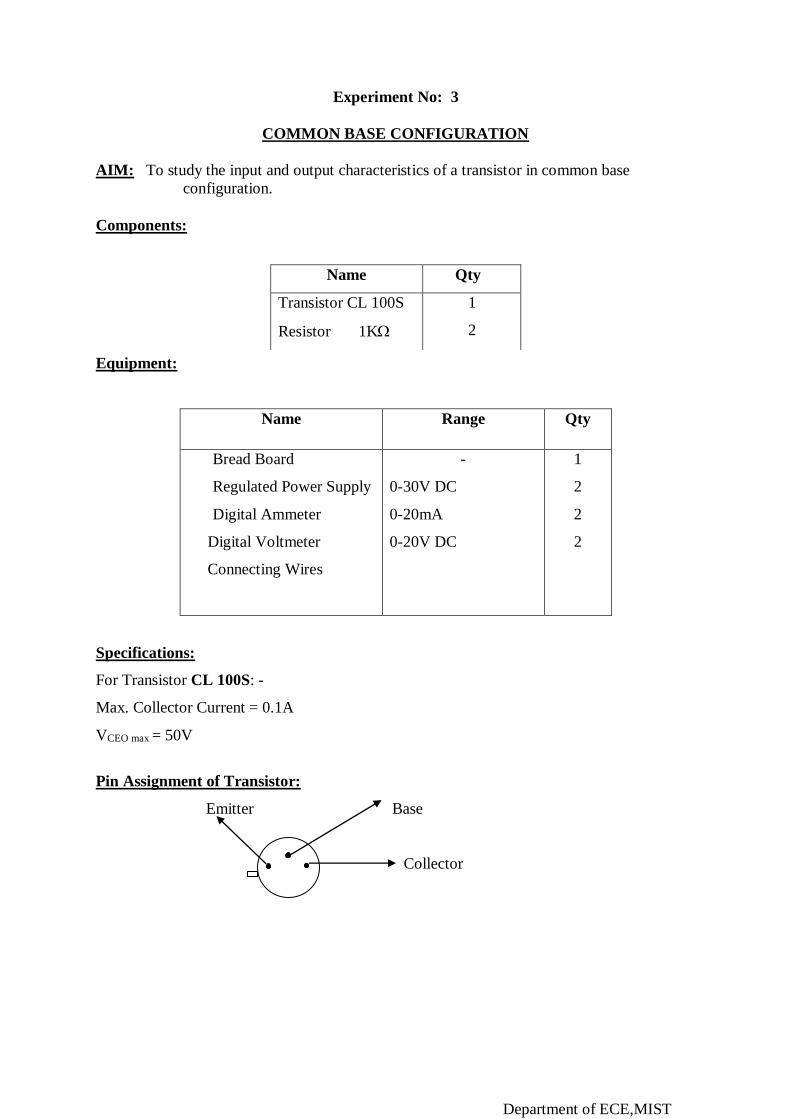
Pin Assignment of Transistor:
Emitter Base
Collector
Name Qty
Transistor CL 100S
Resistor 1K
1
2
Department of ECE,MIST
Circuit Diagram:
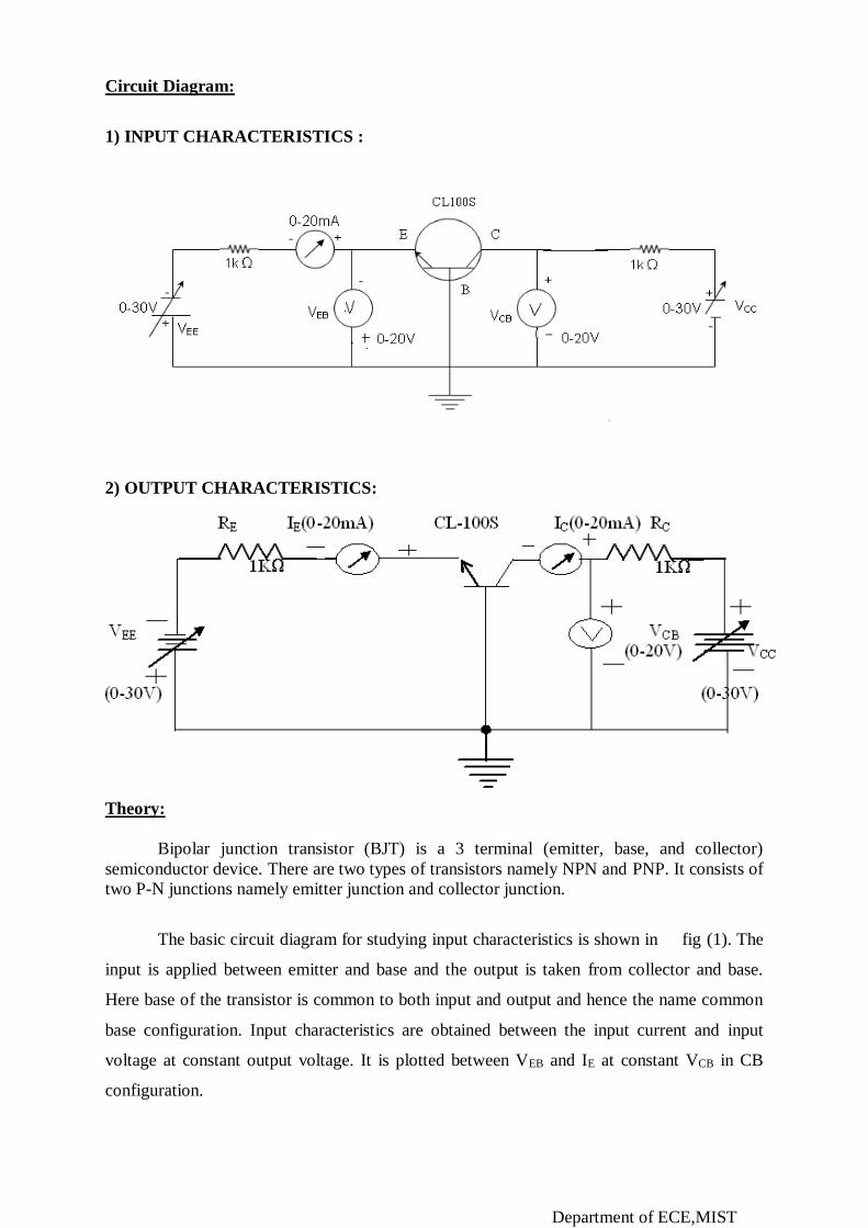
1) INPUT CHARACTERISTICS :
2) OUTPUT CHARACTERISTICS:
Theory:
Bipolar junction transistor (BJT) is a 3 terminal (emitter, base, and collector)
semiconductor device. There are two types of transistors namely NPN and PNP. It consists of
two P-N junctions namely emitter junction and collector junction.
The basic circuit diagram for studying input characteristics is shown in fig (1). The
input is applied between emitter and base and the output is taken from collector and base.
Here base of the transistor is common to both input and output and hence the name common
base configuration. Input characteristics are obtained between the input current and input
voltage at constant output voltage. It is plotted between VEB and IE at constant VCB in CB
configuration.

Department of ECE,MIST
Output characteristics are obtained between the output voltage and output Current keeping
input current constant. It is plotted between VCB and IC at Constant IE in CB configuration.
Procedure:
Input Characteristics
1. Make connections as per circuit diagram fig (1).
2. Keep output voltage VCB = 0V by varying VEE
3. Varying VEE gradually, note down both emitter current IE and emitter-base voltage
(VEB).
4. Repeat above procedure (step 3) for VCB =5V.
Output Characteristics
1. Make connections as per circuit diagram fig (2).
2. By varying VEE keep the emitter current I E = 5mA.
3. Varying VCC gradually, note down the readings of collector-current (IC) and collector-
base voltage (VCB).
4. Repeat above procedure (step 3) for IE = 10mA.
Observations:
VCB = 0 V VCB = 5 V
IE
(mA)
VEB
(V)
IE
(mA)
VEB
(V)
IE = 5mA IE = 10mA
VCB
(V)
IC
(mA)
VCB
(V)
IC
(mA)
Department of ECE,MIST
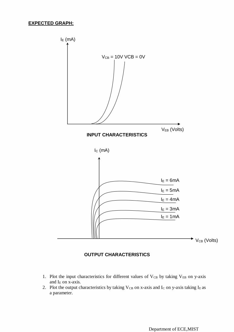
EXPECTED GRAPH:
INPUT CHARACTERISTICS
OUTPUT CHARACTERISTICS
1. Plot the input characteristics for different values of VCB by taking VEB on y-axis
and IE on x-axis.
2. Plot the output characteristics by taking VCB on x-axis and IC on y-axis taking IE as
a parameter.
VCB = 10V VCB = 0V
VEB (Volts)
IE (mA)
VCB (Volts)
IC (mA)
IE = 6mA
IE = 5mA
IE = 4mA
IE = 3mA
IE = 1mA

Department of ECE,MIST
Calculations from graph:
1. Input resistance: To obtain input resistance find VEB and IE for a constant VCB on
one of the input characteristics.
Ri = VEB / IE ( VCB = constant)
2. Output resistance: To obtain output resistance find Ic and VCB at constant IE.
Ro = VCB / IC (IE = constant).
Inference:
1. Input resistance is in the order of tens of ohms since emitter-base junction is
forward biased.
2. Output resistance is in the order of hundreds of kilo-ohms since collector-base
junction is reverse biased.
3. Higher is the value of VCB, smaller is the cut in voltage.
4. Increase in the value of IB causes saturation of transistor at small voltages.
Precautions:
1. While doing the experiment do not exceed the ratings of the
Transistor. This may lead to damage the transistor.
2. Connect voltmeter and Ammeter in correct polarities as shown in the
Circuit diagram.
3. Do not switch ON the power supply unless you have checked the
Circuit connections as per the circuit diagram.
4. Make sure while selecting the emitter, base and collector terminals of
The transistor.
Result:
1. Input Resistance (Ri) = ……………
2. Output Resistance (Ro) = ……………
3. =Ic/Ie |vce=constant ______
1. How to test the diode & transistor-using multimeter?
2. What are the uses of a common base configuration?
3. What is a buffer?
4. Why CB configuration is called constant current source?
5. What is the maximum value of ‘‘?
6. Draw the symbol of NPN and PnP transistors?
7. What is base-width modulation?
8. Why is base made thin?
9. What is the significance of arrow in the transistor symbol?
10. Define current amplification factor?
VIVA-VOCE Questions

Department of ECE,MIST
11. Compare input and output impedance of CB configuration with that of CC
configuration?
12. What is the function of a transistor?
13. Define? What is the range of?
14. Why CC configuration is called as emitter follower?

Department of ECE,MIST
Experiment No: 4
COMMON EMITTER CONFIGURATION
AIM: To study the input and output characteristics of a transistor
In common emitter configuration.
Components:
Equipment:
Name Range Qty
Bread Board
Regulated Power
Supply
Digital Ammeter
Digital Voltmeter
Connecting Wires
-
0-30V DC
0-20mA /0-200A
0-2V/20V DC
1
2
1
1
Specifications:
For Transistor CL 100S: -
Max. Collector Current = 0.1A
VCEO max = 50V
Pin assignment of Transistor:
Emitter Base
Collector
Name Qty
Transistor CL 100S
Resistor 220K
Resistor 560
1
1
1

Department of ECE,MIST
Circuit Diagram:
1) INPUT CHARACTERISTICS
RC 1K
RB 100K IB (0-200A)
CL-100S
(0-20V)
VBB VBE VCE
(0-20V) VCC
0-30V 0-30V
2) OUTPUT CHARACTERISTICS: (0-20mA) RC 1k
RB IB (0-200A)
IC
100K CL-100S
VBB VCE
VCC
(0-30v) (0-20V) (0-30) v
Theory: The basic circuit diagram for studying input and output characteristics are
shown in fig (1) & fig (2). In this the input is applied between base and emitter
and the output is taken from collector and emitter. Here emitter is common to
both input and output and hence the name common emitter configuration.
Input characteristics are obtained between the input current and input voltage
taking output voltage as parameter. It is plotted between VBE and IB at constant
VCE in CE configuration.
Output characteristics are obtained between the output voltage and output
current taking input current as parameter. It is plotted between VCE and IC at
constant IB in CE configuration.
Procedure:
Input Characteristics
4. Make the connections as per circuit diagram fig (1).

Department of ECE,MIST
5. Keep output voltage VCE = 0V by varying VCC.
6. Varying VBB gradually, note down both base current IB and base - emitter voltage
(VBE).
4. Repeat above procedure (step 3) for VCE =5V.
Output Characteristics
5. Make the connections as per circuit diagram fig (2).
6. By varying VBB keep the base current I B = 20A.
7. Varying VCC gradually, note down the readings of collector-current (IC) and collector-
emitter voltage (VCE).
8. Repeat above procedure (step 3) for IE=40A.
Observations:
I
Input Characteristics Output Characteristics
VCE = 0 V VCE = 5 V
IB
(A)
VBE
(V)
IB
(A)
VBE
(V)
IB= 20A IB = 40A
VCE
(V)
IC (mA) VCE
(V)
IC
(mA)

Department of ECE,MIST
Expected graph:
3. Plot the input
characteristics by taking VBE on Y-axis and IB on X-axis at constant VCE.
4. Plot the output characteristics by taking VCE on Y-axis and IC on X-axis by
taking IB as a parameter.
Calculations from graph:
2. Input resistance: To obtain input resistance find VBE and IB at constant VCE on
one of the input characteristics.
Then Ri = VBE / IB (VCE constant)
2. Output resistance: To obtain output resistance, find IC and VCE at
Constant IB.
Ro = VCE / IC (IB constant)
Inference:
1. Medium Input and Output resistances.
2. Smaller value of VCE comes earlier cut-in-voltage.
3. Increase in the value of IB causes saturation of the transistor at an
Earlier voltage.
Precautions:
4. While doing the experiment do not exceed the ratings of the
Transistor. This may lead to damage the transistor.
5. Connect voltmeter and Ammeter in correct polarities as shown in the
Circuit diagram.
6. Do not switch ON the power supply unless you have checked the
Circuit connections as per the circuit diagram.
7. Make sure while selecting the emitter, base and collector terminals of
the transistor.
Result:
1. Input Resistance (Ri) = ……………
Input Characteristics and output Characteristics:

Department of ECE,MIST
2. Output Resistance (Ro) = ……………
3. β=Ic/IB |vce=constant ______
Viva-VoceQuestions
1. Two discrete diodes connected back-to-back cannot work as a transistor, why?
2. For amplification, CE configuration is preferred, why?
3. To operate a transistor as amplifier, the emitter junction is forward biased and the
collector junction is reversed biased, why?
4. With the rise in temperature, the leakage collector current increases, why?
5. An electronic device transistor is named as transistor, why?
6. Most of the transistor are NPN type and not PnP, why?
7. The forward resistance of emitter junction is slightly less than forward resistance of
collector junction, why?

Department of ECE,MIST
= Im sint 0 t
= 0 t 2
Experiment No: 5
HALF WAVE RECTIFIER WITH & WITHOUT FILTERS
AIM: Study of Half – wave rectifier with & without Filter and to finds Ripple Factor.
EQUIPMENT:
Name Range Quantity
Transformer
Bread Board
Digital Multimeter
Resistor
Connecting wires
9-0-9V/12-0-12V
1kΩ,10kΩ
1
1
1
1
THEORY:
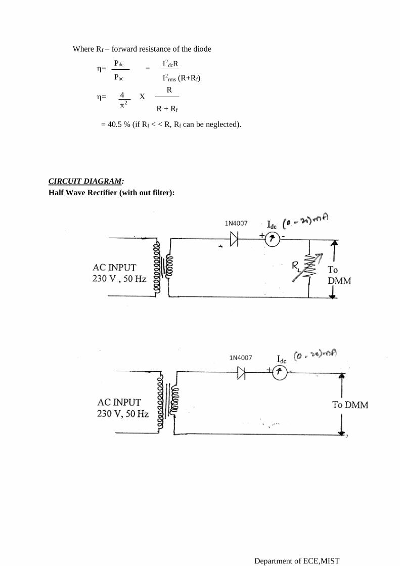
Consider the given circuit. Assume the diode to be ideal i.e. Vf = 0, Rr =, Rs = 0. During
the positive half cycle, the diode is forward biased and it conducts and hence a current flows
through the load resistor. During the negative half cycle, the diode is reverse biased and it is
equivalent to an open circuit, hence the current through the load resistance is zero. Thus the
diode conducts only for one half cycle and results in a half wave rectified output.
MATHEMATICAL ANALYSIS
(Neglecting Rf and Rs)
Let Vac = Vm sint is the input AC signal, the current Iac flows only for one half cycle i.e.
from t = 0 to t = , where as it is zero for the duration
T 2
Therefore, Iac = Vac/R = Vm Sinwt/R
Where Im = maximum value of current
Vm = maximum value of voltage
AVERAGE OR DC VALUE OF CURRENT
2
Idc = 1/2 Im (sint) dt
0
The conversion of AC into DC is called Rectification. Electronic devices can convert AC
power into DC power with high efficiency

Department of ECE,MIST
= 1 Im2
2 2 dt =
0 1-cos2t
2
Im
2
Vrms = Vm
2
V ac
V dc
2
Idc =1/2 sint dt + 0 dt = Im /
0
Similarly
Vdc = Vm /
The RMS VALUE OF CURRENT
Similarly
RIPPLE FACTOR:
The output of a half – wave rectifier consists of some undesirable ac components known as
ripple. These can be removed using suitable filter circuits.
Ripple factor is defined as the ratio of the effective value of AC components to the average
DC value. It is denoted by the symbol
=
V2rms = V2
ac + V2dc
= V2rms - V
2dc
V dc
Converting V rms and Vdc into its corresponding Vm value, we get
= 1.21
RECTIFICATION FACTOR:
The ratio of output DC power to the input AC power is defined as efficiency
Output power = I2dcR
Input power = I2rms(R+Rf)
Irms = 1 1 2
2 2 Iac2 dt
0
= 1 1 2
2 2 Im2 sin 2dt
0
Department of ECE,MIST
R
R + Rf
Where Rf – forward resistance of the diode
= =
= X
= 40.5 % (if Rf < < R, Rf can be neglected).
CIRCUIT DIAGRAM:
Half Wave Rectifier (with out filter):
Pdc
Pac
I2dcR
I2rms (R+Rf)
4
2

Department of ECE,MIST
Half Wave Rectifier (with C-filter):
PROCEDURE:
1. Make connections as per the Circuit Diagram.
2. Note down the AC and DC Voltages and Currents without Filter and with Load.
3. And again observe the AC and DC Voltages and Currents with L & Filters and
with load.
4. Observe the Voltage across the secondary of the Transformer.
Tabular Column:
Vac = _____ (Voltage across the secondary of the transformer)
Condition Vac Vdc Vm R
Without Filter
Condition Vac Vdc Vm C R
With C Filter
Department of ECE,MIST
Vac
Vdc
CALCULATIONS:
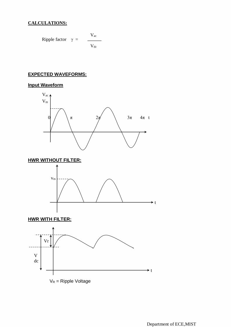
Ripple factor =
EXPECTED WAVEFORMS: Input Waveform HWR WITHOUT FILTER:
HWR WITH FILTER:
Vac
Vm
0 π 2π 3π 4π t
vm
t
V
dc
t
Vr
VR = Ripple Voltage

Department of ECE,MIST
RESULT: -
Parameters Without
filter
With c - Filter
Ripple Factor
Efficiency
VIVA-VOCE Questions
1. Why are rectifiers used with a filter at their output?
2. What is the voltage regulation of the rectifier?
3. What is the ideal value of regulation?
4. What does no load condition refer to?
5. What are the advantages of bridge rectifier?
6. What are the advantages and disadvantages of capacitor filter?
7. What are the applications of rectifiers?
8. What is the regulation for a
(i) Half - wave circuit (ii) Full-wave circuit
9. What is PIV? State it value in case of (i) Half wave (ii) Full wave (iii) Bridge
rectifier.
10. What is the output signal frequency in case of (i) Half wave (ii) Full wave (iii) Bridge
rectifier?

Department of ECE,MIST
Experiment No: 6
FULLWAVE RECTIFIER WITH & WITHOUT FILTERS
AIM: To Study the Full – wave rectifier Circuit & to Find its, Ripple factor
EQUIPMENT:
Name Range Quantity
Transformer
Bread Board
Digital Multimeter
Resistor
Connecting wires
9-0-9V/12-0-12V
1kΩ,10kΩ
1
1
1
1
THEORY:
FULL-WAVE RECTIFIER:
The full-wave rectifier consists of a center-tap transformer, which results in equal
voltages above and below the center-tap. During the positive half cycle, a positive voltage
appears at the anode of D1 while a negative voltage appears at the anode of D2. Due to this
diode D1 is forward biased it results in a current Id1 through the load R.
During the negative half cycle, a positive voltage appears at the anode of D2 and
hence it is forward biased. Resulting in a current Id2 through the load at the same instant a
negative voltage appears at the anode of D1 thus reverse biasing it and hence it doesn’t
conduct.
MATHEMATICAL ANALYSIS (Neglecting Rf and Rs)
Therefore, I = Id1 + Id2
t sin V V m ac
The conversion of AC into DC is called Rectification. Electronic devices can convert
AC power into DC power with high efficiency
The current through the load during both half cycles is in the same direction and hence it is
the sum of the individual currents and is unidirectional

Department of ECE,MIST
2πωt 0
πωt0 t sinR
V I m
d1
2πωt t sinR
V-
πωt0 0 I
m
d2
AVERAGE OR DC VALUE OF CURRENT Idc
2
Idc =1/2 Im (sint) dt - Im (sint) dt = 2 Im /
0
Similarly,
Vdc = 2Vm /
The RMS VALUE OF CURRENT
= 2
Im
Similarly, 2
V V m
rms
RIPPLE FACTOR
dc
ac
V
V
( = 0.48)
RECTIFICATION FACTOR
The ratio of output DC power to the input AC power is defined as efficiency
Efficiency,
The individual currents and voltages are combined in the load and there fore their average
values are double that obtained in a half – wave rectifier circuit.
Ripple factor is defined as the ratio of the effective value of AC components to the
average DC value. It is denoted by the symbol
= 1 1 2
2 2 Im2 sin 2 t dt
0

Department of ECE,MIST
100 * I IV
I * V
P
P
2
dc
2
acrms
dcdc
ac
dc
= 81% (if R >> Rf . then Rf can be neglected)
Where Rf – forward resistance of two diode
Peak – Inverse – Voltage (PIV)
It is the maximum voltage that has to be with stood by a diode when it is reverse biased
PIV = 2Vm
Advantages of Full wave Rectifier
1. is reduced
2. is improved
Disadvantages of Full wave Rectifier
1. Output voltage is half the secondary voltage
2. Diodes with high PIV rating are used
Manufacturing of center-taped transformer is quite expensive and so Full wave rectifier with
center-taped transformer is costly.
CIRCUIT DIAGRAM (With out Filter):
(With C -Filter) :

Department of ECE,MIST
VNL – VFL
VFL
PROCEDURE:
5. Make connections as per the Circuit Diagram.
6. Note down the AC and DC Voltages and Currents without Filter and with Load.
7. And again observe the AC and DC Voltages and Currents with Filter and with load.
8. Observe the Voltage across the secondary of the Transformer (i.e. Vrms).
Tabular Column:
Condition Vac Vdc Vm R
Without Filter
Condition Vac Vdc Vm C R
With C Filter
CALCULATIONS:
Ripple factor =
Efficiency 100 * I IV
I * V
P
P
2
dc
2
acrms
dcdc
ac
dc
Percentage of regulation = X 100 %
VNL = Voltage across load resistance,
When minimum current flows though it
VFL = Voltage across load resistance, When maximum current flows through it.
Vac
Vdc

Department of ECE,MIST
EXPECTED WAVEFORMS: Input Waveform FULLWAVE RECTIFIER WITHOUT FILTER:
FULLWAVE RECTIFIER WITH FILTER:
t
Vac
Vm
0 π 2π 3π 4π t
Vac
Vm
0 π 2π 3π
4π
VR = Ripple Voltage
vd
c
t
vr

Department of ECE,MIST
RESULT:
Parameters Without
filter
With C Filter
Ripple Factor
Efficiency
VIVA-VOCE Questions
1. A diode should not be employed in the circuits where it is to carry more than its
maximum forward current, why?
2. While selecting a diode, the most important consideration is its PIV, why?
3. The rectifier diodes are never operated in the breakdown region, why?
4. In filter circuits, a capacitor is always connected in parallel, why?
In filter circuits, an inductor is always connected in series why?

Department of ECE,MIST
Experiment No: 7
FET CHARACTERISTICS
AIM: To study Drain Characteristics and Transfer Characteristics of a FET.
Components:
Name Qty
JFET BFW 10 1
Resistors 470 2
Equipment:
Name Range Qty
FET Trainer Kit
Digital Ammeter Digital Voltmeter
Connecting Wires
-
0-20mA
0-20 V
1
1
2
Specifications:
For JFET BFW10: -
Gate Source Voltage VGS = - 30V
Forward Gain Current IGF = 10 mA
Maximum Power Dissipation PD = 300 mW.
Circuit Diagram:
ID (0–20mA) 1k
68K G D
BFW10
S VDD
VGG VGS VDS
(0-30V) (0–20V)
(0–20V)

Department of ECE,MIST
Pin assignment of FET:
Source Drain
Gate
Substrate
Theory:
The basic circuit diagram for studying drain and transfer characteristics is
Shown in figure.
Drain characteristics are obtained between the drain to source voltage (VDS) and drain current
(ID) taking gate to source voltage (VGS) as the parameter.
Transfer characteristics are obtained between the gate to source voltage (VGS) and Drain
current (ID) taking drain to source voltage (VDS) as parameter.
Procedure:
DRAIN CHARACTERISTICS
1. Make the connections as per circuit diagram.
2. Keep VGS = 0V by varying VGG.
3. Varying VDD gradually, note down both drain current ID and drain to source voltage
(VDS).
4. Repeat above procedure (step 3) for VGS = -1V.
TRANSFER CHARACTERISTICS:
1. Keep VDS = 2V by varying VDD.
2. Varying VGG gradually from 0 – 5V, note down both drain current (ID) and gate to
source voltage (VGS).
3. Repeat above procedure (step 2) for VDS = 4V.
Observations:
DRAIN CHARACTERISTICS:
VGS = 0V VGS = -1V
VDS (V) ID (mA) VDS (V) ID (mA)

Department of ECE,MIST
TRANSFER CHARACTERISTICS:
VDS = 2V VDS = 4V
VGS (V) ID (mA) VGS (V) ID (mA)
Graph (Instructions):
1. Plot the drain characteristics by taking VDS on X-axis and ID on Y-axis at constant VGS.
2. Plot the Transfer characteristics by taking VGS on X-axis and ID on Y-axis at constant VDS.
DRA
IN CHARACTERISTICS TRANSFER CHARACTERISTICS
Calculations from Graph:
Drain Resistance (rd) : It is given by the ration of small change in drain to source
voltage (VDS) to the corresponding change in Drain current
(ID) for a constant gate to source voltage (VGS), when the
JFET is operating in pinch-off or saturation region.

Department of ECE,MIST
Trans-Conductance (gm) : Ratio of small change in drain current (ID) to the
corresponding change in gate to source voltage (VGS) for a
constant VDS.
gm = ID / VGS at constant VDS. (From transfer
characteristics)
The value of gm is expressed in mho’s ( ) or siemens (s).
Amplification Factor () : It is given by the ratio of small change in drain to source
voltage (VDS) to the corresponding change in gate to source
voltage (VGS) for a constant drain current.
= VDS / VGS.
= (VDS / ID) X (ID / VGS)
= rd X gm.
Inference:
1. As the gate to source voltage (VGS) is increased above zero, pinch off voltage is
increased at a smaller value of drain current as compared to that when VGS =0 V
2. The value of drain to source voltage (VDS) is decreased as compared to that when VGS
=0 V
Precautions:
1. While doing the experiment do not exceed the ratings of the FET. This may lead
to damage the FET.
2. Connect voltmeter and Ammeter in correct polarities as shown in the
Circuit diagram.
3. Do not switch ON the power supply unless you have checked the
Circuit connections as per the circuit diagram.
4. Make sure while selecting the Source, Drain and Gate terminals
Of the FET.
Result:
1. Drain Resistance (rd) = ………….
2. Transconductance (gm) = ………….
3. Amplification factor () = ……………
Viva voce Questions
1. Why FET is called as a unipolar transistor?
2. What are the advantages of FET?
3. What is the difference between MOSFET and FET?
4. What is Trans conductance?
5. What is amplification factor?
6. Why thermal runaway does not occur in FET?

Department of ECE,MIST
7. State weather FET is voltage controlled or current controlled and also state the reason?
8. State why BJT is current controlled device?
9. Why current gain is important parameter in BJT where as conductance is important
Parameter in FET?
10. Why we plot input and output characteristics? What information we can obtain?

Department of ECE,MIST
Experiment No: 8
DESIGN SELF BIAS CIRCUIT
AIM: Design a Self Bias Circuit For the following Specifications hfe = , Icq = 5mA, Vceq =
6.0 V, Vcc = 12.0 V, Rc = 1K, S = 25.
Find the quiescent point (Operating Point) values of ICq and VCEq from the experiment and
to find the maximum signal handling capability of the Amplifier
APPARATUS:
S.No Name Range / Value
1 Dual Regulated D.C Power supply 0–30 Volts
2 Transistor BC107
3 Capacitors 50f
4 Capacitors 10f
5 Multimeter -
6 Signal Generator ( 0 – 1MHz)
7 Bread Board and connecting wires -
8 Dual Trace CRO 20MHz
CIRCUIT DIAGRAMS:
DESIGN PROCEDURE:
Icq = 5mA, Vceq = 6.0 V, Vcc = 12.0 V, Rc = 1K, S = 25,Vbe=0.6 V.
Find hfe of the transistor
S= (1+) / (1+Re / (Re + Rb))
VB = VCCR2 / (R1 +R2)
RB = R1R2 / (R1+R2)
VB = IBRB+ VBE + (1+)IBRE
VCC = ICRC +VCE+(1+)IBRE
Using the above formula find Re, R1, R2.

Department of ECE,MIST
TABULAR FORM:
Parameter Theoretical Values Practical ValuesName
IC VCE R1
R2
RE
PROCEDURE:
1. Connect the circuit as per the circuit diagram. Apply Vcc of 12 Volts DC. 2. Find the resulting DC Values of Icq and Vceq. 3. Apply a 1KHz signal from the Signal Generator and observe the O/P on CRO. 4. Increase the I/P voltage slowly until the output waveform starts distortion 5. Note down the input voltage Vi at the point where the output starts distortion 6. This input value is known as maximum signal handling capability. 7. Calculate the gain of the amplifier.
RESULT: The maximum signal Handling capability of the amplifier = Volts
Gain of the amplifier =
PRECAUTIONS: 1. Check the wires for continuity before use. 2. Keep the power supply at Zero volts before Start 3. All the contacts must be intact
VIVA QUESTIONS: 1.What is meant by Self Bias & fixed Bias circuits, Which one is preferred and why?
2. What is the significance of Emitter Resistance? 4. What is stability factor? 5. what is DC Load line and A.C. Load line? 6. what is quiescent point? What are the various parameters of the transistor that
cause drift in q-point? 7. what are different techniques of stabilization? 8. Relate stability factor with the circuit parameters
9. What is the relation between and . 10. If bypass capacitor is removed ,what happens to the gain?
***

Department of ECE,MIST
Experiment No: 9
COMMON COLLECTOR AMPLIFIER
AIM: - To Study the common collector amplifier and to find
1. Cut off frequencies.
2. Bandwidth.
Components:
EQUIPMENT REQUIRED:
Equipment Quantity
Bread Board
CRO
Function generator
Connecting Wires
1
1
1
THEORY: In common collector amplifier as the collector resistance is made to zero, the
Collector is at ac ground that is why the circuit is also called as grounded
Collector amplifier or this configuration is having voltage gain close to unity
And hence a change in base voltage appears as an equal change across the
Load at the emitter, hence the name emitter follower. In other words the
Emitter follows the input signal.
This circuit performs the function of impedance transformation over a wide
range of frequencies with voltage gain close to unity. In addition to that, the
emitter follower increases the output level of the signal. Since the output
voltage across the emitter load can never exceed the input voltage to base, as
the emitter-base junction would become back biased. Common collector state
has a low output resistance, the circuit suitable to serve as buffer or isolating
amplifier or couple to a load with large current demands.
Characteristics of CC amplifier:
1. Higher current gain
2. Voltage gain of approximately unity
3. Power gain approximately equal to current gain
4. No current or voltage phase shift
5. Large input resistance
6. Small output resistance
Name Qty
Transistor BC 107
Resistors 10K,33K,8.2K,2.2K
Capacitors 10µf
1
1
2
Department of ECE,MIST
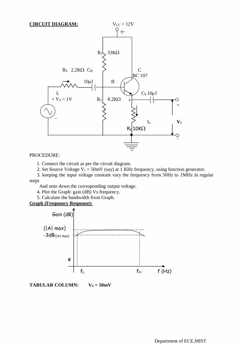
CIRCUIT DIAGRAM: VCC = 12V
R1 33K
RS 2.2K CB C
BC 107
10f B
E
Ii CE 10f
+ VS = 1V R2 8.2K E
+
+
_
Io V0
RE 10K
–
PROCEDURE:
1. Connect the circuit as per the circuit diagram.
2. Set Source Voltage Vs = 50mV (say) at 1 KHz frequency, using function generator.
3. keeping the input voltage constant vary the frequency from 50Hz to 1MHz in regular
steps
And note down the corresponding output voltage.
4. Plot the Graph: gain (dB) Vs frequency.
5. Calculate the bandwidth from Graph.
Graph (Frequency Response):
0
TABULAR COLUMN: VS = 50mV
Gain (dB)
(|A| max)
-3dB(|A| max)
fL fH f (Hz)

Department of ECE,MIST
In the usual application, mid band frequency range are defined as those frequencies at which
the response has fallen to 3dB below the maximum gain (|A| max). These are shown as fL and
fH, and are called as the 3dB frequencies are simply the lower and higher cut off frequencies
respectively. The difference between higher cut-off frequency and lower cut-off frequency is
referred to as bandwidth (fH – fL).
RESULT:
Maximum Gain=
3db Gain= Maximum Gain -3db
Band Width =
Viva Voce Questions
1. Why CC amplifier is known as emitter follower?
2. Mention the applications of CC amplifier. Justify?
3. What is the phase difference between input and output signals in the case of CC
amplifier?
4. Mention the characteristics of CC amplifier?
5. What is gain bandwidth product?
Frequency VO (volts) Gain = Vo/Vs Gain (dB) =20 log10 Vo/Vs)

Department of ECE,MIST
Experiment No: 10
COMMON EMITTER AMPLIFIER
AIM: - To Study the common emitter amplifier and to find
1. Cut off frequencies.
2. Bandwidth.
Components:
EQUIPMENT REQUIRED:
THEORY: The common emitter configuration is widely used as a basic amplifier as
It has both voltage and current amplification.
Resistors R1 & R2 form a voltage divider across the base of the transistor. The function of this
network is to provide necessary bias condition and, ensure that emitter - base junction is
operating in the proper region.
In order to operate transistor as an amplifier, the biasing is done in such a way that the
operating point should be in the active region. For an amplifier the Q-point is placed so that
the load line is bisected. Therefore, in practical design the VCE is always set to VCC/2. This
will conform that the Q-point always swings within the active region. This limitation can be
explained by maximum signal handling capacity. Output is produced without any clipping or
distortion for the maximum input signal. If not so, reduce the input signal magnitude.
The Bypass Capacitor The emitter resistor RE is required to obtain the DC quiescent
stability. However the inclusion of RE in the circuit causes a decrease in amplification at
higher frequencies. In order to avoid such a condition, it is bypassed by capacitor so that it
acts as a short circuit for AC and contributes stability for DC quiescent condition. Hence
capacitor is connected in parallel with emitter resistance.
XCE << RE
E
E
RfC
2
1
Name Qty
Transistor BC 107
Resistors 10K(2),33K,1K
Capacitors 10µf
4.7 µf (1)
1
1
2
Name Qty
Bread Board
CRO
Function generator
Connecting wires
1
1
1

Department of ECE,MIST
E
EfR
C2
1
The Coupling Capacitor An amplifier amplifies the given AC signal. In order to have
noiseless transmission of signal (with out DC), it is necessary to block DC i.e. the direct
current should not enter the amplifier or load. This is usually accomplished by inserting a
coupling capacitor between any two stages.
XCC << (Ri hie)
hie) (Ri2
1
CfC
hie) (Ri2
1
C
CfC
C
Frequency Response Emitter bypass capacitors are used to short circuit the emitter resistor
and thus increase the gain at high frequency. The coupling and bypass capacitors cause the
fall of in the low frequency response of the amplifier because their impedance becomes large
at low frequencies. The stray capacitors are effectively open circuits.
In the mid frequency range the large capacitors are effective short circuits and the stray
capacitors are open circuits, so that no capacitance appears in the mid frequency range.
Hence, the mid band gain is maximum.
At the high frequencies, the bypass and coupling capacitors are replaced by short circuits and
stray capacitors and the transistor determine the response.
CIRCUIT DIAGRAM:
VCC = 12V
RC 4.7K
R1 33K
CC 10f
RS 10K CB C
BC 107
10f B +
Ii B E
+ + VS = 50mV R2 10K RE 1K VO
CE 4.7f
-
-
PROCEDURE:
1. Connect the circuit as per the circuit diagram.
2. Set Source Voltage Vs = 50mV (say) at 1 KHz frequency, using function generator.
3. Keeping the input voltage constant vary the frequency from 50Hz to 1MHz in regular
steps and note down the corresponding output voltage.

Department of ECE,MIST
4. Plot the Graph: gain (dB) Vs frequency.
5. Calculate the bandwidth from Graph.
6. Calculate all the parameters at mid band frequencies (i.e. at 1 KHz).
Graph (Frequency Response):
TABULAR COLUMN:
VS = 50mV
In the usual application, mid band frequency range are defined as those frequencies at which
the response has fallen to 3dB below the maximum gain (|A| max). These are shown as fL and
fH, and are called as the 3dB frequencies are simply the lower and higher cut off frequencies
respectively. The difference between higher cut-off frequency and lower cut-off frequency is
referred to as bandwidth (fH – fL).
RESULT
Maximum Gain=
3db Gain= Maximum Gain -3db
Band Width =
Reasoning Questions
1. How do we test the transistor for active region condition?
2. What are the factors, which influence the higher cut-off frequency?
3. What are the components, which influence the lower cut-off frequency?
Frequency VO (volts) Gain = Vo/Vs Gain (dB) =20 log (V o/Vs)

Department of ECE,MIST
4. Mention the applications of CE amplifier. Justify?
5. Compare the characteristics of CE amplifier, CB amplifier & CC amplifier.
6. What must be the voltage across the transistor, when it is operated as a switch?
7. How do we test the transistor for switching condition?

Department of ECE,MIST
Experiment No: 11
COMMON SOURCE FET AMPLIFIER
AIM: - To Study the JFET Common Source amplifier and to find
1 .Bandwidth
2. Cut off frequencies.
EQUIPMENT REQUIRED:
THEORY:
The possible three configurations of JFET amplifiers, common source (CS)
Configuration is mostly used. The advantage of using CS configuration is that
it has very high input impedance. Figure (1) shows the FET amplifier of
common source configuration. The biasing input and couplings are shown in
the figure. The midrange voltage gain of the amplifier is given by
A=gm (rd || RL)
At the mid-frequency range, there is no effect of input and output coupling
capacitors. Therefore, the voltage gain and phase angle are constant in this
frequency range. The amplifier shown in figure (1) has only two RC networks
that influence its low-frequency response. One network is formed by the
output coupling capacitors and the output impedance looking in at the drain.
Just as in the case of BJT amplifier, the reactance of the input coupling
capacitor, reactance increases as the frequency decreases. The phase angle
also changes with change in frequency.
As the frequency is increased beyond mid-frequency range the internal
transistor capacitance effect is predominant. For JFETs Cgs is the internal
capacitance between gate and source. This is also called input capacitance,
Ciss. The other internal capacitance, which effects the performance is Cgd acts
as a feed back circuit, which couples both, input and output. The effect of both
these capacitances is that it reduced the gain appreciably as in the case of BJT.
Equipment Range Quantity
Common Source JFET amplifier Kit
CRO
Function generator
Connecting wires
(0-20) MHz
(0-1) MHz
1
1
1

Department of ECE,MIST
CIRCUIT DIAGRAM: VDD = 12V
RL
5.6K
C2 10f
C1 10f G D
B
BFW 11
+ S VO
1M CS
VS = 50mV R1 RS 10f
2.2K
-
Figure (1)
PROCEDURE:
1. Connect the circuit as per the circuit diagram.
2. Set Source Voltage Vs = 50mV (say) at 1 KHz frequency, using function generator.
3. keeping the input voltage constant vary the frequency from 50Hz to 1MHz in regular steps
and note down the corresponding output voltage.
4. Plot the Graph: gain (dB) Vs frequency.
5. Calculate the bandwidth from Graph.
6. Calculate all the parameters at mid band frequencies (i.e. at 1 KHz).
7. To calculate Voltage Gain:
)(V Voltage Source
)(V VoltageOutput )(AGain Voltage
S
o
VS

Department of ECE,MIST
Graph (Frequency Response
TABULAR COLUMN: VS = 50mV
In the usual application, mid band frequency range are defined as those frequencies at which
the response has fallen to 3dB below the maximum gain (|A| max). These are shown as fL and
fH, and are called as the 3dB frequencies are simply the lower and higher cut off frequencies
respectively. The difference between higher cut-off frequency and lower cut-off frequency is
referred to as bandwidth
(fH – fL)
RESULT:
Maximum Gain=
3db Gain= Maximum Gain -3db
Band Width =
Frequency VO (volts) Gain = Vo/Vs Gain (dB) =20 log (Vo/Vs)
Gain (dB)
(|A| max)
-3dB(|A| max)
fL fH frequency

Department of ECE,MIST
Reasoning Questions
1. What are the advantages of FET amplifier over conventional transistor amplifiers?
2. Voltage gain of a FET is less than a BJT, Why?
3. FET is used as a buffer amplifier, why?
4. Input impedance of MOSFET is much higher than a FET, Why?
5. A MOSFET can be operated with positive or negative gate voltage, why?

Department of ECE,MIST
Experiment No: 12
SCR CHARACTERISTICS
OBJECTIVE: To plot Volt-Ampere Characteristics of SCR.
EQUIPMENT:
Name Range Qty
Bread Board
SCR
Regulated Power Supply
Digital Ammeter
Digital Voltmeter
Connecting Wires
-
0-30V DC
0-200A/200mA
0-20V DC
1
1
2
1
1
THEORY:
SCR is a four layer three junction PNPN silicon semiconductor switching device. It
has a 3 terminals anode, cathode and gate. SCR stands for Silicon Controlled Rectifier. It
acts as a switch when forward biased. When the gate is kept open i.e., gate current IG=0,
operation of SCR is similar to PNPN diode. When IG is less than zero, the amount of reverse
bias applied to J2 is increased. So the break over voltage VBO is increased. When IG is greater
than zero, the amount of reverse bias applied to J2 is decreased thereby decreasing the break
over voltage with very large positive gate current break over may occur at a very low voltage
such that the characteristics if SCR is similar to that of a PN diode. As the voltage at which
the SCR is switched ‘ON’ can be controlled by varying the gate current IG, it is commonly
called as controlled switch. Once SCR is ON, the gate loses control, i.e. the gate cannot be
used to switch the device OFF. One way to turn the device OFF is by lowering the anode
current below the holding current VH, keeping the gate open.
SCR is used in relay control, motor control, phase control, heater control, battery
chargers, inverters, regulated power supplies and as static switches.

Department of ECE,MIST
PROCEDURE:
1. Make connections as shown in circuit diagram.
2. By increasing VGG set the gate current to IG say (40 µA), go on increasing the plate
Supply voltage VBB and read this voltage VAK across anode and cathode .When this
Voltage is equal to the firing voltage (If) of SCR, the voltmeter suddenly deflects back
To low value (say<1) and the SCR fires and anode current suddenly jumps and is read
By multimeter IA . Note down the reading of the volt-meter when it deflects back and at
This point the anode current is approximately equal to zero.
3. After deflection of voltmeter to approximately 1V note down this voltage and
Corresponding anode current. Now further increase the anode supply voltage VBB and
Note down the corresponding anode current IA and anode to cathode voltage VAK.
Repeat this process until VBB =30V and tabulate the result.
4. Repeat the above procedure for different gate currents IG and tabulate the readings.
5. Now plot the V-I characteristics in a graph by taking VAK along x-axis and IA along y-
Axis.

Department of ECE,MIST
OBSERVATIONS:
EXPECTED GRAPH:
IA
(mA)
↑
0 VBO → VAK (Volts)
PRECAUTIONS:
1. While doing the experiment do not exceed the ratings of the SCR. This may lead to
damage the diode.
2. Connect voltmeter and Ammeter in correct polarities as shown in the circuit diagram.
3. Do not switch ON the power supply unless you have checked the circuit connections
as per the circuit diagram.
RESULT: The V-I characteristics of the SCR was plotted.
IG = 40µA IG = 50 µA IG =60 µA
VAK
(Volts)
IA
(mA)
VAK
(Volts)
IA
(mA)
VAK
(Volts)
IA
(mA)

Department of ECE,MIST
VIVA-VOCE QUESTIONS
1. What are the applications of SCR?
2. How can a SCR be turned OFF?
3. Explain the negative resistance characteristic of SCR?

Department of ECE,MIST
Experiment No: 13
UJT CHARACTERISTICS
Objective: To study and plot the emitter characteristics (VE vs IE) of a UJT.
Components:
Name Qty
UJT 2N 2646 1No
Resistors 1K 2No
Equipment:
Name Range Qty
Bread Board
UJT
Regulated Power
Supply
Digital Ammeter
Digital Voltmeter
Connecting Wires
-
0-30V DC
0-20mA
0-20V/30V DC
1
1
2
1
1
Specifications:
For UJT 2N – 2646:
Peak Emitter Current (IP) = 2A
Continuous Emitter Current (IE) = 50mA
Inter Base Voltage (VBB) = 35V
Emitter Base Reverse Voltage (VEB2) = –30V
Power Dissipation at 250C = 300mW
Circuit Diagram:
RBB
2N2646
RE IE (0-20mA) B2 1K
E
(0-30) v 1K
B1
VEE VE VBBI
(0-20V) VBB
(0-20V) (0-30v)

Department of ECE,MIST
Pin assignment of UJT:
Emitter Base -1
Base - 2
Theory: The Uni-junction transistor is a 3-terminal solid-state device (emitter and the
Two bases). Fig (a) shows the symbol of UJT. A simplified equivalent circuit
Is shown in fig (b).
B2
RB2
E VBB
E B2
VE
D1 RB1 VRB1
B1
B1
Fig (a): Symbol of UJT Fig (b): Equivalent Circuit
This device has only one pn junction and hence it is known as
Uni-junction transistor. The PN emitter to base junction is shown as diode D1. The inter base
resistance RBB of the N-type Si bar appears as two resistors RB1 & RB2 where RBB equals the
sum of RB1 & RB2.
Referring to the equivalent circuit
I. When no voltage is applied between B1 and B2 with emitter open, the inter base
resistance is given by RBB = RB1 + RB2.
II. When a voltage VBB is applied between B1 and B2 with emitter open, voltage will
divide up across RB1 & RB2.
BB
B2B1
B1
RB1 VRR
R V
,
B2B1
B1
BB
RB1
RR
R
V
V
VRB1 = VBB where = the intrinsic stand-off ratio B2B1
B1
RR
R
The VBB across RB1 reverse biased diode thereby dropping the emitter current to
zero.
III. When supply is connected at the emitter, the diode is forward biased making the input
voltage to exceed by VD
VP = VBB + VD

Department of ECE,MIST
The emitter conductivity characteristics are such that as IE increases the emitter to base (B1)
voltage decreases. At a peak point Vp and the valley point Vv, the slope of the emitter
characteristics is 0. At points to the left of VB the E-B1 is forward biased and IE exists.
Between Vp & Vv increase in IE is accompanied by a reduction in emitter voltage VE. This is
the negative resistance region of UJT. Beyond the valley point Vv an increase in IE is
accompanied by an increase in VE. This region is known as the saturation region.
Procedure:
1. Make the connections as per circuit diagram.
2. Keep output voltage VBBI = 5V by varying VBB.
3. Varying VEE gradually, note down both emitter current IE and emitter voltage (VE).
4. Step Size is not fixed because of non linear curve and vary the X-axis variable (i.e. if
output variation is more, decrease input step size and vice versa).
5. Repeat above procedure (step 3) for VBBI =10V.
Observations:
Expected Graph: Plot the tabulated readings on a graph sheet with IE on X-axis and VE
on Y-axis
Peak point
VE (V) saturation region
Cutoff Region -ve resistance
Region
Valley point
0 Ip IV IE (mA)
Since the diode is conducting, the resistance between emitter and base (B1) reduces
and hence the internal drop from emitter to B1 decreases.
VBB1 = 5V VBB
1 = 10V
IE (mA) VE (V) IE (mA) VE (V)

Department of ECE,MIST
Inference:
1. There is a negative resistant region from peak point to valley point.
2. Increase in VBBI increases the value of peak and valley voltages.
Precautions:
1. While doing the experiment do not exceed the ratings of the
UJT. This may lead to damage the UJT.
2. Connect voltmeter and Ammeter in correct polarities as shown in the
Circuit diagram.
3. Do not switch ON the power supply unless you have checked the
Circuit connections as per the circuit diagram.
4. Make sure while selecting the emitter, base -1 and base – 2 terminals
Of the UJT.
Result: The emitter characteristics of UJT have been determined.
Viva-voce Questions
1. Specifications of UJT?
2. What is the importance of UJT?
3. When will be UJT is switched?
4. Why UJT is called as a relaxation oscillator?
5. What is a Relaxation Oscillator?

Department of ECE,MIST
ADDITIONAL EPERIMENTS
Experiment No: 1
MEASUREMENT OF h-PARAMETERS OF A TRANSISTOR
AIM: To calculate the hybrid parameters of transistor in CE, CC, CB configurations.
Equipment Required:
Semiconductor trainer module containing:-
Bread board
0-15V power supplies – 2 No’s.
AC power 12-0-12V
Digital voltmeter 0-20V DC
Digital ammeter 0-20µA/mA DC
Components Required:
Transistor BC 107
Resistors 1KΩ – 2 No’s.
Rating of the BC 107 transistor
IC (max) = 200mA
Vceo = 45 V
Ptot = 300mW
Tj = 175d.c.
NPN transistor
Theory:
The terminals behavior of a two port large scale network is specified by two voltages
and two currents. We may select two of the four quantities as independent variables and
express the remaining two in terms of the chosen independent variables. The typical
representation of a two port network is shown in Fig. 801.
If the current i1 and voltage v2 are the independent parameters and if the two ports are
linear, we may write.
V1=h11i1 + h12v2
I2=h21i1 + h22v2

Department of ECE,MIST
The quantities h11’’h12’h21 and h22 are called h-or hybrid parameters because all are not
alike dimensionally but are hybrid in nature i.e., combinations of admittance, impedance and
dimensionless quantities.
The basic assumption in deriving h-mode for a transistor is that the variations about
the quiescent point are small so that the transistor parameters can be considered constant over
the signal excursion. In order to derive transistor hybrid model, we consider the CE circuit.
The voltages and currents related to input and output ports of a transistor respectively in CE
configuration are vb’ib and vc’ic. Hence the h-parameter equations related to transistor can be
written as:
Vb=hieib + hrevc
IC=hfeib + hoevc
Where
hie = ∂vb/∂ib | vc, hre = ∂vb/∂vc | vib ,
hfe = ∂iC/∂iIb | vc, and hoe = ∂ic/∂vc | ih ,
Calculation of h-parameters from the family of input and output parameters for CE
configuration is explained below.
hfe: From the definition hfe is the short circuited forward current grain and is a
dimensionless parameter. This parameter can be calculated from the graph as follows.
hfe = ∂ic/∂iB ≈ ∆ic/∆iB | vc = ic2-ic1 / iB2 – iB1
The current increments are taken around Q point, which corresponds to base current IB=iB
and VCE=Vc.
Hfe = β’ = small signal current gain and
Β = hfe = large signal current gain.
hoe: It gives the output admittance with input open circuited and the units are ohms. This
parameter can be calculated from the graph using the formula given below.
12
12|cc
cciB
c
c
c
coe
vv
ii
v
i
v
ih
The above two h-parameters can be calculated from the family of output characteristics of the
given configuration. We can calculate other two h-parameters from the family of input
characteristics as explained below.

Department of ECE,MIST
hre: It is defined as open circuited reverse voltage gain and is a dimensionless quantity. This
parameter can be calculated from the graph using the formula given below.
12
12|cc
BBIB
c
B
c
Bre
vv
iv
v
v
v
vh
hie: By definition hie represents input impedance when output terminals are short circuited
and its units are ohms. It can be calculated suing formula given below.
12
12|BB
BBvc
B
B
B
Boe
ii
vv
i
v
i
vh
Circuit Diagram:
Procedure:
1. Connect a common emitter transistor configuration circuit for plotting its input
characteristics as shown in fig.8.3.
2. Take a family of readings for variation in IB with VEB at different fixed values of
output voltage VCE.
3. Tabulate the readings and plot the input characteristic curves of CE configuration.
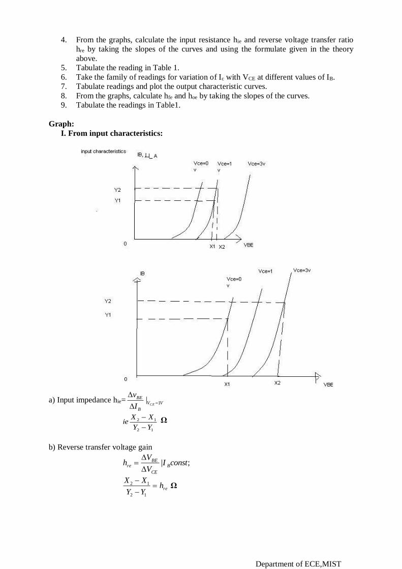
Department of ECE,MIST
4. From the graphs, calculate the input resistance hie and reverse voltage transfer ratio
hre by taking the slopes of the curves and using the formulate given in the theory
above.
5. Tabulate the reading in Table 1.
6. Take the family of readings for variation of Ic with VCE at different values of IB.
7. Tabulate readings and plot the output characteristic curves.
8. From the graphs, calculate hfe and hoe by taking the slopes of the curves.
9. Tabulate the readings in Table1.
Graph:
I. From input characteristics:
a) Input impedance hie= VV
B
BE
CEI
v1|
12
12
YY
XXie
Ω
b) Reverse transfer voltage gain
;| constIV
Vh B
CE
BEre
rehYY
XX
12
12 Ω

Department of ECE,MIST
II. From output characteristics:
(a)
Forward transfer current ratio:
i.e. 12
12
XX
YYh fe
Output conductance
;| constII
Ih B
CE
Coc
.12
12 VXX
YYhoe
;| constVI
Ih CE
B
Cre

Department of ECE,MIST
Sino. h parameters Value
1
2
3
4
Current gain, hfe
Output Admittance, hoe
Reverse voltage gain, hre
Input impedance, hie
Table – 1.
Result:
The h parameters for a transistor in CE configuration are calculated.
1. Input Impedance hie = ohms
2. Reverse transfer voltage gain hre =
3. Forward transfer current ratio hfe =
4. Output conductance hoe = mhos.
Viva-Voce Questions
1. What is the range of values of Input Impedance hie in CB CE, CC and why?
2. What is the range of values of Reverse transfer voltage gain her in CB, CE, CC and why
3. What is the range of values of Forward transfer current ratio hfe in CB,CE,CC and why
4. What is the range of values of Output conductance hoe in CB CE, CC and why?

Department of ECE,MIST
BRIDGE RECTIFIERS
AIM: To Rectify the AC signal and then to find out Ripple factor and percentage of
Regulation in Full-wave Bridge rectifier circuit with and without Capacitor filter.
APPARATUS:
S.No Name Range / Value
1 Transformer 230V / 0-9V
2 Diode 1N4001
3 Capacitors 1000F/16V, 470f/25V
4 Decade Resistance Box -
5 Multimeter -
6 Bread Board and connecting wires -
7 Dual Trace CRO 20MHz
PROCEDURE:
WITHOUT FILTER:
1. Connecting the circuit on bread board as per the circuit diagram. 2. Connect the primary of the transformer to main supply i.e. 230V, 50Hz
3. Connect the decade resistance box and set the RL value to 100Ω 4. Connect the Multimeter at output terminals and vary the load resistance (DRB)
from 100Ω to 1KΩ and note down the Vac and Vdc as per given tabular form
5. Disconnect load resistance ( DRB) and note down no load voltage Vdc (V no load) 6. Connect load resistance at 1KΩ and connect Channel – II of CRO at output
terminals and CH – I of CRO at Secondary Input terminals observe and note down the Input and Output Wave form on Graph Sheet.
7. Calculate ripple factor V
ac
Vdc
8. Calculate Percentage of Regulation, % Vno load
Vfull load 100% V
no load WITH CAPACITOR FILTER:
1. Connecting the circuit as per the circuit Diagram and repeat the above
procedure from steps 2 to 8.

Department of ECE,MIST
Tabular Column:
Vac = _____ (Voltage across the secondary of the transformer)
Condition Vac Vdc Vm R
Without Filter
Condition Vac Vdc Vm C R
With C Filter
RESULT: Observe Input and Output Wave forms and Calculate ripple factor and
percentage of regulation in Full-wave Bridge rectifier with and without filter.
Without Filter:
Ripple Factor : Regulation :
With Capacitor Filter: Ripple Factor : Regulation :
PRECAUTIONS: 1. Check the wires for continuity before use. 2. Keep the power supply at Zero volts before Start. 3. All the contacts must be intact.
VIVA QUESTIONS: 1. What are the advantages of Bridge Rectifier over the center tapped Rectifier? 2. What does Regulation indicate?

EDC LABORATORY MANUAL
Department of ECE,MIST