
P Low Power Current Mode Oscillator based Quantizer ... · Oscillator based Quantizer. Thesis by...
71
Low Power Current Mode Δ ∑ ADC using a Ring Oscillator based Quantizer. Thesis by Ibrahim Kazi School of Information and Communication Technology Royal Institute of Technology, Sweden In Partial Fulfillment of the Requirements For the Degree of Master of Science in System on Chip Design Supervisor Nikola Katic, LSM, EPFL Prof.Alexandre Schmid, LSM, EPFL Stockholm, Sweden August, 2012
-
Upload
truongkhuong -
Category
Documents
-
view
227 -
download
2
Transcript of P Low Power Current Mode Oscillator based Quantizer ... · Oscillator based Quantizer. Thesis by...
Low Power Current Mode ∆∑
ADC using a Ring
Oscillator based Quantizer.
Thesis by
Ibrahim Kazi
School of Information and Communication Technology
Royal Institute of Technology, Sweden
In Partial Fulfillment of the Requirements
For the Degree of
Master of Science in System on Chip Design
Supervisor Nikola Katic, LSM, EPFL
Prof.Alexandre Schmid, LSM, EPFL
Stockholm, Sweden
August, 2012
ACKNOWLEDGEMENTS
I would like to thank Dr.Alexandre Schmid and Nikola Katic for providing me the
opportunity for this thesis at the Microelectronics Systems Lab, EPFL. Nikola helped
me a lot in the design phase and simulations during this thesis, for this I am greatly
indebted to him. I would like to thank Prof.Dr.Ana Rusu from the RAMSIS group
KTH for not only agreeing to be my thesis examiner, but also equipping me with
the necessary knowledge about data converters to undertake a masters thesis in this
field. Particulary her advanced mixed mode design course which helped me a long
way in this thesis. I would like to thank Dr.Saul Rodriguez Duenas for teaching us
the qualitative way of analyzing analog circuits. The atmosphere here at LSM lab
has been very conducive towards research, for this I thank the LSM group members.
I am forever thankful to my family who have supported me in every way possible and
for being there for me.
2

ABSTRACT
Low power ADCs have wide application from battery operated systems like biomed-
ical devices to on chip power measurement. A more digital implementation is also
desirable to keep up with the technology scaling in digital CMOS design. This thesis
explores the idea of a low power Continuous Time ∆∑
ADC using current mode sig-
naling. It achieves a second order noise shaping by using a first order current filter,
digital difference block and a current controlled ring oscillator. This type of ADC has
a mostly digital implementation, as the main analog block are the current filter and
two op-amps which are used for biasing.
The ADC model is simulated in VerilogA and at the transistor level using UMC
180nm library in CADENCE. MonteCarlo simulation are also performed to ensure
the proper operation of the current filter in presence of mismatches, as log-domain
filters are very sensitive to transistors mismatches.
The ADC specifications obtained at the transistor level simulation are 7.3 Effecitve
Number of Bits (ENOB) over 30KHz bandwidth and 5.3µW power consumption.
3
TABLE OF CONTENTS
List of Figures 7
List of Abbrevations 10
1 Introduction 12
1.1 Motivation . . . . . . . . . . . . . . . . . . . . . . . . . . . . . . . . . 12
1.2 Thesis Organization . . . . . . . . . . . . . . . . . . . . . . . . . . . . 13
1.3 Background on Sigma Delta Modulation . . . . . . . . . . . . . . . . 13
2 Oscillator Based Quantizer 16
2.1 First Order Noise Shaping . . . . . . . . . . . . . . . . . . . . . . . . 16
2.2 Ring Oscillator Quantizer (ROQ) and Edge Detection Circuit . . . . 17
2.3 Dynamic Element Matching . . . . . . . . . . . . . . . . . . . . . . . 19
2.4 Closed-Loop Operation . . . . . . . . . . . . . . . . . . . . . . . . . . 20
3 System Implementation and Verification 22
3.1 Behavioral Model . . . . . . . . . . . . . . . . . . . . . . . . . . . . . 22
3.2 Ring Oscillator Quantizer . . . . . . . . . . . . . . . . . . . . . . . . 27
3.2.1 Inverter Cell for ROQ . . . . . . . . . . . . . . . . . . . . . . 27
3.2.2 Sustained Oscillations . . . . . . . . . . . . . . . . . . . . . . 30
3.2.3 Inverter Cell with Replica Bias and Input Current Mirror . . . 32
4
5
3.2.4 13 stage Ring Oscillator . . . . . . . . . . . . . . . . . . . . . 33
3.2.5 Simulation of ∆∑
ADC using Transistor based Ring Oscillator 34
3.3 Current Filter . . . . . . . . . . . . . . . . . . . . . . . . . . . . . . . 34
3.3.1 Current Conveyor based Current Integrator-I . . . . . . . . . . 35
3.3.2 Current Integrator-II . . . . . . . . . . . . . . . . . . . . . . . 38
3.3.3 Companding Current Integrator-III . . . . . . . . . . . . . . . 39
3.3.4 Simulation Result . . . . . . . . . . . . . . . . . . . . . . . . . 43
3.4 Digital to Analog Converter . . . . . . . . . . . . . . . . . . . . . . . 44
3.4.1 Data Weighted Averaging . . . . . . . . . . . . . . . . . . . . 46
3.4.2 Digital Circuits . . . . . . . . . . . . . . . . . . . . . . . . . . 47
3.4.3 Simulation Results using Transistor Model for DAC and Digital
Circuits . . . . . . . . . . . . . . . . . . . . . . . . . . . . . . 49
3.5 OTAs for Replica Bias and Gain Boosted Current Mirror . . . . . . . 50
4 Simulation Results - Evolution of SNR/SNDR going from Behav-
ioral Model to Transistor Model 53
4.1 MonteCarlo Simulation for Mismatch . . . . . . . . . . . . . . . . . . 58
4.2 Final ADC Specifications . . . . . . . . . . . . . . . . . . . . . . . . . 58
4.3 Comparison with other state of the art CT-∆∑
ADC . . . . . . . . 59
5 Summary 61
5.1 Conclusion . . . . . . . . . . . . . . . . . . . . . . . . . . . . . . . . . 61
5.2 Future Work . . . . . . . . . . . . . . . . . . . . . . . . . . . . . . . . 61
Appendices 63
A Appendix A Verilog-A Code for Oscillator Model 64

6
References 66

List of Figures
1.1 Spectrum of quantization noise at two different sampling frequencies.
The shaded area shows the inband quantization noise . . . . . . . . . 13
1.2 Spectrum of quantization noise with noise shaping. The shaded area
shows the inband quantization noise . . . . . . . . . . . . . . . . . . 14
1.3 ADC in a feedback loop . . . . . . . . . . . . . . . . . . . . . . . . . 15
1.4 Linear model of an ADC in a feedback loop . . . . . . . . . . . . . . 15
2.1 First order noise shaping in oscillator based Analog to Digital Con-
verter (ADC).[1] . . . . . . . . . . . . . . . . . . . . . . . . . . . . . 17
2.2 Frequency to digital converter . . . . . . . . . . . . . . . . . . . . . . 18
2.3 Ring Oscillator with First Order Difference Logic [1] . . . . . . . . . 19
2.4 Open loop model of a ROQ . . . . . . . . . . . . . . . . . . . . . . . 20
2.5 Model of ROQ in a feedback loop . . . . . . . . . . . . . . . . . . . . 20
3.1 Complete Block Level Diagram . . . . . . . . . . . . . . . . . . . . . 23
3.2 Power Spectral Density of the VerilogA model of the ∆∑
ADC.Input:
-12dBFS, 2.75KHz, Bandwidth: 25KHz, Sampling frequency: 1.024MHz 25
3.3 SNR and SNDR vs Input amplitude . . . . . . . . . . . . . . . . . . . 26
3.4 SNR and SNDR vs Input amplitude for a non-linear frequency tuning
curve . . . . . . . . . . . . . . . . . . . . . . . . . . . . . . . . . . . . 26
7

8
3.5 Even inverter ring with differential inverters . . . . . . . . . . . . . . 27
3.6 Inverter Cell for the Ring Oscillator . . . . . . . . . . . . . . . . . . . 28
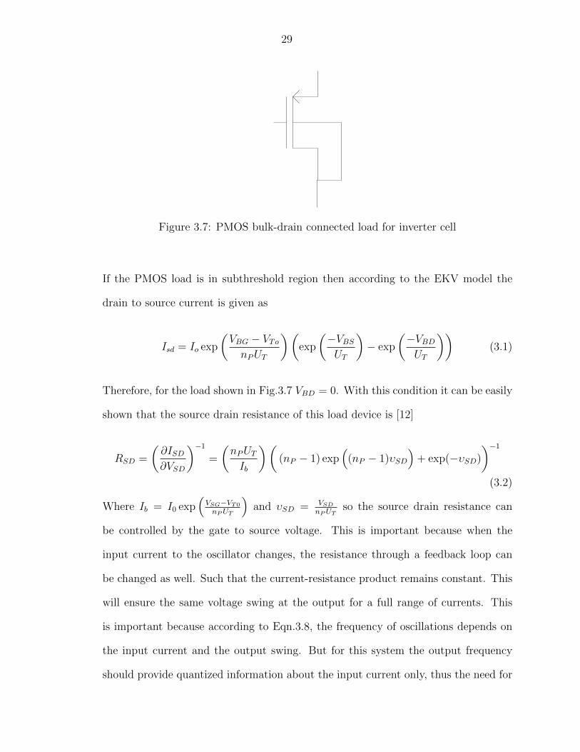
3.7 PMOS bulk-drain connected load for inverter cell . . . . . . . . . . . 29
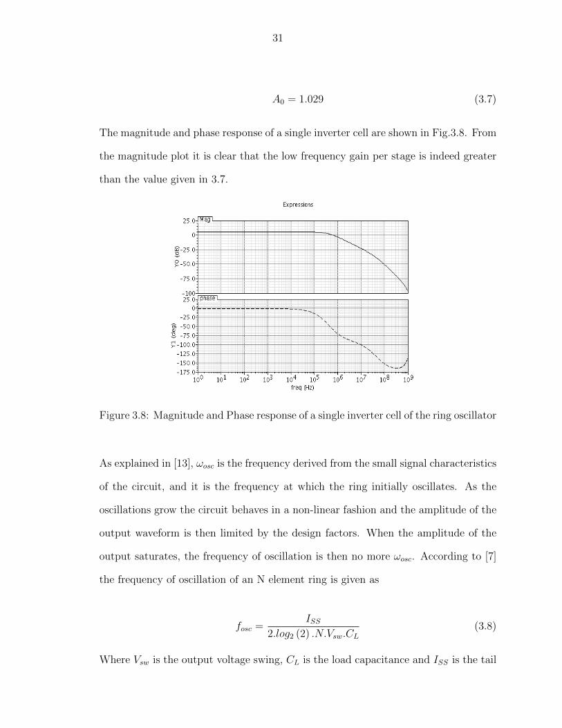
3.8 Magnitude and Phase response of a single inverter cell of the ring
oscillator . . . . . . . . . . . . . . . . . . . . . . . . . . . . . . . . . . 31
3.9 (a)Replica Bias for constant output swing. (b)Inverter with high impedance
current mirror . . . . . . . . . . . . . . . . . . . . . . . . . . . . . . . 33
3.10 Current Controlled Ring Oscillator Linearity and Curve Fitting Show-
ing Third Order Polynomial . . . . . . . . . . . . . . . . . . . . . . . 34
3.11 Power Spectral Density of ∆∑
ADC with transistor based Oscillator
and parasitic load capactance.Input: -12dBFS, 2.75KHz, Bandwidth:
25KHz, Sampling frequency: 1.024MHz . . . . . . . . . . . . . . . . . 35
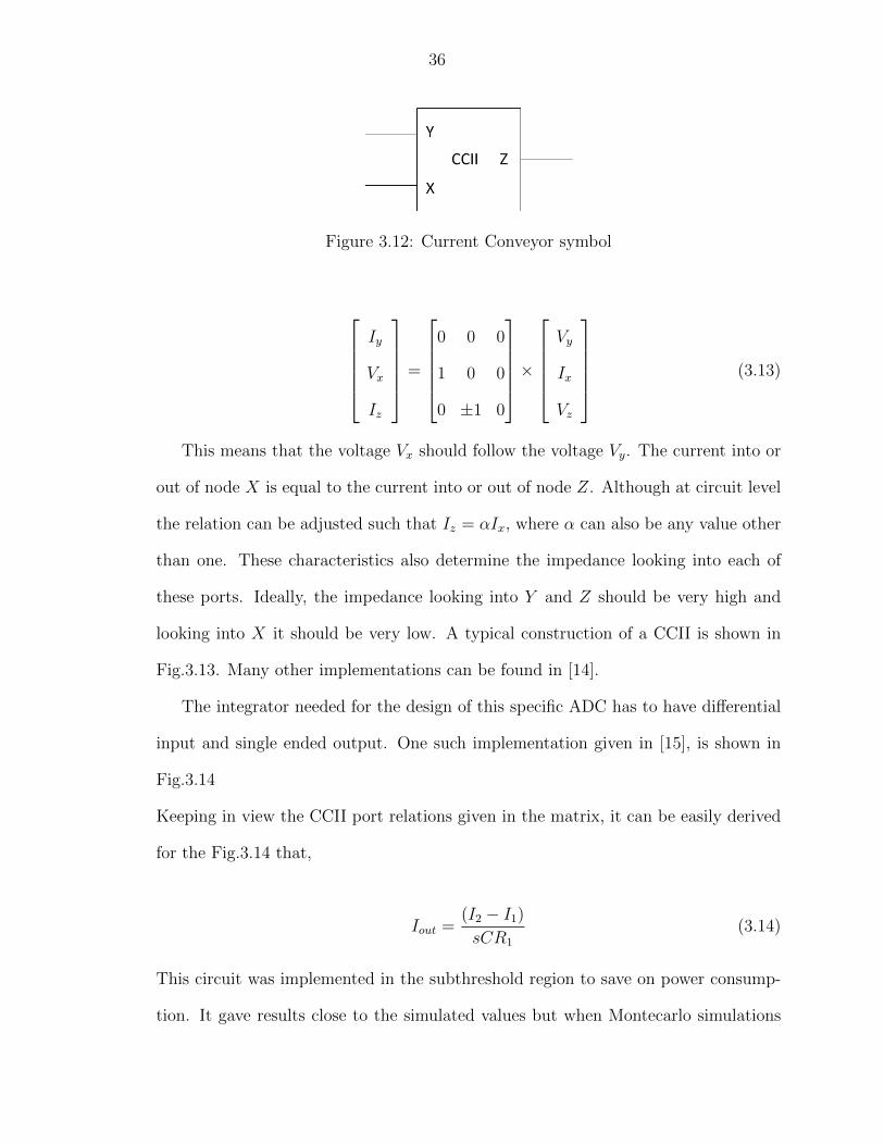
3.12 Current Conveyor symbol . . . . . . . . . . . . . . . . . . . . . . . . 36
3.13 Current Conveyor schematic . . . . . . . . . . . . . . . . . . . . . . . 37
3.14 Current Conveyor based current integrator . . . . . . . . . . . . . . . 38
3.15 Second Integrator: Mismatches between M1 and M4 cause a large bias
current variation if the transistors are in subthreshold . . . . . . . . . 38
3.16 An example of a translinear loop . . . . . . . . . . . . . . . . . . . . 40
3.17 Companding Integrator used in the ∆∑
ADC . . . . . . . . . . . . . 41
3.18 Differential to single ended conversion . . . . . . . . . . . . . . . . . . 43
3.19 SNDR and SNR vs Input Amplitude . . . . . . . . . . . . . . . . . . 44
3.20 Schematic of the feedback DAC . . . . . . . . . . . . . . . . . . . . . 45
3.21 Circuit to create a Negative Replica of the DAC Output Current. (WL
=
0.2413µm for all transistors) . . . . . . . . . . . . . . . . . . . . . . . . . 46
3.22 Each element of the DAC is accessed almost equally over one period
of the test signal. (Test signal -12dBFS, 2.75KHz) . . . . . . . . . . . 47
9
3.23 One of the 13 digital circuits connected at each output of the ring
oscillator . . . . . . . . . . . . . . . . . . . . . . . . . . . . . . . . . . 48
3.24 Schematic of the D flip flop . . . . . . . . . . . . . . . . . . . . . . . 48
3.25 Schematic of the D flip flop . . . . . . . . . . . . . . . . . . . . . . . 49
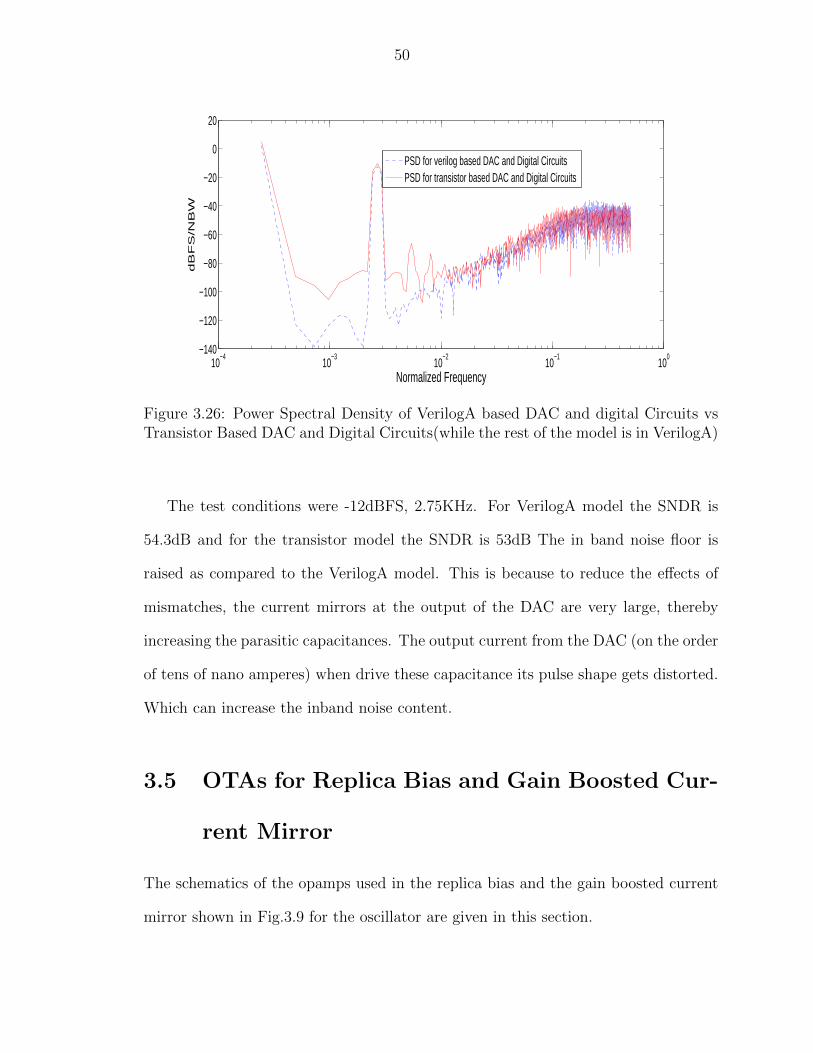
3.26 Power Spectral Density of VerilogA based DAC and digital Circuits vs
Transistor Based DAC and Digital Circuits(while the rest of the model
is in VerilogA) . . . . . . . . . . . . . . . . . . . . . . . . . . . . . . . 50
3.27 Opamp used in the replica bias for constant output swing of the oscillator 51
3.28 Opamp used in the gain boosting of the current mirror input stage of
the oscillator . . . . . . . . . . . . . . . . . . . . . . . . . . . . . . . 52
4.1 SNR and SNDR vs input amplitude-Complete Behavioral Model . . . 54
4.2 SNDR(VerilogA model) vs SNDR(Transistor model for Integrator) . . 54
4.3 SNDR(VerilogA model) vs SNDR(Transistor model for Integrator) vs
SNDR(Transistor model for Integrator and Oscillator) . . . . . . . . . 55
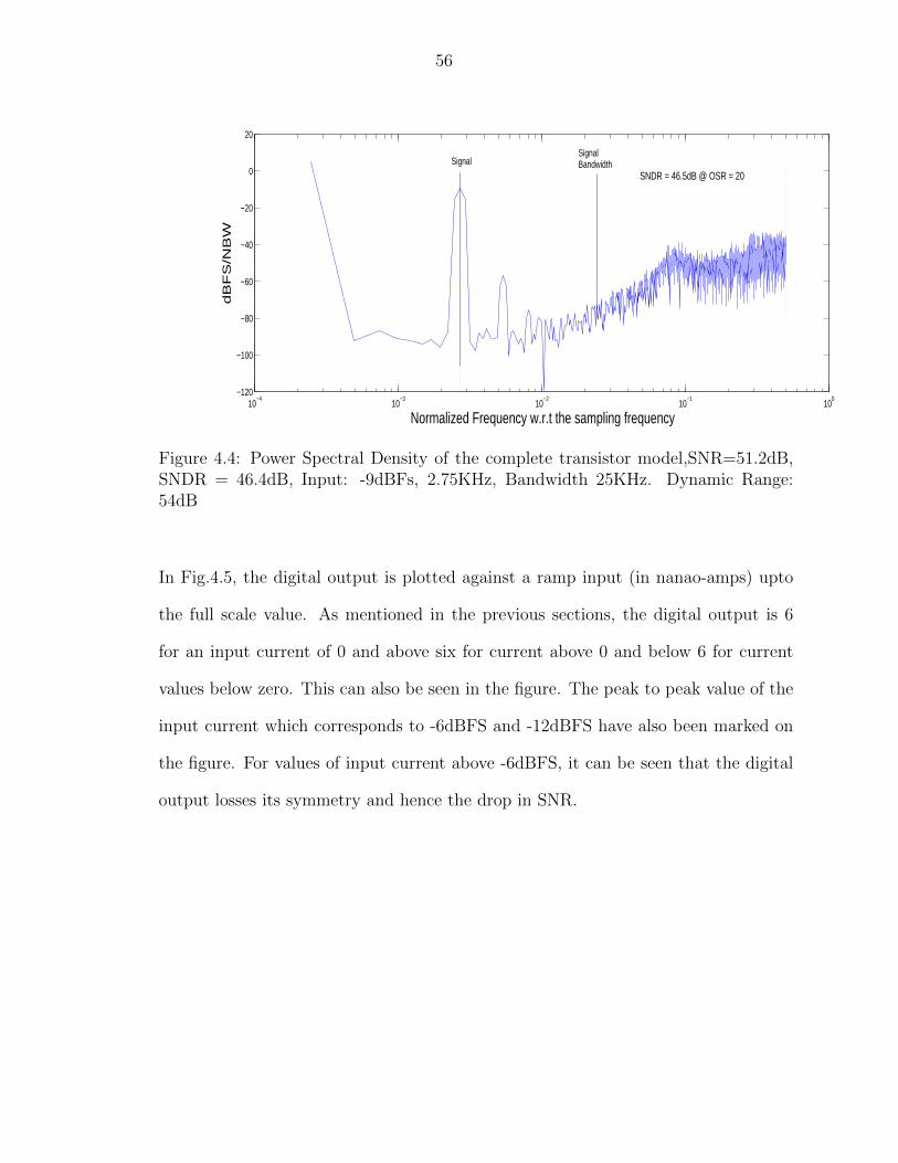
4.4 Power Spectral Density of the complete transistor model,SNR=51.2dB,
SNDR = 46.4dB, Input: -9dBFs, 2.75KHz, Bandwidth 25KHz. Dy-
namic Range: 54dB . . . . . . . . . . . . . . . . . . . . . . . . . . . . 56
4.5 Digital Output vs peek to peek ramp input . . . . . . . . . . . . . . . 57
4.6 Digital Output(filtered) vs peek to peek ramp input . . . . . . . . . . 57
List of Abbrevations
ADC Analog to Digital Converter.
CCII Current Conveyor-Second Generation.
CCO Current Controlled Oscillator.
DAC Digital to Analog Converter.
DEM Dynamic Element Matching.
DWA Dynamic Weighted Averaging.
ENOB Effecitve Number of Bits.
FDC Frequency to Digital Converter.
FOM Figure of Merit.
MCML MOS Current Mode Logic.
NTF Noise Transfer Function.
PLL Phase Locked Loop.
PSD Power Spectral Density.
10
11
ROQ Ring Oscillator Quantizer.
SCL Source Coupled Logic.
SNDR Signal to Noise Distortion Ratio.
SNR Signal to Noise Ratio.
XOR Exclusive OR.
Chapter 1
Introduction
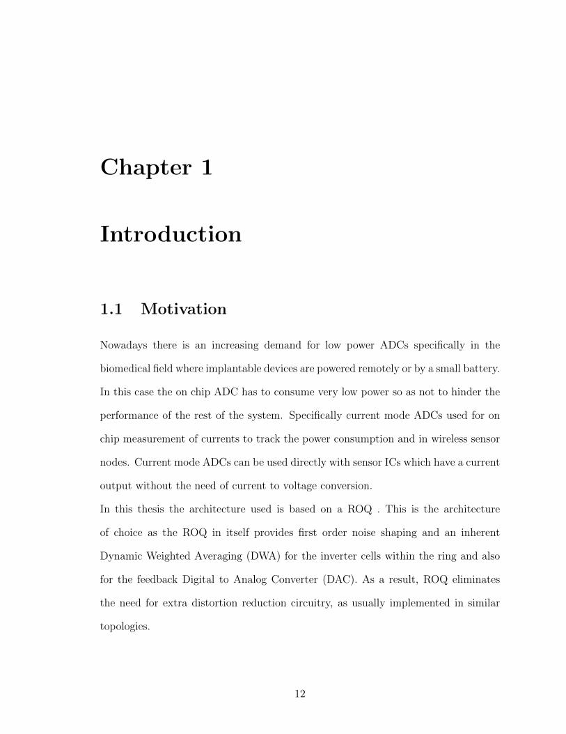
1.1 Motivation
Nowadays there is an increasing demand for low power ADCs specifically in the
biomedical field where implantable devices are powered remotely or by a small battery.
In this case the on chip ADC has to consume very low power so as not to hinder the
performance of the rest of the system. Specifically current mode ADCs used for on
chip measurement of currents to track the power consumption and in wireless sensor
nodes. Current mode ADCs can be used directly with sensor ICs which have a current
output without the need of current to voltage conversion.
In this thesis the architecture used is based on a ROQ . This is the architecture
of choice as the ROQ in itself provides first order noise shaping and an inherent
Dynamic Weighted Averaging (DWA) for the inverter cells within the ring and also
for the feedback Digital to Analog Converter (DAC). As a result, ROQ eliminates
the need for extra distortion reduction circuitry, as usually implemented in similar
topologies.
12
13
1.2 Thesis Organization
A basic background on ∆∑
converters is given in Chapter 1. Signal to Noise Ratio
(SNR) improvement due to oversampling and noise shaping is explained. In Chapter 2
the theory behind a ring oscillator intrinsic noise shaping and data weighted averaging
is given. In chapter 3 behavioral model of the system is simulated and (one by one)
the VerilogA models are replaced with their transistor equivalent and the effect on
SNR and Signal to Noise Distortion Ratio (SNDR) is shown. Finally the complete
transistor based model is simulated and results given. MonteCarlo simulations were
also performed, and the circuit model was adapted to achieve better matching.
1.3 Background on Sigma Delta Modulation
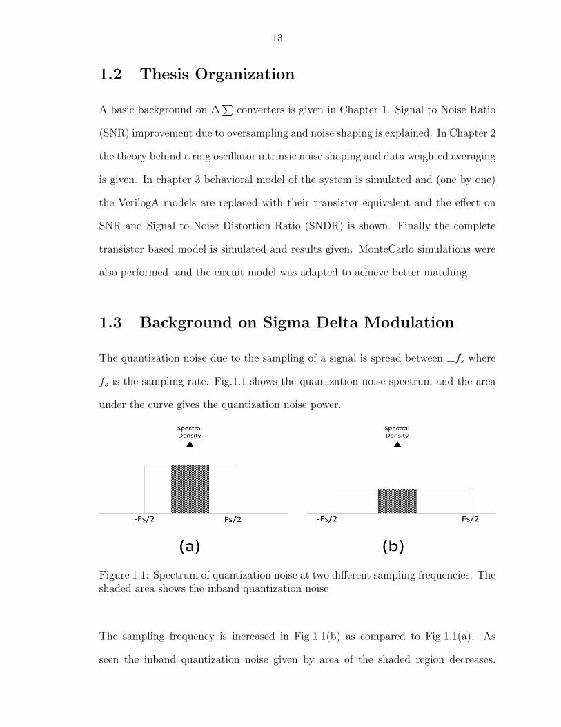
The quantization noise due to the sampling of a signal is spread between ±fs where
fs is the sampling rate. Fig.1.1 shows the quantization noise spectrum and the area
under the curve gives the quantization noise power.
Figure 1.1: Spectrum of quantization noise at two different sampling frequencies. Theshaded area shows the inband quantization noise
The sampling frequency is increased in Fig.1.1(b) as compared to Fig.1.1(a). As
seen the inband quantization noise given by area of the shaded region decreases.
14
But the total quantization noise power in between ±fs remains same for both the
sampling rate. The total quantization noise power depends on the difference between
two adjacent quantization levels and not the sampling frequency [2]. To quantize
the improvement in SNR due to sampling above the Nyquist rate, the over sampling
ratio is defined as OSR = fs2fb
, which shows how many times above the Nyquist rate
is the ADC over sampled. For an N-bit Nyquist rate ADC the SNR is given as
SNR = 6.02N + 1.76. But with over sampling this is now [2]
SNRmax = 6.02N + 1.76 + 10log10 (OSR) (1.1)
This mean there is a 3-dB increase in SNR every time the sampling rate is doubled.
Over sampling alone might not be that power efficient as doubling the sampling
frequency can cause large increase in power consumption. Thus, over sampling is
usually used along with noise shaping techniques in which the quantization noise is
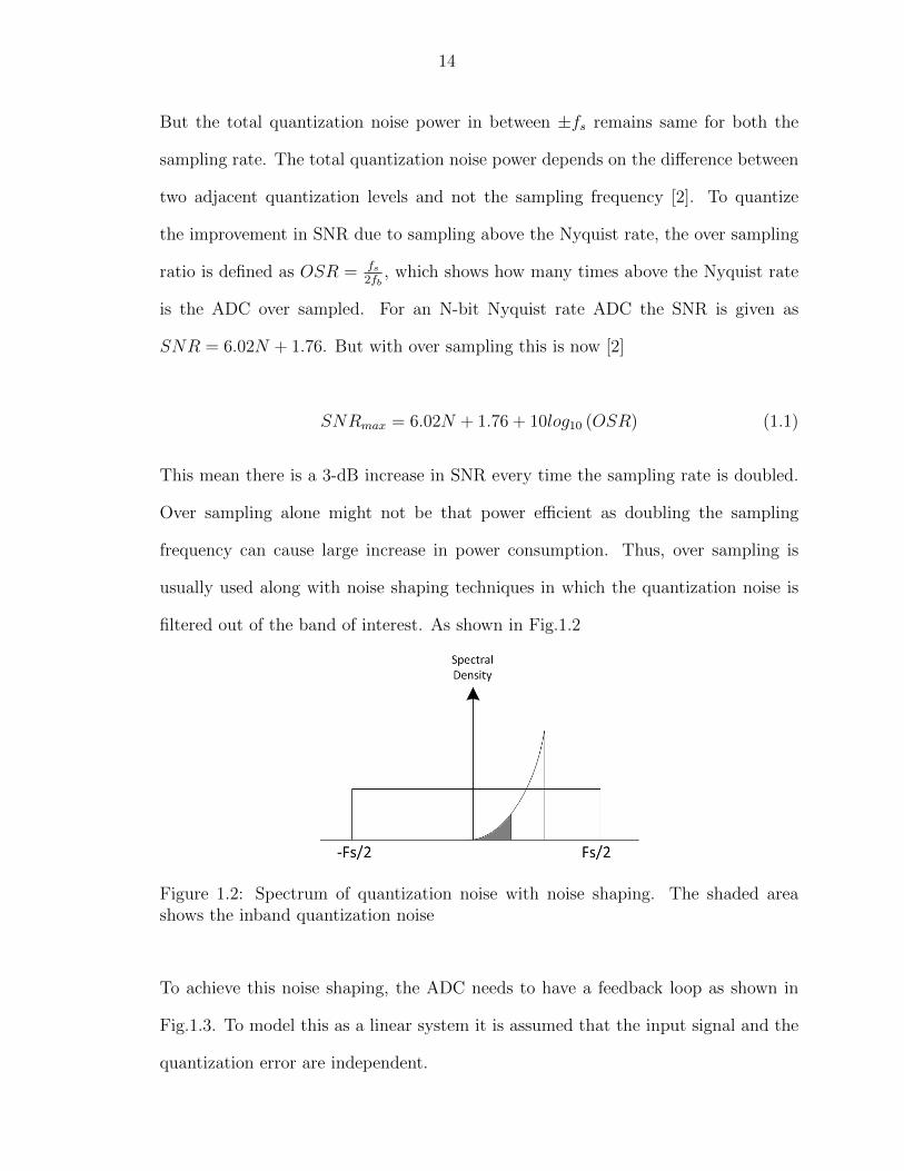
filtered out of the band of interest. As shown in Fig.1.2
Figure 1.2: Spectrum of quantization noise with noise shaping. The shaded areashows the inband quantization noise
To achieve this noise shaping, the ADC needs to have a feedback loop as shown in
Fig.1.3. To model this as a linear system it is assumed that the input signal and the
quantization error are independent.
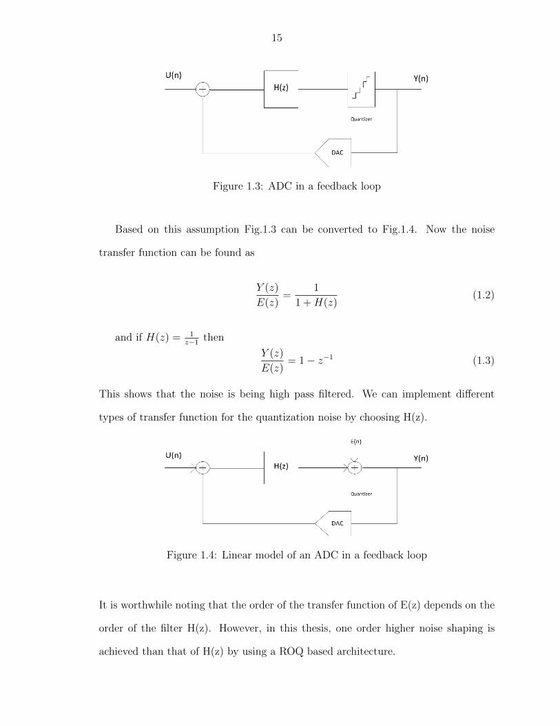
15
Figure 1.3: ADC in a feedback loop
Based on this assumption Fig.1.3 can be converted to Fig.1.4. Now the noise
transfer function can be found as
Y (z)
E(z)=
1
1 +H(z)(1.2)
and if H(z) = 1z−1 then
Y (z)
E(z)= 1 − z−1 (1.3)
This shows that the noise is being high pass filtered. We can implement different
types of transfer function for the quantization noise by choosing H(z).
Figure 1.4: Linear model of an ADC in a feedback loop
It is worthwhile noting that the order of the transfer function of E(z) depends on the
order of the filter H(z). However, in this thesis, one order higher noise shaping is
achieved than that of H(z) by using a ROQ based architecture.
Chapter 2
Oscillator Based Quantizer
As seen in the previous chapter, the order of the loop filter determines the order of the
quantization noise shaping. In this thesis, instead of using conventional comparator
based quantizer, we use a Current Controlled Oscillator (CCO) based quantizer which
increases the order of the noise shaping by one more than the order of the loop filter.
Before the CCO is presented in the closed loop sigma delta topology, a brief intro is
given about the oscillator as a stand alone ADC.
2.1 First Order Noise Shaping
Consider an oscillator whose output is sampled by a counter. The basic concept of
the first order noise shaping in an oscillator is explained in [3][4][5][1] and shown in
Fig.2.1. The counter value is equal to the number of rising edges in the output of the
ring oscillator. This mean that whenever there is a phase shift of 2π the counter is
incremented by one.
The number of rising edges (or the frequency of oscillation) are proportional to
the input voltage or current. There is a truncation error left at the end of each cycle.
Consequently this amount of the signal is missing from the next cycle. Therefore
16

17
Figure 2.1: First order noise shaping in oscillator based ADC.[1]
each cycle has a missing part of the oscillator signal from the previous cycle and a
quantization error of its own cycle. The total quantization error in one period is then
E(n) = q(n) − q(n− 1) (2.1)
E(z) = Q(z)(1 − z−1) (2.2)
The quantization noise is thus high-pass filtered. To use a multi-bit quantizer, a ring
oscillator can be used which provides multiple phases of the output waveform. Using
a counter which has a reset operation can degrade noise shaping as it adds further
latency and can increase the quantization noise if the oscillator edge occurs in close
proximity to the counter reset signal [6].
2.2 ROQ and Edge Detection Circuit
An alternative to the counter implementation is given in [5]. The configuration in
Fig.2.2 provides the first order difference as it detects the transitions in the oscillator
output. The XOR gate compares the current and previous sample of the signal and
detects if there has been a transition. The total number of transitions detected are

18
proportional to the input signal, and give the quantized form of the input signal. The
Figure 2.2: Frequency to digital converter
complete configuration of the ring oscillator and the Frequency to Digital Converter
(FDC) slice can be seen in Fig.2.3. The FDC slices operating in parallel give a multi
bit operation. For the proper operation of the ring oscillator, the total number of
transitions in a clock period should not exceed the total number of stages in the
oscillator, as this will result in incorrect count. This condition can be expressed as
fosc < fs/2 (2.3)
Now for an ADC based on the configuration showed in Fig.2.3 the maximum SNR
that can be achieved is given in [5] as
SNR = 10log10(9f 3
s (2NTsKvAm)2
4π2f 3b
) (2.4)
Where fs is the sampling frequency,Kv is the frequency to voltage (in this case fre-
quency to current) gain. N is the number of delay elements.fb is the signal bandwidth.
Ts is the sampling period and Am is the signal amplitude.
19
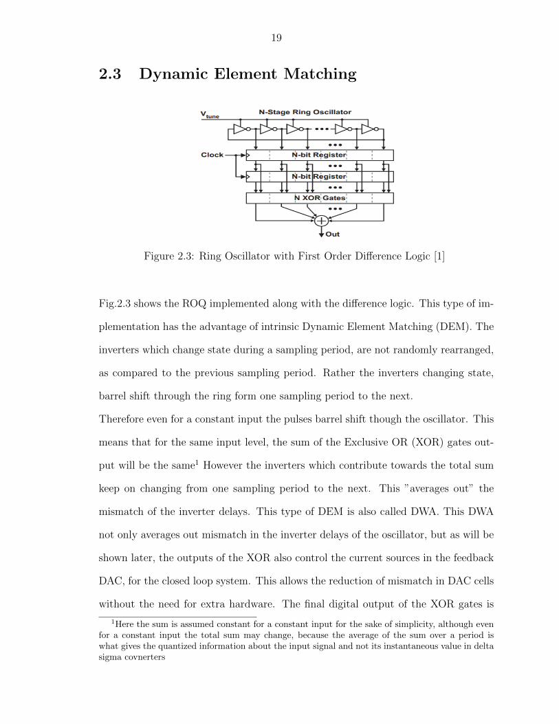
2.3 Dynamic Element Matching
Figure 2.3: Ring Oscillator with First Order Difference Logic [1]
Fig.2.3 shows the ROQ implemented along with the difference logic. This type of im-
plementation has the advantage of intrinsic Dynamic Element Matching (DEM). The
inverters which change state during a sampling period, are not randomly rearranged,
as compared to the previous sampling period. Rather the inverters changing state,
barrel shift through the ring form one sampling period to the next.
Therefore even for a constant input the pulses barrel shift though the oscillator. This
means that for the same input level, the sum of the Exclusive OR (XOR) gates out-
put will be the same1 However the inverters which contribute towards the total sum
keep on changing from one sampling period to the next. This ”averages out” the
mismatch of the inverter delays. This type of DEM is also called DWA. This DWA
not only averages out mismatch in the inverter delays of the oscillator, but as will be
shown later, the outputs of the XOR also control the current sources in the feedback
DAC, for the closed loop system. This allows the reduction of mismatch in DAC cells
without the need for extra hardware. The final digital output of the XOR gates is
1Here the sum is assumed constant for a constant input for the sake of simplicity, although evenfor a constant input the total sum may change, because the average of the sum over a period iswhat gives the quantized information about the input signal and not its instantaneous value in deltasigma covnerters

20
thermometer coded. So the sum of all XOR gates output gives the final digital output
2.4 Closed-Loop Operation
As seen in the previous section, using a ROQ as a stand alone ADC provides first order
noise shaping. Using the ROQ in a ∆∑
feedback loop improves the distortions in
the output caused by the the non-linear tuning curve [1]. This feedback also provides
for a second order noise shaping of the quantization noise.
Figure 2.4: Open loop model of a ROQ
Fig.2.4 shows the open loop model of the ROQ [7]. The difference block is imple-
mented by the frequency to digital converter where the integrator is inherent in the
oscillator. Placing ROQ in a feedback is shown in Fig.2.5
Figure 2.5: Model of ROQ in a feedback loop
21
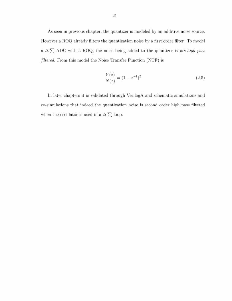
As seen in previous chapter, the quantizer is modeled by an additive noise source.
However a ROQ already filters the quantization noise by a first order filter. To model
a ∆∑
ADC with a ROQ, the noise being added to the quantizer is pre-high pass
filtered. From this model the Noise Transfer Function (NTF) is
Y (z)
N(z)= (1 − z−1)2 (2.5)
In later chapters it is validated through VerilogA and schematic simulations and
co-simulations that indeed the quantization noise is second order high pass filtered
when the oscillator is used in a ∆∑
loop.
Chapter 3
System Implementation and
Verification
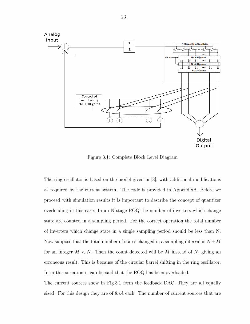
In this chapter the model given in Chapter 2 is verified and a circuit implementation
of the complete ADC (except for the output decimator) is presented. First a complete
VerilogA model is built, and then (step by step) the various components are replaced
by their schematics.
3.1 Behavioral Model
A VerilogA model of the ∆∑
ADC is developed based on the block diagram shown
in Fig.3.1
22
23
Figure 3.1: Complete Block Level Diagram
The ring oscillator is based on the model given in [8], with additional modifications
as required by the current system. The code is provided in AppendixA. Before we
proceed with simulation results it is important to describe the concept of quantizer
overloading in this case. In an N stage ROQ the number of inverters which change
state are counted in a sampling period. For the correct operation the total number
of inverters which change state in a single sampling period should be less than N.
Now suppose that the total number of states changed in a sampling interval is N+M
for an integer M < N . Then the count detected will be M instead of N , giving an
erroneous result. This is because of the circular barrel shifting in the ring oscillator.
In in this situation it can be said that the ROQ has been overloaded.
The current sources show in Fig.3.1 form the feedback DAC. They are all equally
sized. For this design they are of 8nA each. The number of current sources that are
24
switched on depends on the number of inverters which have changed state during the
previous sampling period. The current sources are controlled directly by the digital
output of the XOR gates. The number of inverters that change state is proportional
to the input current. For this design 13 inverters are used in the ring. The DAC
is calibrated such that when 5 inverters change state, the output current from the
DAC is zero. When more than 5 inverters change state, the output current is greater
than zero and vice versa. It could be said that in the feedback configuration the free
running frequency of this oscillator is such that 5 to 6 inverters change stage during a
sampling period. Here free running frequency is not used in a true sense but is used
because when the analog input of the ADC is zero, the ROQ is forced to oscillate at a
frequency such that the current from the feedback DAC is also zero. It is interesting
to note the similarities between this ADC and a Phase Locked Loop (PLL). In the
PLL the oscillator is forced to oscillate at a multiple of the input frequency through
a feedback. Structural similarities are also present and the main structural difference
is that in the PLL, at the input summing node, the difference taken is between the
phase of the input signal and the phase of the feedback signal. On the other in this
ADC, at the input summing node, the phase information of the feedback signal is
first converted to a current value and then subtracted from the input signal.
For this design, 5 inverter changing states correspond to zero current from the DAC
and it can go up to 13 inverters changing state in a sampling period. Since each
current cell in the DAC is equal to 8nA then the positive going current that the DAC
can provide is (13 − 5) ∗ 8nA = 64nA. Similarly from 5 inverters down to a delay of
0 zero inverters changing state, the negative going current that the DAC can provide
is (5 − 0)8nA = 40nA. To keep symmetry in the positive and negative cycles of the
DAC output current, we take that the maximum output of the DAC from +40nA to
−40nA. Since the analog input to the ADC is differential, a complementary copy of
25
this current is made so to have a differential output DAC, with a differential swing
from +80nA to −80nA. Hence 160nA is our full scale value. The amplitude of the
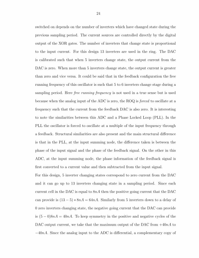
test signal in the rest of this thesis will be given relative to a full scale value of 160nA.
The results of this full VerilogA ∆∑
ADC are shown in Fig.3.2
10−4
10−3
10−2
10−1
100
−160
−140
−120
−100
−80
−60
−40
−20
0
20
Normalized Frequency
dB
FS
/NB
W
SNDR 54dB
Signal Bandwidthfs/2
Figure 3.2: Power Spectral Density of the VerilogA model of the ∆∑
ADC.Input:-12dBFS, 2.75KHz, Bandwidth: 25KHz, Sampling frequency: 1.024MHz
The signal frequency, bandwidth and the half of sampling frequency are marked by
vertical lines. The x-axis is normalized with respect to the sampling frequency. The
Power Spectral Density (PSD) validates the model that we had in the previous chapter
which resulted in a second order noise shaping to the quantization noise. A 40dB
per decade slope line is added on the PSD to increase the observability of the second
order noise shaping.
As seen in Fig.3.3, there is no difference between SNR and SNDR, because this is
an ideal model and there are no distortions due to circuit non-linearities. Whereas
Fig.3.4 is plotted using a non-linear tuning curve for the oscillator as given in (??).
This non-linear tuning curve has second and third order harmonics. And due to these

26
−80 −70 −60 −50 −40 −30 −20 −10 0−10
0
10
20
30
40
50
60
70
Input (dBFS)
Ou
tpu
t(d
B)
SNRSNDR
Figure 3.3: SNR and SNDR vs Input amplitude
non-linearities the SNDR drops below SNR for values of input above −9dBFS.
−80 −70 −60 −50 −40 −30 −20 −10 0−20
−10
0
10
20
30
40
50
60
70
Input Amplitude (dBFS)
Ou
tpu
t (d
B)
SNRSNDR
Figure 3.4: SNR and SNDR vs Input amplitude for a non-linear frequency tuningcurve
27
3.2 Ring Oscillator Quantizer
In this section a single inverter using Source Coupled Logic (SCL) is developed, and
its characteristics are discussed. This inverter is then used in a 13-stage ring oscillator.
3.2.1 Inverter Cell for ROQ
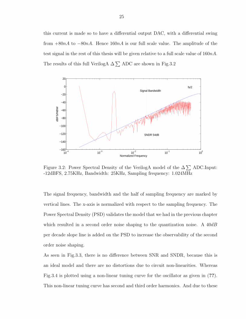
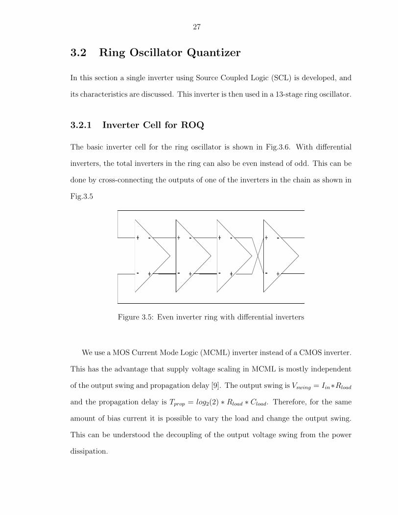
The basic inverter cell for the ring oscillator is shown in Fig.3.6. With differential
inverters, the total inverters in the ring can also be even instead of odd. This can be
done by cross-connecting the outputs of one of the inverters in the chain as shown in
Fig.3.5
Figure 3.5: Even inverter ring with differential inverters
We use a MOS Current Mode Logic (MCML) inverter instead of a CMOS inverter.
This has the advantage that supply voltage scaling in MCML is mostly independent
of the output swing and propagation delay [9]. The output swing is Vswing = Iin∗Rload
and the propagation delay is Tprop = log2(2) ∗ Rload ∗ Cload. Therefore, for the same
amount of bias current it is possible to vary the load and change the output swing.
This can be understood the decoupling of the output voltage swing from the power
dissipation.
28
Figure 3.6: Inverter Cell for the Ring Oscillator
The swing at the output node should be high enough to switch the next inverter
in the ring. For subthreshold operation the swing should be greater than 4nUt[10],
where n is the subthreshold slope factor and Ut is the thermal voltage given by kT/q.
Assuming n = 1.5, at room temperature the minimum swing should be greater than
150mV . So if we have a bias current of 100nA, this would require the load resistance
to be in the mega ohm range to ensure the switching of the next stage in the ring
oscillator. To implement this type of high value loads with easily tunable impedance
values, a PMOS load device is used with the bulk connected to the drain instead of
the source [11].
29
Figure 3.7: PMOS bulk-drain connected load for inverter cell
If the PMOS load is in subthreshold region then according to the EKV model the
drain to source current is given as
Isd = Io exp
(VBG − VTo
nPUT
)(exp
(−VBS
UT
)− exp
(−VBD
UT
))(3.1)
Therefore, for the load shown in Fig.3.7 VBD = 0. With this condition it can be easily
shown that the source drain resistance of this load device is [12]
RSD =
(∂ISD∂VSD
)−1=
(nPUT
Ib
)((nP − 1) exp
((nP − 1)υSD
)+ exp(−υSD)
)−1(3.2)
Where Ib = I0 exp(
VSG−VT0
nPUT
)and υSD = VSD
nPUTso the source drain resistance can
be controlled by the gate to source voltage. This is important because when the
input current to the oscillator changes, the resistance through a feedback loop can
be changed as well. Such that the current-resistance product remains constant. This
will ensure the same voltage swing at the output for a full range of currents. This
is important because according to Eqn.3.8, the frequency of oscillations depends on
the input current and the output swing. But for this system the output frequency
should provide quantized information about the input current only, thus the need for
30
constant output voltage swing so as to make the change in frequency of oscillation
dependent only on the input current.
3.2.2 Sustained Oscillations
According to Barkhausen stability criterion, a negative feedback circuit is stable if
the loop gain at a phase shift of 180o is less than one. But for this case oscillations
are needed for proper operation. In the ring oscillator, the transfer function of each
element can be written as H(s) = − A0
(1+s/ω0)[13]. In this thesis a 13 inverter ring
oscillator is used thus the loop gain for this ring oscillator can be written as
H(s) = − A130
(1 + s/ω0)13 (3.3)
The total frequency dependent phase shift should be 1800, so the phase shift per
stage should be 1800/13 = 13.840
tan−1 (ωosc/ω0) = 1800/13 = 13.840 (3.4)
ωosc = 0.246ω0 (3.5)
ωosc is the frequency at which the desired frequency dependent phase shift is
obtained, where ω0 is the 3−dB bandwidth of the inverter cell. The voltage gain per
stage required to ensure that the loop gain at ωosc is greater than 1 is
A130(√
1 +(
ωosc
ω0
)2)13 = 1 (3.6)
and for the case of ωosc = 0.246ω0,
31
A0 = 1.029 (3.7)
The magnitude and phase response of a single inverter cell are shown in Fig.3.8. From
the magnitude plot it is clear that the low frequency gain per stage is indeed greater
than the value given in 3.7.
Figure 3.8: Magnitude and Phase response of a single inverter cell of the ring oscillator
As explained in [13], ωosc is the frequency derived from the small signal characteristics
of the circuit, and it is the frequency at which the ring initially oscillates. As the
oscillations grow the circuit behaves in a non-linear fashion and the amplitude of the
output waveform is then limited by the design factors. When the amplitude of the
output saturates, the frequency of oscillation is then no more ωosc. According to [7]
the frequency of oscillation of an N element ring is given as
fosc =ISS
2.log2 (2) .N.Vsw.CL
(3.8)
Where Vsw is the output voltage swing, CL is the load capacitance and ISS is the tail
32
current. This result can be reached by considering that the period of oscillation is
2N times the propagation delay of a single inverter.
Tperiod = 2Nτd (3.9)
Where,
τd = log2 (2)Rload.CL (3.10)
and
Rload =VswISS
(3.11)
3.2.3 Inverter Cell with Replica Bias and Input Current Mir-
ror
A cascode of NMOS transistors with gain boosting is used for the tail as shown in
Fig.3.9(b). This figure also shows the the use of special drain-bulk connected loads.
Type Transistors W/L
NMOSM1, M2, M11 480/180 nmM5, M7, M10 5/2 µmM6, M8, M9 2/5 µm
PMOS M3, M4, M12 4/4 µm
The voltage VbiasP is provided through the feedback loop as shown in Fig.3.9(a).
This ensures the dynamic changing of the PMOS load resistance, to ensure that the
current-resistance product at the output node stays constant. Voltage Vswing is the
lower value of the output swing. In this case VDD is 0.8V and the output voltage
has a swing (Vswing) of 300mV . At the schematic level, a load capacitance of 100fF
is also added at the output node to simulate the effects of the parasitic capacitance
present when layout is done, due to the interconnects between inverters and the FDC.
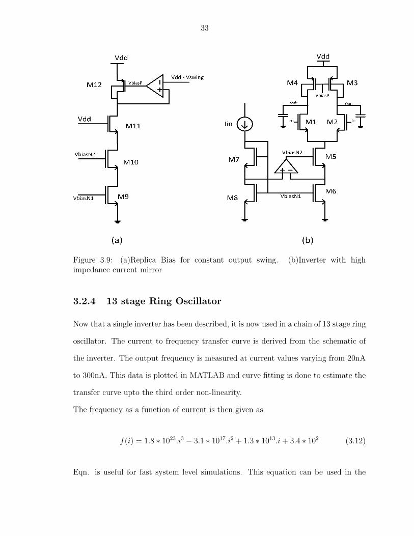
33
Figure 3.9: (a)Replica Bias for constant output swing. (b)Inverter with highimpedance current mirror
3.2.4 13 stage Ring Oscillator
Now that a single inverter has been described, it is now used in a chain of 13 stage ring
oscillator. The current to frequency transfer curve is derived from the schematic of
the inverter. The output frequency is measured at current values varying from 20nA
to 300nA. This data is plotted in MATLAB and curve fitting is done to estimate the
transfer curve upto the third order non-linearity.
The frequency as a function of current is then given as
f(i) = 1.8 ∗ 1023.i3 − 3.1 ∗ 1017.i2 + 1.3 ∗ 1013.i+ 3.4 ∗ 102 (3.12)
Eqn. is useful for fast system level simulations. This equation can be used in the
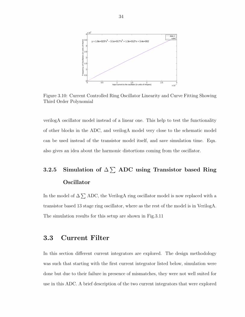
34
0 0.5 1 1.5 2 2.5 3
x 10−7
0
0.5
1
1.5
2
2.5
3
3.5
4x 10
5
Input current to the oscillator (in units of Ampere)F
req
ue
ncy
of
Osc
illa
tion
(in
un
its o
f H
ert
z)
y = 1.8e+023*x3 − 3.1e+017*x2 + 1.3e+012*x + 3.4e+002
data 1 cubic
Figure 3.10: Current Controlled Ring Oscillator Linearity and Curve Fitting ShowingThird Order Polynomial
verilogA oscillator model instead of a linear one. This help to test the functionality
of other blocks in the ADC, and verilogA model very close to the schematic model
can be used instead of the transistor model itself, and save simulation time. Eqn.
also gives an idea about the harmonic distortions coming from the oscillator.
3.2.5 Simulation of ∆∑
ADC using Transistor based Ring
Oscillator
In the model of ∆∑
ADC, the VerilogA ring oscillator model is now replaced with a
transistor based 13 stage ring oscillator, where as the rest of the model is in VerilogA.
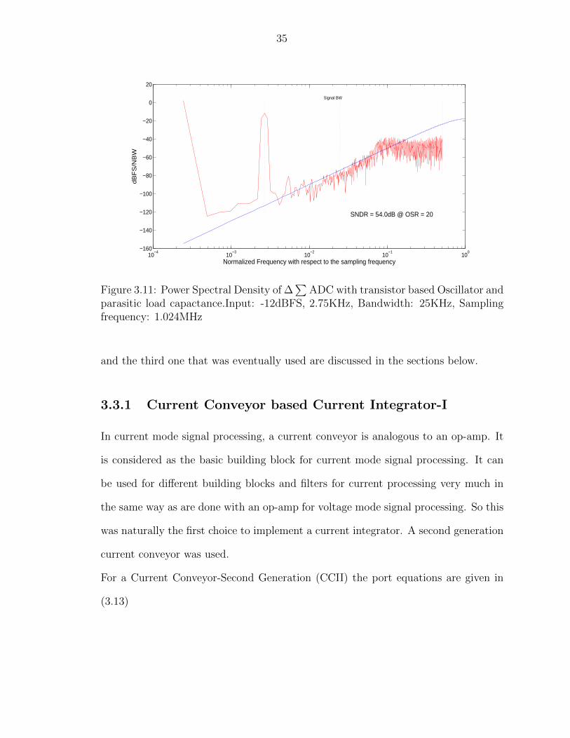
The simulation results for this setup are shown in Fig.3.11
3.3 Current Filter
In this section different current integrators are explored. The design methodology
was such that starting with the first current integrator listed below, simulation were
done but due to their failure in presence of mismatches, they were not well suited for
use in this ADC. A brief description of the two current integrators that were explored
35
10−4
10−3
10−2
10−1
100
−160
−140
−120
−100
−80
−60
−40
−20
0
20
Normalized Frequency with respect to the sampling frequency
dB
FS
/NB
W
SNDR = 54.0dB @ OSR = 20
Signal BW
Figure 3.11: Power Spectral Density of ∆∑
ADC with transistor based Oscillator andparasitic load capactance.Input: -12dBFS, 2.75KHz, Bandwidth: 25KHz, Samplingfrequency: 1.024MHz
and the third one that was eventually used are discussed in the sections below.
3.3.1 Current Conveyor based Current Integrator-I
In current mode signal processing, a current conveyor is analogous to an op-amp. It
is considered as the basic building block for current mode signal processing. It can
be used for different building blocks and filters for current processing very much in
the same way as are done with an op-amp for voltage mode signal processing. So this
was naturally the first choice to implement a current integrator. A second generation
current conveyor was used.
For a Current Conveyor-Second Generation (CCII) the port equations are given in
(3.13)
36
Figure 3.12: Current Conveyor symbol
Iy
Vx
Iz
=
0 0 0
1 0 0
0 ±1 0
×
Vy
Ix
Vz
(3.13)
This means that the voltage Vx should follow the voltage Vy. The current into or
out of node X is equal to the current into or out of node Z. Although at circuit level
the relation can be adjusted such that Iz = αIx, where α can also be any value other
than one. These characteristics also determine the impedance looking into each of
these ports. Ideally, the impedance looking into Y and Z should be very high and
looking into X it should be very low. A typical construction of a CCII is shown in
Fig.3.13. Many other implementations can be found in [14].
The integrator needed for the design of this specific ADC has to have differential
input and single ended output. One such implementation given in [15], is shown in
Fig.3.14
Keeping in view the CCII port relations given in the matrix, it can be easily derived
for the Fig.3.14 that,
Iout =(I2 − I1)
sCR1
(3.14)
This circuit was implemented in the subthreshold region to save on power consump-
tion. It gave results close to the simulated values but when Montecarlo simulations
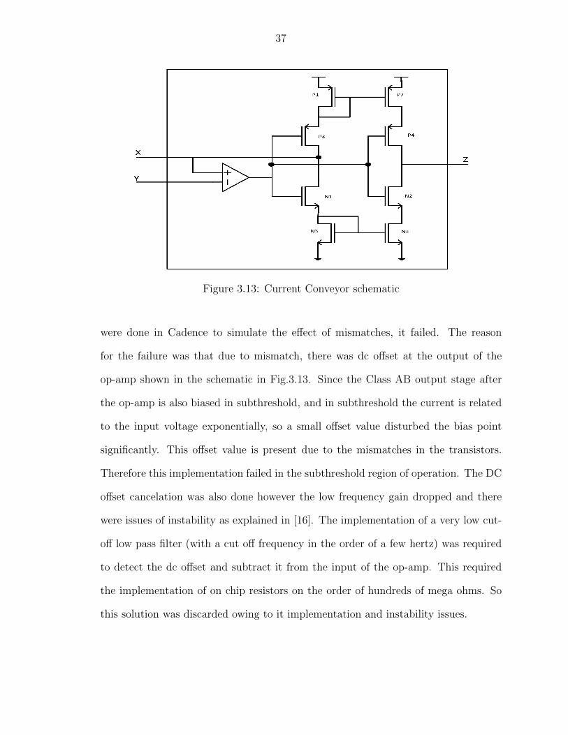
37
Figure 3.13: Current Conveyor schematic
were done in Cadence to simulate the effect of mismatches, it failed. The reason
for the failure was that due to mismatch, there was dc offset at the output of the
op-amp shown in the schematic in Fig.3.13. Since the Class AB output stage after
the op-amp is also biased in subthreshold, and in subthreshold the current is related
to the input voltage exponentially, so a small offset value disturbed the bias point
significantly. This offset value is present due to the mismatches in the transistors.
Therefore this implementation failed in the subthreshold region of operation. The DC
offset cancelation was also done however the low frequency gain dropped and there
were issues of instability as explained in [16]. The implementation of a very low cut-
off low pass filter (with a cut off frequency in the order of a few hertz) was required
to detect the dc offset and subtract it from the input of the op-amp. This required
the implementation of on chip resistors on the order of hundreds of mega ohms. So
this solution was discarded owing to it implementation and instability issues.

38
Figure 3.14: Current Conveyor based current integrator
3.3.2 Current Integrator-II
The second current integrator that was investigated is from [17]. The working prin-
cipal is based on the current integrator given in [18]. For simplicity the integrator in
[18] is shown in Fig.3.15 and it is used to explain why this option was not pursued
further.
Figure 3.15: Second Integrator: Mismatches between M1 and M4 cause a large biascurrent variation if the transistors are in subthreshold
The transfer function for this circuits as given in [18] is Iout = gm(Ip−In)sC
assuming all
the transistors have same W/L. Now in the presence of mismatch between M1 and M4,
39
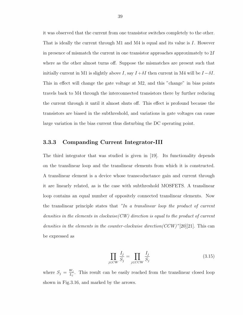
it was observed that the current from one transistor switches completely to the other.
That is ideally the current through M1 and M4 is equal and its value is I. However
in presence of mismatch the current in one transistor approaches approximately to 2I
where as the other almost turns off. Suppose the mismatches are present such that
initially current in M1 is slightly above I, say I+δI then current in M4 will be I−δI.
This in effect will change the gate voltage at M2, and this ”change” in bias points
travels back to M4 through the interconnected transistors there by further reducing
the current through it until it almost shuts off. This effect is profound because the
transistors are biased in the subthreshold, and variations in gate voltages can cause
large variation in the bias current thus disturbing the DC operating point.
3.3.3 Companding Current Integrator-III
The third integrator that was studied is given in [19]. Its functionality depends
on the translinear loop and the translinear elements from which it is constructed.
A translinear element is a device whose transcoductance gain and current through
it are linearly related, as is the case with subthreshold MOSFETS. A translinear
loop contains an equal number of oppositely connected translinear elements. Now
the translinear principle states that ”In a translinear loop the product of current
densities in the elements in clockwise(CW) direction is equal to the product of current
densities in the elements in the counter-clockwise direction(CCW)”[20][21]. This can
be expressed as
∏j∈CW
IjSj
=∏
j∈CCW
IjSj
(3.15)
where Sj =Wj
Lj. This result can be easily reached from the translinear closed loop
shown in Fig.3.16, and marked by the arrows.

40
Figure 3.16: An example of a translinear loop
For this loop we can write
Vgs1 + Vgs2 = Vgs3 + Vgs4 (3.16)
Since they are in subthreshold region then from [10] we can write
ln
(ID1
Ispec1
)+ ln
(ID2
Ispec2
)= ln
(ID3
Ispec3
)+ ln
(ID4
Ispec4
)(3.17)
where IspecN = 2nµCoxU2T
(WL
)N
. Ideally 2nµCoxU2T will be the same for the transis-
tors, so in this case
ID1(WL
)1
ID2(WL
)2
=ID3(WL
)3
ID4(WL
)4
(3.18)
Based on the differential BJT circuit given in [19], the corresponding MOSFET
circuit is shown in Fig.3.17
The arrows mark the elements forming the translinear loop for one side of the differ-
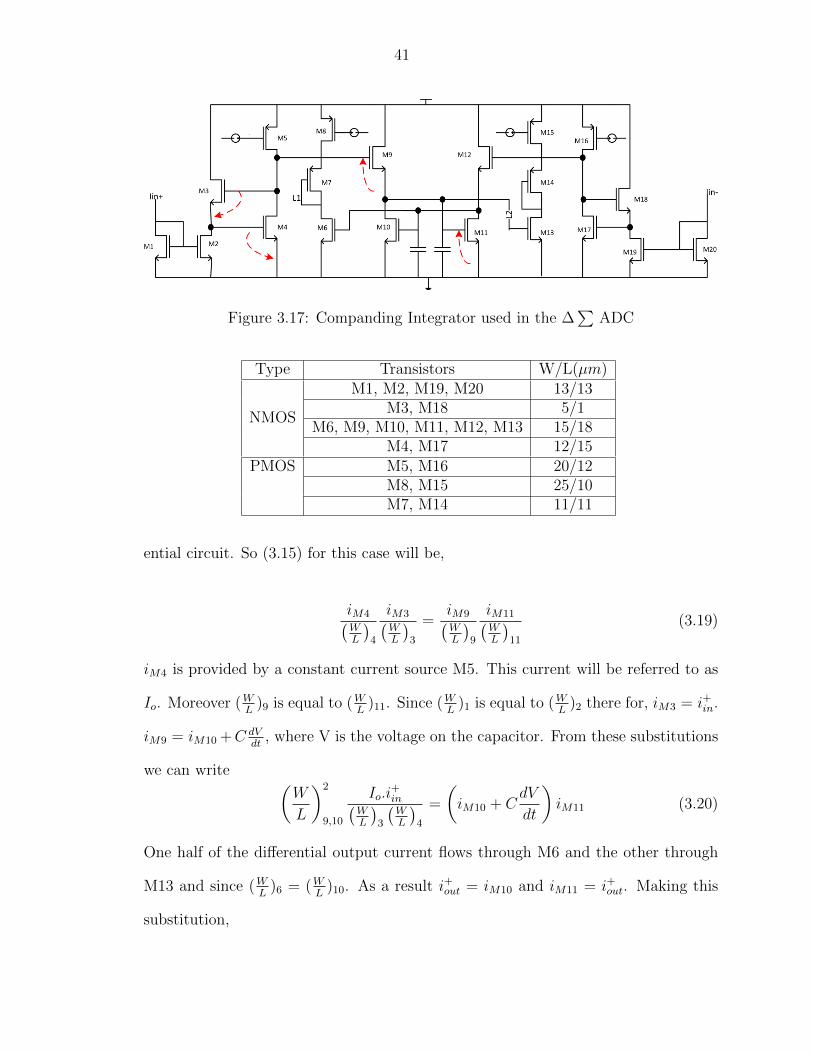
41
Figure 3.17: Companding Integrator used in the ∆∑
ADC
Type Transistors W/L(µm)
NMOS
M1, M2, M19, M20 13/13M3, M18 5/1
M6, M9, M10, M11, M12, M13 15/18M4, M17 12/15
PMOS M5, M16 20/12M8, M15 25/10M7, M14 11/11
ential circuit. So (3.15) for this case will be,
iM4(WL
)4
iM3(WL
)3
=iM9(WL
)9
iM11(WL
)11
(3.19)
iM4 is provided by a constant current source M5. This current will be referred to as
Io. Moreover (WL
)9 is equal to (WL
)11. Since (WL
)1 is equal to (WL
)2 there for, iM3 = i+in.
iM9 = iM10 +C dVdt
, where V is the voltage on the capacitor. From these substitutions
we can write (W
L
)2
9,10
Io.i+in(
WL
)3
(WL
)4
=
(iM10 + C
dV
dt
)iM11 (3.20)
One half of the differential output current flows through M6 and the other through
M13 and since (WL
)6 = (WL
)10. As a result i+out = iM10 and iM11 = i+out. Making this
substitution,
42
(W
L
)2
9,10
Io.i+in(
WL
)3
(WL
)4
=
(i−out + C
dV
dt
)i+out (3.21)
Similarly for the other half of the differential circuit,
(W
L
)2
9,10
Io.i−in(
WL
)3
(WL
)4
=
(i+out + C
dV
dt
)i−out (3.22)
Let (WL
)29,10(
WL
)3
(WL
)4
= K (3.23)
Then subtracting (3.22) from (3.21) the following is obtained
K.Io(i+in − i−in
)=(i+out − i−out
).CdV
dt(3.24)
Or simply:
K.I0C
.iindt = ioutdV (3.25)
Since the transistors are in subthreshold, we ca write
iout = ISpec.eVgs−Vth
nVT (3.26)
where Vgs at the same time is the capacitor voltage V. Putting (3.26) in (3.25) and
integrating the following can be obtained
iout =KIonCVT
∫iindt (3.27)
The output current from this integrator goes into the oscillator. The input to the
oscillator is single ended. To convert the differential output current to the single

43
ended equivalent the circuit shown in Fig.3.18 is used.
Figure 3.18: Differential to single ended conversion
Type Transistors W/LNMOS M13 1 15/18 µmPMOS M7 1 11/11 µm
The L1 and L2 nodes in Fig.3.18 are connected to the L1 and L2 nodes in Fig.3.17.
3.3.4 Simulation Result
Here the results of simulation of the ∆∑
ADC using the transistor based integrator
is presented.
44
−80 −70 −60 −50 −40 −30 −20 −10 0−10
0
10
20
30
40
50
60
Input(dBFS)
Ou
tpu
t(d
B)
SNR
SNDR
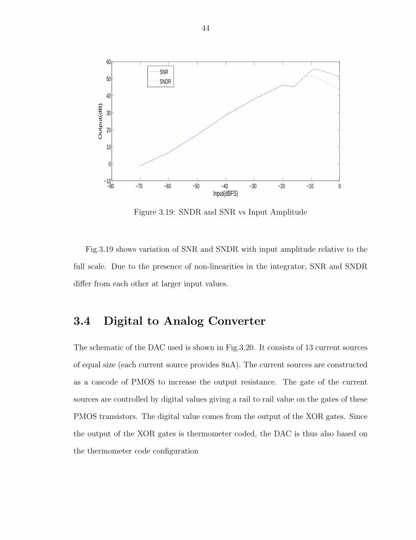
Figure 3.19: SNDR and SNR vs Input Amplitude
Fig.3.19 shows variation of SNR and SNDR with input amplitude relative to the
full scale. Due to the presence of non-linearities in the integrator, SNR and SNDR
differ from each other at larger input values.
3.4 Digital to Analog Converter
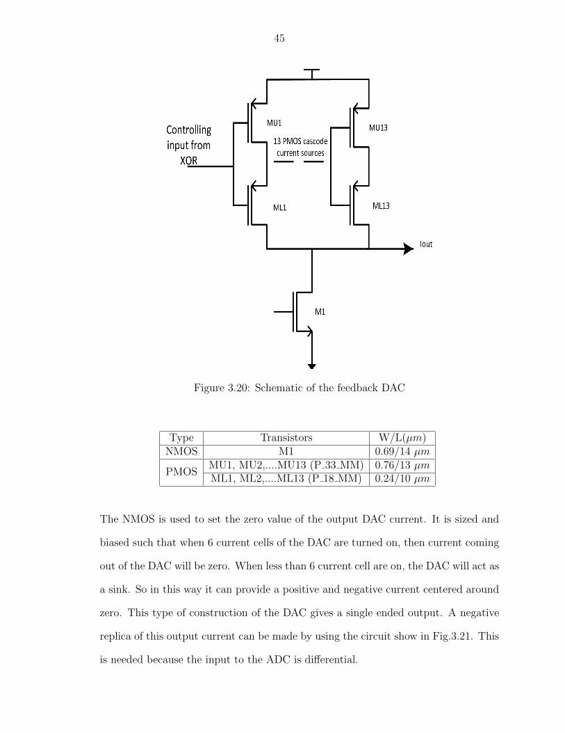
The schematic of the DAC used is shown in Fig.3.20. It consists of 13 current sources
of equal size (each current source provides 8nA). The current sources are constructed
as a cascode of PMOS to increase the output resistance. The gate of the current
sources are controlled by digital values giving a rail to rail value on the gates of these
PMOS transistors. The digital value comes from the output of the XOR gates. Since
the output of the XOR gates is thermometer coded, the DAC is thus also based on
the thermometer code configuration
45
Figure 3.20: Schematic of the feedback DAC
Type Transistors W/L(µm)NMOS M1 0.69/14 µm
PMOSMU1, MU2,....MU13 (P 33 MM) 0.76/13 µmML1, ML2,....ML13 (P 18 MM) 0.24/10 µm
The NMOS is used to set the zero value of the output DAC current. It is sized and
biased such that when 6 current cells of the DAC are turned on, then current coming
out of the DAC will be zero. When less than 6 current cell are on, the DAC will act as
a sink. So in this way it can provide a positive and negative current centered around
zero. This type of construction of the DAC gives a single ended output. A negative
replica of this output current can be made by using the circuit show in Fig.3.21. This
is needed because the input to the ADC is differential.

46
Figure 3.21: Circuit to create a Negative Replica of the DAC Output Current. (WL
=0.2413µm for all transistors)
3.4.1 Data Weighted Averaging
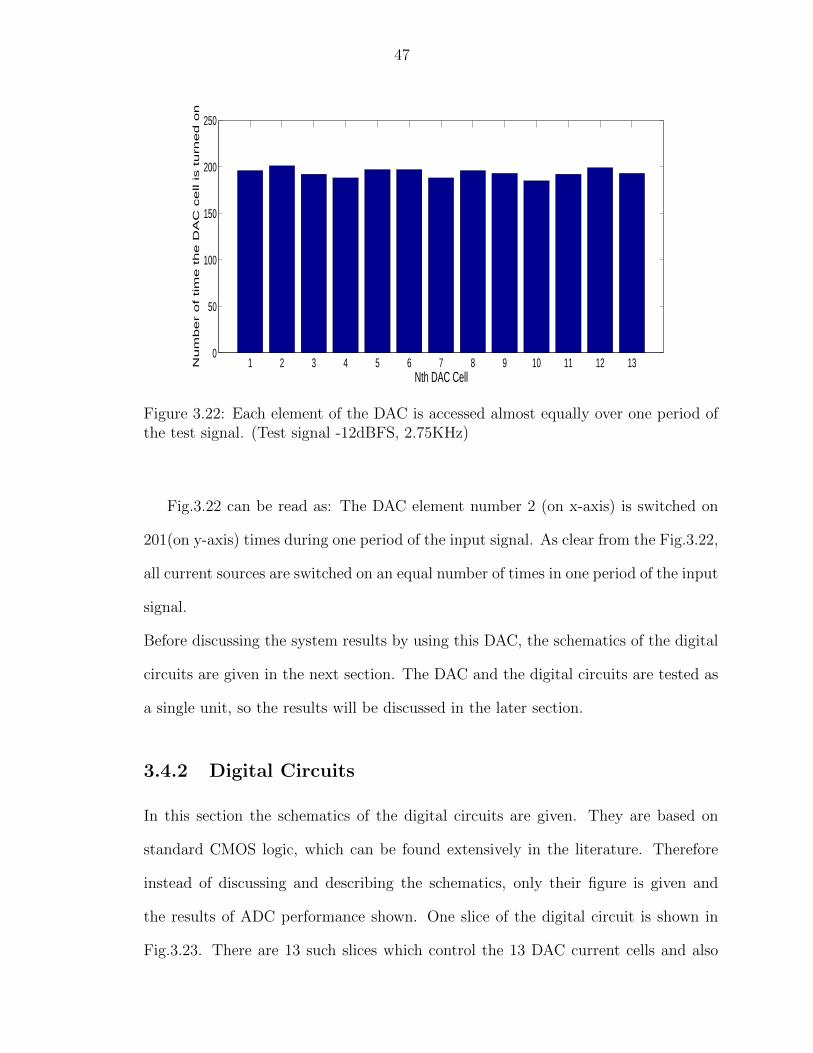
The concept of inherent DWA is presented in previous chapter. In this section its
results. A -12dBFS input at 2.75KHz was used as the test signal. The number of
times each DAC cell is switched on during one period of the input signal is counted.
This count is plotted on the y-axis of Fig.3.22 and the DAC cell number on the x-axis.
47
1 2 3 4 5 6 7 8 9 10 11 12 130
50
100
150
200
250
Nth DAC Cell
Num
ber
of tim
e the D
AC
cell is turn
ed o
n
Figure 3.22: Each element of the DAC is accessed almost equally over one period ofthe test signal. (Test signal -12dBFS, 2.75KHz)
Fig.3.22 can be read as: The DAC element number 2 (on x-axis) is switched on
201(on y-axis) times during one period of the input signal. As clear from the Fig.3.22,
all current sources are switched on an equal number of times in one period of the input
signal.
Before discussing the system results by using this DAC, the schematics of the digital
circuits are given in the next section. The DAC and the digital circuits are tested as
a single unit, so the results will be discussed in the later section.
3.4.2 Digital Circuits
In this section the schematics of the digital circuits are given. They are based on
standard CMOS logic, which can be found extensively in the literature. Therefore
instead of discussing and describing the schematics, only their figure is given and
the results of ADC performance shown. One slice of the digital circuit is shown in
Fig.3.23. There are 13 such slices which control the 13 DAC current cells and also
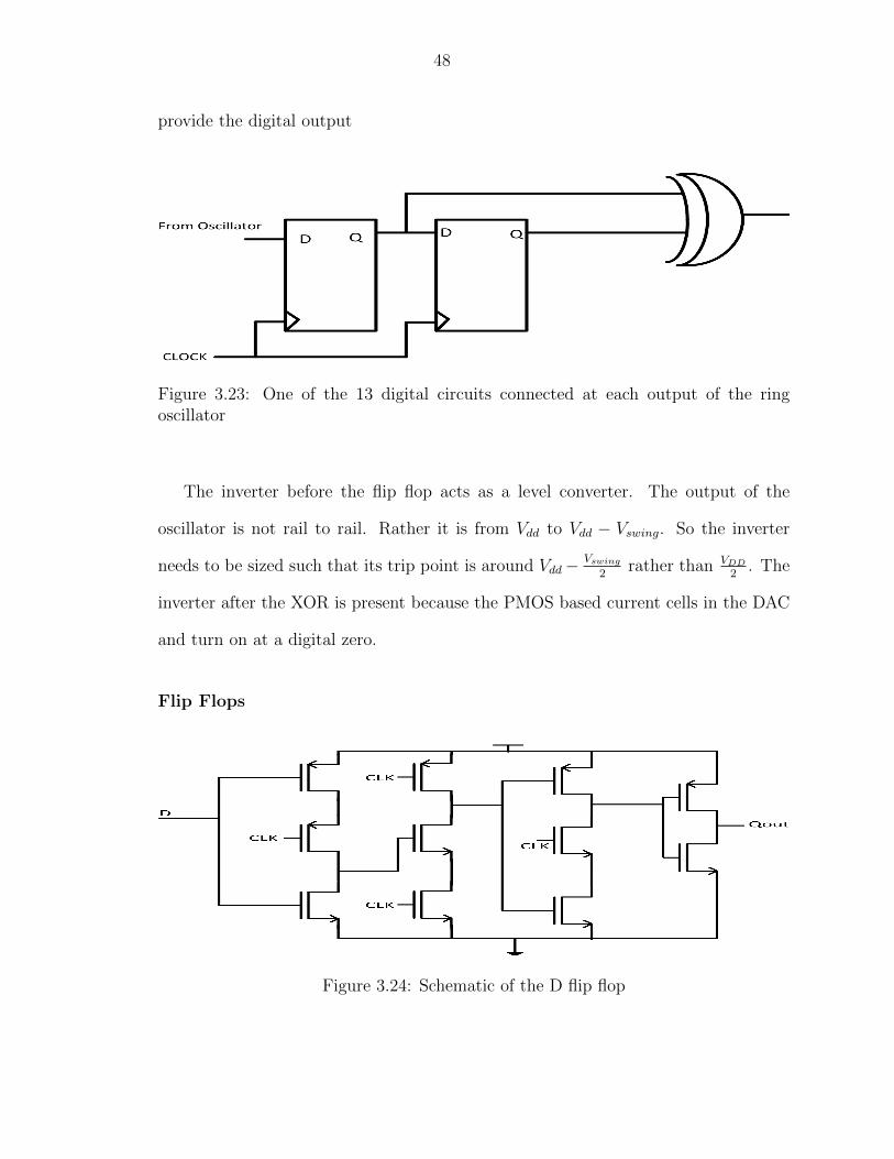
48
provide the digital output
Figure 3.23: One of the 13 digital circuits connected at each output of the ringoscillator
The inverter before the flip flop acts as a level converter. The output of the
oscillator is not rail to rail. Rather it is from Vdd to Vdd − Vswing. So the inverter
needs to be sized such that its trip point is around Vdd − Vswing
2rather than VDD
2. The
inverter after the XOR is present because the PMOS based current cells in the DAC
and turn on at a digital zero.
Flip Flops
Figure 3.24: Schematic of the D flip flop

49
XOR Gates
Figure 3.25: Schematic of the D flip flop
3.4.3 Simulation Results using Transistor Model for DAC
and Digital Circuits
The simulation time increases considerably when the transistor based model is intro-
duced for the digital circuits. Thus instead of plotting the SNDR variation with the
input amplitude (for which multiple runs are required) just one simulation was done.
50
10−4
10−3
10−2
10−1
100
−140
−120
−100
−80
−60
−40
−20
0
20
Normalized Frequency
dB
FS
/NB
W
PSD for verilog based DAC and Digital CircuitsPSD for transistor based DAC and Digital Circuits
Figure 3.26: Power Spectral Density of VerilogA based DAC and digital Circuits vsTransistor Based DAC and Digital Circuits(while the rest of the model is in VerilogA)
The test conditions were -12dBFS, 2.75KHz. For VerilogA model the SNDR is
54.3dB and for the transistor model the SNDR is 53dB The in band noise floor is
raised as compared to the VerilogA model. This is because to reduce the effects of
mismatches, the current mirrors at the output of the DAC are very large, thereby
increasing the parasitic capacitances. The output current from the DAC (on the order
of tens of nano amperes) when drive these capacitance its pulse shape gets distorted.
Which can increase the inband noise content.
3.5 OTAs for Replica Bias and Gain Boosted Cur-
rent Mirror
The schematics of the opamps used in the replica bias and the gain boosted current
mirror shown in Fig.3.9 for the oscillator are given in this section.
51
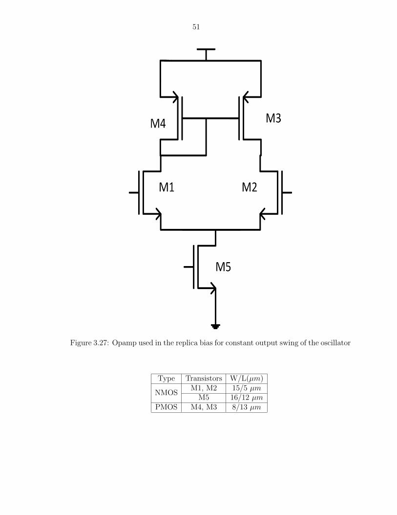
Figure 3.27: Opamp used in the replica bias for constant output swing of the oscillator
Type Transistors W/L(µm)
NMOSM1, M2 15/5 µm
M5 16/12 µmPMOS M4, M3 8/13 µm

52
Figure 3.28: Opamp used in the gain boosting of the current mirror input stage ofthe oscillator
Type Transistors W/L(µm)
PMOSM1, M2 10/5 µm
M5 16/13 µmNMOS M4, M3 2/15 µm

Chapter 4
Simulation Results - Evolution of
SNR/SNDR going from Behavioral
Model to Transistor Model
In this chapter the results are given step by step, that is starting from the verilogA
model, we insert the transistor level models one by one and compare the results. At
the end the MonteCarlo simulation results are also presented.
53
54
−80 −70 −60 −50 −40 −30 −20 −10 0−10
0
10
20
30
40
50
60
70
Input (dBFS)
Out
put(
dB)
SNRSNDR
Figure 4.1: SNR and SNDR vs input amplitude-Complete Behavioral Model
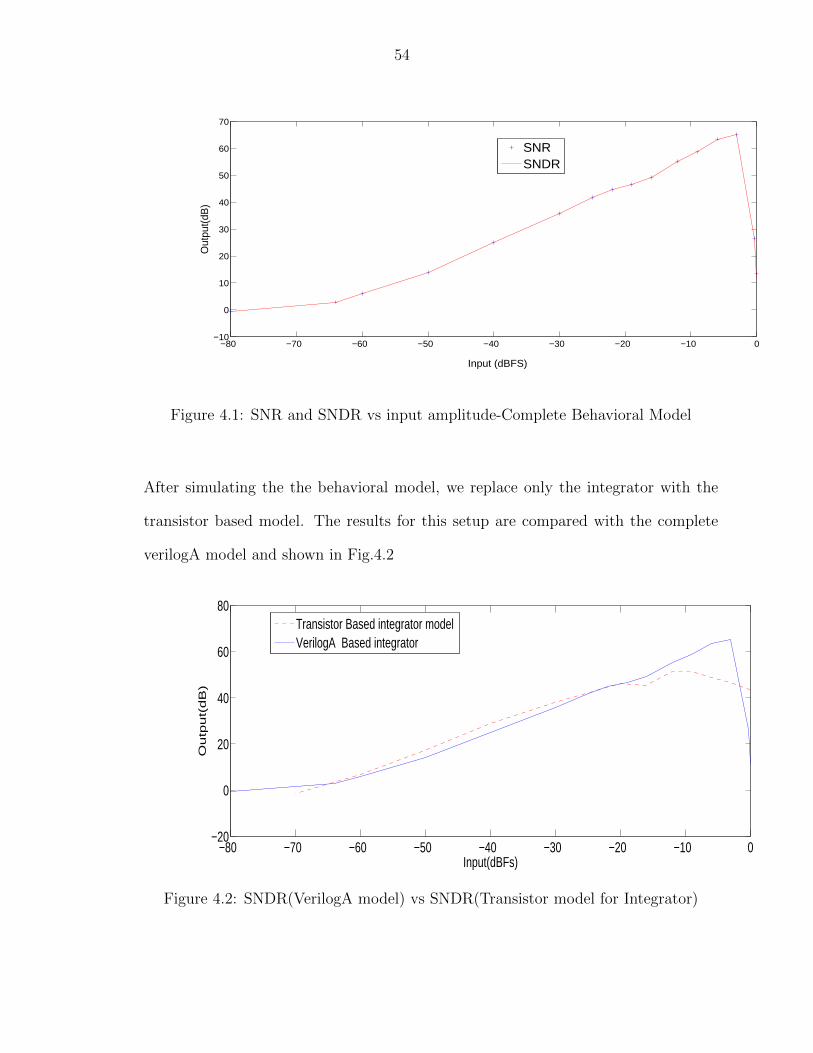
After simulating the the behavioral model, we replace only the integrator with the
transistor based model. The results for this setup are compared with the complete
verilogA model and shown in Fig.4.2
−80 −70 −60 −50 −40 −30 −20 −10 0−20
0
20
40
60
80
Input(dBFs)
Ou
tpu
t(d
B)
Transistor Based integrator modelVerilogA Based integrator
Figure 4.2: SNDR(VerilogA model) vs SNDR(Transistor model for Integrator)
55
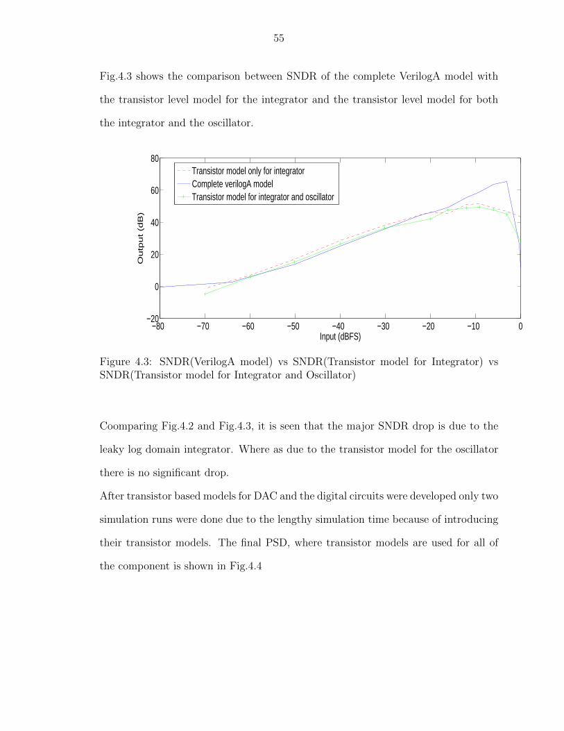
Fig.4.3 shows the comparison between SNDR of the complete VerilogA model with
the transistor level model for the integrator and the transistor level model for both
the integrator and the oscillator.
−80 −70 −60 −50 −40 −30 −20 −10 0−20
0
20
40
60
80
Input (dBFS)
Ou
tpu
t (d
B)
Transistor model only for integratorComplete verilogA modelTransistor model for integrator and oscillator
Figure 4.3: SNDR(VerilogA model) vs SNDR(Transistor model for Integrator) vsSNDR(Transistor model for Integrator and Oscillator)
Coomparing Fig.4.2 and Fig.4.3, it is seen that the major SNDR drop is due to the
leaky log domain integrator. Where as due to the transistor model for the oscillator
there is no significant drop.
After transistor based models for DAC and the digital circuits were developed only two
simulation runs were done due to the lengthy simulation time because of introducing
their transistor models. The final PSD, where transistor models are used for all of
the component is shown in Fig.4.4
56
10−4
10−3
10−2
10−1
100
−120
−100
−80
−60
−40
−20
0
20
Normalized Frequency w.r.t the sampling frequency
dB
FS
/NB
W
SNDR = 46.5dB @ OSR = 20Signal
SignalBandwidth
Figure 4.4: Power Spectral Density of the complete transistor model,SNR=51.2dB,SNDR = 46.4dB, Input: -9dBFs, 2.75KHz, Bandwidth 25KHz. Dynamic Range:54dB
In Fig.4.5, the digital output is plotted against a ramp input (in nanao-amps) upto
the full scale value. As mentioned in the previous sections, the digital output is 6
for an input current of 0 and above six for current above 0 and below 6 for current
values below zero. This can also be seen in the figure. The peak to peak value of the
input current which corresponds to -6dBFS and -12dBFS have also been marked on
the figure. For values of input current above -6dBFS, it can be seen that the digital
output losses its symmetry and hence the drop in SNR.
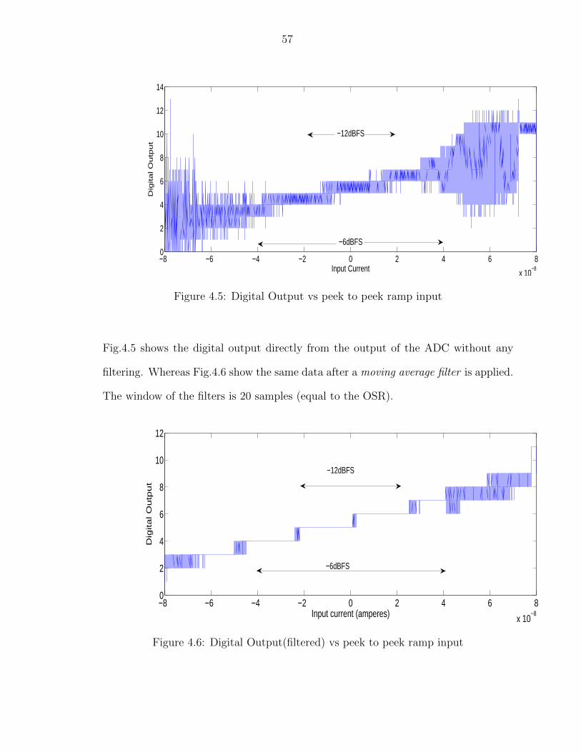
57
−8 −6 −4 −2 0 2 4 6 8
x 10−8
0
2
4
6
8
10
12
14
Input Current
Dig
ita
l O
utp
ut
−6dBFS
−12dBFS
Figure 4.5: Digital Output vs peek to peek ramp input
Fig.4.5 shows the digital output directly from the output of the ADC without any
filtering. Whereas Fig.4.6 show the same data after a moving average filter is applied.
The window of the filters is 20 samples (equal to the OSR).
−8 −6 −4 −2 0 2 4 6 8
x 10−8
0
2
4
6
8
10
12
Input current (amperes)
Dig
ita
l O
utp
ut
−6dBFS
−12dBFS
Figure 4.6: Digital Output(filtered) vs peek to peek ramp input
58
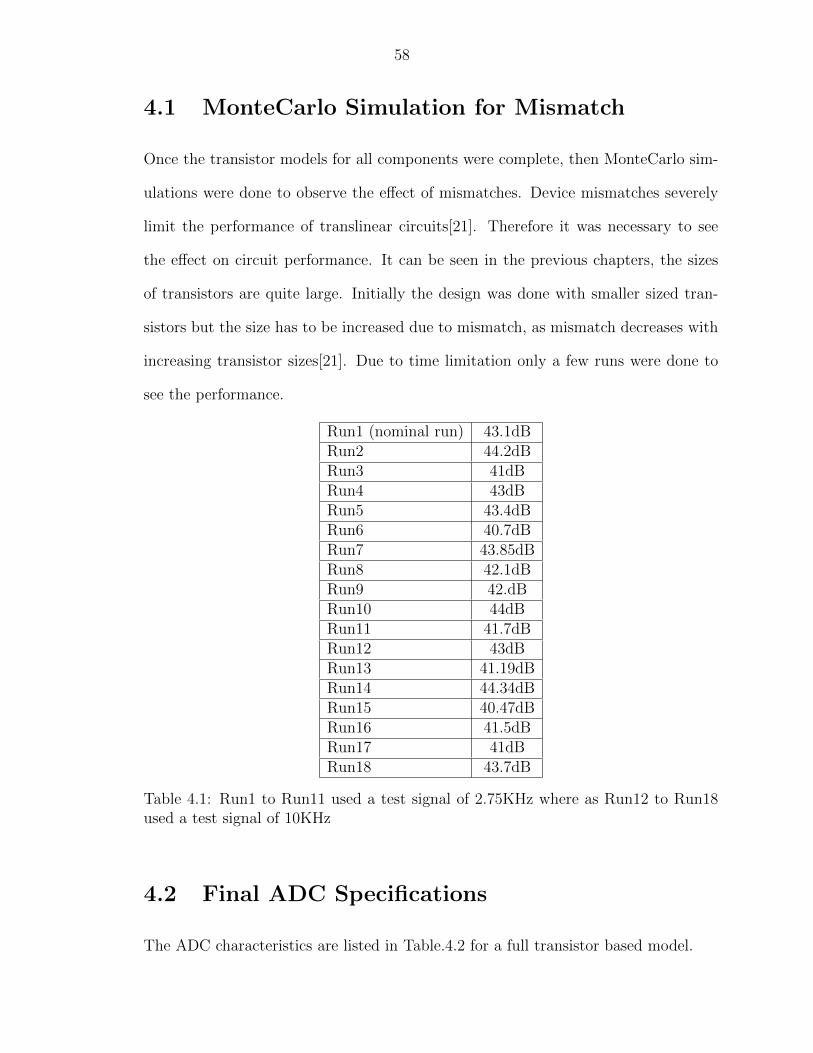
4.1 MonteCarlo Simulation for Mismatch
Once the transistor models for all components were complete, then MonteCarlo sim-
ulations were done to observe the effect of mismatches. Device mismatches severely
limit the performance of translinear circuits[21]. Therefore it was necessary to see
the effect on circuit performance. It can be seen in the previous chapters, the sizes
of transistors are quite large. Initially the design was done with smaller sized tran-
sistors but the size has to be increased due to mismatch, as mismatch decreases with
increasing transistor sizes[21]. Due to time limitation only a few runs were done to
see the performance.
Run1 (nominal run) 43.1dBRun2 44.2dBRun3 41dBRun4 43dBRun5 43.4dBRun6 40.7dBRun7 43.85dBRun8 42.1dBRun9 42.dBRun10 44dBRun11 41.7dBRun12 43dBRun13 41.19dBRun14 44.34dBRun15 40.47dBRun16 41.5dBRun17 41dBRun18 43.7dB
Table 4.1: Run1 to Run11 used a test signal of 2.75KHz where as Run12 to Run18used a test signal of 10KHz
4.2 Final ADC Specifications
The ADC characteristics are listed in Table.4.2 for a full transistor based model.

59
Technology UMC 180nmVdd 0.8 VPower Consumption 5.3µWSNR (@ -9dBFS, 25KHz BW) 51.2dBSNDR (@ -9dBFS, 25KHz BW) 46.4dBENOB 7.41Dynamic Range 54dBSampling Frequency 1.024MHzTHD 0.0015%SFDR 48.2dBFigure of Merit( power
2.BW.2ENOB ) 0.553pJ/Conversion (@ 30KHz BW)Figure of Merit( power
2.BW.2ENOB ) 0.612pJ/Conversion (@ 25KHz BW)
Table 4.2: ADC Specifications based on transistor modeling
4.3 Comparison with other state of the art CT-
∆∑
ADC
In the table.4.3, the Figure of Merit (FOM) used is power2.BW.2ENOB .
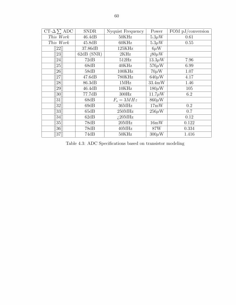
60
CT-∆∑
ADC SNDR Nyquist Frequency Power FOM pJ/conversionThis Work 46.4dB 50KHz 5.3µW 0.61This Work 45.8dB 60KHz 5.3µW 0.55
[[22]] 37.86dB 125KHz 6µW[[23]] 62dB (SNR) 2KHz ¡80µW[[24]] 72dB 512Hz 13.3µW 7.96[[25]] 68dB 40KHz 576µW 6.99[[26]] 58dB 100KHz 70µW 1.07[[27]] 47.6dB 780KHz 640µW 4.17[[28]] 86.3dB 1MHz 33.4mW 1.46[[29]] 46.4dB 10KHz 180µW 105[[30]] 77.7dB 300Hz 11.7µW 6.2[[31]] 68dB Fs = 3MHz 860µW[[32]] 69dB 36MHz 17mW 0.2[[33]] 65dB 250MHz 256µW 0.7[[34]] 62dB ¿20MHz 0.12[[35]] 78dB 20MHz 16mW 0.122[[36]] 78dB 40MHz 87W 0.334[[37]] 74dB 50KHz 300µW 1.416
Table 4.3: ADC Specifications based on transistor modeling
Chapter 5
Summary
5.1 Conclusion
In this thesis a low power current mode sigma delta ADC is presented for use with
frequencies upto 30KHz. This ADC can be used in battery operated bio-medical
devices due to its low power consumption. It can also be driectly interfaced with
sensors providing current output. Although it is currently designed in UMC 180nm
technology because of the manufacturing costs, but the technology can be easily
scaled down owing to it mostly digital nature. Montecarlo simulations are also done to
make the circuit more redundant to mismatches, as they can degrade the performance
specially in the subthreshold region. Since the main analog block is the log-domain
integrator, it is this block whihc is most sensitive to mismatches.
5.2 Future Work
This thesis involved design from VerilogA model down to the transistor model. The
future course of action can be to run a large number of montecarlo simulations to get
a better understanding of the effect of mismatches specially regarding the integrator.
61
62
Then a layout can be done with special techniques to reduce mismatch between
current mirrors. And finally a tape out. The design can be extended to higher
order loops for better SNR and SNDR. The integrator can be made more lossless to
improve the inband noise shaping. To increase the OSR, we will need to decrease
the parasitic capacitance (which is currently approximated by 100fF) at the output
of the oscillator. Because simply increasing the OSR will force a larger input current
to the oscillator which can cause non-linear distortions. So by increasing OSR and
reducing output capacitance, we can keep the magnitude of the biasing current the
same which was for the lower OSR. Further tests can be done to better characterize
the ADC.

APPENDICES

Appendix A
Appendix A Verilog-A Code for
Oscillator Model
//This is the verilog model of the oscillator based on [5] and [8].
‘include ”constants.vams” ‘include ”disciplines.vams” ‘define PI 3.14159
module CCRO(in,clk,sum out,Ioutp,Ioutn);
input in,clk; output sum out,Ioutp,Ioutn;
electrical in,sum out,Ioutp,Ioutn,clk;
parameter real fc=0,Kc=1.2e12;
parameter N=13;
real vout,fcco,phase,Ac,vmid;
real vcout[0:N-1];
integer q1[0:N-1],q2[0:N-1];
integer i,count,myseed;
analog begin
@(initial step) begin Ac = 150e-3; vmid=650e-3; myseed=233; end
fcco = Kc*I(in) + fc;
64
65
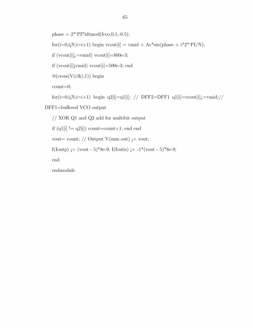
phase = 2*‘PI*idtmod(fcco,0,1,-0.5);
for(i=0;i¡N;i=i+1) begin vcout[i] = vmid + Ac*sin(phase + i*2*‘PI/N);
if (vcout[i]¿=vmid) vcout[i]=800e-3;
if (vcout[i]¡vmid) vcout[i]=500e-3; end
@(cross(V(clk),1)) begin
count=0;
for(i=0;i¡N;i=i+1) begin q2[i]=q1[i]; // DFF2=DFF1 q1[i]=vcout[i]¿=vmid;//
DFF1=buffered VCO output
// XOR Q1 and Q2 add for multibit output
if (q1[i] != q2[i]) count=count+1; end end
vout= count; // Output V(sum out) ¡+ vout;
I(Ioutp) ¡+ (vout - 5)*8e-9; I(Ioutn) ¡+ -1*(vout - 5)*8e-9;
end
endmodule
REFERENCES
[1] M. A. Z. Straayer, “Noise shaping techniques for analog and time to digital con-
verters using voltage controlled oscillaotrs,” Ph.D. dissertation, Massachusetts
Institute of Technology, June 2008.
[2] D. A. Johns and K. Martin, Analog Integrated Circuit design. John Wiley and
sons, 1997.
[3] J. Kim, T.-K. Jang, Y.-G. Yoon, and S. Cho, “Analysis and design of voltage-
controlled oscillator based analog-to-digital converter,” IEEE Transactions on
Circuits and Systems-I:REGULAR PAPERS, vol. 57, no. 1, Jan 2010.
[4] A. Iwata, N. Sakimura, M. Nagata, and T. Morie, “The architecture of delta
sigma analog-to-digital converters using a voltage-controlled oscillator as a multi-
bit quantizer,” IEEE Transactions on Circuits and Systems-II:ANALOG AND
DIGITAL SIGNAL PROCESSING, vol. 46, no. 7, July 1999.
[5] S. Yoder, M. Ismail, and W. Khalil, VCO-Based Quantizers Using Frequency-
to-Digital and Time-to-Digital Converters. Springer Briefs in Electrical and
Computer Engineering.
66
67
[6] M. Straayer and M. Perrott, “A 12-bit, 10-mhz bandwidth, continuous-time adc
with a 5-bit, 950-ms/s vco-based quantizer,” Solid-State Circuits, IEEE Journal
of, vol. 43, no. 4, pp. 805 –814, april 2008.
[7] A. Tajalli and Y. Leblebici, Extreme Low-Power Mixed Signal IC Design. Mi-
croelectronics Systems Lab, EPFL: Springer.
[8] K. Kundert and O. Zinke, THE DESIGNERS GUIDE TO VERILOG-AMS,
1st ed. KLUWER ACADEMIC PUBLISHERS, June 2004.
[9] S. Badel and Y. Leblebici, “Breaking the power-delay tradeoff: Design of low-
power high-speed mos current-mode logic circuits operating with reduced supply
voltage,” in Circuits and Systems, 2007. ISCAS 2007. IEEE International Sym-
posium on, may 2007, pp. 1871 –1874.
[10] C. Enz and E. Vittoz, Charge-Based MOS Transistor Modeling: The EKV Model
for Low-Power and RF IC Design. New York: Wiley, 2006.
[11] A. Tajalli, Y. Leblebici, and E. Brauer, “Implementing ultra-high-value floating
tunable cmos resistors,” Electronics Letters, vol. 44, no. 5, pp. 349 –350, 28 2008.
[12] A. Tajalli, E. J. Brauer, Y. Leblebici, and E. Vittoz, “Subthreshold source-
coupled logic circuits for ultra-low-power applications,” IEEE Journal of Solid
State Circuits, vol. 43, no. 7, July 2008.
[13] B. Razavi, Design of Analog CMOS Integrated Circuits. Microelectronics Sys-
tems Lab, EPFL: McGRAW-HILL, 2000.
[14] G. Ferri and N. C. Guerrini, LOW-VOLTAGE LOW-POWER CMOS CUR-
RENT CONVEYORS. KLUWER ACADEMIC PUBLISHERS.
68
[15] R. Nandi and S. Ray, “Precise realisation of current mode integrator using current
conveyor,” Electronics Letters, vol. 29, no. 13, pp. 1152 –1153, june 1993.
[16] F. Xiangning, S. Yutao, and F. Yangyang, “An efficient cmos dc offset cancella-
tion circuit for pga of low if wireless receivers,” in Wireless Communications and
Signal Processing (WCSP), 2010 International Conference on, oct. 2010, pp. 1
–5.
[17] H. Aboushady and M.-M. Louerat, “Low-power design of low-voltage current-
mode integrators for continuous-time sigma; delta; modulators,” in Circuits and
Systems, 2001. ISCAS 2001. The 2001 IEEE International Symposium on, vol. 1,
may 2001, pp. 276 –279 vol. 1.
[18] R. Zele and D. Allstot, “Low-power cmos continuous-time filters,” Solid-State
Circuits, IEEE Journal of, vol. 31, no. 2, pp. 157 –168, feb 1996.
[19] E. Seevinck, “Companding current-mode integrator: a new circuit principle for
continuous-time monolithic filters,” Electronics Letters, vol. 26, no. 24, pp. 2046
–2047, nov. 1990.
[20] C. Toumazou, F. J. Lidgey, and D. Haigh, Analog IC design: The current mode
approach. The Institution of Electrical Engineers, Michael Farady House, Six
Hills Way Stevenage, Herts SG1 2AY, UK: Peter Peregrinus Ltd., 1998.
[21] A. GRAUPNER and R.SCHFFNY, in 7th International Conference on Mixed
Design of Integrated Circuits and Systems MIXDES, June 2000, pp. 109 – 112.
[22] A. Agarwal, Y. Kim, and S. Sonkusale, “Low power current mode adc for cmos
sensor ic,” in Circuits and Systems, 2005. ISCAS 2005. IEEE International Sym-
posium on, may 2005, pp. 584 – 587 Vol. 1.
69
[23] E. Farshidi, “A new approach to design low power continues-time sigma-delta
modulators,” International Journal of Electrical and Computer Engineering,
2009.
[24] F. Cannillo, E. Prefasi, L. Hernandez, E. Pun, F. Yazicioglu, and C. Van Hoof,
“1.4v 13µw 83db dr ct- δ∑
modulator with dual-slope quantizer and pwm dac
for biopotential signal acquisition,” in ESSCIRC (ESSCIRC), 2011 Proceedings
of the, sept. 2011, pp. 267 –270.
[25] J. Yu and B. Zhao, “Continuous-time sigma-delta modulator design for low power
communication applications,” in ASIC, 2007. ASICON ’07. 7th International
Conference on, oct. 2007, pp. 715 –720.
[26] L. Samid and Y. Manoli, “A micro power continuous-time sigma delta modula-
tor,” in Solid-State Circuits Conference, 2003. ESSCIRC ’03. Proceedings of the
29th European, sept. 2003, pp. 165 –168.
[27] A. Kanhe, B. Acharya, and R. Deshmukh, “Design and implementation of the low
power 0.64mw, 380 khz continuous time sigma delta adc,” in Emerging Trends
in Engineering and Technology (ICETET), 2011 4th International Conference
on, nov. 2011, pp. 280 –283.
[28] A. Agah, K. Vleugels, P. Griffin, M. Ronaghi, J. Plummer, and B. Wooley, “A
high-resolution low-power incremental adc with extended range for biosensor
arrays,” Solid-State Circuits, IEEE Journal of, vol. 45, no. 6, pp. 1099 –1110,
june 2010.
[29] S.-Y. Lee and C.-J. Cheng, “A low-voltage and low-power adaptive switched-
current sigma ndash;delta adc for bio-acquisition microsystems,” Circuits and
70
Systems I: Regular Papers, IEEE Transactions on, vol. 53, no. 12, pp. 2628
–2636, dec. 2006.
[30] K. Muthusamy, T. Hui Teo, and Y. P. Xu, “A 1-v 32µw 13-bit cmos sigma-delta
a/d converter for biomedical applications,” in ASIC, 2009. ASICON ’09. IEEE
8th International Conference on, oct. 2009, pp. 207 –210.
[31] K. Kuribayashi, K. Machida, Y. Toyama, and T. Waho, “Time-domain multi-bit
deltasigma analog-to-digital converter,” in Multiple-Valued Logic (ISMVL), 2011
41st IEEE International Symposium on, may 2011, pp. 254 –258.
[32] G. Taylor and I. Galton, “A mostly digital variable-rate continuous-time adc
δ∑
modulator,” in Solid-State Circuits Conference Digest of Technical Papers
(ISSCC), 2010 IEEE International, feb. 2010, pp. 298 –299.
[33] M. Bolatkale, L. Breems, R. Rutten, and K. Makinwa, “A 4ghz ct δ∑
adc
with 70db dr and -74dbfs thd in 125mhz bw,” in Solid-State Circuits Conference
Digest of Technical Papers (ISSCC), 2011 IEEE International, feb. 2011, pp.
470 –472.
[34] J. Kauffman, P. Witte, J. Becker, and M. Ortmanns, “An 8mw 50ms/s ct δ∑
modulator with 81db sfdr and digital background dac linearization,” in Solid-
State Circuits Conference Digest of Technical Papers (ISSCC), 2011 IEEE In-
ternational, feb. 2011, pp. 472 –474.
[35] K. Reddy, S. Rao, R. Inti, B. Young, A. Elshazly, M. Talegaonkar, and P. Hanu-
molu, “A 16mw 78db-sndr 10mhz-bw ct- δ∑
adc using residue-cancelling vco-
based quantizer,” in Solid-State Circuits Conference Digest of Technical Papers
(ISSCC), 2012 IEEE International, feb. 2012, pp. 152 –154.
71
[36] M. Park and M. Perrott, “A 0.13 µm cmos 78db sndr 87mw 20mhz bw ct δ∑
adc with vco-based integrator and quantizer,” in Solid-State Circuits Conference
- Digest of Technical Papers, 2009. ISSCC 2009. IEEE International, feb. 2009,
pp. 170 –171,171a.
[37] K.-P. Pun, S. Chatterjee, and P. Kinget, “A 0.5-v 74-db sndr 25-khz continuous-
time delta-sigma modulator with a return-to-open dac,” Solid-State Circuits,
IEEE Journal of, vol. 42, no. 3, pp. 496 –507, march 2007.
[38] H. Aboushady, M. Dessouky, E. de Lira Mendes, and P. Loumeau, “A third-order
current-mode continuous-time sigma; delta; modulator,” in Electronics, Circuits
and Systems, 1999. Proceedings of ICECS ’99. The 6th IEEE International Con-
ference on, vol. 3, 1999, pp. 1697 –1700 vol.3.


![Quantization Design - Drexel Engineering · • N-level Lloyd-Max quantizer : minimize the average distortion for a xed number of levels N.[1][2] • N-level Optimum Quantizer : minimize](https://static.fdocuments.in/doc/165x107/605cf8af4e2cff6f6846f4d9/quantization-design-drexel-engineering-a-n-level-lloyd-max-quantizer-minimize.jpg)