P f Li it f P ll l El t i Fi ld ... - essderc2013.imt.ro
38
P f Li it f P ll l El t i Fi ld P erformance Limit of P arallel Electric Field Tunnel FET and Improvement by Modified Gate d Ch l C fi ti and Channel Configurations Yukinori Morita Takahiro Mori Shinji Migita Yukinori Morita , Takahiro Mori, Shinji Migita, Wataru Mizubayashi, Akihito Tanabe, Koichi Fukuda, Takashi Matsukawa, Kazuhiko Endo, Shin-ichi O’uchi, Yongxun Liu, Meishoku Masahara, and Hiroyuki Ota Green Nanoelectronics Center(GNC) Nanoelectronics Research Institute (NeRI) AIST Japan AIST Japan 1
Transcript of P f Li it f P ll l El t i Fi ld ... - essderc2013.imt.ro

P f Li it f P ll l El t i Fi ld Performance Limit of Parallel Electric Field Tunnel FET and Improvement by Modified Gate
d Ch l C fi tiand Channel Configurations
Yukinori Morita Takahiro Mori Shinji MigitaYukinori Morita, Takahiro Mori, Shinji Migita,Wataru Mizubayashi, Akihito Tanabe, Koichi Fukuda,Takashi Matsukawa, Kazuhiko Endo, Shin-ichi O’uchi,Yongxun Liu, Meishoku Masahara, and Hiroyuki Ota
Green Nanoelectronics Center(GNC)Nanoelectronics Research Institute (NeRI)
AIST JapanAIST Japan
1

OutlineBackgroundBackground
- Why tunnel FET (TFET)
P ll l l t i fi ld TFET (PE TFET)- Parallel electric field TFET (PE-TFET)
Performance of PE-TFET
- Device fabrication
- Experimental resultsp
Proposal of Synthetic electric field TFET (SE-TFET)
Device fabrication- Device fabrication
- Experimental results
Summary2

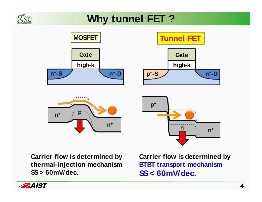
For Vdd ScalingWhy tunnel FET ?
log(
I d)
log(
I d)MOSFET Tunnel FET
Ioff 60 V/d
VV
off
VgVddV
Vg
60mV/dec
VddVddVddVdd
Conventionally Vdd scaling causes a significant increase in Ioff due to the lower limit of SS (~60mV/dec.)V li ith t I i b d b t i th SS
3
Vdd scaling without Ioff increase can be done by steepening the SS
MOSFET Tunnel FET
Why tunnel FET ?
MOSFET
hi h k
Gate
Tunnel FET
hi h k
Gate
high-kn+-S n+-D
high-kp+-S n+-D
n+ pp+
n+ p
n+n n+
Carrier flow is determined by thermal-injection mechanism
Carrier flow is determined by BTBT transport mechanism
4
thermal-injection mechanismSS > 60mV/dec.
BTBT transport mechanismSS < 60mV/dec.

Lateral & vertical TFETs• Two TFET architectures
Lateral (conventional) TFET Vertical(parallel electric field) TFET
Two TFET architectures
Gatehigh-k
Gate
(p )
high-k
S D S DXBOX BOX
L : Overlap length
X
LOV: Overlap length
BTBT is limited in interface-->> Small ID
BTBT area is enlargedC H t l VLSI TSA 2008 14 (2008)>> Small ID
5
C. Hu et.al., VLSI-TSA 2008, 14 (2008)R. Li et.al., Phys. Status Solidi C 9, 389 (2012)Y. Morita et.al, Jpn. J. Appl. Phys. 52, 04CC25 (2013)

Objective of this work
Performance of the parallel electric field TFET (PE TFET) relation between ON current and (PE-TFET), relation between ON current and overlap length, is analyzed.
Proposal of modified TFET architecture to improve l t t ti (S th ti l t i fi ld TFET)electrostatics (Synthetic electric field TFET)
6

Performance of the PE-TFET
7

S/D first & "Junction‐last" TFET process
Fabrication of PE-TFET with epichannel
SOI mesa etching (a)P I/I (b)BF2 I/I (c)
Si epitaxial growth, high-k and gate (d) Gate stack etch (e)Contact
50( ) (b) 5
Activation (1000 ˚C) Sintering
(d)SOI mesa etching
(a)
50 nm
TiNHigh-k
(a) (b)
TiN
5 nm
EpichannelP ion implantation(b)
(d)SOI SOIBOX
EpichannelHigh-kGate
High-kGate
SOIS D
TiN High-kMask Mask
P ion implantation
(e)
SOI SOI
BOX
BOX
SOI
BOX SOIBF2 ion implantation G G
Mask
(c)
(e)n-TFET p-TFET
High-k
8
S SD DBOX BOX

Operation of p- & n-PE-TFETs
ID-VG
TFET TFETG G
n-TFET p-TFET
High-k
S SD DBOX
9

Effect of LOV increaseRelation between ID and LOV
1.2(a) 101(b)
Relation between ID and LOVG
S D
0.8
/µm
) 10-1
/µm
)
S D
LOV
0.4I D (µ
A/
ID increase 10-3I D (µ
A/
00 40 80
10-5
100 101 102 103 1040 0 80LOV (nm) LOV (nm)
Confirming ID increase with increasing LOVConfirming ID increase with increasing LOVON current degraded at LOV > 1000 nm
10

Effect of LOV increaseAnalysis using a distributed-element circuit
( )
Gate insulatorThin channelID flow (voltage drop)
( d )Gate
y g
(x)VD
GiG C GC Ci
RC RC(x + dx)Gate
Thin channelGate insulator
xSource well
x = 0
L
x + dx RSRS
Source well
LOVSource input point
dv(x)dv(x)dx- = Rci(x)
di(x)dx- = Gv(x)
In ideal case (RS ~ 0),i-v relation can be describes as,
dx ( )
11

Effect of LOV increaseRelation between ID and LOV
2 RC
G VD
~GRC
1 =
(a)
101R
C
G VD~Ideal case(RS = 0)
(b)G
S D
Relation between ID and LOV
1.2
1.6
A/µm
)
CGRC
Ideal case10-1
A/µm
)
C SS D
LOV
0 4
0.8
1.2
I D (µ
A Ideal case(RS = 0)
Considering RS10-3I D
(µA
Considering RS
0
0.4
0 40 80 120L ( )
C s g S
10-5
100 101 102 103 104
LOV (nm) LOV (nm)
Upper limit of ON current ! G V
12
Upper limit of ON current !RC
VD~

Experimental results
Limit of drain current in PE-TFET
I G VIONMAX ~ GRC
VD
-->> Self-voltage-drop effect in thin channel
Trade offEnhancing G <<-->> Reducing RCEnhancing G << >> Reducing RC
Balance between tunnel conductance and h l i t i iti l
13
channel resistance is critical.

Proposal of modified TFET architecture
14

Proposal of synthetic electric field TFET
• Multiplication of lateral & vertical electric fields
Lateral TFET Synthetic electric field TFET(a)
Ultrathin undoped channel
(c)
Gate
(d)
Gate
High-kBOX
Gate
n+ S p+ D
EGATE
IT
undoped channel
Parallel electric field TFET
Gate
n+ SE
ESideIT
ESynth
WCH DEPIDEPI(b)
G t
n+ S p+ DBOX
ITBOX
ETop
WCHLOVBOX
Gate
p+ Dn+ SEGATE
IT
Slide 1515

Fabrication of SE-TFET with epichannel
• Based on source/drain-first CMOS process
(b) (c) (d)(a)As ion implantation
MaskMask MaskBF2 ion implantation
(b) (c) (d)
SOI
(a)
SOI
Channel epitaxial growth
SOIBOX
SOIBOX BOX BOX
Gate insulator(f) G t t h( )p-TFET n-TFET
Mesa-etching(e)Gate insulator& Gate electrode
(f) Gate etch(g)
BOX BOX BOXDSDS
Slide 16
BOX BOX BOX
16

Device structures
• Small amount of defects at epitaxial channel/source interface
Epitaxial h l
Gate electrode (TiN)
Channel cross-section
Gate cross section
50 nmn+ Source
channel Gate cross-section
Gate (TiN)HfO2
Gate insulator(HfO2)
( )
Source
50 nm
Slide 1717

Operation mechanism
Conventional (lateral) TFETSE-TFET
BOX p+ SEC
IT
ITI
n+ D
BTBT window
IT
Top E-field Side + Top E-fieldsBOX
Gate
n+ S p+ DEGATE
IT
Slide 18
Top E field Side + Top E fields
18

Simulation of electric field
• Electric field at edges is enlarged by SE-effect.• Scaling of channel thickness and width enhances
SE-effect
Electric field (V/cm)
Electric field distribution
3x10⁶
9x10⁵
lect c eld (V c )
EC
9x10⁴
3x10⁵
Electric field
1x10⁴
3x10⁴n+ Senhancement
W 20 D 10
Slide 19
WCH = 20 nm DEPI = 10 nm
19

Impact of channel width
• Better performance in narrower channel device
102ID-VG
100
10VD = -0.05 VWCH
0.17 um1
LOV = 400 nm100
de)
DEPI = 10 nm VD = -0.05 VLOV = 400 nm
4
10-2
uA/u
m)
= 52
1 um10 um
80
mV/
deca
d10-6
10-4
I D (u
SSMI
N =60
SSMI
N (m
10-8
10
-2.0 -1.0 0.0
DEPI = 10 nm 40102 103 104
Slide 20
VG (V) WCH (nm)
20

Impact of channel width
• ID at WCH = 0 corresponds to the edge current.
L 400 V = 1 V
2 0
2.5LOV = 400 nm VD = -1 V
VG = -2 V
1.5
2.0
I D (uA)
DEPI = 10 nm
0.1 uA/um
0.5
1.0DEPI = 16 nm0.7 uA
0.0 0 5 10 15 20W (um) 5 4 10 3 A/
0.2 uA
Slide 21
WCH (um) 5.4 x 10⁻³ uA/um
21
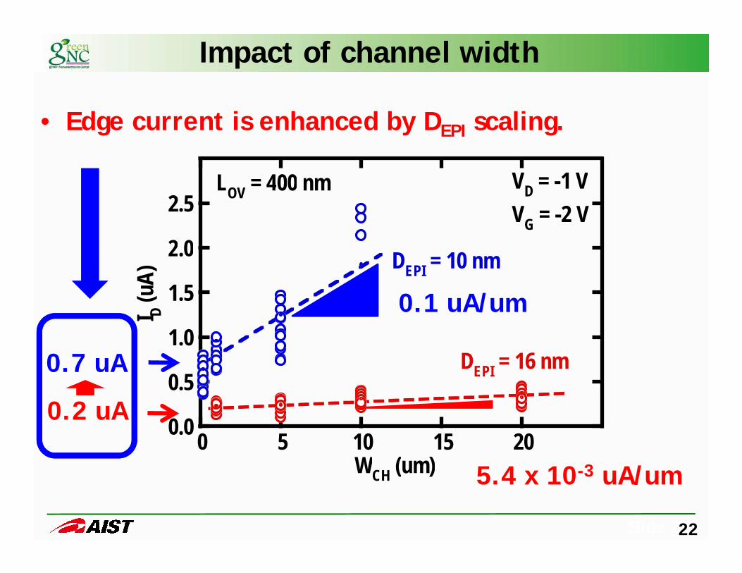
Impact of channel width
• Edge current is enhanced by DEPI scaling.
L 400 V = 1 V
2 0
2.5LOV = 400 nm VD = -1 V
VG = -2 V
1.5
2.0
I D (uA)
DEPI = 10 nm
0.1 uA/um
0.5
1.0DEPI = 16 nm0.7 uA
0.0 0 5 10 15 20W (um) 5 4 10 3 A/
0.2 uA
Slide 22
WCH (um) 5.4 x 10⁻³ uA/um
22

Impact of channel width
• Scaling of both DEPI and WCH enhance performance
102
100
102
)
4 nm(Prediction)
DEPI = 16 nm
10-2
100
(uA/
um)
10 nmDEPI = 16 nm
GateG t
FinFET-like structure is better
10-4
10 2
I D
EC
Gate
S
EC
Gate
S10 4
100 101 102 103 104 105
n+ Sn+ S
Slide 23
WCH (nm)
23

ID‐VG ID‐VD
Performance of SE-tunnel FinFET
1
103 VD = -0.2, -1.0 V
6070 -1.0 V V
G 0.1 V step
10-1
101
A/um
) LG
60 nm=405060
A/um
) -0.9 V
10-3I D (uA L
OV
WFIN
D
10 nm
12 nm7 nm
=
==
2030I D (u
A
-0.8 V
-0.7 V
10-7
10-5
2 1 0
DSOI
DEPI
SSMIN
= 58
7 nm25 nm
==
010
0 8 0 4 0 0
-0.6 V-0.5 V-0.4 V
-2 -1 0V
G (V)
-0.8 -0.4 0.0V
D (V)
Significant performanceSS 58 I 4 uA/um @(V V ) ( 0 5 0 2 V)
24
SSMIN = 58, ID = 4 uA/um @(VG,VD)=(-0.5,-0.2 V)400 uA/um @(VG,VD)=(-2,-1 V)

Summary
Parallel electric field TFET• Limit of ON current• Balance between tunnel conductance and channel Balance between tunnel conductance and channel
resistance is critical
S th ti l t i fi ld TFETSynthetic electric field TFET• Scaling induced performance enhancement• FinFET-like slim device is promising.p g.• Significant performance in small voltage
SSMIN = 58, ID = 4 uA/um @(VG,VD)=(-0.5,-0.2 V)400 A/ @(V V ) ( 2 1 V)400 uA/um @(VG,VD)=(-2,-1 V)
• The concept can be applicable to Ge or III-V TFETs.
25
The concept can be applicable to Ge or III V TFETs.

Acknowledgement
This research was supported by JSPS through the First Program, “Development of Core Technologies
for Green Nanoelectronics”.
Thank you for your kind attention.
Slide 2626

2
Benchmark
101
102um
)[1] G. Zhou, et al., IEDM 2012[2] A. Villalon, et al., VLSI2012[3] G. Dewey, et al., IEDM 2011
[1]
[2][4]
100
10
curre
nt (u
A/u [4] W. Choi,et al., EDL28 2007
[5] K. Tomioka, et al., VLSI2012
[2][3] (0.3V)
[5]
10-1
ON c
Red: Si, SiGe
10-2
0 60 120 180SS (mV/dec)
Blue: III-V
SS (mV/dec)
Our data(No strain, no Ge, no metal SD, only by device consideration)

Impact of LOV
WCH = 10 um
• Maximum ID at LOV ~ 50 nm
0 15
0.20
)CH
0.10
0.15
D (uA/
um
DEPI = 10 nm
0.05
I D
DEPI = 16 nm
0.001 10 100 1000
Slide 28
LOV (nm)

Scaling of channel width
SE-tunnel FinTFET
• Scaling of both DEPI and WFIN enhance performance.
p+ Source
BTBT IT
BTBT window
Slide 29
Both Sides + Top E-fields
29

1 E+04
1,E+03
1,E+04WFIN-scaling-induced ID
increase
1,E+02
um)
1,E+01
I D(u
A/u
DEPI = 7 nm
1,E-01
1,E+00
DEPI = 16 nm 10 nm
DEPI 7 nm
,1,E+00 1,E+01 1,E+02 1,E+03 1,E+04 1,E+05
WFIN (nm)
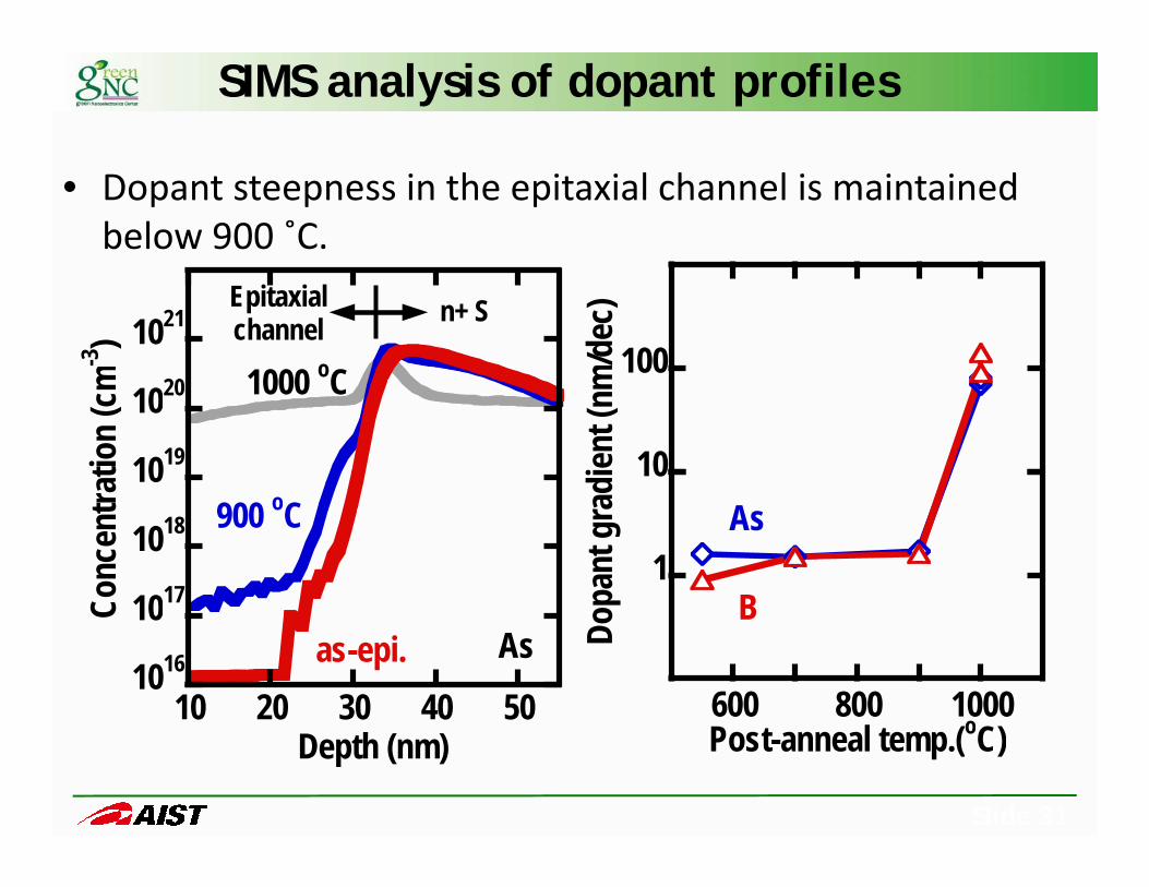
SIMS analysis of dopant profiles
• Dopant steepness in the epitaxial channel is maintained below 900 ˚C.
1020
1021
m-3
)
1000 oC
Epitaxialchannel n+ S
100m/d
ec)
1019
1020
ratio
n (c
m
o
1000 C
10
adien
t (nm
1017
1018
Conc
entr 900 oC
1op
ant g
raB
As
1016
10
10 20 30 40 50
C
as-epi. As600 800 1000
Do
o
B
Slide 31
Depth (nm) Post-anneal temp.(oC)

Impact of SE effect
• Significant increase of ID in the SE-TFET
GateID-VG
100
With SE effect
WCH
= 10 um DEPI
= 10 nmGate
BOXn+ S
E`C
10-4
10-2
uA/u
m) BOX
SE-TFET
10-6
10
I D (u
GateEC
10-8-2.0 -1.0 0.0
V (V)
Without SE effectBOXn+ S
EC
Slide 32
VG (V)Parallel electric field TFET

This work This work This work This workVillalon et alVLSI2012
[8]
Villalon et alVLSI2012
[8]
Knoll et alEDL2013
[9]
Zhou et alIEDM2012
[10]
Zhou et alIEDM2012
[10]
Dewey et alIEDM2011
[11]Types p p p p p p p n n nTypes p p p p p p p n n n
Materials Si Si Si Si SiGe30% SiGe30% Si GaSb/InAs GaSb/InAs InGaAsStructures DL Fin DL Fin DL Fin DL Fin ETSOI ETSOI Nanowire Vertical Vertical Vertical
Boosters DL Fin DL Fin DL Fin DL Fin Strain Strain StrainM t l S/D III-V III-V III-VMetal S/D
VD (V) -1 -1 -0.2 -0.2 -1 -1 -0.5 1 0.5 0.3VG (V) -2 -1 -1 -0.5 -2 -1 -1 1 0.5 ~0.48
VON-VOFF(V) -2 -1 -1 -0.5 -2 -1 -1 2 1.5 0.5(V) 0 5 5 0 5
ION (uA/um) 417 82 40 4 ~300 ~10 ~5 380 180 5.7IMIN (uA/um) 2.00E-04 2.00E-04 2.00E-06 2.00E-06 3.70E-05 3.70E-05 ~2e-6 5.07E-02 3.00E-02 1.00E-04
ION/IMIN 2.09E+06 4.10E+05 2.00E+07 2.00E+06 8.11E+06 2.70E+05 2.50E+06 7.50E+03 6.00E+03 5.70E+04SSMIN
(mV/dec) 70 70 58 58 ~120 ~120 90 200 200 58
EOT (nm) 1.3 1.3 1.3 1.3 1.25 1.25 3 nm HfO2 1.3 1.3 1.1LG (nm) 60 60 60 60 200 200 200 - - 100

ID-VG of SE-TFETs
• Symmetric operation of p & n SE‐TFETs
102 LG = 100 nm WCH = 60 nm
100D
EPI = 9 nm
10-4
10-2
(uA/
um)
SSMIN
= 70SS = 69
10-6
10 4
I D (
VD = -0.2, V
D = 0.2,
MINSSMIN
69
10-8-2.0 -1.0 0.0 1.0 2.0
V (V)
-1 V 1 V
Slide 34
VG (V)

p‐TFETLg = 1 um
Tunability of LOV
Lg = 1 umLw = 10 um
35
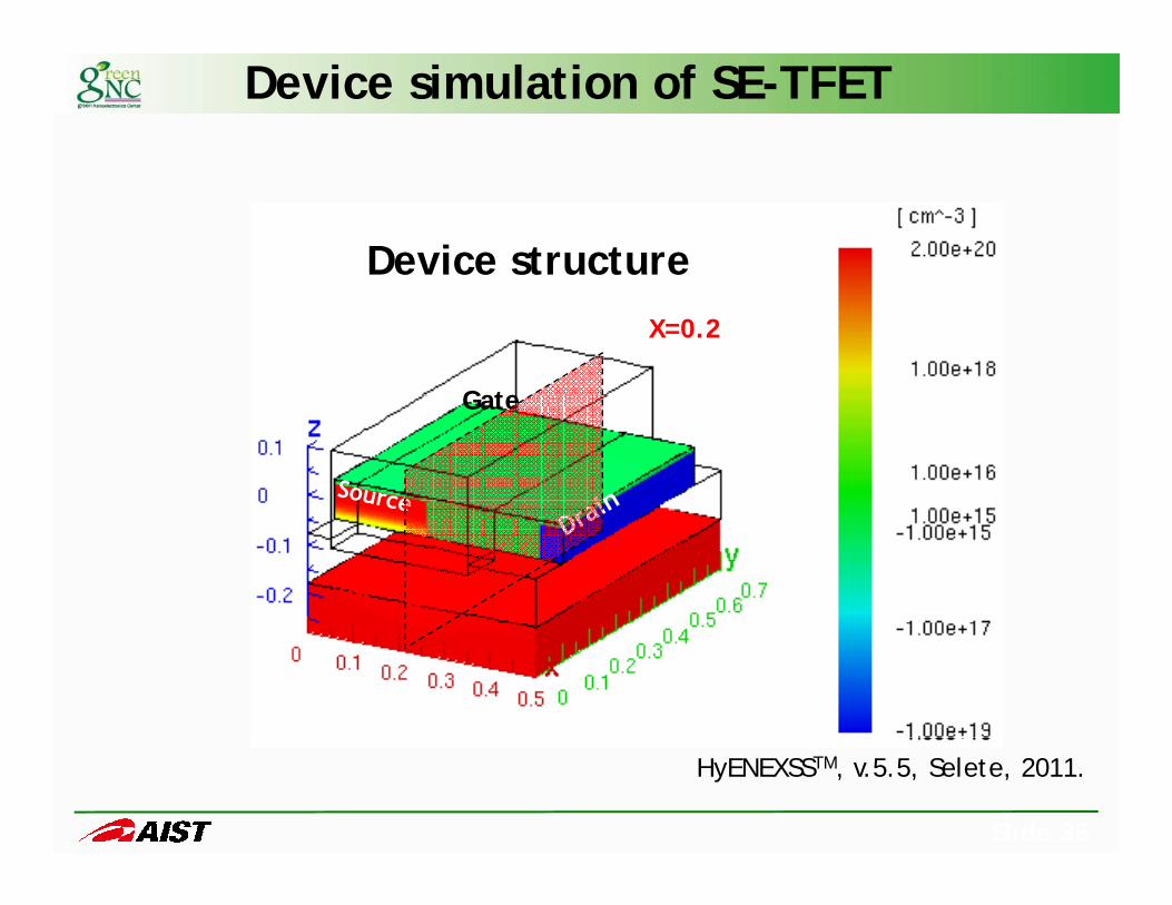
Device simulation of SE-TFET
Device structure
Gate
X=0.2
Gate
Slide 36
HyENEXSSTM, v.5.5, Selete, 2011.

Sub‐threshold condition (Potential) X=0.2
source
sourceBOX
Saturation condition (Potential)
source
sourceBOX
Slide 37
sourceBOX

Sub‐threshold condition (Potential) X=0.2
source
sourceBOX
Saturation condition (Potential)
Potential difference > Si band gap
BTBT i d t dsource
sourceBOX
BTBT window opens at edge.
Slide 38
sourceBOX


![Introduction to Probability Models · 2017. 6. 23. · Answers and Solutions 5 = 1 ·P(E) + 0 ·P(F) + P{E before F} = [1 −P(E) −P(F)] Therefore, P{E before F} = P(E) P(E) + P(F)](https://static.fdocuments.in/doc/165x107/6112ee880abfa96f265eed56/introduction-to-probability-models-2017-6-23-answers-and-solutions-5-1-pe.jpg)