P. Denes 02.02 Page 1 FPPA-Clock Clocks FPPA From CTRL To all FPPA ADC Clocks are received by CTRL...
20
P. Denes 02.02 Page 1 FPPA-Clock Clock s FPPA From CTRL To all FPPA ADC Clocks are received by CTRL chip and distributed as PECL signals to the FPPAs (in parallel) Each FPPA re-generates the clock for the ADC (this because the ADC clock is at a non-standard voltage and to save power.
-
Upload
miles-griffin -
Category
Documents
-
view
213 -
download
0
Transcript of P. Denes 02.02 Page 1 FPPA-Clock Clocks FPPA From CTRL To all FPPA ADC Clocks are received by CTRL...

P. Denes 02.02
Page 1FPPA-Clock
Clocks
Clocks
FPPA
From CTRLTo all FPPA
ADC
• Clocks are received by CTRL chip and distributed as PECL signals to the FPPAs (in parallel)• Each FPPA re-generates the clock for the ADC (this is because the ADC clock is at a non-standard voltage, and to save power.
P. Denes 02.02
Page 2FPPA-Clock
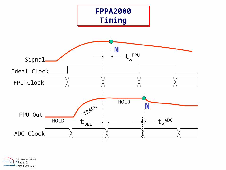
FPPA2000 Timing
FPPA2000 Timing
Signal
Ideal Clock
FPU Clock
FPU Out TRACKHOLD
ADC Clock
NtA
FPU
tDEL
N
HOLD tAADC
P. Denes 02.02
Page 3FPPA-Clock
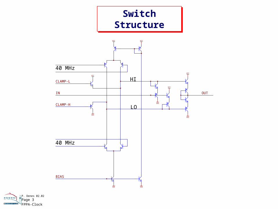
Switch StructureSwitch
StructureVCC VCC
IN
VEE
VCC
OUT
VEE
VCC
VEE VEE
VEE
VCC
BIAS
CLAMP-H
CLAMP-L
40 MHz
40 MHz
HI
LO

P. Denes 02.02
Page 4FPPA-Clock
Schematic Level
Schematic Level
0
0.5
1
1.5
2
2.5
3
3.5
4
4.5
000.0E+0 50.0E-9 100.0E-9 150.0E-9 200.0E-9Time [s]
Am
plitu
de [
V] in
clklohiout

P. Denes 02.02
Page 5FPPA-Clock
In Detail
In Detail
0
0.5
1
1.5
2
2.5
3
3.5
4
4.5
70.0E-9 95.0E-9 120.0E-9
Time [s]
Am
plitu
de [
V]
VCC VCC
IN
VEE
VCC
OUT
VEE
VCC
VEE VEE
VEE
VCC
BIAS
CLAMP-H
CLAMP-L
Response dependson this slew rate

P. Denes 02.02
Page 6FPPA-Clock
Post-Layout FPU Simulation
Post-Layout FPU Simulation
-0.3
-0.1
0.1
0.3
0.5
0.7
0.9
1.1
1.3
1.5
20 45 70 95 120 145 170 195 220 245 270 295
Time [ns]
FPU-PedADC Clock
1+ TeV signal
x33
x5
x1
x5 x9

P. Denes 02.02
Page 7FPPA-Clock
-0.3
-0.1
0.1
0.3
0.5
0.7
0.9
1.1
1.3
1.5
75 100 125 150 175
Time [ns]
FPU-PedADC ClockPreamp
Sampling
Sampling
H S
Sle
w 3
3
H S H S
“scaled by eye”
Decide: Change Range
HSRecovery

P. Denes 02.02
Page 8FPPA-Clock
Overall Chain - Settling and Propagation Time
Overall Chain - Settling and Propagation Time
T/H BUF MUX OutBUF
Clocks Clocks

P. Denes 02.02
Page 9FPPA-Clock
Schematic-Level Timing
Schematic-Level Timing
MU
Xou
t
FP
Uou
t
CK
AD >5 ns between
FPUout and CKAD
P. Denes 02.02
Page 10FPPA-Clock
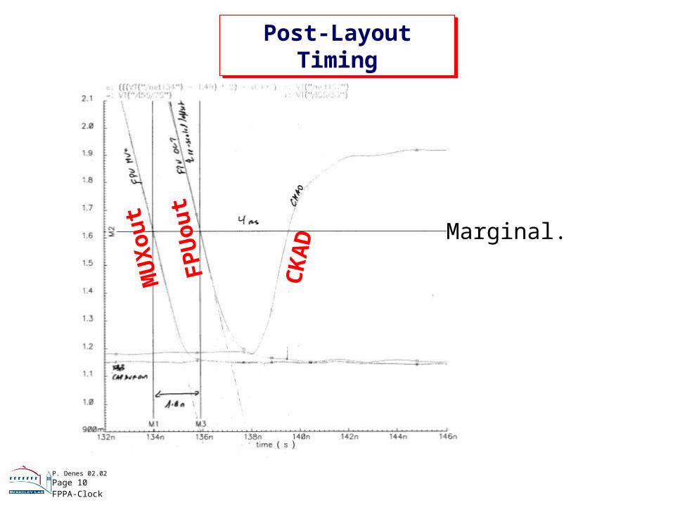
Post-Layout Timing
Post-Layout Timing
MU
Xout
FP
Uout
CK
AD Marginal.
P. Denes 02.02
Page 11FPPA-Clock
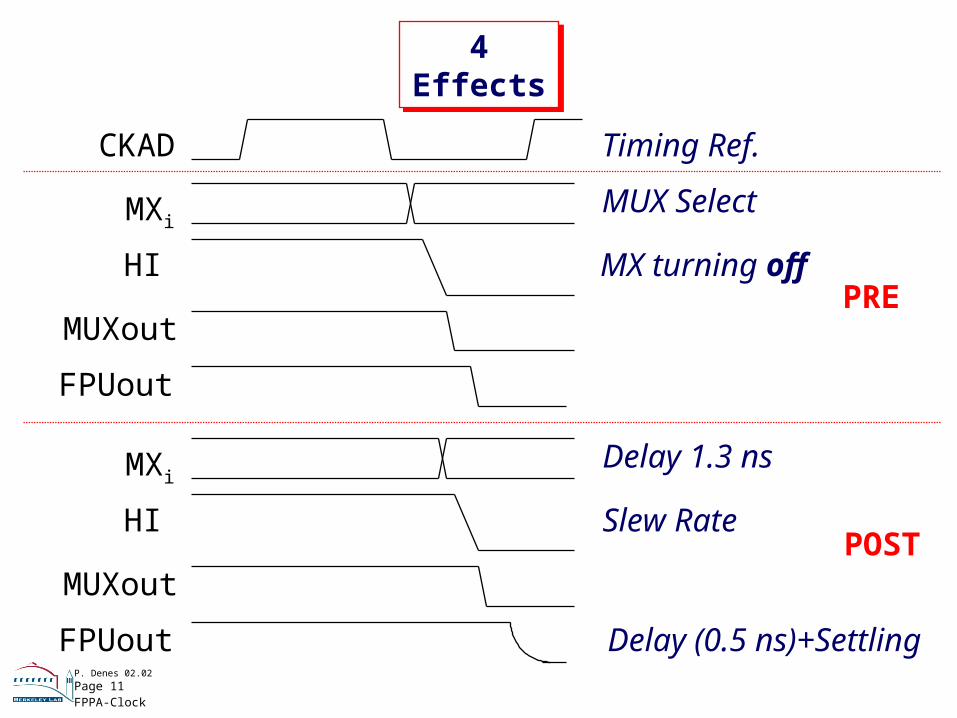
4 Effects
4 Effects
CKAD Timing Ref.
MXiMUX Select
HI
MUXout
MX turning off
FPUout
MXi
HI
MUXout
FPUout
PRE
POST
Delay 1.3 ns
Slew Rate
Delay (0.5 ns)+Settling

P. Denes 02.02
Page 12FPPA-Clock
FPU Data Bits
FPU Data Bits
0
0.5
1
1.5
2
2.5
3
3.5
4
4.5
5
175 180 185 190 195 200
Time [ns]
FPU
0 a
nd 1
1
1.1
1.2
1.3
1.4
1.5
1.6
1.7
1.8
1.9
2
CK
AD
_fpo0_1n_fpo1_1n_ckad100p
Note ~6 ns delaybetween CKADand FPU0…
P. Denes 02.02
Page 13FPPA-Clock
End of FPPA2000 Part

P. Denes 02.02
Page 14FPPA-Clock
FPPA2000/1 Timing
FPPA2000/1 Timing
CK In
CK ADC
CK S/H
CK In
CK ADC
CK S/HDelay(Fixed)
Delay(Var.)
FPPA2000
FPPA2001
Add delay to allow clock adjustment
P. Denes 02.02
Page 15FPPA-Clock
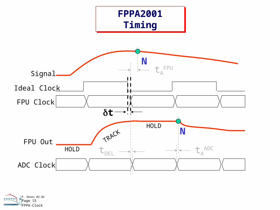
FPPA2001 Timing
FPPA2001 Timing
Signal
Ideal Clock
FPU Clock
FPU Out TRACKHOLD
ADC Clock
NtA
FPU
tDEL
N
HOLD tAADC
t
P. Denes 02.02
Page 16FPPA-Clock
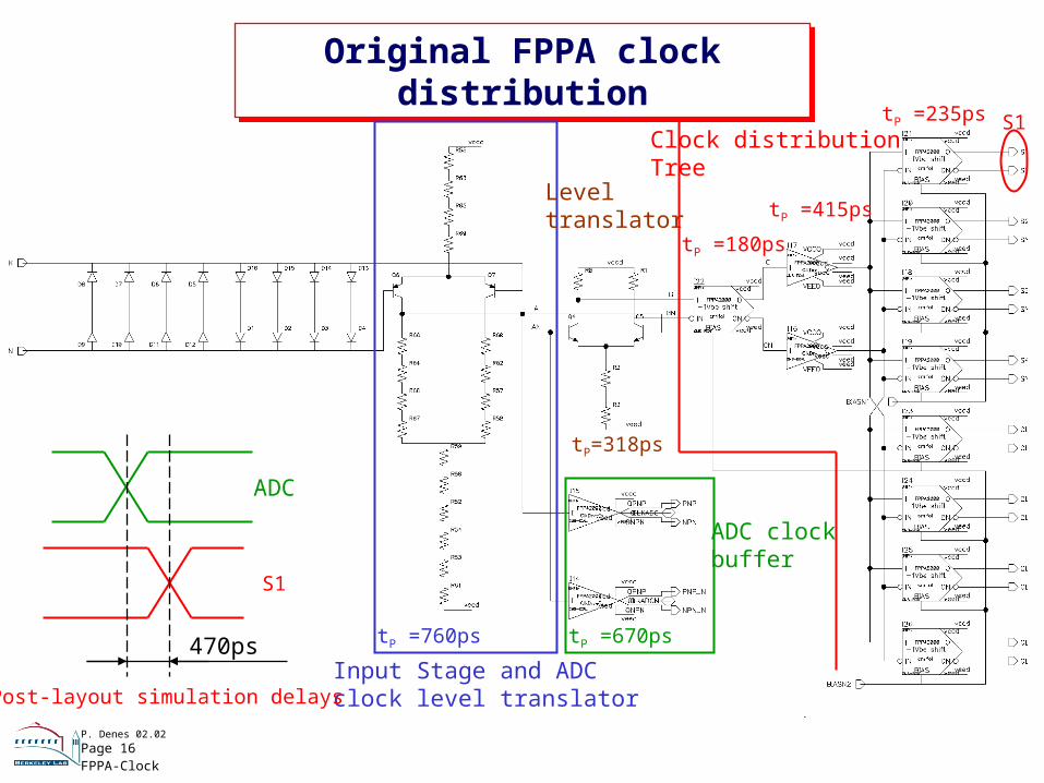
Original FPPA clock distribution
Original FPPA clock distribution
Input Stage and ADC clock level translator
ADC clockbuffer
Leveltranslator
Clock distributionTree
tP =760ps tP =670ps
tP =180ps
tP =415ps
tP =235ps
tP=318ps
ADC
S1
470ps
S1
Post-layout simulation delays

P. Denes 02.02
Page 17FPPA-Clock
New Clock DistributionNew Clock
Distribution
Internal Clock Delay
ADC Clock buffer
ADC Clock Delay
Clock distribution Tree
Leveladapter
Clock Input
393ps 111ps 126ps285ps
511ps
126ps6.2ns
111ps
297ps111ps
t
S1 to Clock ADC delay adjustableFrom -1ns to 6ns
P. Denes 02.02
Page 18FPPA-Clock
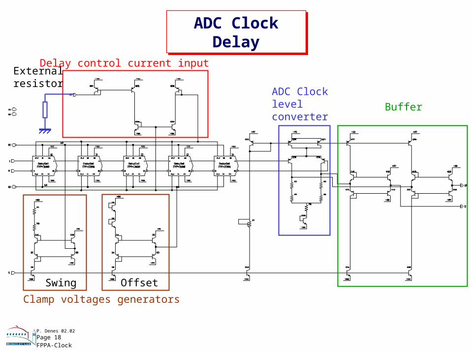
ADC Clock Delay
ADC Clock Delay
ADC Clock level converter
Buffer
Delay control current inputExternalresistor
Clamp voltages generators
Swing Offset

P. Denes 02.02
Page 19FPPA-Clock
Delay Cell
Delay Cell
Current switch Clamp circuit
250f 250f
P. Denes 02.02
Page 20FPPA-Clock
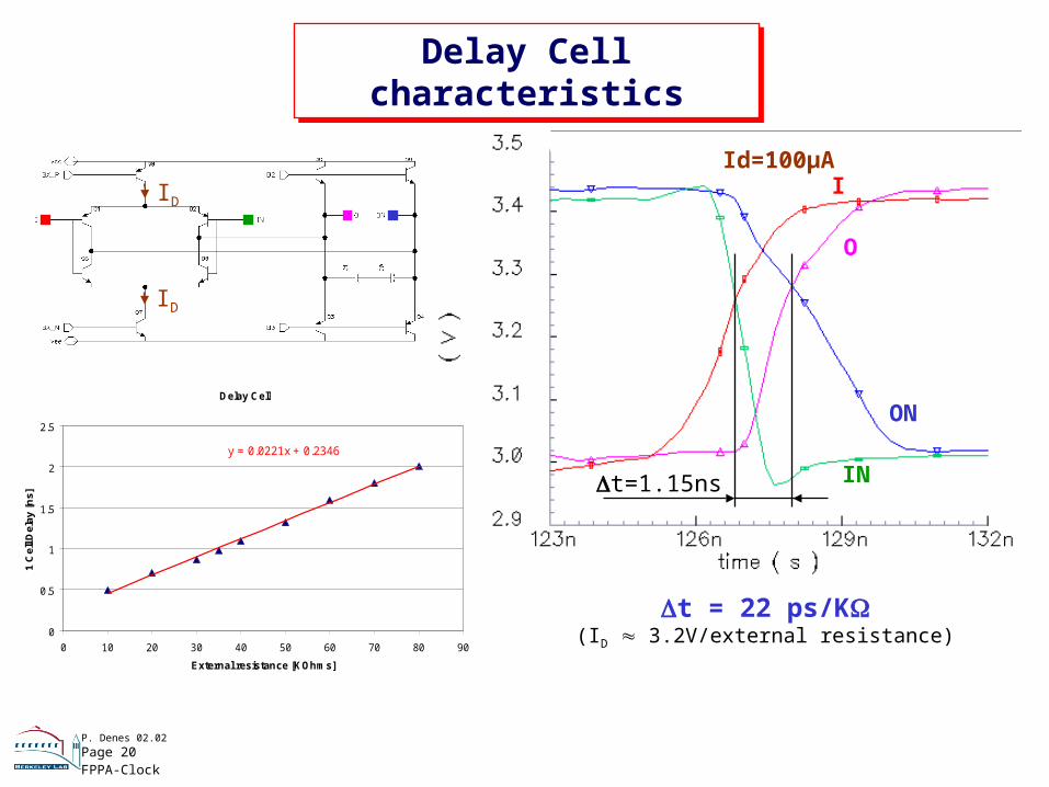
Delay Cell characteristics
Delay Cell characteristics
ID
ID
IN
I
ON
O
t=1.15ns
Id=100μA
Delay Cell
y = 0.0221x + 0.2346
0
0.5
1
1.5
2
2.5
0 10 20 30 40 50 60 70 80 90
External resistance [KOhms]
1 C
ell
De
lay
[n
s]
t = 22 ps/K(ID 3.2V/external resistance)