Overview on the development of front-end building blocks
42
Overview on the Overview on the development of front-end development of front-end building blocks building blocks Eduard Atkin (MEPhI), Eduard Atkin (MEPhI), Alexander Voronin (MSU) Alexander Voronin (MSU) Workshop on Silicon Detector Systems for the CBM experiment at Workshop on Silicon Detector Systems for the CBM experiment at FAIR, April 18-20, 2007 FAIR, April 18-20, 2007
-
Upload
latifah-warren -
Category
Documents
-
view
23 -
download
2
description
Overview on the development of front-end building blocks. Eduard Atkin ( MEPhI ), Alexander Voronin (MSU). Workshop on Silicon Detector Systems for the CBM experiment at FAIR, April 18-20, 2007. Outline. PART I – Design aspects Specifications Chip structure and building block list - PowerPoint PPT Presentation
Transcript of Overview on the development of front-end building blocks
Overview on the Overview on the development of front-development of front-
end building blocksend building blocks
Eduard Atkin (MEPhI), Eduard Atkin (MEPhI),
Alexander Voronin (MSU)Alexander Voronin (MSU)
Workshop on Silicon Detector Systems for the CBM experiment at FAIR, April 18-20, 2007Workshop on Silicon Detector Systems for the CBM experiment at FAIR, April 18-20, 2007
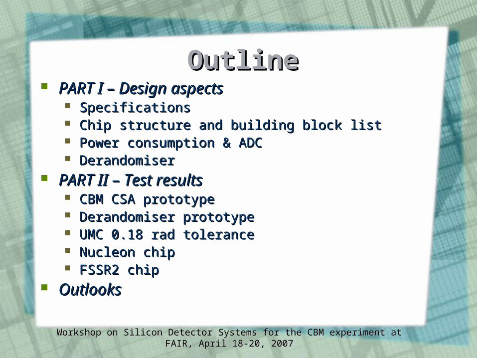
OutlineOutline PART I – Design aspectsPART I – Design aspects
SpecificationsSpecifications Chip structure and building block listChip structure and building block list Power consumption & ADCPower consumption & ADC DerandomiserDerandomiser
PART II – Test resultsPART II – Test results CBM CSA prototypeCBM CSA prototype Derandomiser prototypeDerandomiser prototype UMC 0.18 rad toleranceUMC 0.18 rad tolerance Nucleon chipNucleon chip FSSR2 chipFSSR2 chip
OutlooksOutlooks
Workshop on Silicon Detector Systems for the CBM experiment at FAIR, April 18-20, 2007Workshop on Silicon Detector Systems for the CBM experiment at FAIR, April 18-20, 2007
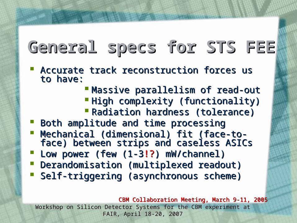
General specs for STS FEEGeneral specs for STS FEE Accurate track reconstruction forces us to Accurate track reconstruction forces us to
have:have: Massive parallelism of read-outMassive parallelism of read-out High complexity (functionality) High complexity (functionality) Radiation hardness (tolerance) Radiation hardness (tolerance)
Both amplitude and time processingBoth amplitude and time processing Mechanical (dimensional) fit (face-to-face) Mechanical (dimensional) fit (face-to-face)
between strips and caseless ASICsbetween strips and caseless ASICs Low power (few (Low power (few (11-3-3!?!?) mW/channel)) mW/channel) Derandomisation (multiplexed readout)Derandomisation (multiplexed readout) Self-triggering (asynchronous scheme)Self-triggering (asynchronous scheme)
Workshop on Silicon Detector Systems for the CBM experiment at FAIR, April 18-20, 2007Workshop on Silicon Detector Systems for the CBM experiment at FAIR, April 18-20, 2007
CBM Collaboration Meeting, March 9-11, 2005CBM Collaboration Meeting, March 9-11, 2005
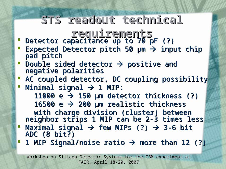
STS readout technical STS readout technical requirementsrequirements
Detector capacitance up to 70 pF (?)Detector capacitance up to 70 pF (?) Expected Detector pitch 50 Expected Detector pitch 50 µµm m input chip pad input chip pad
pitch pitch Double sided detector Double sided detector positive and negative positive and negative
polaritiespolarities AC coupled detector, DC coupling possibilityAC coupled detector, DC coupling possibility Minimal signal Minimal signal 1 MIP: 1 MIP: 11000 e 11000 e 150 150 µµm detector thickness (?) m detector thickness (?) 16500 e 16500 e 200 200 µµm realistic thicknessm realistic thickness with charge division (cluster) between neighbor with charge division (cluster) between neighbor
strips 1 MIP can be 2-3 times less strips 1 MIP can be 2-3 times less Maximal signal Maximal signal few MIPs (?) few MIPs (?) 3-6 bit ADC (8 3-6 bit ADC (8
bit?)bit?) 1 MIP Signal/noise ratio 1 MIP Signal/noise ratio more than 12 (?) more than 12 (?)
Workshop on Silicon Detector Systems for the CBM experiment at FAIR, April 18-20, 2007Workshop on Silicon Detector Systems for the CBM experiment at FAIR, April 18-20, 2007

STS readout technical STS readout technical requirements requirements
IIII 100 ns double hit resolution100 ns double hit resolution Time stamp resolution 2-4 ns (?)Time stamp resolution 2-4 ns (?) Input current pulse duration 10 nsInput current pulse duration 10 ns Radiation hardness 1 Mrad (15?)Radiation hardness 1 Mrad (15?) 2-4 mW/channel2-4 mW/channel Temperature 0…50Temperature 0…50ooC (?)C (?) Dead-time free Dead-time free Self-triggeredSelf-triggered
Workshop on Silicon Detector Systems for the CBM experiment at FAIR, April 18-20, 2007Workshop on Silicon Detector Systems for the CBM experiment at FAIR, April 18-20, 2007
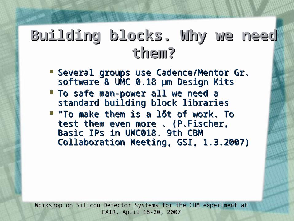
Building blocks. Why we need Building blocks. Why we need them?them?
Several groups use Cadence/Mentor Several groups use Cadence/Mentor Gr. software & UMC 0.18 Gr. software & UMC 0.18 µµm Design m Design KitsKits
To safe man-power all we need a To safe man-power all we need a standard building block librariesstandard building block libraries
““To make them is a lot of work. To To make them is a lot of work. To test them even more”. (P.Fischer, test them even more”. (P.Fischer, Basic IPs in UMC018. 9th CBM Basic IPs in UMC018. 9th CBM Collaboration Meeting, GSI, 1.3.2007)Collaboration Meeting, GSI, 1.3.2007)
Workshop on Silicon Detector Systems for the CBM experiment at FAIR, April 18-20, 2007Workshop on Silicon Detector Systems for the CBM experiment at FAIR, April 18-20, 2007
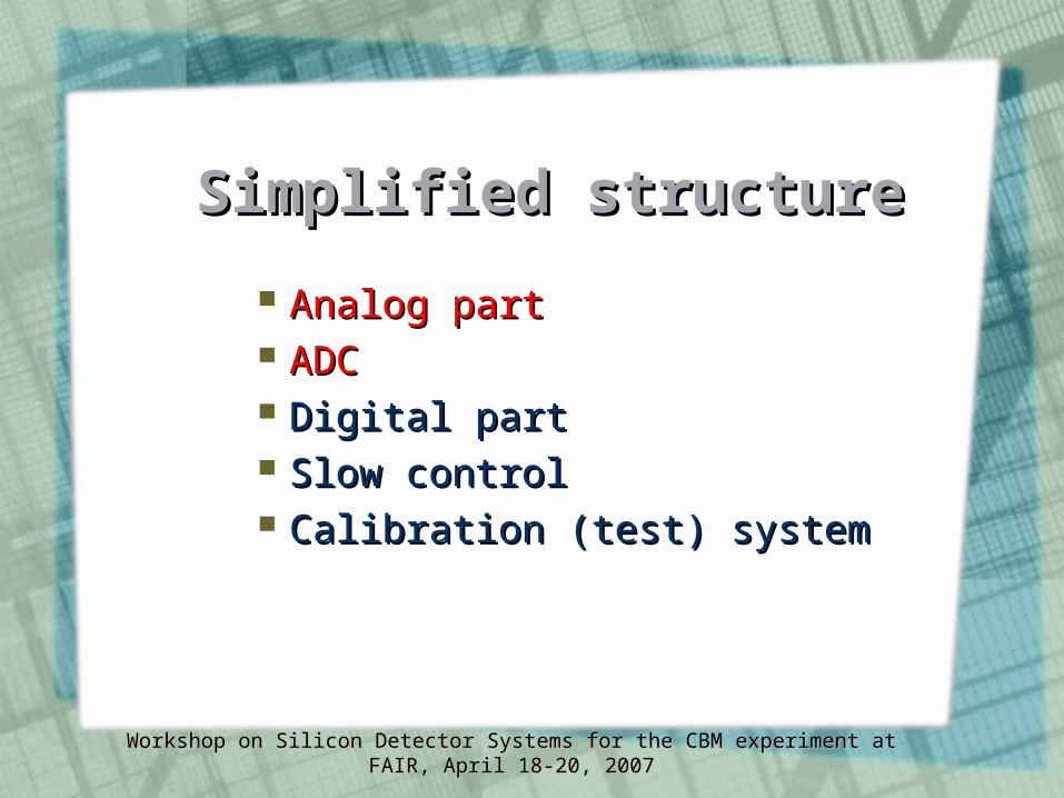
Simplified structureSimplified structure
Analog partAnalog part ADCADC Digital partDigital part Slow controlSlow control Calibration (test) systemCalibration (test) system
Workshop on Silicon Detector Systems for the CBM experiment at FAIR, April 18-20, 2007Workshop on Silicon Detector Systems for the CBM experiment at FAIR, April 18-20, 2007
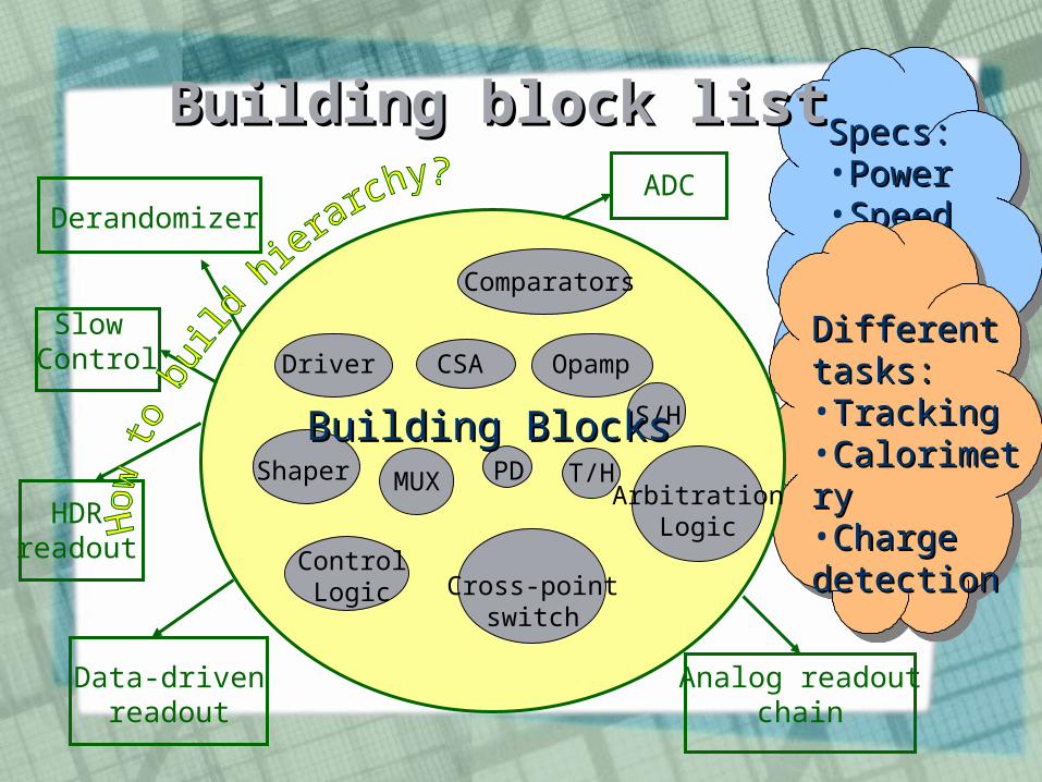
Specs:Specs:•PowerPower•SpeeSpeedd
Building block listBuilding block list
CSA Opamp
Comparators
PD T/H
S/H
Cross-pointswitch
Driver
ShaperArbitration
Logic
MUX
ControlLogic
Building BlocksBuilding Blocks
ADC
Analog readoutchain
Derandomizer
HDRreadout
Data-drivenreadout
Slow Control
Different Different tasks:tasks:•TrackingTracking•CalorimetrCalorimetryy•Charge Charge detectiondetection
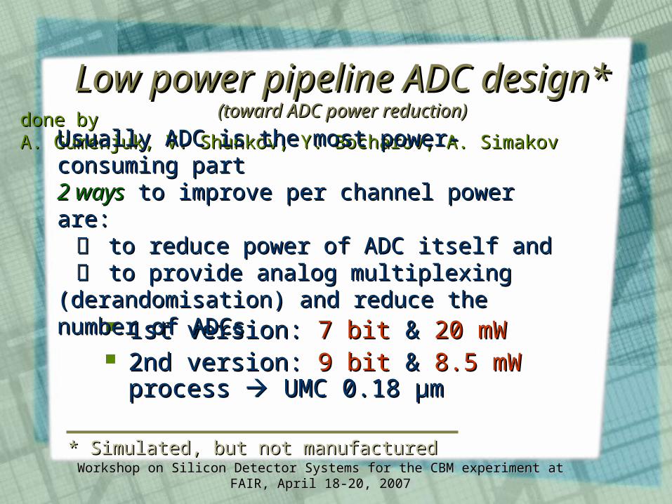
Low power pipeline ADC Low power pipeline ADC design*design*
((toward ADC power reductiontoward ADC power reduction))
1st version: 1st version: 7 bit7 bit && 20 mW20 mW 2nd version: 2nd version: 9 bit9 bit && 8.5 mW8.5 mW
process process UMC 0.18 UMC 0.18 µµmm
done bydone byA. Gumenjuk, V. Shunkov, Y. Bocharov, A. SimakovA. Gumenjuk, V. Shunkov, Y. Bocharov, A. Simakov
* Simulated, but not manufactured* Simulated, but not manufactured
Workshop on Silicon Detector Systems for the CBM experiment at FAIR, April 18-20, 2007Workshop on Silicon Detector Systems for the CBM experiment at FAIR, April 18-20, 2007
Usually ADC is the most power-consuming Usually ADC is the most power-consuming part part 2 ways2 ways to improve per channel power are: to improve per channel power are: ᅳᅳ to reduce power of ADC itself andto reduce power of ADC itself and ᅳᅳ to provide analog multiplexingto provide analog multiplexing (derandomisation) and reduce the number of (derandomisation) and reduce the number of ADCsADCs
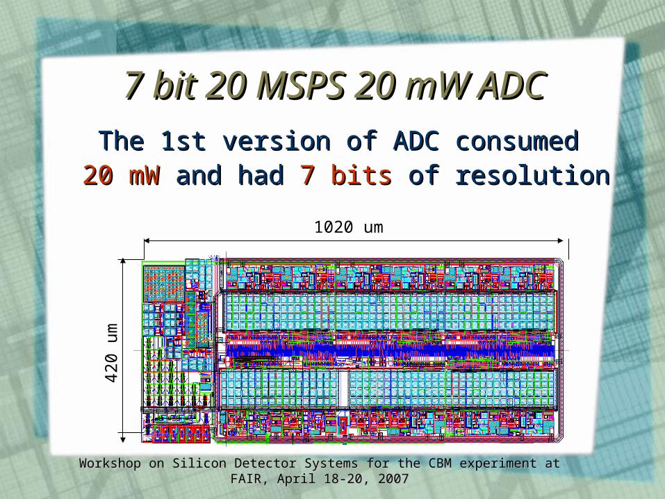
7 bit 20 MSPS 20 mW ADC7 bit 20 MSPS 20 mW ADCThe 1st version of ADC consumed The 1st version of ADC consumed 20 mW20 mW and had and had 7 bits7 bits of resolution of resolution
1020 um
420
um
Workshop on Silicon Detector Systems for the CBM experiment at FAIR, April 18-20, 2007Workshop on Silicon Detector Systems for the CBM experiment at FAIR, April 18-20, 2007
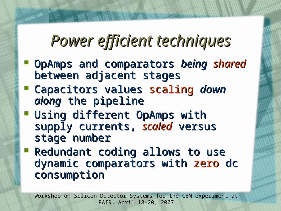
OpAmps and comparators OpAmps and comparators beingbeing sharedshared between adjacent stages between adjacent stages
Capacitors valuesCapacitors values scalingscaling downdown alongalong the pipelinethe pipeline
Using different OpAmps withUsing different OpAmps with supply supply currents, currents, scaledscaled versus stage number versus stage number
Redundant coding allows to useRedundant coding allows to use dynamic comparators withdynamic comparators with zerozero dc dc consumptionconsumption
Power efficient techniquesPower efficient techniques
Workshop on Silicon Detector Systems for the CBM experiment at FAIR, April 18-20, 2007Workshop on Silicon Detector Systems for the CBM experiment at FAIR, April 18-20, 2007
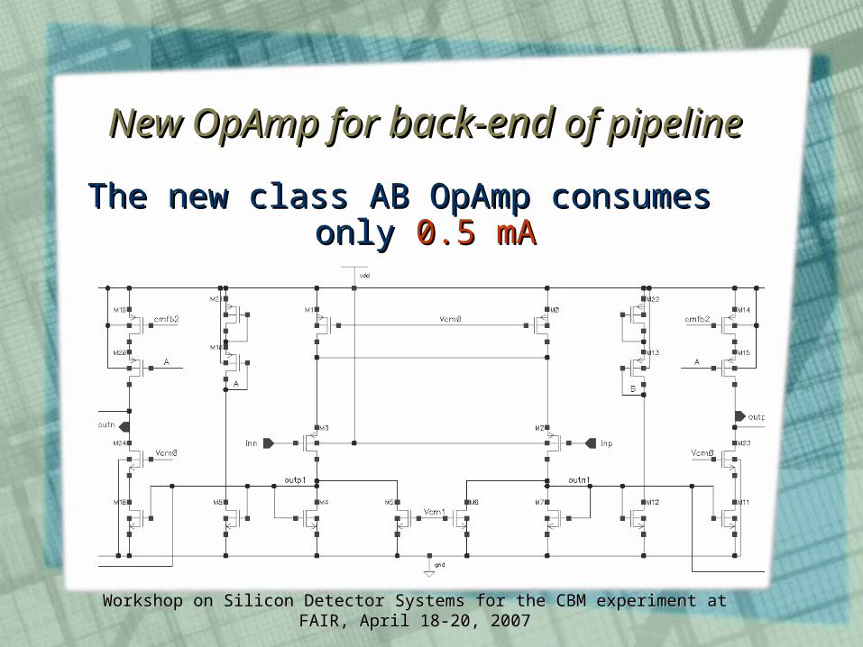
New OpAmp for New OpAmp for back-endback-end of of pipelinepipeline
The new class AB OpAmp consumesThe new class AB OpAmp consumes onlyonly 0.5 mA0.5 mA
Workshop on Silicon Detector Systems for the CBM experiment at FAIR, April 18-20, 2007Workshop on Silicon Detector Systems for the CBM experiment at FAIR, April 18-20, 2007
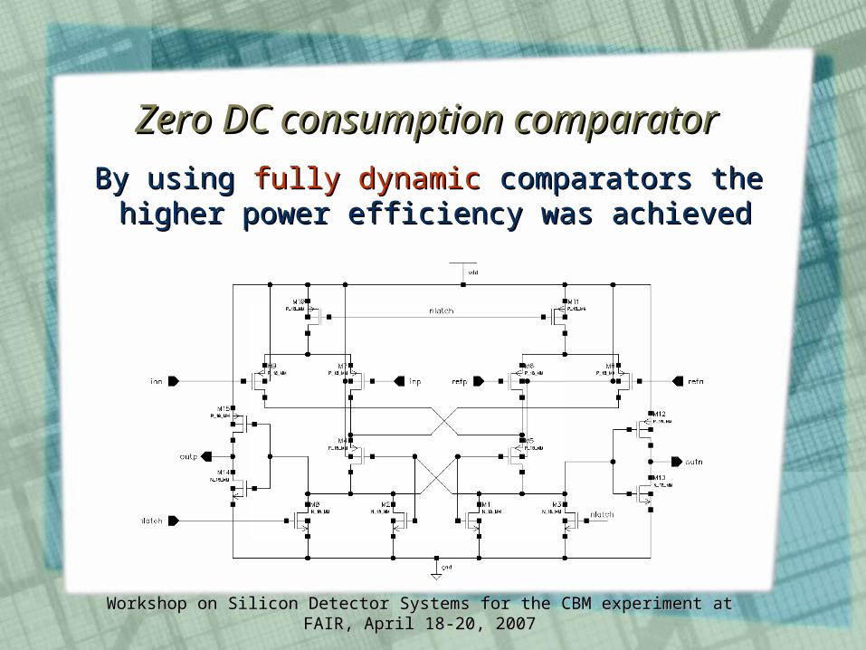
Zero DC consumption comparatorZero DC consumption comparator
By using By using fully dynamicfully dynamic comparators the comparators the higher power efficiency was achievedhigher power efficiency was achieved
Workshop on Silicon Detector Systems for the CBM experiment at FAIR, April 18-20, 2007Workshop on Silicon Detector Systems for the CBM experiment at FAIR, April 18-20, 2007
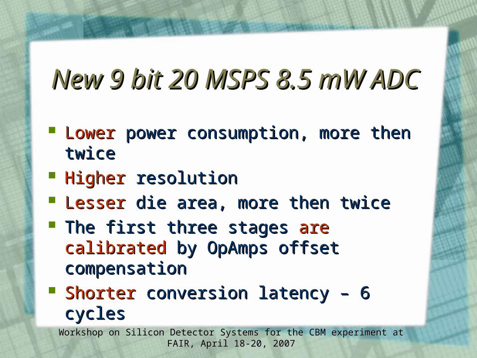
LowerLower power consumption, more then power consumption, more then twicetwice
HigherHigher resolution resolution LesserLesser die area, more then twice die area, more then twice The first three stages The first three stages are calibratedare calibrated
by OpAmps offset compensationby OpAmps offset compensation ShorterShorter conversion latency – 6 cycles conversion latency – 6 cycles
New 9 bit 20 MSPS 8.5 mW New 9 bit 20 MSPS 8.5 mW ADCADC
Workshop on Silicon Detector Systems for the CBM experiment at FAIR, April 18-20, 2007Workshop on Silicon Detector Systems for the CBM experiment at FAIR, April 18-20, 2007
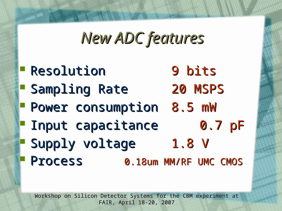
ResolutionResolution 9 bits9 bits Sampling RateSampling Rate 20 MSPS20 MSPS Power consumptionPower consumption 8.5 mW8.5 mW Input capacitanceInput capacitance 0.7 pF0.7 pF Supply voltageSupply voltage 1.8 V1.8 V ProcessProcess 0.18um MM/RF UMC CMOS0.18um MM/RF UMC CMOS
New ADC featuresNew ADC features
Workshop on Silicon Detector Systems for the CBM experiment at FAIR, April 18-20, 2007Workshop on Silicon Detector Systems for the CBM experiment at FAIR, April 18-20, 2007
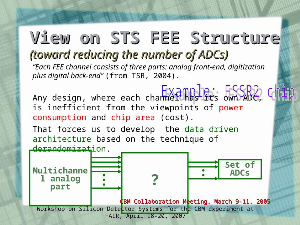
View on STS FEE StructureView on STS FEE Structure(toward reducing the number of ADCs)(toward reducing the number of ADCs)“Each FEE channel consists of three parts: analog front-end, digitization plus digital back-end” (from TSR, 2004).
Any design, where each channel has its own ADC, is inefficient from the viewpoints of power consumption and chip area (cost). That forces us to develop the data driven architecture based on the technique of derandomization.
Multichannel analog part ?
Set of ADCs
CBM Collaboration Meeting, March 9-11, 2005CBM Collaboration Meeting, March 9-11, 2005
Workshop on Silicon Detector Systems for the CBM experiment at FAIR, April 18-20, 2007Workshop on Silicon Detector Systems for the CBM experiment at FAIR, April 18-20, 2007
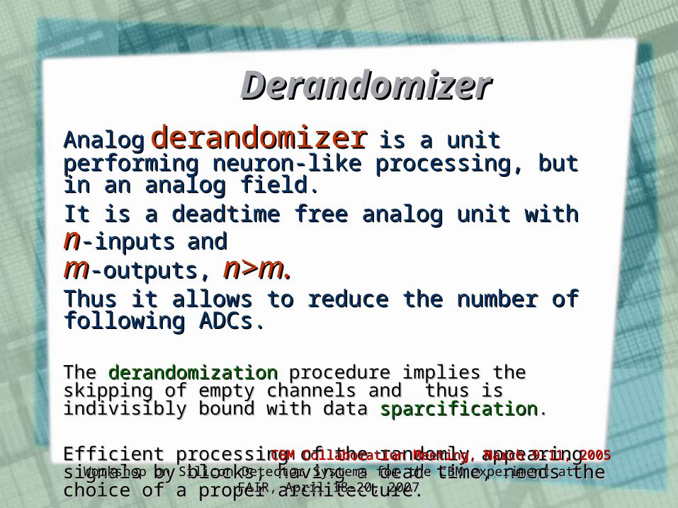
AnalogAnalog derandomizerderandomizer is a unit performing is a unit performing neuron-like processing, but in an analog field.neuron-like processing, but in an analog field.
It is a deadtime free analog unit withIt is a deadtime free analog unit with nn-inputs-inputs andand
mm-outputs,-outputs, n>m.n>m.Thus it allows to reduce the number of Thus it allows to reduce the number of following ADCs.following ADCs.
The The derandomizationderandomization procedure implies the skipping of procedure implies the skipping of empty channels and thus is indivisibly bound with data empty channels and thus is indivisibly bound with data sparcificationsparcification.. Efficient processing of the randomly appearing signals by Efficient processing of the randomly appearing signals by blocks, having a dead time, needs the choice of a proper blocks, having a dead time, needs the choice of a proper architecture.architecture.
DerandomizerDerandomizer
Workshop on Silicon Detector Systems for the CBM experiment at FAIR, April 18-20, Workshop on Silicon Detector Systems for the CBM experiment at FAIR, April 18-20, 20072007
CBM Collaboration Meeting, March 9-11, 2005CBM Collaboration Meeting, March 9-11, 2005
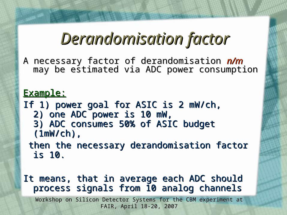
A necessary factor of derandomisation A necessary factor of derandomisation n/mn/m may may be estimated via ADC power consumptionbe estimated via ADC power consumption
Example:Example:If 1) power goal for ASIC is 2 mW/ch,If 1) power goal for ASIC is 2 mW/ch,
2) one ADC power is 10 mW, 2) one ADC power is 10 mW, 3) ADC consumes 50% of ASIC budget 3) ADC consumes 50% of ASIC budget (1mW/ch),(1mW/ch),
then the necessary derandomisation factor is 10. then the necessary derandomisation factor is 10.
It means, that in average each ADC should It means, that in average each ADC should process signals from 10 analog channelsprocess signals from 10 analog channels
Derandomisation factorDerandomisation factor
Workshop on Silicon Detector Systems for the CBM experiment at FAIR, April 18-20, 2007Workshop on Silicon Detector Systems for the CBM experiment at FAIR, April 18-20, 2007
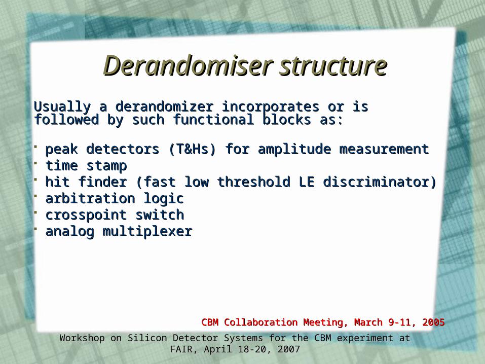
Usually a derandomizer incorporates or is followed by Usually a derandomizer incorporates or is followed by such functional blocks as:such functional blocks as: peak detectors (T&Hs) for amplitude measurementpeak detectors (T&Hs) for amplitude measurement time stamptime stamp hit finder (fast low threshold LE discriminator)hit finder (fast low threshold LE discriminator) arbitration logicarbitration logic crosspoint switchcrosspoint switch analog multiplexeranalog multiplexer
Derandomiser structureDerandomiser structure
CBM Collaboration Meeting, March 9-11, 2005CBM Collaboration Meeting, March 9-11, 2005
Workshop on Silicon Detector Systems for the CBM experiment at FAIR, April 18-20, 2007Workshop on Silicon Detector Systems for the CBM experiment at FAIR, April 18-20, 2007
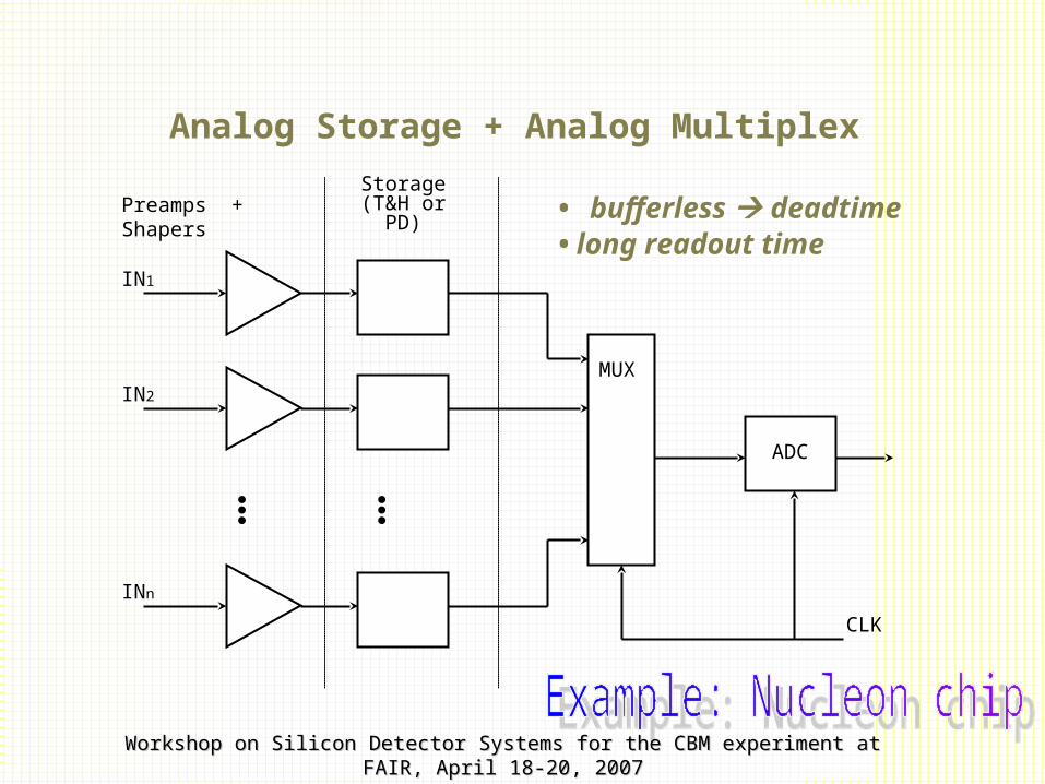
Analog Storage + Analog Multiplex
• bufferless deadtime• long readout time
Preamps + ShapersStorage(T&H or
PD)
MUX
ADC
IN1
IN2
INn
●●●
●●●
CLK
Workshop on Silicon Detector Systems for the CBM experiment at FAIR, April 18-20, 2007Workshop on Silicon Detector Systems for the CBM experiment at FAIR, April 18-20, 2007
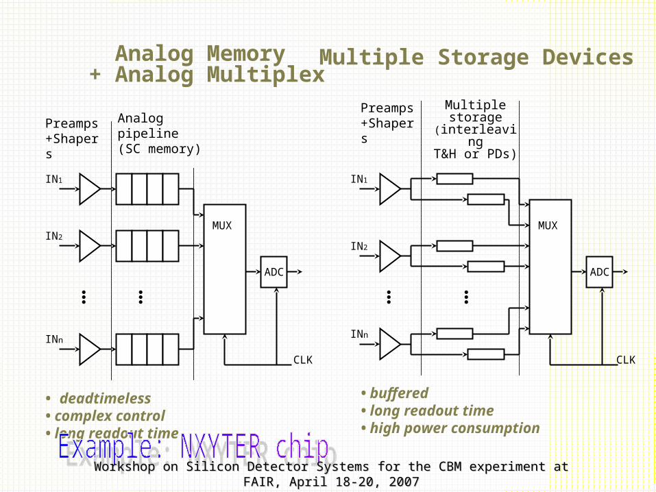
Analog Memory + Analog Multiplex
Multiple Storage Devices
●●●
●●●
Preamps+Shapers
MUX
ADC
CLK
●●●
●●●
MUX
ADC
CLK
Analog
pipeline(SC memory)
Multiplestorage
(interleavingT&H or PDs)
IN1
IN2
INn
Preamps+Shapers
IN1
IN2
INn
• deadtimeless• complex control• long readout time
• buffered• long readout time• high power consumption
Workshop on Silicon Detector Systems for the CBM experiment at FAIR, April 18-20, 2007Workshop on Silicon Detector Systems for the CBM experiment at FAIR, April 18-20, 2007
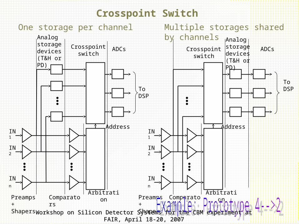
Crosspoint Switch
ToDSP
Multiple storages shared by channelsOne storage per channel
●●●
●●●
●●●
ArbitrationComparators
Crosspoint switch
ADCs
IN1
IN2
INn
ToDSP
Analogstoragedevices (T&H or PD)
Arbitration
ADCs
●●●
IN1
IN2
INn
●●●
Comparators
●●●
Preamps + Shapers
Address Address
Crosspoint switch
Analogstoragedevices (T&H or PD)
Preamps + Shapers
Workshop on Silicon Detector Systems for the CBM experiment at FAIR, April 18-20, 2007Workshop on Silicon Detector Systems for the CBM experiment at FAIR, April 18-20, 2007
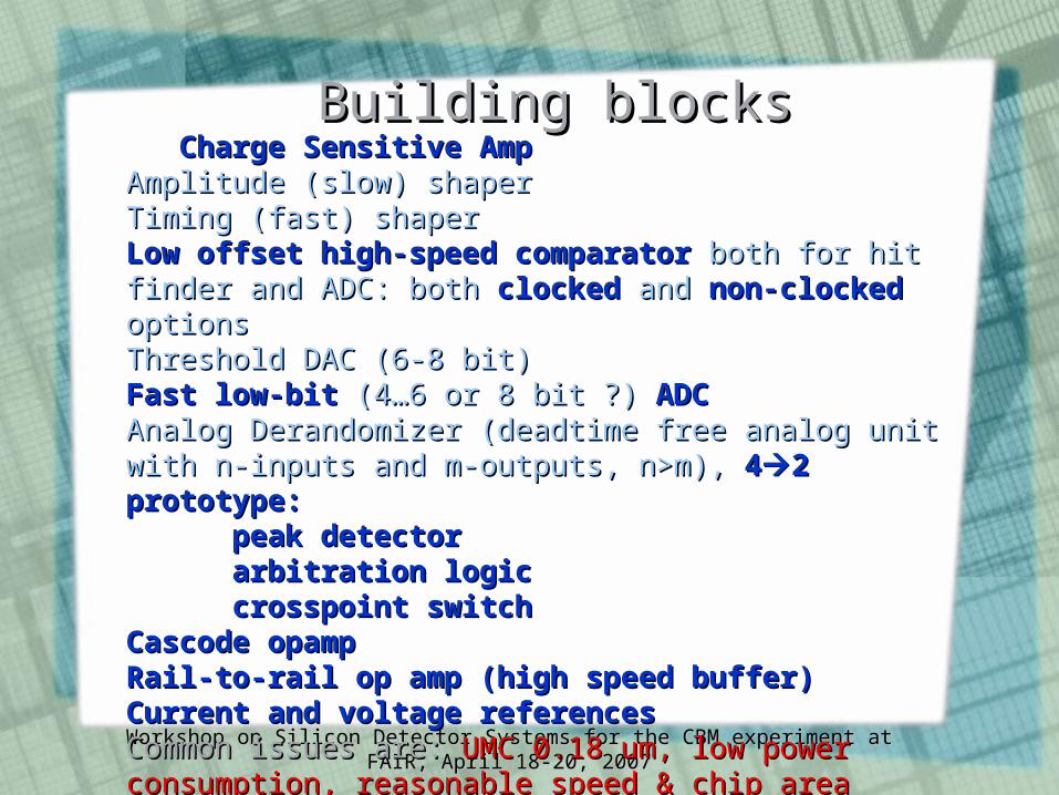
Building blocksBuilding blocks
Workshop on Silicon Detector Systems for the CBM experiment at FAIR, April 18-20, 2007Workshop on Silicon Detector Systems for the CBM experiment at FAIR, April 18-20, 2007
Charge Sensitive AmpCharge Sensitive AmpAmplitude (slow) shaperAmplitude (slow) shaperTiming (fast) shaperTiming (fast) shaperLow offset high-speed comparatorLow offset high-speed comparator both for hit both for hit finder and ADC: both finder and ADC: both clockedclocked and and non-clocked non-clocked optionsoptionsThreshold DAC (6-8 bit)Threshold DAC (6-8 bit)Fast low-bitFast low-bit (4…6 or 8 bit ?) (4…6 or 8 bit ?) ADCADCAnalog Derandomizer (deadtime free analog unit with Analog Derandomizer (deadtime free analog unit with n-inputs and m-outputs, n>m), n-inputs and m-outputs, n>m), 442 prototype:2 prototype:
peak detectorpeak detectorarbitration logicarbitration logiccrosspoint switchcrosspoint switch
Cascode opampCascode opampRail-to-rail op amp (high speed buffer)Rail-to-rail op amp (high speed buffer)Current and voltage referencesCurrent and voltage referencesCommon issues are: Common issues are: UMC 0.18 um, low power UMC 0.18 um, low power consumption, reasonable speed & chip areaconsumption, reasonable speed & chip area
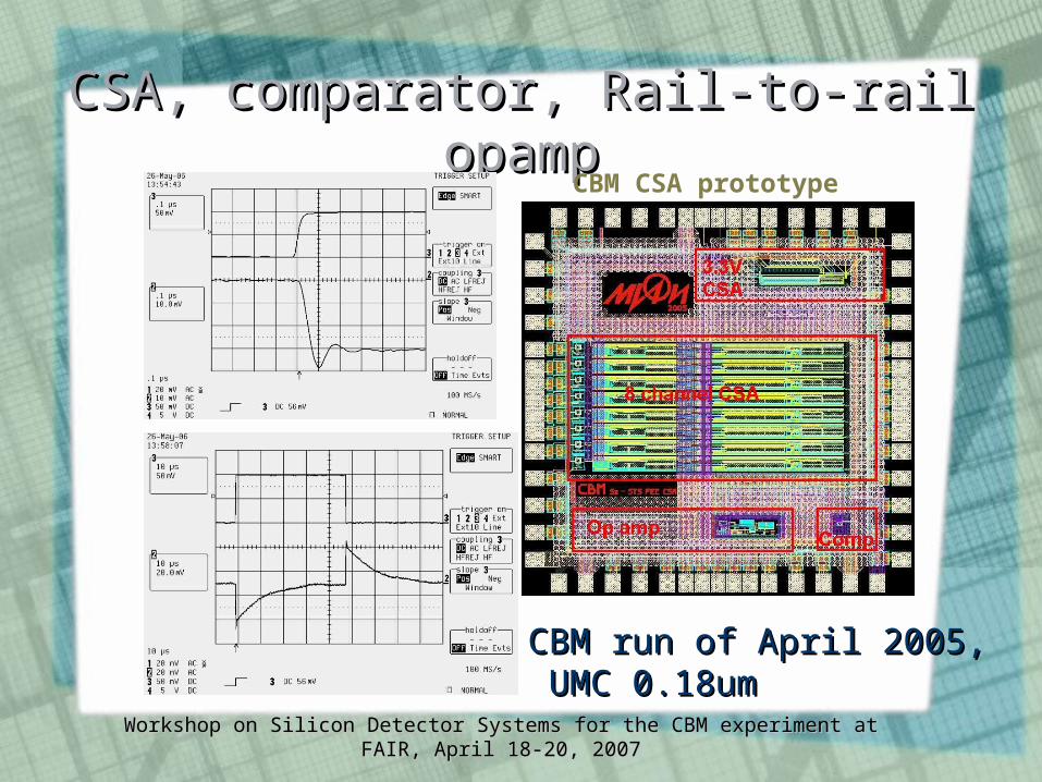
CSA, comparator, Rail-to-rail opampCSA, comparator, Rail-to-rail opamp
CBM run of April 2005,CBM run of April 2005, UMC 0.18umUMC 0.18um
CBM CSA prototype
Workshop on Silicon Detector Systems for the CBM experiment at FAIR, April 18-20, 2007Workshop on Silicon Detector Systems for the CBM experiment at FAIR, April 18-20, 2007
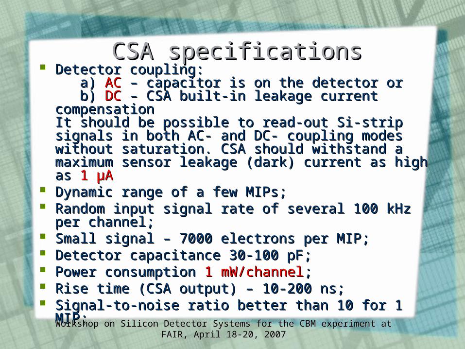
CSA specificationsCSA specifications Detector coupling:Detector coupling:
a) a) ACAC – capacitor is on the detector or – capacitor is on the detector or b) b) DCDC – CSA built-in leakage current – CSA built-in leakage current compensationcompensationIt should be possible to read-out Si-strip signals It should be possible to read-out Si-strip signals in both AC- and DC- coupling modes without in both AC- and DC- coupling modes without saturation. CSA should withstand a maximum saturation. CSA should withstand a maximum sensor leakage (dark) current as high as sensor leakage (dark) current as high as 1 1 μμAA
Dynamic range of a few MIPs;Dynamic range of a few MIPs; Random input signal rate of several 100 kHz Random input signal rate of several 100 kHz
per channel;per channel; Small signal – 7000 electrons per MIP;Small signal – 7000 electrons per MIP; Detector capacitance 30-100 pF;Detector capacitance 30-100 pF; Power consumption Power consumption 1 mW/channel1 mW/channel;; Rise time (CSA output) – 10-200 ns;Rise time (CSA output) – 10-200 ns; Signal-to-noise ratio better than 10 for 1 MIP;Signal-to-noise ratio better than 10 for 1 MIP;Workshop on Silicon Detector Systems for the CBM experiment at FAIR, April 18-20, 2007Workshop on Silicon Detector Systems for the CBM experiment at FAIR, April 18-20, 2007
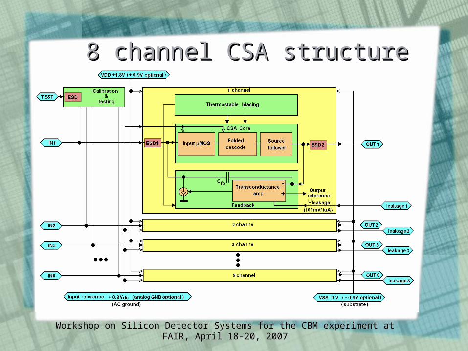
8 channel CSA structure8 channel CSA structure
Workshop on Silicon Detector Systems for the CBM experiment at FAIR, April 18-20, 2007Workshop on Silicon Detector Systems for the CBM experiment at FAIR, April 18-20, 2007
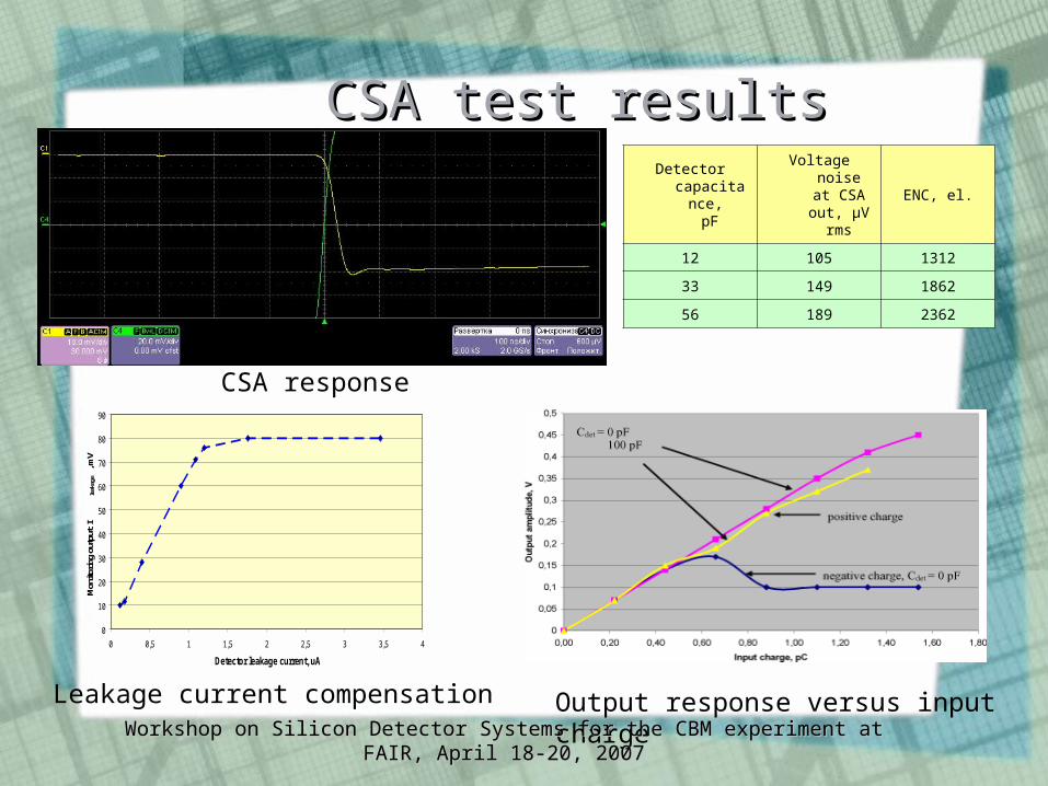
CSA test resultsCSA test results
0
10
20
30
40
50
60
70
80
90
0 0,5 1 1,5 2 2,5 3 3,5 4
Detector leakage current, uA
Mon
itorin
g ou
tput
Ile
akag
e, m
V
Detector capacitanc
e, pF
Voltage noise at CSA out, µV
rms
ENC, el.
12 105 1312
33 149 1862
56 189 2362
CSA response
Output response versus input chargeLeakage current compensation
Workshop on Silicon Detector Systems for the CBM experiment at FAIR, April 18-20, 2007Workshop on Silicon Detector Systems for the CBM experiment at FAIR, April 18-20, 2007
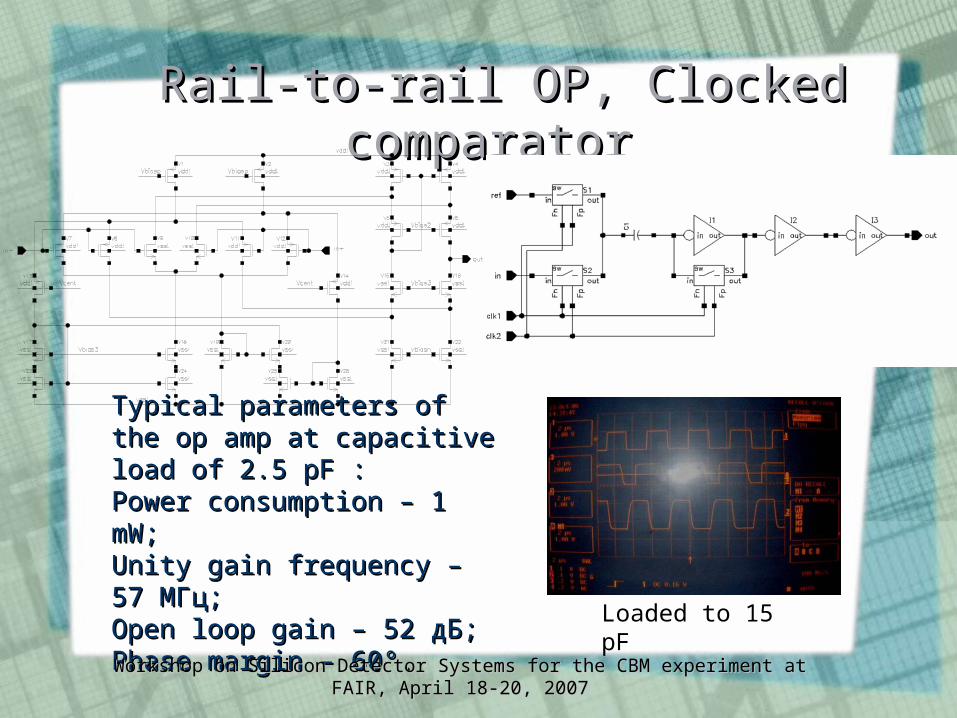
Rail-to-rail OP, Clocked Rail-to-rail OP, Clocked comparatorcomparator
Typical parameters of the op Typical parameters of the op amp at capacitive load of 2.5 amp at capacitive load of 2.5 pF :pF :Power consumption – 1 mW;Power consumption – 1 mW;Unity gain frequency – 57 Unity gain frequency – 57 МГцМГц;;Open loop gain – 52 Open loop gain – 52 дБдБ;;Phase margin – 60°.Phase margin – 60°.
Loaded to 15 pF
Workshop on Silicon Detector Systems for the CBM experiment at FAIR, April 18-20, 2007Workshop on Silicon Detector Systems for the CBM experiment at FAIR, April 18-20, 2007
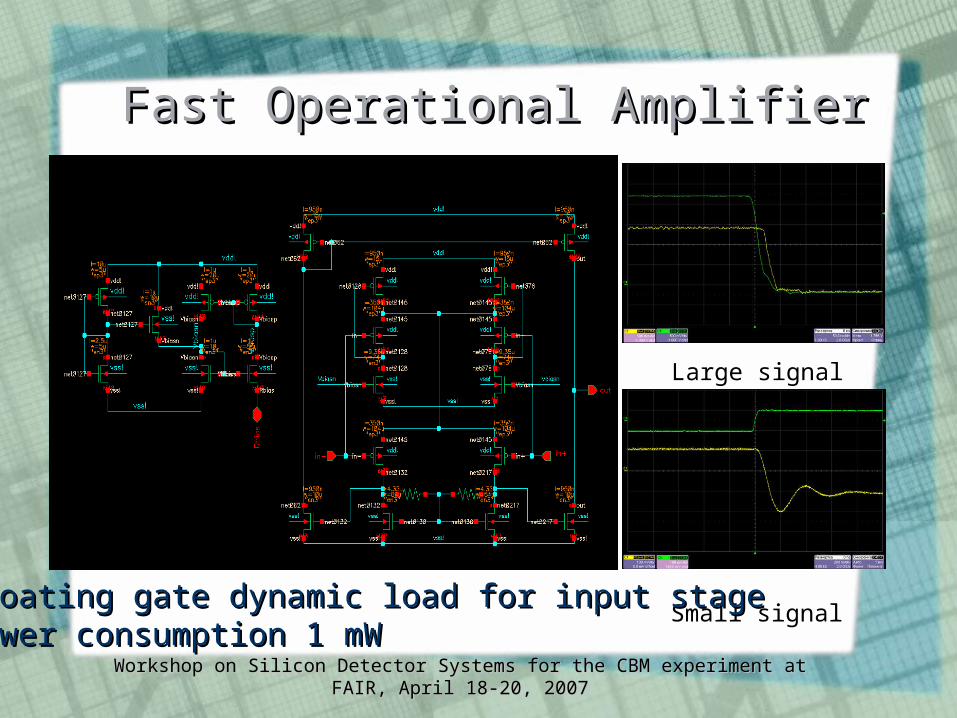
Fast Operational AmplifierFast Operational Amplifier
Large signal
Small signalFloating gate dynamic load for input stageFloating gate dynamic load for input stagePower consumption 1 mWPower consumption 1 mW
Workshop on Silicon Detector Systems for the CBM experiment at FAIR, April 18-20, 2007Workshop on Silicon Detector Systems for the CBM experiment at FAIR, April 18-20, 2007
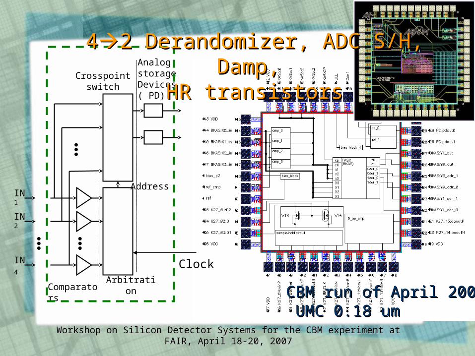
Arbitration
●●●
IN1
IN2
IN4
●●●
Comparators
●●●
Address
Crosspoint switch
AnalogstorageDevices( PD)
Clock
CBM run of April 2006,CBM run of April 2006, UMC 0.18 umUMC 0.18 um
Workshop on Silicon Detector Systems for the CBM experiment at FAIR, April 18-20, 2007Workshop on Silicon Detector Systems for the CBM experiment at FAIR, April 18-20, 2007
442 Derandomizer, ADC S/H, Damp, 2 Derandomizer, ADC S/H, Damp, HR transistorsHR transistors
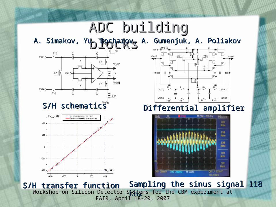
S/H schematicsS/H schematics Differential amplifierDifferential amplifier
Sampling the sinus signal 118 kHzSampling the sinus signal 118 kHzS/H transfer functionS/H transfer function
ADC building blocksADC building blocksA. Simakov, Yu. Bocharov, A. Gumenjuk, A. PoliakovA. Simakov, Yu. Bocharov, A. Gumenjuk, A. Poliakov
Workshop on Silicon Detector Systems for the CBM experiment at FAIR, April 18-20, 2007Workshop on Silicon Detector Systems for the CBM experiment at FAIR, April 18-20, 2007
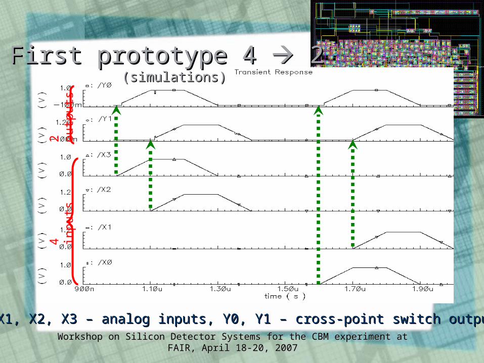
X0, X1, X2, X3 – analog inputs, Y0, Y1 – cross-point switch outputs X0, X1, X2, X3 – analog inputs, Y0, Y1 – cross-point switch outputs
Workshop on Silicon Detector Systems for the CBM experiment at FAIR, April 18-20, 2007Workshop on Silicon Detector Systems for the CBM experiment at FAIR, April 18-20, 2007
First prototype 4 First prototype 4 2 2 (simulations)(simulations)
4 inp
uts
2
ou
tputs
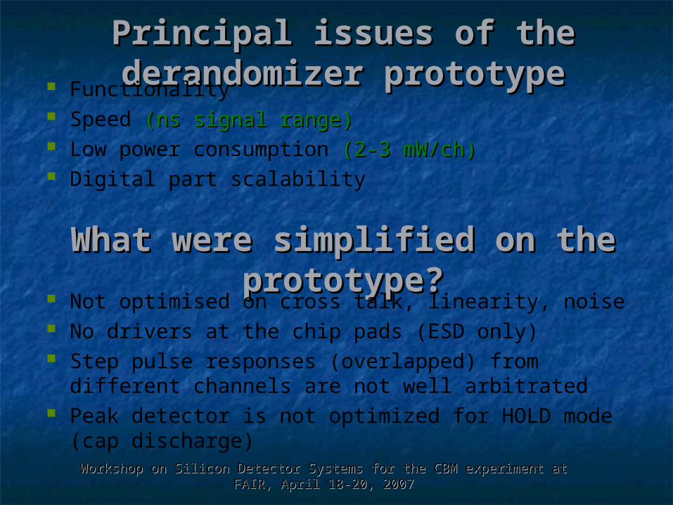
What were simplified on the What were simplified on the prototype?prototype?
Not optimised on cross talk, linearity, noise No drivers at the chip pads (ESD only) Step pulse responses (overlapped) from different
channels are not well arbitrated Peak detector is not optimized for HOLD mode
(cap discharge)
Principal issues of the Principal issues of the derandomizer prototypederandomizer prototype Functionality
Speed (ns signal range)(ns signal range) Low power consumption (2-3 mW/ch)(2-3 mW/ch) Digital part scalability
Workshop on Silicon Detector Systems for the CBM experiment at FAIR, April 18-20, 2007Workshop on Silicon Detector Systems for the CBM experiment at FAIR, April 18-20, 2007
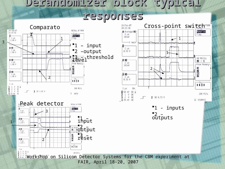
Derandomizer block typical Derandomizer block typical responsesresponses
1 – input2 –output3 – threshold level
1
2
3
1 - inputs2 – outputs
1
1
2
Comparator Cross-point switch
2
3
Peak detector
1
Workshop on Silicon Detector Systems for the CBM experiment at FAIR, April 18-20, 2007Workshop on Silicon Detector Systems for the CBM experiment at FAIR, April 18-20, 2007
1 – input2 –output3 – reset
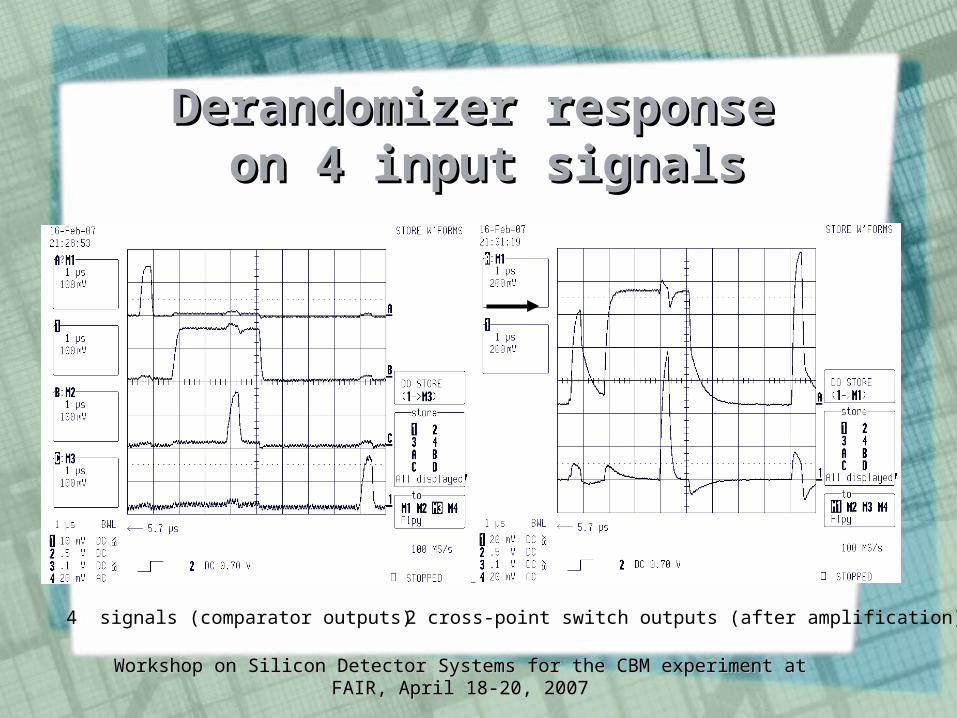
Derandomizer response Derandomizer response on 4 input signalson 4 input signals
4 signals (comparator outputs) 2 cross-point switch outputs (after amplification)
Workshop on Silicon Detector Systems for the CBM experiment at FAIR, April 18-20, 2007Workshop on Silicon Detector Systems for the CBM experiment at FAIR, April 18-20, 2007
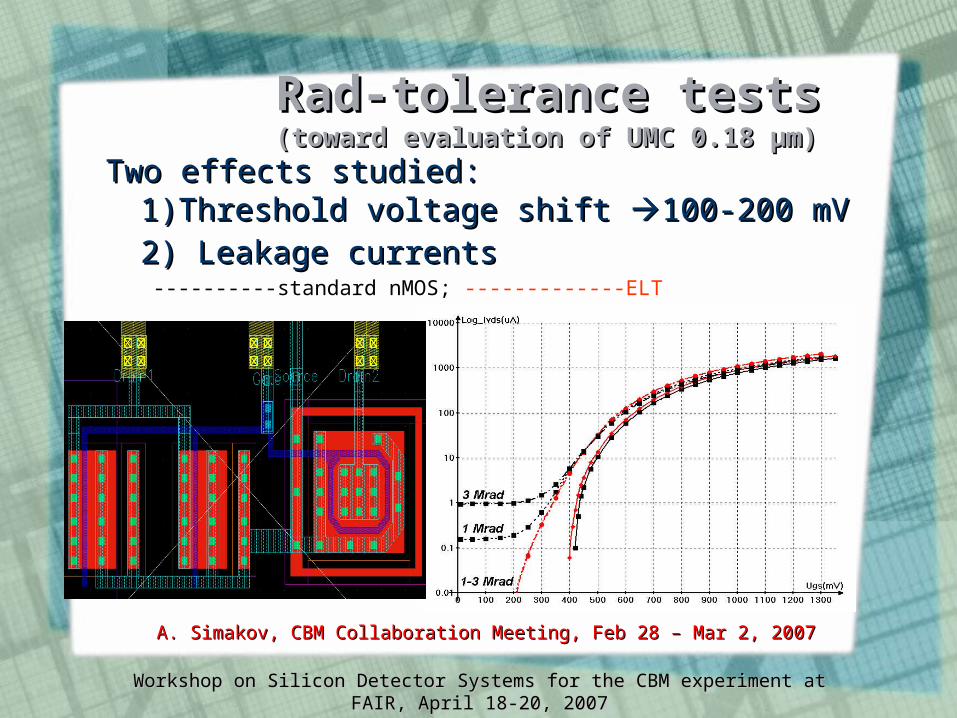
Two effects studied:Two effects studied: 1)Threshold voltage shift 1)Threshold voltage shift 100-200 mV100-200 mV2) Leakage currents2) Leakage currents
----------standard nMOS; -------------ELT
Rad-tolerance testsRad-tolerance tests(toward evaluation of UMC 0.18 µm(toward evaluation of UMC 0.18 µm))
A. Simakov, CBM Collaboration Meeting, Feb 28 – Mar 2, 2007A. Simakov, CBM Collaboration Meeting, Feb 28 – Mar 2, 2007
Workshop on Silicon Detector Systems for the CBM experiment at FAIR, April 18-20, 2007Workshop on Silicon Detector Systems for the CBM experiment at FAIR, April 18-20, 2007
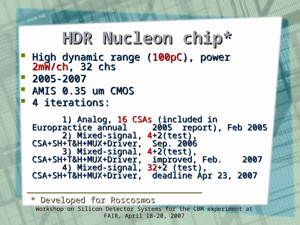
HDR Nucleon chip*HDR Nucleon chip* High dynamic range (High dynamic range (100pC100pC), power ), power 2mW/ch2mW/ch, ,
32 chs 32 chs 2005-20072005-2007 AMIS 0.35 um CMOSAMIS 0.35 um CMOS 4 iterations:4 iterations:
1) Analog, 1) Analog, 16 CSAs16 CSAs (included in Europractice (included in Europractice annual annual 2005 2005 report), Feb 2005report), Feb 2005
2) Mixed-signal, 2) Mixed-signal, 44+2(test), +2(test), CSA+SH+T&H+MUX+Driver, CSA+SH+T&H+MUX+Driver, Sep. 2006Sep. 2006
3) Mixed-signal, 3) Mixed-signal, 44+2(test), +2(test), CSA+SH+T&H+MUX+Driver, CSA+SH+T&H+MUX+Driver, improved, Feb. improved, Feb.
200720074) Mixed-signal, 4) Mixed-signal, 3232+2 (test), +2 (test),
CSA+SH+T&H+MUX+Driver, CSA+SH+T&H+MUX+Driver, deadline Apr 23, deadline Apr 23, 20072007* Developed for Roscosmos* Developed for Roscosmos
Workshop on Silicon Detector Systems for the CBM experiment at FAIR, April 18-20, 2007Workshop on Silicon Detector Systems for the CBM experiment at FAIR, April 18-20, 2007
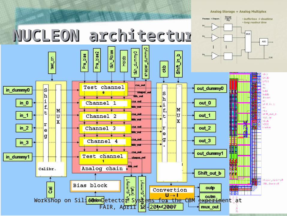
NUCLEON architectureNUCLEON architecture
Workshop on Silicon Detector Systems for the CBM experiment at FAIR, April 18-20, 2007Workshop on Silicon Detector Systems for the CBM experiment at FAIR, April 18-20, 2007
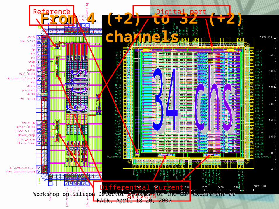
From 4 (+2) to 32 (+2) From 4 (+2) to 32 (+2) channelschannels
Differential Current drivers
Digital partReferences
Workshop on Silicon Detector Systems for the CBM experiment at FAIR, April 18-20, 2007Workshop on Silicon Detector Systems for the CBM experiment at FAIR, April 18-20, 2007
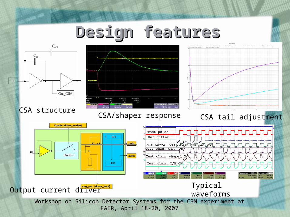
Design featuresDesign features
CSA structure
Output current driver
CSA/shaper response
Typical waveforms
CSA tail adjustment
Workshop on Silicon Detector Systems for the CBM experiment at FAIR, April 18-20, 2007Workshop on Silicon Detector Systems for the CBM experiment at FAIR, April 18-20, 2007
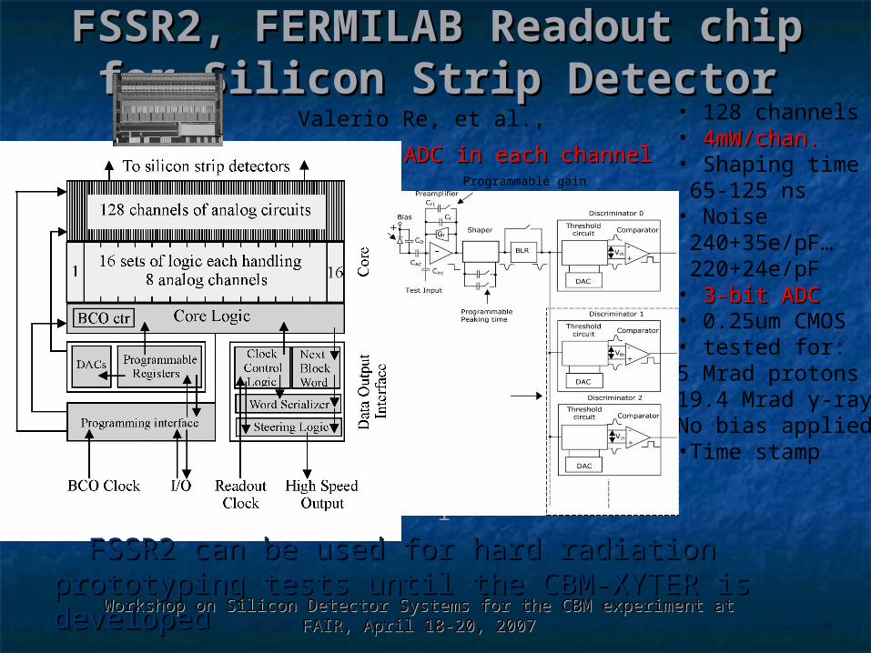
FSSR2, FERMILAB Readout FSSR2, FERMILAB Readout chip for Silicon Strip Detectorchip for Silicon Strip Detector
Valerio Re, et al., • 128 channels• 4mW/chan.4mW/chan.• Shaping time 65-125 ns• Noise 240+35e/pF… 220+24e/pF• 3-bit ADC3-bit ADC • 0.25um CMOS• tested for:5 Mrad protons19.4 Mrad γ-raysNo bias applied •Time stamp
Flash ADC
Programmable gain
• FSSR2 can be used for hard radiation prototyping FSSR2 can be used for hard radiation prototyping tests until the CBM-XYTER is developedtests until the CBM-XYTER is developed
One analog channel
Workshop on Silicon Detector Systems for the CBM experiment at FAIR, April 18-20, 2007Workshop on Silicon Detector Systems for the CBM experiment at FAIR, April 18-20, 2007
ADC in each channelADC in each channel
OutlooksOutlooks
Developed are different building blocks Developed are different building blocks mostly in UMC 0.18 and partially in AMIS 0.35 mostly in UMC 0.18 and partially in AMIS 0.35
We are thinking about incorporating them into We are thinking about incorporating them into the CBM-XYTERthe CBM-XYTER
We are looking forward to request R&D We are looking forward to request R&D money from RF Ministriesmoney from RF Ministries
Workshop on Silicon Detector Systems for the CBM experiment at FAIR, April 18-20, 2007Workshop on Silicon Detector Systems for the CBM experiment at FAIR, April 18-20, 2007