Overview of Rigid Flex Technology - SMTA · PDF fileOverview of Rigid Flex Technology. ......
82
Joseph Fjelstad Overview of Rigid Flex Technology
Transcript of Overview of Rigid Flex Technology - SMTA · PDF fileOverview of Rigid Flex Technology. ......

Joseph Fjelstad
Overview of Rigid Flex Technology

Background
Flexible circuits have seen explosive growth in recent times
owing to their numerous advantages as an interconnection
medium.
Presently nearly every imaginable type of electronic product
employs flex.
The technology requires understanding in order to assure
successful deployment.
This is especially true for rigid flex variants.

Rigid Flex Advantages
Rigid Flex interconnection technologies enable design freedom
unmatched by more traditional rigid interconnection methods and the
applications are rapidly expanding
Integrating more technology into less material and space is a key
technological objective but it has many other benefits
Newer materials, structural concepts and manufacturing processes will
open doors to future products that will improve our communications,
entertain, transport, protect and inform us but could also redefine
medical technology and aid in scientific discovery.
Flexible electronic Interconnections will play an expanding role in the
future of electronics and rigid flex will have an increasing role

Rigid Flex Issues
Several approaches have been use since the 1970s for rigid flex
Rigid flex can reduce overall complexity and increase reliability
However, the cost for rigid flex is greater than for either rigid or flex due to a number of factors
- PI flex materials more expensive than FR4 laminates (~ 3X)
- Low flow adhesives normally are more costly than epoxy prepreg
- Coverlayers and flexible cover coats also cost more than standard solder masks
- Design and process planning are often engineering time intensive
- Manufacturing is labor intensive, some equipment is unique and rigid flex is not readily adapted to automation.
Still from a system perspective, rigid flex can save time and money

Rigid Flex Constructions

Origins…

Rigid Flex… Nearing 50 Years of Use

Rigid Flex Applications

Rigid Flex Circuit Applications
Rigid flex circuits were developed largely to replace bulky and heavy
wire harnesses but have since migrated to many new areas of application
Clam shell type mobile phones
Mobile phone camera modules
Missiles and weapons systems
Camera monitoring systems
Electrical test equipment
Lap top computers
Digital cameras
Hearing Aids
Satellites

A Few Rigid Flex Examples

CCD Detector
Source : University of Texas

Hand Held Key Board Assembly
Source : Interconnect Systems, Inc.
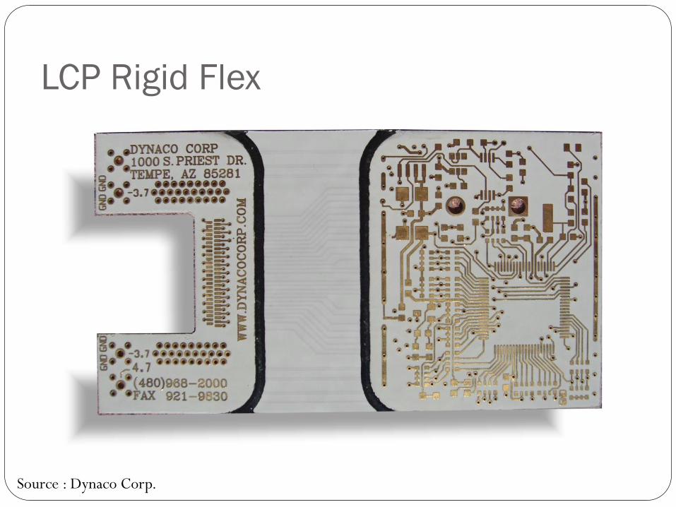
Source : Dynaco Corp.
LCP Rigid Flex

COB on Rigid Flex
Source : University of Pennsylvania

Representative
Rigid Flex Constructions

Traditional
Rigid Flex
Structure
Coverlayer
extends over all
Internal circuitry
Exemplary Rigid Flex Constructions
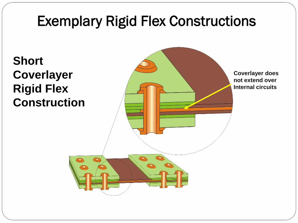
Short
Coverlayer
Rigid Flex
Construction
Coverlayer does
not extend over
Internal circuits
Exemplary Rigid Flex Constructions

Hybrid
Laminate
Rigid Flex
Construction
Copper foil covers
lapped rigid and
flexible materials
Exemplary Rigid Flex Constructions

Surface Flex
Rigid Flex
Construction
Flex circuit on outer
surfaces only
Exemplary Rigid Flex Constructions
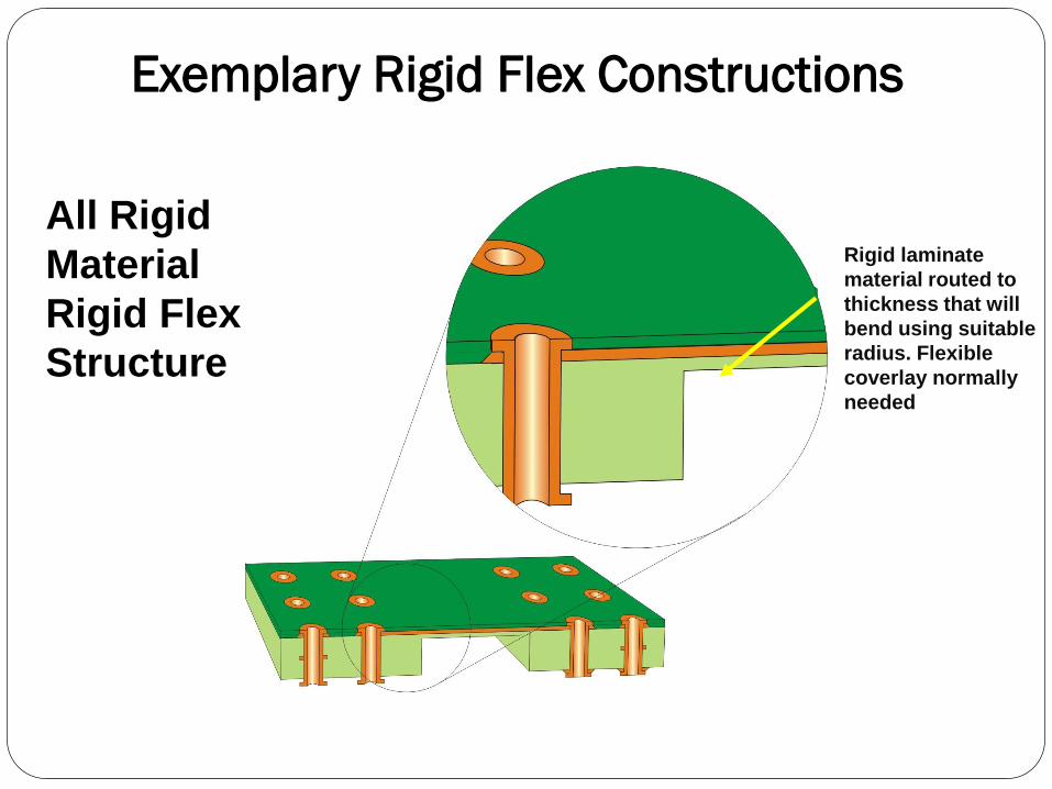
Exemplary Rigid Flex Constructions
All Rigid
Material
Rigid Flex
Structure
Rigid laminate
material routed to
thickness that will
bend using suitable
radius. Flexible
coverlay normally
needed

Reinforced Flex Construction
(Not a rigid flex)
Flex circuit bonded to
rigid stiffener

The Basic Process
1. Double-sided flex is built
with coverlayer but no holes
2. Rigid caps are scored for later
removal and laminated to flex
using bondply or pre-preg
3. Circuit is drilled and processed
like standard multilayer circuit
After routing the scored areas are
removed to allow circuit to flex
Note: Conceptually representative only… Many steps are missing

Other Solutions and Issues
Thin or thinned FR4 circuits can be bent.
Semi-rigid laminates with non woven reinforcement materials
and lower modulus thermoplastic resins (e.g. PTFE, polyester
etc.) have been explored and could be revisited.
The rub is that when it comes to assembly, used of high
temperature lead-free solders will be cause for continuing
concern to the industry owing to the higher Z axis CTE
inherent with more commonly used design and manufacturing
approaches for rigid flex structures.

Tacky Carrier for Flex SMT Assembly
•Metal carrier plate can be cut to size
•Adhesive is a tacky high temperature silicone
•Lead-free solder capable
•Durable withstanding multiple reflow passes
•Provides ESD protection
•Easy removal after assembly
•Can be cleaned and reused
•Can be modified for two side SMT assembly

Flex SMT Assembly Aids
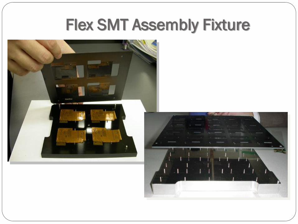
Flex SMT Assembly Fixture

Rigid Flex Assembly

Rigid Flex Assembly

Rigid Flex Assembly

Bulkhead Connector Assembly
Tiered pins with
trimmed flex soldered
to connector in
sequence
Pins untrimmed and
each layer of
interconnect soldered
sequentially.
Clearance holes
provided on each
layer for non interconnecting pins
Flex circuit lap
soldered to
connector pins
Flex for layered connections

Integral Connection Options
Fitted with Connector Elements
Supported Edge Connection
Crimped Pin / SocketConnector
Staked PinConnector
Straight or Formed Pin
Connector
Commercial Mated Pair Connector
Unsupported Edge Connection
Lapped Edge Connection
Integral Connections
Solder Alloy Free Electronics
(SAFE)
Rigid Flex Options

The Punishment of Sisyphus

Soldering Fishbone Diagram
Source: Interphase Corporation

Question:
Is Solder Necessary
for Electronic Assembly?
Base Material

Machine, Mold or Etch Cavities

Place Components in Cavities

Coat with RCC or Alternative

Prepare Flex Circuit and Bondply
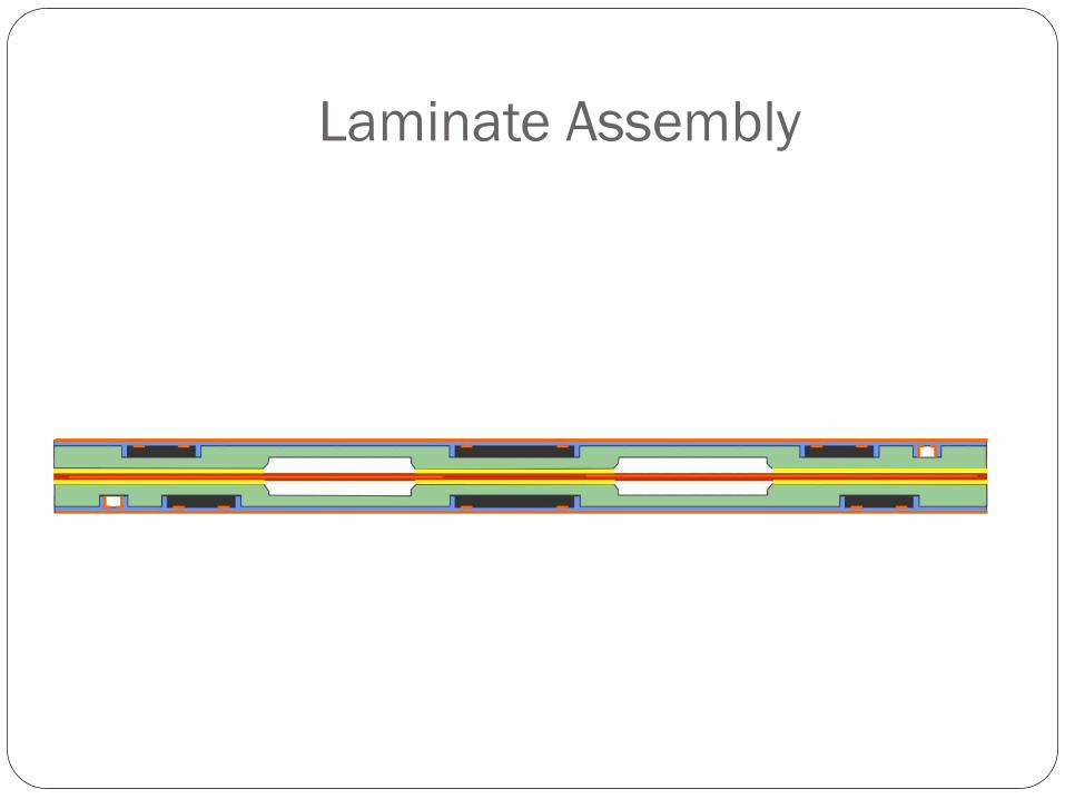
Laminate Assembly

Drill Through Holes and Vias

Plate Assembly and Thru Holes

Image and EtchAlternative Methods Possible

Expose Flex By Design

Form Circuit

Molded Solderless Rigid Flex Assembly Type I

Molded Solderless Rigid Flex Assembly Type II

Over Molded RigidFlex Assembly Type III
Patents Pending

Metal Rigid Flex Assembly (1)
Assemble components to substrate to create modules for product
Encapsulate assembly
Singulate modules

Metal Rigid Flex Assembly (2)
Place modules (or discrete components) into machined aluminum carrier
Cure adhesive
Laminate flexible material and create vias to access lands

Metal Rigid Flex Assembly (3)
Additively create circuits to required layer count needed for design
Laminate converlayer
Machine (or chemically mill) excess aluminum

Metal Rigid Flex Assembly (4)
Apply etch resist
Etch exposed aliminum
Apply strain relief

Metal Rigid Flex Assembly (5)
Form to desired shape
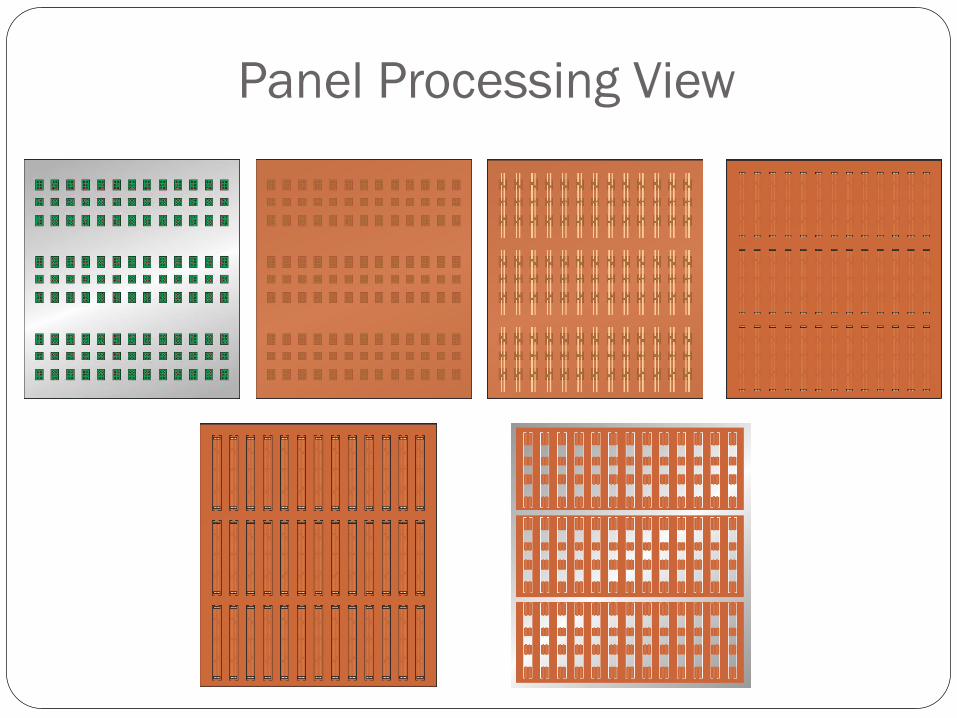
Panel Processing View

Aluminum Core
Rigid Flex Processing

Aluminum Assembly Basics
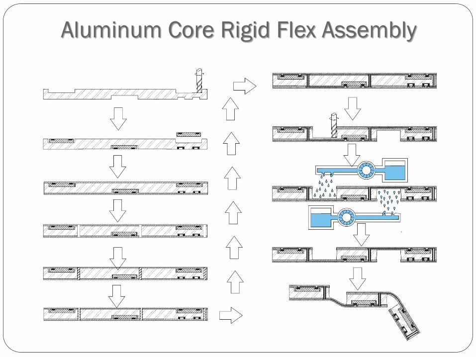
Aluminum Core Rigid Flex Assembly

Solderless Redesign Exercise

Solderless Redesign Exercise
From Rigid to Rigid Flex
140 x 100mm 12 layer rigid board442 FPGA 0.8mm pitch
6 layer Aluminum Rigid-flex Assy ~30mm X 40mm (when folded)All components on 0.5mm pitch50mm line/space with 50mm vias

• Design is ~70% smaller in terms of total area • Folds into an assembly with footprint ~15% of
original design with minimal increase in height. • Though the density of aluminum is higher than
FR4, (FR4=1.8 gr/cm3, Al=2.7gr/cm) the total weight of the assembly is projected to be ~55-65% less than the original.
• Rigid flex structure is amenable to the separation of digital and analog circuity and thus the potential for better control of the energy created by analog devices and power supplies.
Design Comparison Details
Stretchable
Rigid Flex Circuit

Out of Plane Stretching
Methods from the Past
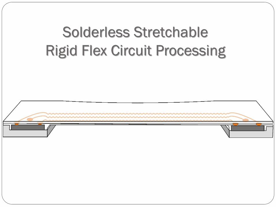
Solderless Stretchable
Rigid Flex Circuit Processing

Rapid Prototyping

Direct Write Prototyping
without Solder
Patents Pending
With parts in hand, first prototypes could possibly be
completed in hours rather than days, weeks or months
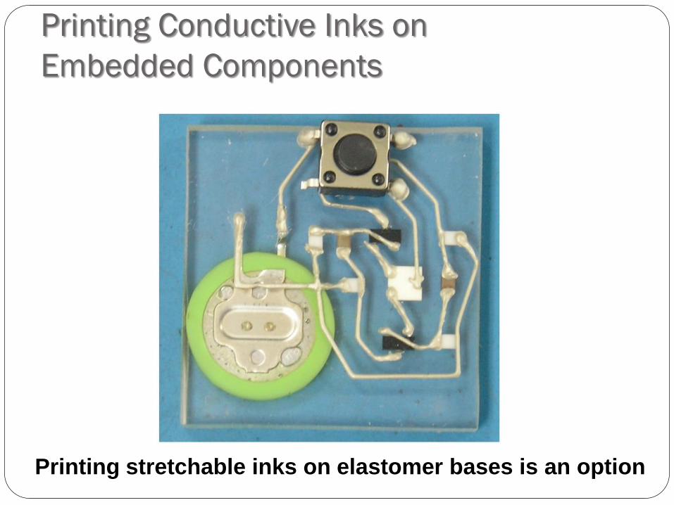
Printing Conductive Inks on
Embedded Components
Printing stretchable inks on elastomer bases is an option

Solderless
Assembly
Benefits

No procurement
No testing required
No inventory or shelf life concern
No CAF concern
No surface finish process durability issues
No high temperature warp or board damage
Lower overall material use
All copper circuits created in situ
Assembly is still edge card capable
No Printed Circuit Required

Eliminates many manufacturing process steps
RoHS restricted material concerns eliminated
No solderability testing or surface finish concerns
No high temperature damage to devices
Energy use is reduced (no bakes or reflow)
No solder shorts, opens, micro voids, copper dissolution
and the host of other common solder related reliability
issues and concerns
Limited post cleaning and testing concerns
No Soldering Required

Traditional Process Steps Design PCB Assembly Fabricate PCB (multilayer) Assemble PCB
1. Create schematic
2. Indentify components
3. Layout circuits
4. Validate signal integrity
5. Validate design DfM
6. Validate design DfR
7. Validate design DfE
1. Verify RoHS compliance
2. Cut core laminas to size & tool
3. Clean and coat with resist
4. Image and develop resist
5. Etch and strip resist
6. Treat exposed copper
7. AOI or visual inspect layers
8. Cut B-stage to size and tool
9. Lay up core and B-stage
10. Laminate
11. X-ray inspect (optional)
12. Drill (stack height varies)
13. Desmear or etchback
14. Sensitize holes
15. Plate electroless copper
16. Clean and coat with resist
17. Image an develop resist
18. Pattern plate copper
19. Pattern plate metal resist
20. Strip plating resist
21. Etch base copper
22. Clean and coat with soldermask
23. Image and develop
24. Treat exposed metal (options)
25. Solder, NiAu, Sn, Ag, OSP, etc.
26. Electrical test
27. Route to shape
28. Package
29. Ship
1. Procure components
2. Verify RoHS compliance
3. Verify component solderability
4. Verify component MSL number
5. Kit components
6. Procure PCBs
7. Verify RoHS compliance
8. Verify PCB solderability
9. Verify PCB High Temp capability
10. Design solder stencil & purchase
11. Develop suitable reflow profile
12. Track component exposure (MSL)
13. (Rebake components as required)
14. Position PCB & stencil solder paste
15. (monitor solder paste)
16. Inspect solder paste results
17. (height and skips)
18. Dispense glue dots (optional)
19. Place components
20. Inspect for missing parts
21. Reflow solder
22. Repeat Steps 13-18 if two sided assy
23. (second set of fixtures required)
24. Perform hand assembly as required
25. (odd sized or temperature sensitive)
26. Clean flux from surface and under
27. Verify low standoff devices
28. Test cleanliness
29. Underfill critical components
30. X-ray inspect soldered assembly
31. Identify shorts, opens, voids, missing
32. Electrically test
33. Rework and repair as needed
34. Package
35. Ship

Only fully tested and protected components used
No solder balls or lead frames (preferred)
Fewer component types needed (LGA & QFN)
Smaller component libraries possible (Pkg types)
Leadless components = No co-planarity issues
No solder build up on tester/socket contacts
Lower cost (simpler) & higher yield on devices
No MSL issues or popcorning concerns
Improved routing for area array IC packages
Reduced Component Concerns

Components can be placed closer together
Components can be placed beneath (atop) each other
Increased routing capability
Improved design security potential
Integral heat spreader redefines placement rules
Assemblies can interconnected in X, Y & Z planes
Vertical bussing protocol opportunities
Adaptable to optoelectronics
Circuit Design Advantages
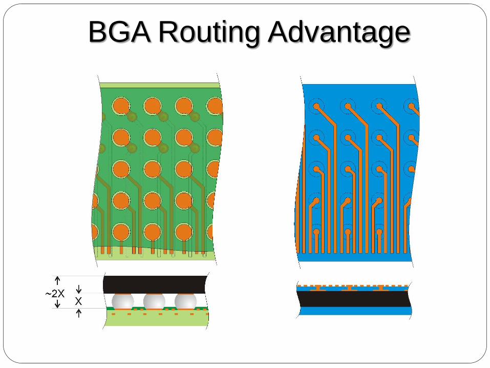
BGA Routing Advantage

Registered Package Thicknesses

One Grid Pitch or Many?

“Bite Sizing” the Challenge
Simple structures with fewer elements
Lower temperature processing avoids thermal damage
caused by high temperature soldering
Components are fully encapsulated increasing shock and
vibration immunity
Hermetic structure possibilities (plated metal jacket)
Total EMI and ESD protection possibilities
Integral heat spreader improves device life
Reliability Improvement

Testing is believed to be critical… Why?
Most testing is predicated on the anticipation of
manufacturing related defects and faults
Shorts and opens are accepted as facts of life
Lead-free assembly damage to assembly components
Current assembly technology has limits
Simpler processes should yield higher
The ultimate test is assembly turn on
Can time and money for test be better allocated?
What about Testing?

Future of Rigid Flex Integration of rigid and flex should see increased use and
application in the future
Each technology has intrinsic benefits and the synergy of the combination is highly compelling
New structures will offer and should provide significant opportunities and improvements over current generation solutions.
Unfortunately the crystal ball has not yet been perfected so the rate of adoption cannot be predicted.
Summary Rigid flex circuits are varied and versatile and continue to rise in importance in the realm
of electronic interconnections
Because of the greater levels of engineering required, the cost for more complex
structures will be higher but on a system level, the circuits will often prove a more cost
effective solution.
The product designer must understand both electrical and mechanical issues for success
New concepts for manufacture of rigid flexible and stretchable circuits have been
presented for consideration and it is believed that the economics are compelling.
While legacy components can be used, the structures are most easily realized using low
profile components of common height.
It is paradoxical that achieving simplicity in design often requires more discipline than
complexity.
Change is inevitable but adapting to, managing and controlling change is a choice.

“A mind, once stretched by a new idea, never returns to its original dimensions.”
Oliver Wendell Holmes
American Philosopher and Jurist