Overview of Materials Qualification Needs for …...Overview of Materials Qualification Needs for...
18
Overview of Materials Qualification Needs for Metal Additive Manufacturing MOHSEN SEIFI , 1,5 AYMAN SALEM, 2 JACK BEUTH, 3 OLA HARRYSSON, 4 and JOHN J. LEWANDOWSKI 1 1.—Department of Materials Science and Engineering, Case Western Reserve University, Clev- eland, USA. 2.—Materials Resources LLC, Dayton, OH, USA. 3.—Department of Mechanical Engineering, Carnegie Mellon University, Pittsburgh, USA. 4.—Department of Industrial and Systems Engineering, North Carolina State University, Raleigh, USA. 5.—e-mail: mohsen.seifi@ case.edu This overview highlights some of the key aspects regarding materials quali- fication needs across the additive manufacturing (AM) spectrum. AM tech- nology has experienced considerable publicity and growth in the past few years with many successful insertions for non-mission-critical applications. However, to meet the full potential that AM has to offer, especially for flight- critical components (e.g., rotating parts, fracture-critical parts, etc.), qualifi- cation and certification efforts are necessary. While development of qualifi- cation standards will address some of these needs, this overview outlines some of the other key areas that will need to be considered in the qualification path, including various process-, microstructure-, and fracture-modeling activities in addition to integrating these with lifing activities targeting specific com- ponents. Ongoing work in the Advanced Manufacturing and Mechanical Reliability Center at Case Western Reserve University is focusing on fracture and fatigue testing to rapidly assess critical mechanical properties of some titanium alloys before and after post-processing, in addition to conducting nondestructive testing/evaluation using micro-computerized tomography at General Electric. Process mapping studies are being conducted at Carnegie Mellon University while large area microstructure characterization and informatics (EBSD and BSE) analyses are being conducted at Materials Re- sources LLC to enable future integration of these efforts via an Integrated Computational Materials Engineering approach to AM. Possible future pathways for materials qualification are provided. INTRODUCTION The field of additive manufacturing (AM) 1 has experienced significant growth over the past 25 years in areas ranging from the number of machines sold to the number of parts produced, with equivalent increases in research and develop- ment activities in the form of publications and patents. 2 According to the most recent Wohlers report, 2 the sale of AM products and services could reach US$3.7 billion worldwide by 2015, and exceed US$6.5 billion by 2019. With its acquisition of Phenix Systems, 3D Systems became the only U.S. producer of a powder bed direct metal AM system. In contrast, the U.S. is the leading user of AM systems 2 with 38% of all worldwide AM equipment installa- tions, while Fig. 1 illustrates the market share amongst the various powder bed AM systems. In order to fully realize the potential of AM, consider- able research and development efforts are required, particularly for complex metal components (e.g., aerospace, biomedical, and automotive parts) in fracture-critical applications. While the National Science Foundation (NSF) has awarded almost 600 grants since the 1970s for fundamental research on AM technologies, 3 more recent support that has focused on higher Technology Readiness Level (TRL) projects includes that provided to Industry/Univer- sity/Government Lab teams through the Pilot Insti- tute for Additive Manufacturing, initially known as JOM, Vol. 68, No. 3, 2016 DOI: 10.1007/s11837-015-1810-0 Ó 2016 The Minerals, Metals & Materials Society (Published online January 27, 2016) 747
Transcript of Overview of Materials Qualification Needs for …...Overview of Materials Qualification Needs for...

Overview of Materials Qualification Needs for Metal AdditiveManufacturing
MOHSEN SEIFI ,1,5 AYMAN SALEM,2 JACK BEUTH,3
OLA HARRYSSON,4 and JOHN J. LEWANDOWSKI1
1.—Department of Materials Science and Engineering, Case Western Reserve University, Clev-eland, USA. 2.—Materials Resources LLC, Dayton, OH, USA. 3.—Department of MechanicalEngineering, Carnegie Mellon University, Pittsburgh, USA. 4.—Department of Industrial andSystems Engineering, North Carolina State University, Raleigh, USA. 5.—e-mail: [email protected]
This overview highlights some of the key aspects regarding materials quali-fication needs across the additive manufacturing (AM) spectrum. AM tech-nology has experienced considerable publicity and growth in the past fewyears with many successful insertions for non-mission-critical applications.However, to meet the full potential that AM has to offer, especially for flight-critical components (e.g., rotating parts, fracture-critical parts, etc.), qualifi-cation and certification efforts are necessary. While development of qualifi-cation standards will address some of these needs, this overview outlines someof the other key areas that will need to be considered in the qualification path,including various process-, microstructure-, and fracture-modeling activitiesin addition to integrating these with lifing activities targeting specific com-ponents. Ongoing work in the Advanced Manufacturing and MechanicalReliability Center at Case Western Reserve University is focusing on fractureand fatigue testing to rapidly assess critical mechanical properties of sometitanium alloys before and after post-processing, in addition to conductingnondestructive testing/evaluation using micro-computerized tomography atGeneral Electric. Process mapping studies are being conducted at CarnegieMellon University while large area microstructure characterization andinformatics (EBSD and BSE) analyses are being conducted at Materials Re-sources LLC to enable future integration of these efforts via an IntegratedComputational Materials Engineering approach to AM. Possible futurepathways for materials qualification are provided.
INTRODUCTION
The field of additive manufacturing (AM)1 hasexperienced significant growth over the past25 years in areas ranging from the number ofmachines sold to the number of parts produced,with equivalent increases in research and develop-ment activities in the form of publications andpatents.2 According to the most recent Wohlersreport,2 the sale of AM products and services couldreach US$3.7 billion worldwide by 2015, and exceedUS$6.5 billion by 2019. With its acquisition ofPhenix Systems, 3D Systems became the only U.S.producer of a powder bed direct metal AM system. Incontrast, the U.S. is the leading user of AM systems2
with 38% of all worldwide AM equipment installa-tions, while Fig. 1 illustrates the market shareamongst the various powder bed AM systems. Inorder to fully realize the potential of AM, consider-able research and development efforts are required,particularly for complex metal components (e.g.,aerospace, biomedical, and automotive parts) infracture-critical applications. While the NationalScience Foundation (NSF) has awarded almost 600grants since the 1970s for fundamental research onAM technologies,3 more recent support that hasfocused on higher Technology Readiness Level (TRL)projects includes that provided to Industry/Univer-sity/Government Lab teams through the Pilot Insti-tute for Additive Manufacturing, initially known as
JOM, Vol. 68, No. 3, 2016
DOI: 10.1007/s11837-015-1810-0� 2016 The Minerals, Metals & Materials Society
(Published online January 27, 2016) 747

the National Additive Manufacturing InnovationInstitute (NAMII) and now known as AmericaMakes.
While AM is also increasingly being explored forthe development of new products, variation in thepart quality and mechanical properties due to inad-equate dimensional tolerance, presence of defects,surface roughness, and residual stress can limit itsuse in high-value or mission-critical applications.Various roadmap efforts have been conducted forAM4,5 as well as updates regarding the status ofresearch needs for qualification and certification.6,7
The recent review of the metal AM process byFrazier8 highlights the drastic variability in thevarious stages in process that produces multiplechallenges for the development of qualification stan-dards. Other recent reviews9,10 dealing with qualifi-cation/certification highlight additional needs.
The current overview will focus on the directmetal laser melting (DMLM; e.g., EOS) and electronbeam melting (EBM; e.g., Arcam) powder bedprocesses since they are viewed as the most suc-cessful direct metal AM processes in the automatedbuilding of high-quality shapes. Our objective is tosummarize ongoing work and issues as well asprovide an update to the previous work11 that hasdemonstrated location- and orientation-dependentproperties on Ti-6Al-4V that are affected bymicrostructure variations and process-induceddefects in as-deposited material. Although the as-deposited materials reported in that publishedwork11 exhibited some properties (i.e. fatigue crackgrowth, fracture toughness) approaching those ofsome cast/wrought materials, industrial input fromboth the aerospace and biomedical communitiesindicate the desire to use as-deposited materials invarious applications where high cycle fatigue (HCF)properties are also critical. To produce functionalorientation-dependent properties (e.g., HCF, tough-ness) required by both industries, the source(s) ofprocess-induced defects and microstructure spatialheterogeneities must first be understood and thenmanipulated by control of the AM process(es). Thiswill facilitate minimization and/or elimination ofvarious costly post-processing techniques (e.g., heattreatment, hot isostatic pressing, etc.). The alterna-tive is using energy-intensive and costly processesto achieve the qualification of each part, which ispracticed widely today in the industry for AM-processed metallic components.
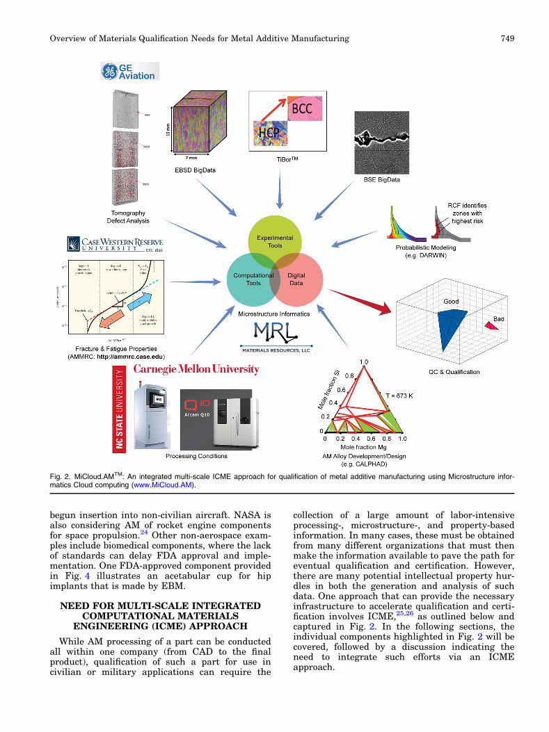
This overview proposes the use of an IntegratedComputational Materials Engineering (ICME)-based platform (MiCloud.AM) (Fig. 2), while pro-viding preliminary results to develop an under-standing of the microstructure (i.e. morphology andcrystallography), defects, and source(s) of defectgeneration. These are all influenced by processcontrol while linkages between those variables andmelt pool geometry are required to eliminate/min-imize such defects and produce desired properties.This could be accomplished by utilizing a verifiedplatform for rapid qualification of powder bed directmetal AM processes.
GLOBAL ACTIVITIES, SPECIAL JOURNALISSUES ON AM
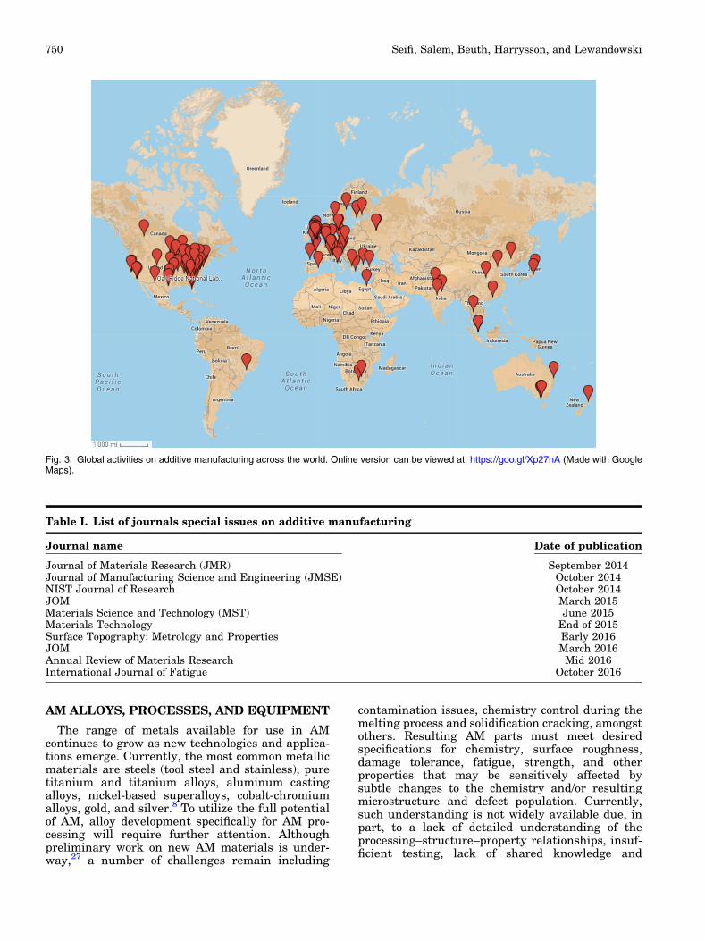
To reflect the anticipated impact of a successfulqualification methodology for AM parts, Fig. 3 illus-trates the various international R&D activities atuniversities, national laboratories and researchinstitutes as part of an ongoing review,12 whilespecific references for various European pro-grams13,14 and projects15–23 are also provided. Theurgent need for a widely used qualification processis reflected by the rapidly expanding AM R&D asillustrated in Table I which summarizes a numberof technical journals that have dedicated at leastone journal issue to the topic of AM.
INDUSTRIAL EXAMPLES OF EVOLVINGAND POTENTIAL AM APPLICATIONS
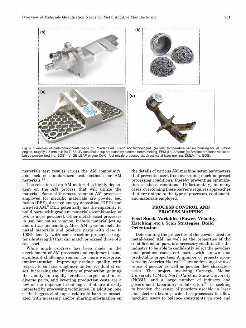
In addition to the R&D work mentioned above,there are many active investments by variousindustries for utilization of AM parts to capitalizeon the value-added properties provided by AM asshown in Fig. 4, which highlights some industrialexamples for AM parts. In particular, GeneralElectric (GE) has received Federal Aviation Admin-istration (FAA) certification for fuel nozzle imple-mentation in the GE LEAP engine, and GE Aviationwill produce more than 100,000 3D-printed partsvia laser-based powder bed AM by the close of thisdecade. In this case, AM reduced the total partcount and replaced more complex brazing of multi-ple components to create a lighter, simpler, andmore durable product. Other components are alsobeing considered for potential replacement such asbrackets. While fracture-critical components arelonger-term goals, some aerospace companies have
Fig. 1. Market share among metal powder bed fusion AM systems, (Trumpf uses directed energy deposition method). Adapted from Ref. 2.
Seifi, Salem, Beuth, Harrysson, and Lewandowski748
begun insertion into non-civilian aircraft. NASA isalso considering AM of rocket engine componentsfor space propulsion.24 Other non-aerospace exam-ples include biomedical components, where the lackof standards can delay FDA approval and imple-mentation. One FDA-approved component providedin Fig. 4 illustrates an acetabular cup for hipimplants that is made by EBM.
NEED FOR MULTI-SCALE INTEGRATEDCOMPUTATIONAL MATERIALS
ENGINEERING (ICME) APPROACH
While AM processing of a part can be conductedall within one company (from CAD to the finalproduct), qualification of such a part for use incivilian or military applications can require the
collection of a large amount of labor-intensiveprocessing-, microstructure-, and property-basedinformation. In many cases, these must be obtainedfrom many different organizations that must thenmake the information available to pave the path foreventual qualification and certification. However,there are many potential intellectual property hur-dles in both the generation and analysis of suchdata. One approach that can provide the necessaryinfrastructure to accelerate qualification and certi-fication involves ICME,25,26 as outlined below andcaptured in Fig. 2. In the following sections, theindividual components highlighted in Fig. 2 will becovered, followed by a discussion indicating theneed to integrate such efforts via an ICMEapproach.
Fig. 2. MiCloud.AMTM: An integrated multi-scale ICME approach for qualification of metal additive manufacturing using Microstructure infor-matics Cloud computing (www.MiCloud.AM).
Overview of Materials Qualification Needs for Metal Additive Manufacturing 749
AM ALLOYS, PROCESSES, AND EQUIPMENT
The range of metals available for use in AMcontinues to grow as new technologies and applica-tions emerge. Currently, the most common metallicmaterials are steels (tool steel and stainless), puretitanium and titanium alloys, aluminum castingalloys, nickel-based superalloys, cobalt-chromiumalloys, gold, and silver.8 To utilize the full potentialof AM, alloy development specifically for AM pro-cessing will require further attention. Althoughpreliminary work on new AM materials is under-way,27 a number of challenges remain including
contamination issues, chemistry control during themelting process and solidification cracking, amongstothers. Resulting AM parts must meet desiredspecifications for chemistry, surface roughness,damage tolerance, fatigue, strength, and otherproperties that may be sensitively affected bysubtle changes to the chemistry and/or resultingmicrostructure and defect population. Currently,such understanding is not widely available due, inpart, to a lack of detailed understanding of theprocessing–structure–property relationships, insuf-ficient testing, lack of shared knowledge and
Fig. 3. Global activities on additive manufacturing across the world. Online version can be viewed at: https://goo.gl/Xp27nA (Made with GoogleMaps).
Table I. List of journals special issues on additive manufacturing
Journal name Date of publication
Journal of Materials Research (JMR) September 2014Journal of Manufacturing Science and Engineering (JMSE) October 2014NIST Journal of Research October 2014JOM March 2015Materials Science and Technology (MST) June 2015Materials Technology End of 2015Surface Topography: Metrology and Properties Early 2016JOM March 2016Annual Review of Materials Research Mid 2016International Journal of Fatigue October 2016
Seifi, Salem, Beuth, Harrysson, and Lewandowski750
materials test results across the AM community,and lack of standardized test methods for AMmaterials.12
The selection of an AM material is highly depen-dent on the AM process that will utilize thematerial. Some of the most common AM processesemployed for metallic materials are powder bedfusion (PBF), directed energy deposition (DED) andwire-fed AM.8 DED potentially has the capability tobuild parts with gradient materials (combination oftwo or more powders). Other metal-based processesin use, but not as common, include material jettingand ultrasonic bonding. Most AM systems melt themetal materials and produce parts with close to100% density, with some baseline properties (e.g.,tensile strength) that can match or exceed those of acast part.8
While much progress has been made in thedevelopment of AM processes and equipment, somesignificant challenges remain for more widespreadimplementation. Improving product quality withrespect to surface roughness and/or residual stres-ses, increasing the efficiency of production, gainingthe ability to rapidly produce larger and morediverse parts, and lowering production costs are afew of the important challenges that are directlyimpacted by processing techniques. In addition, oneof the biggest challenges relates to barriers associ-ated with accessing and/or sharing information on
the details of various AM machine setup parametersthat prevents users from overriding machine-presetprocessing conditions, thereby preventing optimiza-tion of these conditions. Unfortunately, in manycases, overcoming these barriers requires approachesthat are unique to the type of processes, equipment,and materials employed.
PROCESS CONTROL ANDPROCESS MAPPING
Feed Stock, Variables (Power, Velocity,Hatching, etc.), Scan Strategies, BuildOrientation
Determining the properties of the powder used formetal-based AM, as well as the properties of thesolidified metal part, is a necessary condition for theindustry to be able to confidently select the powdersand produce consistent parts with known andpredictable properties. A number of projects spon-sored by America Makes28,29 are addressing the use/reuse of powder as well as powder flow character-istics. The project involving Carnegie MellonUniversity (CMU), North Carolina State University(NCSU), and a large number of industry andgovernment laboratory collaborators29 is seekingto broaden the range of powders useable in laserand electron beam powder bed processes to allowmachine users to balance constraints on cost and
Fig. 4. Examples of parts/components made by Powder Bed Fusion AM technologies. (a) Inlet temperature sensor housing for jet turbineengine, roughly 7.5 mm tall; (b) Ti-6Al-4V acetabular cup produced by electron beam melting, EBM (i.e. Arcam); (c) Bracket produced via laser-based powder bed (i.e. EOS); (d) GE LEAP engine Co-Cr fuel nozzle produced via direct metal laser melting, DMLM (i.e. EOS).
Overview of Materials Qualification Needs for Metal Additive Manufacturing 751

part precision through their choice of powder sys-tems. That project has recently demonstrated thesuccessful use of two nonstandard Ti-6Al-4V powdersystems in the Arcam machine through processvariable changes.
Ongoing work at CMU/Wright State University(WSU) as part of the existing project on RapidQualification Methods (America Makes contract No.FA8650-12-2-7230 and Project No. 4009) led by CaseWestern Reserve University (CWRU) and CMU is
Fig. 5. (a) P–V map for electron beam processed Ti-6Al-4V showing regimes of good quality beads as well as size of beta grains.35 (b) Insetshows different scales of surface roughness of multi-layer beads produced via laser-based techniques at different P–V combinations.
Fig. 6. Regimes of P and V in typical AM processes.
Seifi, Salem, Beuth, Harrysson, and Lewandowski752

directly developing Process Mapping strategies30–35
where beam power and velocity (i.e. P–V) are variedthrough a series of experiments (single bead onplate, single layer pads, multi-layer pads, compo-nents and component features). Those experimentsare combined with finite element thermal modelingof the melt pool geometry to define regimes of goodquality deposits (e.g., avoiding lack of fusion, avoid-ing keyholing,36 increasing build rate, increasingprocess precision) across wide ranges of processvariables. Figure 5 shows a recently developed P–Vmap35 for Ti-6Al-4V produced for electron beam (i.e.Arcam) single bead or raster deposits, while laser-based (i.e. EOS) deposits of Ti-6Al-4V, IN718,IN625, AlSi10Mg, CoCrMo, maraging steel andstainless steel are also in the various stages ofbeing mapped. Maps of these powder fusion exper-iments are being correlated with surface rough-ness37 and mechanical property measurements11,12
being performed at CWRU. In addition to changes tothe bead quality shown in Fig. 5, changes to thesurface roughness are also evident in differentregimes of P–V space.37 Surface roughness of as-deposited surfaces and/or internal passages may beparticularly important for HCF and/or fluid flowapplications.
In addition, mapping process outcomes acrossIN625, IN718, stainless steel, Al-Si-10Mg and cobaltchrome alloys are being conducted at CMU (e.g.Ref. 34). The full range of beam powers and travelspeeds in typical AM processes (Fig. 6), is also beingaddressed.31 Building on earlier work,38,39 processmapping is also being applied to the feedforwardand feedback control of microstructure in AMprocesses through the mapping of thermal condi-tions (e.g. cooling rates) at key temperatures acrossprocess variable space. Figure 7 gives an example40
of feedforward capability, where Ti-6Al-4V betasolidification microstructure (beta grain width) iscontrolled across three specimens through prede-termined changes in process variables to yield grainwidths that are roughly twice and three times thesmallest grain width value of 91 lm. Where thisfigure demonstrates control of microstructure size
across different specimens, recent results havedemonstrated the feedforward control of microstruc-ture size with location within single specimens.
IN SITU PROCESS MONITORING ANDFEEDBACK CONTROL
In situ process monitoring and control are one ofthe key evolving areas that could impact qualifica-tion and certification of parts where qualitydemands are extremely high, such as aerospaceand medical devices. The ability to produce multipleparts consistently across machines, operators, andmanufacturing facilities could require the integra-tion of various process monitoring and measure-ment tools. While careful and consistent processcontrol can limit variability, the lack of adequateprocess measurement methods hinders more wide-spread use of the technology. Currently, processcontrol based on heuristics and experimental datahas only yielded limited improvements in partquality. As documented in a recent NIST report,traceable dimensional and thermal metrology meth-ods must be developed for real-time closed-loopcontrol of AM processes.41
Variability in AM machines and/or beamsource/material interactions can create inconsis-tency in the microstructure, presence of defects,and variability in the mechanical performance.While in situ monitoring has been used in the pastfor DED, its use in the PBF processes is challengingdue to limited access to the melt pool to enableimaging which is further complicated by the higherprocess velocity (Fig. 6). Recent attempts on processmonitoring of PBF focused on defect detection andmelt pool characterization that can be interrogatedin situ. Melt pool monitoring is being used tocapture the distribution of temperature withindeposited layers in order to generate a heat mapthat can be compared to melt pool size.42,43 How-ever, high bandwidth data acquisition (e.g. 1000 s ofHz) and processing can generate enormous datasetsthat are difficult to manage while also requiringenormous amounts of data storage (e.g., 1000 s of
Fig. 7. Feedforward control of Ti-6Al-4V solidification microstructure in the Arcam process, varying beta grain width over a factor of 3.
Overview of Materials Qualification Needs for Metal Additive Manufacturing 753

GB). Nonetheless, various machine OEMs havebegun to deploy process monitoring options for theirequipment. One example, Concept LaserTM, pro-vides a quality assurance monitoring system (e.g.,QMmeltpool 3D) that intends to detect processingdefects at early stages, thereby providing a meansfor process optimization.42 In the next generation ofmachines under development, one of the desires isthe retention of x–y location information for all datathroughout the build, thereby permitting the gen-eration of a high-resolution 3D rendering of sensorsignals. Ultimately, this may provide a qualityassurance diagnostic similar to non-destructivetesting (NDT) akin to computed tomography. Com-parable systems are also being provided by othervendors such as ArcamTM (LayerQam), SLM Solu-tionsTM, and EOSTM. As indicated in recentreviews,41 while process monitoring is necessaryand has received significant interest, this technol-ogy for PBF is still in its infancy.
In the research community, feedback controlapproaches are being pursued at CMU in collabo-ration with significant efforts on process sensing.For the LENS process, indirect control ofmicrostructure through thermal imaging and con-trol of the melt pool is being pursued with PennState and Stratonics through the linking of observ-able melt pool dimensions to the formation ofmicrostructural features. Thermal control of theArcam process is being implemented through ther-mal imaging of the entire build after layers arefused via an infrared system installed at theUniversity of Texas at El Paso. CMU-developedprocess maps are being used to prescribe in-processchanges in beam power and/or beam velocity tocompensate for changes in average temperature inthe build, yielding consistent microstructure sizeswith part height. LLNL44 is also leading variousmodeling and simulation activities including meltpool monitoring.
MICROSTRUCTURE AND DEFECTCHARACTERIZATION/QUANTIFICATION
The performance of an AM part is directlyaffected by the underlying microstructure that is apermanent record of the processing pedigree. Whilethe process mapping studies outlined above for Ti-6Al-4V appear to be successful in mapping coarsemicrostructural features during solidification (e.g.,beta grain size), additional emphasis is needed onsolid state phase transformations that occur duringsubsequent cooling to room temperature as well asany thermal transients that occur during the build.The flexibility of producing complicated geometriesby AM will require the ability to change location-specific processing parameters to optimize thepowder melting and solidification rates towardsproducing parts free of defects and with desiredmicrostructural features over a range of size andlength scales. Microstructure heterogeneity (mor-phology, crystallography, and alignment withbuild direction) is expected and perhaps desiredin some cases. While location-specific microstruc-ture heterogeneities are to be expected/desired inparts with complicated geometries due to geometri-cal heterogeneities, location-specific microstructurevariability11 has been reported in geometricallyhomogeneous primitive shapes (e.g., cuboids). Whiledefects (e.g., lack of fusion, voids) detected inprevious work11 and shown in Fig. 8 are mainconstituents of the microstructure, they will bediscussed in a separate section due to the differentmethodology of characterization (i.e. lCT scans) aswell as the need to link them to probabilisticapproaches for fracture, fatigue, and lifingpredictions.
Various works have shown that electron beamAM of Ti-6Al-4V parts with a preheated powder bedproduce solidification rates and beta grain sizesconsistent with that shown in Figs. 5 and 7,
Fig. 8. Examples of lack of fusion: (a) metallographic cross-section, (b) fracture surface of as-deposited EBM Ti-6Al-4V tested in fatigue tofailure. Defects shown present perpendicular to the build orientation in both cases.
Seifi, Salem, Beuth, Harrysson, and Lewandowski754

depending on the P–V combinations employed.However, the finer scale microstructural featurespost-solidification also depend on cooling rate aswell as any thermal transients that occur duringmulti-layer deposition that may produce a
basketweave microstructure with alpha-lath thick-nesses less than 1 lm. In contrast, laser-basedtechniques without preheated powder beds producemore rapid solidification and cooling rates in thesolid state, along with the observation of
Fig. 9. (a) Build direction IPF maps for the alpha phase (right) and reconstructed beta phase (left) in the bottom, mid-height and top of the EBM-deposited Ti-6Al-4V SL sample;11 (b) comparison between texture from large area EBSD scans (left) and small area EBSD scans (right) showingthe strong texture in the small area scans.
Overview of Materials Qualification Needs for Metal Additive Manufacturing 755
martensitic microstructures37 in the as-depositedcondition. In the case of electron beam AM process-ing where the solidification/cooling rates are some-what slower, the alpha laths (hcp) are produced viaphase transformation of prior beta (bcc) upon cool-ing below the beta transus (�1000�C), while themorphology and crystallography of the prior betagrains are dependent on the cooling rate and builddirection.38,45 As such, electron backscatter diffrac-tion (EBSD) techniques are often used first tocapture the crystallography and morphology of theroom temperature alpha phase, followed by recon-struction of the prior beta phase using the Burgerorientation relationship between alpha and beta,46
as explained below.
LARGE AREA BSE/EBSD, MACRO/MICROTEXTURE EVOLUTION
Practical microstructure characterization requiresdesigning the inspection volume to be large enoughto capture relevant statistics about the feature ofinterest (FOI)45 at a high enough resolution for thelowest possible cost (i.e. least recording time). In AMparts made of Ti-6Al-4V by electron beam tech-niques, one of the major FOI is the high-temperaturebeta grain size. However, the beta phase has a smallvolume fraction at room temperature,45 whichmakes it difficult/expensive to record using EBSD.Alternatively, the alpha phase is recorded at roomtemperature, and the beta phase is then recon-structed from the alpha phase using the Burgerorientation relationship [TiBor @ www.MiCloud.AM], although the inspection volume must beselected carefully as demonstrated below.
Figure 9a shows build direction inverse polefigure (IPF) maps for alpha phase (right) andreconstructed beta phase (left) for an as-depositedtall build (i.e. 100 mm) of EBM Ti-6Al-4V, usingEBSD data collected from 500 lm 9 500 lm areas.Analyses of the data from this scan area did notreveal obvious variation in the alpha phasemicrostructure between the start (i.e. bottom) ofthe build and the end (i.e. top) of the build shown inFig. 9a. However, the IPF maps of the reconstructedbeta revealed some differences between the startand end of the build, highlighting the importance ofinspecting the microstructure of beta phase afterAM. Further inspection of the beta reconstruction inFig. 9a (left) also shows that only a limited numberof beta grains (e.g.,<5) have been captured withinthis scan area, which does not result in reliablestatistics to link processing-microstructure, andperformance for qualification purposes.
In order to address this and illustrate the impor-tance of scan area, our EBSD data generation hasbeen designed to satisfy two conditions: (1) highenough resolution to record alpha orientations fromthin laths and (2) covering an area that is largeenough to record data from many prior beta grainsfor reliable statistics, recognizing that each betagrain can be multiple millimeters in size dependingon the AM process and P–V conditions employed.While many modern scanning electron microscopescan record EBSD scans from large areas (e.g.,5 mm 9 5 mm) at high resolution (e.g., 1 lm stepsize), analyzing large files (e.g. 25,000,000 alphaorientations) is a challenge for many commercialsoftware running on standalone PCs. To address
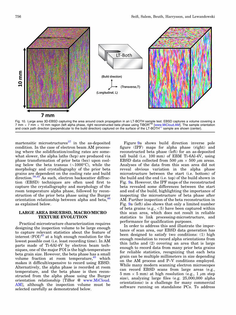
Fig. 10. Large area 3D-EBSD capturing the area around crack propagation in an LT-BOTH sample test. EBSD captures a volume covering a7 mm 9 7 mm 9 10 mm region (left alpha phase, right reconstructed beta phase using TiBORTM [www.MiCloud.AM]. The sample orientationand crack path direction (perpendicular to the build direction) captured on the surface of the LT-BOTH11 sample are shown (center).
Seifi, Salem, Beuth, Harrysson, and Lewandowski756

this challenge, many tools were developed withinMiCloud.AM to conduct data analytics on Big EBSDdatasets (as large as 100,000,000 orientations cov-ering 10 mm 9 10 mm areas at 1 lm resolution)using various data mining techniques and cloudcomputing.
Figure 9a and b clearly shows that both themorphology of the prior beta and texture of thealpha phase are unreliably presented in commonlyused 500 lm 9 500 lm EBSD scans for AM Ti-6Al-4V parts, in contrast to the large EBSD scans shownin Fig. 9b. In particular, analyses of the polefigures of the alpha phase obtained from a500 lm 9 500 lm region showed much sharpertexture intensity (�13–21 times random) than hasbeen recorded by 150,000 lm 9 10,000 lm scans(�2 times random) (Fig. 9b). In addition, the loca-tions of various texture components were drasticallydifferent.
Large area scans may be particularly relevant forcorrelating fracture paths in AM samples/parts aswell as the orientation dependence of microstruc-ture and fracture properties between different buildorientations. This is first demonstrated by compar-ing the tall build in Fig. 9a to a different buildorientation shown in Fig. 10 where large EBSDscans were similarly conducted to produce the 3Dimages of the as-deposited material in Fig. 10. The
reconstructed beta grains in Fig. 10 (right) areconsistent with those shown along the build direc-tion in Fig. 9a (right). Figure 10 was constructedfrom an as-deposited sample that was fracturetested in the LT-BOTH orientation11 shown, and acrack was captured in the regions analyzed. It isworth noting that the alpha texture around thecrack from a 7 mm 9 7 mm scan area was only �1.6times random (Fig. 11 (top right)) in contrast to thatshown for the 250-lm scan area shown in Fig. 11(bottom right), in agreement with the findingsshown earlier in Fig. 9 even with the 90� differencein the build direction. These preliminary observa-tions reveal the importance of conducting large areaEBSD scans for accurate qualification based onlinking processing-microstructure-performance inTi-6Al-4V AM parts, as well as correlatingmicrostructure features to the fracture path, asdiscussed below.
MECHANICAL PROPERTY MEASUREMENTS(FRACTURE/FATIGUE)
One of the key aspects for qualification of AMparts/components is the mechanical performancethat requires a wide range of mechanical testing/characterization. Measurement science for the AMindustry to determine material properties in a
Fig. 11. Top surface of 3D-EBSD image shown in Fig. 10 that captures the crack growth in an LT-BOTH11 sample. Build direction IPF map foralpha phase (left) and the associated 0001 pole figure for the whole scan (right top) and a single 250 lm 9 250 lm tile shown at top left, (0001)pole figure at right bottom, where the build direction is parallel to the pole figure normal direction. It is necessary, due to the coarseness of themicrostructure, to capture data over a large area in order to accurately represent the total texture.
Overview of Materials Qualification Needs for Metal Additive Manufacturing 757
standardized way has gathered a significantamount of interest over the last 3 years.41,47,48
Currently, there are no consensus-based publicstandards in this area, except for a few examplesrelated to terminology and data file formats.49,50
The ASTM International Committee F42 on Addi-tive Manufacturing Technologies and the Interna-tional Organization for Standardization (ISO)TC261 Committee on Additive Manufacturing havestarted separately, and in some cases jointly, stan-dard development to address this deficiency.
Most recently, America Makes co-sponsored anevent51 to help coordinate U.S. standards develop-ment activities for AM. Key standards developingorganizations (SDOs), including ASTM, SAE,ASME, SME, AWS, etc., along with a number ofOEMs, gathered to discuss and facilitate collabora-tive efforts with the goal of initiating a dialogue onjoint standards development for AM. These activi-ties are being viewed as one mechanism that canfacilitate product qualification and certification. Forexample, aero engine parts could be certified byFAA while biomedical parts could be certified byFDA. The overarching goal of these coordinationefforts is to produce a roadmap that will minimizethe amount of overlap activities across the variousstandardization organizations.
Static properties (e.g., YS, UTS, etc.) can bemeasured using already developed standards thatare being modified to accommodate the uniqueorientations and aspects provided by AM process-ing.50,52 However, when fracture-critical propertiesare a concern, utilizing conventional methods andstandards may produce some challenges anduncertainty,53 particularly with regard to mea-suring location-specific fracture properties. Exam-ples are the measurement of fracture toughness,fatigue crack growth and high cycle fatigue
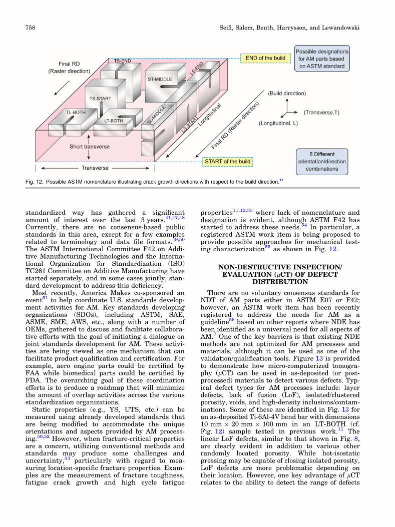
properties11,12,35 where lack of nomenclature anddesignation is evident, although ASTM F42 hasstarted to address these needs.54 In particular, aregistered ASTM work item is being proposed toprovide possible approaches for mechanical test-ing characterization55 as shown in Fig. 12.
NON-DESTRUCTIVE INSPECTION/EVALUATION (lCT) OF DEFECT
DISTRIBUTION
There are no voluntary consensus standards forNDT of AM parts either in ASTM E07 or F42;however, an ASTM work item has been recentlyregistered to address the needs for AM as aguideline56 based on other reports where NDE hasbeen identified as a universal need for all aspects ofAM.7 One of the key barriers is that existing NDEmethods are not optimized for AM processes andmaterials, although it can be used as one of thevalidation/qualification tools. Figure 13 is providedto demonstrate how micro-computerized tomogra-phy (lCT) can be used in as-deposited (or post-processed) materials to detect various defects. Typ-ical defect types for AM processes include: layerdefects, lack of fusion (LoF), isolated/clusteredporosity, voids, and high-density inclusions/contam-inations. Some of these are identified in Fig. 13 foran as-deposited Ti-6Al-4V bend bar with dimensions10 mm 9 20 mm 9 100 mm in an LT-BOTH (cf.Fig. 12) sample tested in previous work.11 Thelinear LoF defects, similar to that shown in Fig. 8,are clearly evident in addition to various otherrandomly located porosity. While hot-isostaticpressing may be capable of closing isolated porosity,LoF defects are more problematic depending ontheir location. However, one key advantage of lCTrelates to the ability to detect the range of defects
Fig. 12. Possible ASTM nomenclature illustrating crack growth directions with respect to the build direction.11
Seifi, Salem, Beuth, Harrysson, and Lewandowski758

indicated as well as their location while alsoenabling the confirmation of the effectiveness ofpost-processing treatments.
MICROSTRUCTURAL/MECHANICAL/DEFECT INTERACTION OR COMPETITION
Figure 14 is provided to highlight the recentobservations11,12,35 of location-dependent propertiesin as-deposited Ti-6Al-4V produced by electronbeam powder bed processing in the context of thepresent overview. Fracture toughness experimentsconducted in three different locations on a tallbuild (i.e. 20 mm 9 10 mm 9 100 mm) revealedsignificant differences. Ongoing work57–59 is char-acterizing the defect density and type as well asmicrostructural features using some of the tech-niques outlined in this overview. Fracture-criticalproperties are affected by a variety of factors andtwo of the dominant factors are defect density andmicrostructure variation. Some properties (e.g.,
HCF, toughness) are very sensitive to defects asthese provide potent fracture nucleation sites12,60
as well as preferred regions for crack growth whileother dominant factors include microstructuralfeatures at a range of size and length scalesdepending on the property of interest.61 In theexample shown in Fig. 14, while a lower defectdensity was present toward the end of the build inthe region of high toughness, microstructuraldetails were also different from the start to theend of the build (e.g., Fig. 9) thereby preventing adirect correlation. This highlights the continuingneed for a comprehensive examination of variousfactors (e.g., defects, microstructure, residualstress, etc.) controlling the mechanical behavior ofAM materials while also integrating modeling andexperimentation efforts to produce materials/partswith desired location-specific properties.35,58,59 Thisemphasizes the need of an ICME approach forqualification.
Fig. 13. Computed tomography image of as-deposited and subsequently fractured Ti-6Al-4V sample with dimensions10 mm 9 20 mm 9 100 mm. Crack growth is in the LT-BOTH orientation.11 Planar lack of fusion defects and random porosity is evident atvarious locations. Lack of fusion defects detected are of similar size to that shown in Fig. 8 and reported previously.11 Resolution limit for thisscan was 10–20 lm. Finer resolution is possible with smaller sample size/volume.
Overview of Materials Qualification Needs for Metal Additive Manufacturing 759

PROBABILISTIC MODELING OF FRACTUREAND FATIGUE
While the goal of producing defect-free parts inas-deposited materials remains an area of extremeinterest, inspection processes (e.g., x-ray tomogra-phy, UT, acoustics, etc.) and various post-processingtechniques (e.g., HIP, heat treatment, etc.) maycontinue to need to be implemented for use infracture-critical applications. However, non-criticallocations (i.e. low stress, strain) in fracture criticalparts may not require the same damage tolerance/properties required in highly stressed areas (Fig. 2).There has been increased use of probabilistic meth-ods for design assessment of reliability with inspec-tion (DARWIN)62 for a variety of processingtechniques (e.g., casting, forging, heat treatment,etc.) to deal with local variations in microstructure/defects/properties in lifing estimates. Programssuch as DARWIN and others have been shown toreduce significantly computation time compared to
other methods (e.g., Monte Carlo). In addition,proper sampling strategies can be employed toachieve a desired sampling accuracy result for agiven confidence interval, thereby focusing on vari-ables that should have the most effect on riskreduction.62 While probabilistic approaches havebeen used successfully in previous work for predict-ing thresholds for cracking in commercial alu-minum alloys,63,64 such approaches would alsoappear to be useful for modeling/predicting theeffects of changes in AM process variables onsubsequent performance as well as modeling loca-tion-specific properties.
MICROSTRUCTURE INFORMATICS,MODELING AND SIMULATION—AN ICME
APPROACH
Due to the complicated nature of the AM process,a coherent integration between various stages andscales of modeling the materials behavior and the
Fig. 14. Location-dependent properties in as-deposited EBM Ti-6Al-4V materials are affected by convoluted interactions between defect-dominated and microstructure-dominated contributions.
Seifi, Salem, Beuth, Harrysson, and Lewandowski760
corresponding measurements is critically neededwithin the framework of the Materials GenomeInitiative (MGI)65–67 and ICME.25,26,68–74 In partic-ular, AM will benefit from the ICME goal ofenabling optimization of materials, manufacturingprocesses, and component design long before com-ponents are fabricated by integrating computationalprocesses involved into a holistic system. Develop-ing and implementing such a system will enable amore efficient qualification process using big datascience approaches.71,72
As a demonstration of the practical implementa-tion of an ICME approach, the team involved in thiseffort integrated efforts from academia, OEMs, anda small business all working on various projectswith different funding sources. However, all mem-bers recognized the value of collaboration andintegration of results obtained using various tools.To enhance such a collaboration and integration ofefforts, three major elements were identified: (1) apart that could be produced, (2) datasets to becollected, and (3) a platform to consolidate all thedata for analysis using state of the art data-miningalgorithms. In addition, an efficient workflow45 isneeded to promote transparency and efficient col-laborations between materials experts and manu-facturing/design specialists by providing anunderstanding of the various mesoscale hetero-geneities that develop naturally in the workpieceas a direct consequence of the inherent heterogene-ity imposed by the AM process.
While each team member was responsible for oneor more of the items above, the communication wasled by CWRU under various non-disclosure agree-ments that allowed the exchange of informationwhile respecting the Intellectual property (IP) ofeach team member. To avoid any issues withproprietary designs, the team also selected todemonstrate such collaboration on rectangularcoupons. Each team member maintained the detailsof characterization procedures while sharing theinputs and outputs for each process with the team.The shared data were provided in standard formatsthat are common in the public domain, such asASCII files and images. A practical implementationof such a workflow has been deployed at www.MiCloud.AM as the first microstructure-based AMsoftware-as-a-service (SaaS). It is designed on threemain pillars: (1) data science protocols for efficientanalysis of large datasets, (2) protocols for extract-ing reduced descriptions of salient microstructurefeatures for insertion into simulations (e.g., regionsof homogeneity), and (3) protocols for direct andefficient linking of materials models/databases intoprocess/performance simulation codes45 (see Fig. 2).
In the initial phases of this collaboration, datagenerated/provided to CWRU were then importedto MiCloud.AM for data mining. The results ofmicrostructure informatics and data mining (i.e.data products) were then shared with the restof the team towards establishing correlations for
qualification. Such a data flow is made possible viausing MiCloud.AM with multiple functionalitiesincluding Big Data storage, analytics, and visual-ization capabilities.
Development of accurate AM modeling and sim-ulation tools is an important fundamental buildingblock for an ICME approach for AM. The availabil-ity of good validated physics-based modeling andsimulation tools decreases the need for experimen-tal testing of technologies and processes and givesproduct designers a predictive capability to optimizepart designs. Accurate models are also vital fordeveloping the required control technologies andsoftware for AM, developing standards, and estab-lishing qualification/certification procedures.
The accuracy of predictions using various simula-tion tools is heavily dependent on the availability ofcomprehensive data on materials and depositionprocessing for calibration, validation, and verificationprocesses. While there have been many recentattempts to develop such models,75 the complicatednature of the AM process affect the current accuracyof predictions for developing comprehensive simula-tion-based qualification tools. Furthermore, toincrease the accuracy of predictions, these toolsrequire a better understanding of the fundamentalprocesses and physical phenomena that underlie AMfeedstock inputs, approaches, and technologies whichare not possible without generating and analyzing alarge amount of data and sharing them amongmultiple collaborating companies as described herein.
QUALIFICATION/CERTIFICATIONPATHWAY
Statistically-based legacy qualification processesfor metallic materials require extensive testing thatmay cost millions of dollars and take up to 15 yearsto complete.76 This approach is not practical forqualifying AM parts that are known for drasticvariability in processes and processing parameterswithin each process. On the other hand, model-based qualification requires a smaller number oftests to validate the model. However, the rapid andcomplicated AM process adds many challenges todeveloping physics-based models with repeatabilityand reproducibility of predictions across varyingprocesses and process parameters. The proprietarynature of process controls that are imposed bycommercial machine manufacturers drasticallyreduces the availability of data needed to calibrateand validate models that are necessary for themodel-based qualification.
Recently, Dave Abbott of GE77 demonstrated thesuccess of GE in certifying the GE9X T25 Sensorand the LEAP Fuel Nozzle without the need for newqualification standards. While this approach is verypromising and an excellent example for parts thatare produced in mass production, it will be crucial toestablishing its implementation on small(er)batches of other AM parts.
Overview of Materials Qualification Needs for Metal Additive Manufacturing 761
In the realm of components or repairs producedby direct deposition of Ti-6Al-4V, AMS standard4999A78 prescribes certain conditions for feedstockcomposition, atmosphere, and post-processing (i.e.HIP and/or heat-treatment) to be used in produc-tion, as well as minimum standards for tensile andfracture toughness properties in finished productsand standardized acceptance testing procedures foreach production run (consisting of composition,mechanical properties along and perpendicular tothe build direction, microstructure and surfacecontamination, and NDT by ultrasound and radio-graphy) along with re-test and rejection criteria.The standard also provides for a qualificationpathway consisting of several stages: (1) sourcequalification, including>50 tensile test results fromeach principal build direction (i.e. X, Y, Z) covering 3different configurations and 3 different feedstockheats and meeting specified property and variationlimits; (2) approval of deposition or deposition/ge-ometry parameters, with sufficient tensile andstrain-controlled fatigue test coupons produced tocover the space of processing and geometricalparameters in the component, including depositionpower and feed rate, feedstock, deposit height,width, and length, inclination angle, scan strategy,intersection angle and orientation, etc.; and (3)production qualification by destructive testing ofone or more production-level parts by >12 tensiletests in each direction. Upon qualification, each ofthe production parameters is fixed, with any devi-ations requiring additional testing.
The qualification procedure prescribed inAMS4999A is a classic example of statistically-based qualification, wherein the uncertainty in theproduction of a particular component is understoodand mitigated by massive upfront testing, followedby ongoing quality control testing during produc-tion. It is very similar to the procedure that has longbeen used for aerospace castings,79 where any otherthan very minor deviation from the qualified proce-dure triggers a re-qualification process. While sucha procedure is suitable for serial production ofnumerous identical parts (such as the fuel nozzlementioned above), it represents a high barrier forproduction of customized, repair, and low-volumecomponents where AM techniques are often mostdesirable, and demonstrates a clear need for holis-tic, ICME-based qualification schemes that encom-pass pre-process, in-process, and post-process datato facilitate demonstration of part suitability accord-ing to a ‘‘qualify as you go’’ paradigm.80
SUMMARY AND FUTURE TRENDS
This article is provided as an attempt to capturean overview of the various challenges to be consid-ered in the qualification of metal AM. These includethe need for various modeling and experimentalactivities, along with the integration of such effortsat the size and length scales relevant for intended
applications. In addition, a proposed example ofmulti-organization collaboration towards address-ing some of the qualification challenges was demon-strated via an implementation of an ICME approachvia BigData analytics and cloud computing.
ACKNOWLEDGEMENTS
This work was partly supported by AmericaMakes, the National Additive Manufacturing Inno-vation Institute, under Project No. 4009: ‘‘RapidQualification Methods for Powder Bed Direct MetalAdditive Manufacturing Processes’’ through Con-tract No. FA8650-12-2-7230 and it is highly appre-ciated. Additional support was provided by twoASTM International Scholarship Awards (M. Seifi)and the Armington Professorship (J. J. Le-wandowski). Various discussions with academicteam members as well as industrial partners andgovernment laboratories during monthly webinarsare appreciated. These include four other universitypartners (NCSU, CMU, U of L, and WSU), fiveindustrial partners (Lockheed Martin, Pratt &Whitney, GE, Kennametal, and Bayer) and twogovernment laboratories (ORNL and NIST). M. Seifiappreciates various discussions with ASTM F42/E08/E07 committee members. A. Salem and EBSDwork are supported under a NAVAIR SBIR ‘‘Adap-tive Microstructure-Based Approach for RapidQualification by Similarity of Ti-6Al-4V PartsManufactured by Additive Manufacturing (AM)Techniques’’ under Contract No. N6833515C0209.The help of Dr. Daniel Satko of MRL in generatinglarge-scale EBSD data is appreciated. The tomog-raphy analysis shown in Fig. 13 was conducted byMs. Whitney Yetter at GE Inspection Technologieswhile the tomography analysis shown in Fig. 14 wasconducted by Mr. Daniel Rankin at YXLON, adivision of COMET Technologies, Inc.
REFERENCES
1. ASTM Standard F2792, ASTM Book of Standards (WestConshohocken: ASTM International, 2012).
2. T. Caffrey and T. Wohlers, Wohlers Report-3D printing andAdditive Manufacturing State of Industry (2015).
3. C.L. Weber, V. Pena, M.K. Micali, E. Yglesias, S.A. Rood,J.A. Scott, and B. Lal, Inst. Def. Anal. 6 (2013).
4. D.L. Bourell, M.C. Leu, and D.W. Rosen, Roadmap forAdditive Manufacturing: Identifying the Future of FreeformProcessing (2009).
5. C.B. Williams, T.W. Simpson, and M. Hripko, NIST Tech-nical Note 1823—Additive Manufacturing Technical Work-shop Summary Report (2013).
6. Energetics Incorporated, Measurement Science Roadmapfor Metal-Based Additive Manufacturing—Workshop Sum-mary Report (2013).
7. J.M. Waller, B.H. Parker, K.L. Hodges, E.R. Burke, J.L.Walker, and E.R. Generazio, Nondestructive Evaluation ofAdditive Manufacturing State-of-the-Discipline Report,(2014).
8. W.E. Frazier, J. Mater. Eng. Perform. 23, 1917 (2014).9. W.E. Frazier, D. Polakovics, and W. Koegel, JOM 53, 16
(2001).10. W. Frazier, Solid Free Form Fabr. Proc. 717 (2010).11. M. Seifi, M. Dahar, R. Aman, O. Harrysson, J. Beuth, and
J.J. Lewandowski, JOM 67, 597 (2015).
Seifi, Salem, Beuth, Harrysson, and Lewandowski762

12. J.J. Lewandowski and M. Seifi, Annu. Rev. Mater. Res. 46(2016).
13. Directorate-General for Research and Innovation, Horizon2020 in Brief—The Framework Programme for Researchand Innovation (2014).
14. Materials Science and Engineering Expert Committee(MatSEEC), Metallurgy Europe—A Renaissance Pro-gramme for 2012–2022 (2012).
15. RepAIR—Future RepAIR and Maintenance for Aerospaceindustry. [Online]. http://www.rep-air.eu/. Accessed 15 Sep2015.
16. Reinforcing Additive Manufacturing Research CooperationBetween CMRDI and the European Research Area. [On-line]. http://www.fp7-admera.org/. Accessed 15 Sep 2015.
17. AMAZE: Additive Manufacturing Aiming Towards ZeroWaste & Efficient Production of High-Tech Metal Products.[Online]. http://www.amaze-project.eu/. Accessed 15 Sep2015.
18. AMCOR: Additive Manufacturing for Wear and CorrosionApplications. [Online]. http://www.amcor-project.eu/. Ac-cessed 15 Sep 2015.
19. The European collaboration on Additive Manufacturing.[Online]. http://www.rm-platform.com/. Accessed 15 Sep2015.
20. ManSYS: MANufacturing and supply chain managementSYStem for Additive Manufacturing. [Online]. http://www.mansys.info/. Accessed 15 Sep 2015.
21. Industrial and Regional Valorization of FoF Additive Man-ufacturing Projects. [Online]. http://www.fofamproject.eu/.Accessed 15 Sep 2015.
22. Support Action for Standardisation in Additive Manufac-turing. [Online]. http://www.sasam.eu/. Accessed 15 Sep2015.
23. Development of Aero Engine Component Manufacture usingLaser Additive Manufacturing. [Online]. http://www.merlin-project.eu/. Accessed 15 Sep 2015.
24. S. Draper, I. Locci, B. Lerch, D. Ellis, P. Senick, M. Meyer, J.Free, K. Cooper, and Z. Jones, 66th International Astro-nautical Congress (2015), pp. 1–9.
25. J. Allison, B. Cowles, J. DeLoach, T. Pollock, and G. Spanos,Integrated Computational Materials Engineering (ICME):Implementing ICME in the Aerospace, Automotive, andMaritime Industries (The Minerals, Metals & MaterialsSociety, 2013).
26. Integrated Computational Materials Engineering: ATransformational Discipline for Improved Competitivenessand National Security (The National Academies Press,2008).
27. P.C. Collins, R. Banerjee, S. Banerjee, and H.L. Fraser,Mater. Sci. Eng., A 352, 118 (2003).
28. America Makes Project 4049, Economic Production of NextGeneration Orthopedic Materials Through Powder Reuse inAM (2015). [Online]. https://americamakes.us/home-2/item/771-economic-production-of-next-generation-orthopedic-materials-through-powder-reuse-in-am. Accessed 15 Sep 2015.
29. America Makes Project 4028, A Database Relating PowderProperties to Process Outcomes for Direct Metal AM, (2015).[Online]. https://www.americamakes.us/home-2/item/500-a-database-relating-powder-properties-to-process-outcomes-for-direct-metal-am. Accessed 15 Sep 2015.
30. J. Gockel, J. Beuth, and K. Taminger, Addit. Manuf. 1–4,119 (2014).
31. J. Beuth, J. Fox, J. Gockel, C. Montgomery, R. Yang, H.Qiao, P. Reeseewatt, A. Anvari, S. Narra, and N. Klingbeil,Solid Freeform Fabrication Proceedings (2013), pp. 655–665.
32. J. Gockel and J. Beuth, Solid Freeform Fabrication Pro-ceedings (2013), pp. 666–674.
33. E. Soylemez, J.L. Beuth, and K. Taminger, Proceedings of2010 Solid Freeform Fabrication Symposium (August,2010), pp. 571–582.
34. C. Montgomery, J. Beuth, L. Sheridan, and N. Klingbeil,Proceedings of Solid Freeform Fabrication Symposium(2015), pp. 1195–1204.
35. M. Seifi, D. Christiansen, J.L. Beuth, O. Harrysson, and J.J.Lewandowski, Ti-2015: The 13th World Conference onTitanium (Wiley, 2016).
36. W.E. King, H.D. Barth, V.M. Castillo, G.F. Gallegos, J.W.Gibbs, D.E. Hahn, C. Kamath, and A.M. Rubenchik, J.Mater. Process. Technol. 214, 2915 (2014).
37. D. Christensen, M. Dahar, J. Beuth, and J.J. Lewandowski,Unpublished results (2015).
38. P. A. Kobryn and S. L. Semiatin, JOM, 40 (2001).39. S. Bontha, The Effect of Process Variables on Microstructure
in Laser-Deposited Materials (Dayton: Write State Univer-sity, 2006).
40. S.P. Narra, R. Cunningham, D. Christiansen, J. Beuth, andA.D. Rollett, Proceedings of Solid Freeform FabricationSymposium (2015), pp. 626–635.
41. M. Mahesh, B. Lane, A. Donmez, S. Feng, S. Moylan, and R.Fesperman, NISTIR 8036—Measurement Science Needs forReal-time Control of Additive Manufacturing Powder BedFusion Processes (SAE International, 2015).
42. Concept Laser’s QMmeltpool 3D: In-situ quality assurancewith real-time monitoring down to the micron level, vol. 1,no. 2 (Inovar Communications Ltd, 2015), pp. 69–71.
43. S.S. Babu, L. Love, R. Dehoff, W. Peter, T.R. Watkins, and S.Pannala, MRS Bull. 40, 1154 (2015).
44. W. King, A.T. Anderson, R.M. Ferencz, N.E. Hodge, C. Ka-math, and S.A. Khairallah, Mater. Sci. Technol. 31, 957(2015).
45. A.A. Salem, J.B. Shaffer, D.P. Satko, S. Semiatin, and S.R.Kalidindi, Integr. Mater. Manuf. Innov. 3, 24 (2014).
46. G.A. Sargent, K.T. Kinsel, A.L. Pilchak, A.A. Salem, andS.L. Semiatin, Metall. Mater. Trans. A 43, 3570 (2012).
47. J. Slotwinski and S. Moylan, NISTIR 8005—Applicability ofExisting Materials Testing Standards for Additive Manu-facturing Materials (2014).
48. J. Slotwinski, A. Cooke, and S. Moylan, NISTIR7847—Mechanical Properties Testing for Metal Parts Madevia Additive Manufacturing: A Review of the State of the Artof Mechanical Property Testing (2012).
49. ISO/ASTM Standard 52915, Standard Specification forAdditive Manufacturing File Format (AMF) Version 1.1 1, inASTM Book of Standards, vol. 2013 (ASTM International,West Conshohocken, 2013), pp. 1–15.
50. ISO/ASTM Standard 52921, ASTM Book of Standards(West Conshohocken: ASTM International, 2013).
51. Technology Exchange on Coordination of U.S. StandardDevelopment for Additive Manufacturing. [Online]. http://www.cimp-3d.org/event/2015/oct/7-8/standards-coordination.Accessed 15 Sep 2015.
52. N. Hrabe and T. Quinn, Mater. Sci. Eng. A 573, 271 (2013).53. D. Greitemeier and C. Dalle, Appl. Mech. Mater. 807, 169
(2015).54. ASTM Standard F3122, ASTM Book of Standards (West
Conshohocken: ASTM International, 2014).55. ASTM WK49229, New Guide for Anisotropy Effects in
Mechanical Properties of AM Parts (West Conshohocken:ASTM International, 2015).
56. ASTM WK47031, Standard Guide for Nondestructive Testingof Metal Additively Manufactured Parts Used in AerospaceApplications (West Conshohocken: ASTM International,2015).
57. M. Seifi, I. Ghamarian, P. Samimi, P.C. Collins, and J.J.Lewandowski, Ti-2015: The 13th World Conference onTitanium (Wiley, 2016).
58. M. Seifi, A. Salem, D. Satko, and J.J. Lewandowski, CaseWestern Reserve University, Cleveland, OH, unpublishedresearch.
59. M. Seifi, A. Salem, D. Satko, U. Ackelid, and J.J. Le-wandowski, Case Western Reserve University, Cleveland,OH, unpublished research, 2016.
60. P. Li, D.H. Warner, A. Fatemi, and N. Phan, Int. J. Fatigue(2015).
61. H.K. Rafi, N.V. Karthik, H. Gong, T.L. Starr, and B.E.Stucker, J. Mater. Eng. Perform. 22, 3872 (2013).
Overview of Materials Qualification Needs for Metal Additive Manufacturing 763

62. Y.T. Wu, M.P. Enright, and H.R. Millwater, AIAA J. 40, 937(2002).
63. P.M. Singh, N.J.H. Holroyd, and J.J.Lewandowski, ParkinsSymposium on Fundamental Aspects of SCC (1992), pp.567–583.
64. J.J. Lewandowski, P.M. Singh, and N.J.H. Holroyd, JaffeeSymposium on Clean Materials Technology (1992), pp. 29–39.
65. C. Ward and J.A. Warren, NISTIR 8038—Materials GenomeInitiative: Materials Data (2015).
66. Materials Genome Initiative National Science and Tech-nology Council Committee on Technology Subcommittee onthe Materials Genome Initiative, Executive Office of thePresident (2014).
67. Materials Genome Initiative for Global Competitiveness(Washington, 2011).
68. Linking transformational materials and processing for anenergy-efficient and low-carbon economy: Creating the Vi-sion and Accelerating Realization—Opportunity Analysisfor Materials Science and Engineering (The Minerals, Me-tals & Materials Society, 2010).
69. Linking Transformational Materials and Processing for anEnergy Efficient and Low-Carbon Economy: Creating theVision and Accelerating Realization- Innovation ImpactReport (The Minerals, Metals & Materials Society, 2011).
70. The Minerals Metals & Materials Society (TMS), ModelingAcross Scales: A Roadmapping Study for Connecting Mate-
rials Models and Simulations Across Length and TimeScales (The Minerals, Metals & Materials Society, 2015).
71. S.R. Kalidindi and M. De Graef, Annu. Rev. Mater. Res. 45,171 (2015).
72. K. Rajan, Annu. Rev. Mater. Res. 45, 153 (2015).73. W. Marsden, D. Cebon, S. Warde, and G. Design, AIAA
SciTech, (January 2015), pp. 1–9.74. Linking transformational materials and processing for an
energy-efficient and low-carbon economy: Creating the Vi-sion and Accelerating Realization—Vision Report of theEnergy Materials Blue Ribbon Panel (The Minerals, Metals& Materials Society, 2010).
75. D. Pal, N. Patil, M. Nikoukar, K. Zeng, K. Kutty, and B.Stucker, Proceedings Solid Freeform Fabrication Sympo-sium (2013).
76. C.A. Brice, Proceedings of the 1st World Congress on Inte-grated Computational Materials Engineering, ICME (2011),pp. 241–246.
77. D.H. Abbott, SAE Specification Summit (2015).78. AMS4999A, SAE Aerospace (SAE International, Warren-
dale, 2011), pp. 1–11.79. J.E. Duven, Advisory Circular 25.621-1: Casting Factors
(2014), pp. 1–11.80. NIST, Qualification for Additive Manufacturing Materials,
Processes, and Parts (2014) [Online]. http://www.nist.gov/el/isd/sbm/qammpp.cfm.
Seifi, Salem, Beuth, Harrysson, and Lewandowski764