Overview of High Voltage SiC Power Semiconductor Devices ......power semiconductor devices has...
11
254 CES TRANSACTIONS ON ELECTRICAL MACHINES AND SYSTEMS, VOL. 1, NO. 3, SEPTEMBER 2017 Abstract—Research on high voltage (HV) silicon carbide (SiC) power semiconductor devices has attracted much attention in recent years. This paper overviews the development and status of HV SiC devices. Meanwhile, benefits of HV SiC devices are presented. The technologies and challenges for HV SiC device application in converter design are discussed. The state-of-the-art applications of HV SiC devices are also reviewed. Index Terms—High voltage, SiC power semiconductor devices, SiC-based converter. I. INTRODUCTION EDIUM voltage (MV, between 1 to about 35 kV ac) and high voltage (HV, beyond 35 kV ac) converters have been widely applied in MV motor drives and grid-connected converters. The MV motor drives from 2.3 kV to 13.8 kV with the power rating up to tens of megawatts have been supplied by many major drive vendors [1]-[4] for a wide range of applications, including fans and pumps, compressors, extruders and mixers, conveyors and mills, mine winding machines, propulsion drives in marine applications, and mental industry. A number of so-called custom power equipment based on power semiconductors have been employed for MV voltage distribution grid, including power flow control (e.g. solid-state transfer switch [5], solid-state breakers [6] and fault current limiters [7]), power conditioning (e.g. static synchronous compensator, dynamic voltage restorer, unified power quality conditioner [8]) and active filtering [9]. The injecting or increase of injecting renewable energy into the grid also leads to more demands of power converters, such as renewable energy interface converters (e.g. photovoltaic [10], wind turbine [11]), energy storage converters (e.g. battery [12], flywheel [13]), microgrid interface converters (for both DC and AC) [14]. Other emerging MV or HV converters include solid-state transformer [15], controlled network transformer [16], and continuously variable series reactor [17]. The offshore wind farm and long distance interconnection of two AC grids stimulate the development of the HVDC transmission with high voltage ac-dc power conversion system [18]. In summary, more and more MV and HV power converters with high performance are required in This work made use of the Engineering Research Center Shared Facilities supported by the Engineering Research Center Program of the National Science Foundation and DOE under ARPA-E and Power America Program and the CURENT Industry Partnership Program. Shiqi Ji, Zheyu Zhang and Fred(Fei) Wang are with CURENT & the Department of Electrical Engineering and Computer Science, University of Tennessee, Knoxville, TN 37996-2250 USA (e-mail: [email protected]). today’s industry. The power semiconductor device for MV and HV power converters is the key enabler. Most of the MV and HV converters mentioned above are based on silicon (Si) power semiconductors. High voltage (HV) silicon carbide (SiC) power semiconductors, referring to device voltage ratings of 3.3 kV or higher, are under rapid developments [19]-[62]. Compared with Si, SiC power semiconductors have significant improvement on breakdown voltage, specific on-resistance, switching speed, and operating temperature. SiC power semiconductors can offer benefits in the following three aspects. 1) Direct device substitution. A direct substitution using SiC devices can lead to gains in efficiency and corresponding reduce need for cooling [58]. 2) Topology simplification. HV SiC devices have higher breakdown voltages than Si. In addition, SiC devices can switch much faster than Si. As a result, some converter design can be simplified [59]. 3) New/enhanced functionality/applications [57]. With high switching speed and frequency, HV SiC devices can enable MV power converters with higher control bandwidth and faster dynamic response. These features can lead to new or enhanced functionalities in existing applications or even new applications. The increasing rated voltage and fast switching speed of HV SiC power semiconductors also pose considerable challenges in the device utilization, including package, gate drive, EMI issue, etc. The dv/dt value of the HV SiC device has been increased from 3 V/ns with Si [60] to 50 V/ns [45], causing a more serious electrical stress and EMI. The increased voltage rating but tiny size also introduces new insulation design issue. As emerging devices, the application technology of the HV SiC power semiconductors is not mature. In this paper, the development of HV SiC power semiconductors associated with their benefits is presented in section II. Section III discusses technologies and challenges for device utilization. Section IV presents the state-of-the-art applications of HV SiC devices. II. HIGH VOLTAGE SIC DEVICE Recently, the emerging HV SiC devices demonstrate the promising performance in terms of high voltage rating, low specific on-resistance and fast switching speed [56]. This section focuses on the characteristics of HV SiC devices versus their Si counterparts. A. Comparison to Si Recent breakthroughs in wide band gap (WBG) SiC material and fabrication technology have led to the development of high Overview of High Voltage SiC Power Semiconductor Devices: Development and Application Shiqi Ji, Member, IEEE, Zheyu Zhang, Member, IEEE, Fred (Fei) Wang, Fellow, IEEE (Invited) M
Transcript of Overview of High Voltage SiC Power Semiconductor Devices ......power semiconductor devices has...

254 CES TRANSACTIONS ON ELECTRICAL MACHINES AND SYSTEMS, VOL. 1, NO. 3, SEPTEMBER 2017
Abstract—Research on high voltage (HV) silicon carbide (SiC)
power semiconductor devices has attracted much attention in recent years. This paper overviews the development and status of HV SiC devices. Meanwhile, benefits of HV SiC devices are presented. The technologies and challenges for HV SiC device application in converter design are discussed. The state-of-the-art applications of HV SiC devices are also reviewed.
Index Terms—High voltage, SiC power semiconductor devices, SiC-based converter.
I. INTRODUCTION EDIUM voltage (MV, between 1 to about 35 kV ac) and high voltage (HV, beyond 35 kV ac) converters have
been widely applied in MV motor drives and grid-connected converters. The MV motor drives from 2.3 kV to 13.8 kV with the power rating up to tens of megawatts have been supplied by many major drive vendors [1]-[4] for a wide range of applications, including fans and pumps, compressors, extruders and mixers, conveyors and mills, mine winding machines, propulsion drives in marine applications, and mental industry. A number of so-called custom power equipment based on power semiconductors have been employed for MV voltage distribution grid, including power flow control (e.g. solid-state transfer switch [5], solid-state breakers [6] and fault current limiters [7]), power conditioning (e.g. static synchronous compensator, dynamic voltage restorer, unified power quality conditioner [8]) and active filtering [9]. The injecting or increase of injecting renewable energy into the grid also leads to more demands of power converters, such as renewable energy interface converters (e.g. photovoltaic [10], wind turbine [11]), energy storage converters (e.g. battery [12], flywheel [13]), microgrid interface converters (for both DC and AC) [14]. Other emerging MV or HV converters include solid-state transformer [15], controlled network transformer [16], and continuously variable series reactor [17]. The offshore wind farm and long distance interconnection of two AC grids stimulate the development of the HVDC transmission with high voltage ac-dc power conversion system [18]. In summary, more and more MV and HV power converters with high performance are required in
This work made use of the Engineering Research Center Shared Facilities supported by the Engineering Research Center Program of the National Science Foundation and DOE under ARPA-E and Power America Program and the CURENT Industry Partnership Program.
Shiqi Ji, Zheyu Zhang and Fred(Fei) Wang are with CURENT & the Department of Electrical Engineering and Computer Science, University of Tennessee, Knoxville, TN 37996-2250 USA (e-mail: [email protected]).
today’s industry. The power semiconductor device for MV and HV power converters is the key enabler.
Most of the MV and HV converters mentioned above are based on silicon (Si) power semiconductors. High voltage (HV) silicon carbide (SiC) power semiconductors, referring to device voltage ratings of 3.3 kV or higher, are under rapid developments [19]-[62]. Compared with Si, SiC power semiconductors have significant improvement on breakdown voltage, specific on-resistance, switching speed, and operating temperature. SiC power semiconductors can offer benefits in the following three aspects. 1) Direct device substitution. A direct substitution using SiC devices can lead to gains in efficiency and corresponding reduce need for cooling [58]. 2) Topology simplification. HV SiC devices have higher breakdown voltages than Si. In addition, SiC devices can switch much faster than Si. As a result, some converter design can be simplified [59]. 3) New/enhanced functionality/applications [57]. With high switching speed and frequency, HV SiC devices can enable MV power converters with higher control bandwidth and faster dynamic response. These features can lead to new or enhanced functionalities in existing applications or even new applications.
The increasing rated voltage and fast switching speed of HV SiC power semiconductors also pose considerable challenges in the device utilization, including package, gate drive, EMI issue, etc. The dv/dt value of the HV SiC device has been increased from 3 V/ns with Si [60] to 50 V/ns [45], causing a more serious electrical stress and EMI. The increased voltage rating but tiny size also introduces new insulation design issue. As emerging devices, the application technology of the HV SiC power semiconductors is not mature.
In this paper, the development of HV SiC power semiconductors associated with their benefits is presented in section II. Section III discusses technologies and challenges for device utilization. Section IV presents the state-of-the-art applications of HV SiC devices.
II. HIGH VOLTAGE SIC DEVICE Recently, the emerging HV SiC devices demonstrate the
promising performance in terms of high voltage rating, low specific on-resistance and fast switching speed [56]. This section focuses on the characteristics of HV SiC devices versus their Si counterparts.
A. Comparison to Si Recent breakthroughs in wide band gap (WBG) SiC material
and fabrication technology have led to the development of high
Overview of High Voltage SiC Power Semiconductor Devices: Development and Application
Shiqi Ji, Member, IEEE, Zheyu Zhang, Member, IEEE, Fred (Fei) Wang, Fellow, IEEE (Invited)
M

256 CES TRANSACTIONS ON ELECTRICAL MACHINES AND SYSTEMS, VOL. 1, NO. 3, SEPTEMBER 2017
1) Diode Due to a thinner drift layer and a higher doping concentration
at same voltage rating, the HV SiC junction barrier Schottky (JBS) diode which highly mitigated reverse recovery becomes possible [21]-[26]. It significantly reduces the switching loss. The specific on-resistance can achieve 80 mΩ·cm2
at 10 kV [21] which is even better than that of Si p-i-n diode (70 mΩ·cm2 at 6.5 kV [61]). HV SiC p-i-n diode is also developed to achieve a much less conduction loss with only 7.6 mΩ·cm2 at 10 kV [27][28]. However, the knee voltage of HV SiC p-i-n diodes (> 2 V) becomes higher than Si due to a higher voltage drop in a PN junction. The reverse recovery still exists in SiC p-i-n diode. However, thanks to a thinner base and shorter carrier lifetime, the reverse recovery is quite negligible compared to their Si counterparts (only 1% for 6.5 kV SiC p-i-n diode compared to 6.5 kV Si p-i-n diode [61]).
2) Unipolar active switch There is no HV Si unipolar active switch because of the
extremely high conduction loss at high voltage ratings. For example, Si MOSFETs are only available for voltage rating up to 1.2 kV. Due to a thinner drift layer and higher doping concentration, SiC unipolar active switches can be built for very high voltage up to 15 kV. USCi has provided 6.5 kV SiC JFET using cascaded technology [29-32]. 126 mΩ·cm2 specific on-resistance is achieved and the switching loss is only 4.2 mJ (tested at 3 kV dc and 10 A).
Compared to JFETs, HV SiC MOSFETs are more commonly used [22], [25, [33]-[47]. They have many desirable performances from users’ perspective, including normally-off operation, low turn-off loss due to the lack of bipolar tail current, low conduction loss, and low gate charge. With optimized doping in the drift and JFET regions, the specific on-resistance already achieves 100 mΩ·cm2
at 10 kV and 208 mΩ·cm2 at 15 kV [33]. The obvious reduction of switching loss also brings a much higher switching frequency than HV Si IGBT. For example, the total switching loss (turn-on plus turn-off) of 10 kV SiC MOSFET (3.2 mJ tested at 3 kV dc and 10 A, and 10 mJ tested at 6 kV dc and 10 A [45]) is much less than that of 6.5 kV Si IGBT (118 mJ tested at 3 kV dc and 10 A [61]). Due to the limitation of manufacturing technique, some advanced technologies used in Si MOSFET such as trench gate and CoolMOS structure have not been applied in HV SiC MOSFET [25]. With the employment of these technologies, it is expected that the power loss will be further reduced.
3) Bipolar active switch HV SiC Bipolar active switches including BJT [47],
Thyristors [48], and IGBT [49-51], have been developed and produced. Compared to the conventional Si bipolar devices, SiC devices show benefits in two aspects: a) higher voltage rating, with 10 times breakdown field, voltage rating of SiC bipolar devices can be much higher than their Si counterparts, e.g. 22.6 kV SiC IGBT while only 6.5 kV IGBT available with Si; b) less switching loss, even though the tail current caused by minority carriers still exist in HV SiC devices, the power loss caused by the minority carrier effect is much smaller than Si
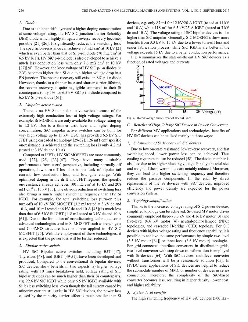
devices, e.g. only 87 mJ for 12 kV/20 A IGBT (tested at 11 kV and 10 A) while 118 mJ for 6.5 kV/25 A IGBT (tested at 3 kV dc and 10 A). The voltage rating of SiC bipolar devices is also higher than SiC unipolar. Generally, SiC MOSFETs show more benefits from 3.3 kV to 15 kV due to a lower turn-off loss and easier fabrication process while SiC IGBTs are better if the voltage exceeds 15 kV due to a better conduction performance.
Fig. 4 summarizes the state-of-the-art HV SiC devices as a function of rated voltages and currents.
Voltage (kV)5 10 15 20
Cur
rent
(A)
10
20
30
40
50
DiodeMOSFET
IGBT
JFETBJT
Thyristor
Fig. 4. Rated voltage and current of HV SiC dies.
C. Benefits of High Voltage SiC Device in Power Converters For different MV applications and technologies, benefits of
HV SiC devices can be utilized mainly in three ways:
1) Substitution of Si devices with SiC devices Due to low on-state resistance, low reverse recovery, and fast
switching speed, lower power loss can be achieved. Thus cooling requirement can be reduced [58]. The device number is also less due to its higher blocking voltage. Finally, the total size and weight of the power module are notably reduced. Moreover, they can lead to a higher switching frequency and therefore reduce the passive components. In the end, by direct replacement of the Si devices with SiC devices, improved efficiency and power density are expected for the power conversion system.
2) Topology simplification Thanks to the increased voltage rating of SiC power devices,
simplified topology can be achieved. Si-based MV motor drives commonly employed three- (3.3 kV and 4.16 kV motor [3]) and five-level (6.6 kV motor [4]) neutral-point-clamped (NPC) topologies, and cascaded H-bridge (CHB) topology. For SiC devices with higher voltage rating and frequency capability, it is possible to achieve the same performance by simple two-level (3.3 kV motor [64]) or three-level (6.6 kV motor) topologies. For grid-connected interface converters in distribution grids, two-level converter with step-down transformation is employed with Si devices [64]. With SiC devices, multilevel converter without transformer will be a reasonable solution [65]. In HVDC area, applications of SiC devices are helpful to reduce the submodule number of MMC or number of devices in series connection. Therefore, the complexity of the SiC-based converter becomes less, resulting in higher density, lower cost, and higher reliability.
3) System level benefits The high switching frequency of HV SiC devices (500 Hz –
JI et al. : OVERVIEW OF HIGH VOLTAGE SIC POWER SEMICONDUCTOR DEVICES: DEVELOPMENT AND APPLICATION 257
1 kHz of HV Si devices compared to 5 kHz – 10 kHz of HV SiC devices) brings system level benefits.
In MV motor drives, system configuration modification is allowed with high switching frequency HV SiC devices. For example, for applications requiring or favoring high rotation speeds (e.g. compressors), HV SiC can enable high speed direct motor drives, leading to elimination of gearbox and associated accessories, and then increased power density, smaller footprint, reduced maintenance, high reliability, and potentially lower system cost. The estimated footprint reduction is up to 60% in footprint size compared with the low-speed drive system with gearbox [66].
High switching frequency and control bandwidth bring significant benefits in grid-connected converters. Some grid functions can be improved due to high frequency SiC devices. For example, the operation transient, including low voltage ride through, transition between different modes, fault clearance, and black start, shows better transient performance with a higher control bandwidth. Higher switching frequency and control bandwidth also enable new grid functions such as operating as active power filter to improve power quality [67] and stabilizer to enhance system stability [68].
III. CHALLENGES OF HV SIC DEVICE Even though the HV SiC devices show better performance
compared to their Si counterparts, special considerations need to be taken into account in order to utilize them efficiently and reliably. The HV SiC device application has to overcome the challenges in different time scale. Most of challenges come from very small time scale from 0.01-1 μs, such as the gate drive design, packaging and EMI. If the problem of the HV SiC devices in the small time scale is perfectly solved, the SiC-based converter can feature benefits in output with high frequency range, low total harmonic distortion (THD), high control bandwidth, etc. The application technology of HV SiC devices is not mature and is still an active research area. Several key topics are discussed below.
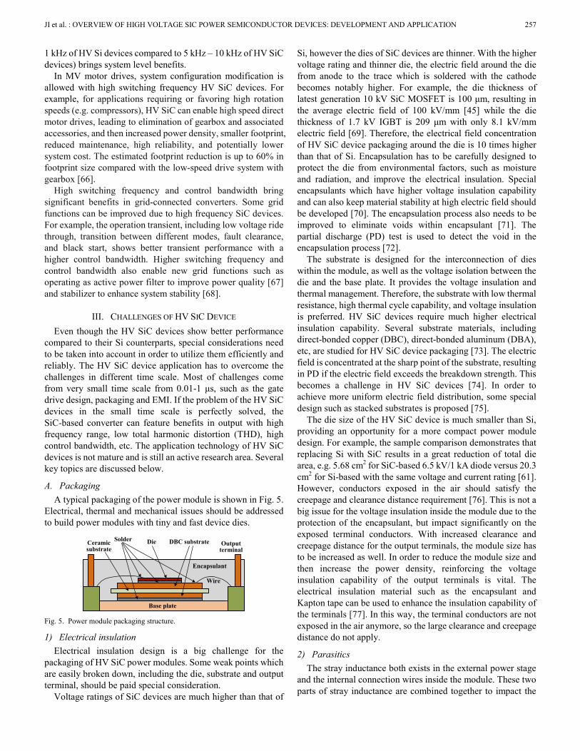
A. Packaging A typical packaging of the power module is shown in Fig. 5.
Electrical, thermal and mechanical issues should be addressed to build power modules with tiny and fast device dies.
Die
Base plate
Solder DBC substrateCeramic substrate
Wire
Output terminal
Encapsulant
Fig. 5. Power module packaging structure.
1) Electrical insulation Electrical insulation design is a big challenge for the
packaging of HV SiC power modules. Some weak points which are easily broken down, including the die, substrate and output terminal, should be paid special consideration.
Voltage ratings of SiC devices are much higher than that of
Si, however the dies of SiC devices are thinner. With the higher voltage rating and thinner die, the electric field around the die from anode to the trace which is soldered with the cathode becomes notably higher. For example, the die thickness of latest generation 10 kV SiC MOSFET is 100 μm, resulting in the average electric field of 100 kV/mm [45] while the die thickness of 1.7 kV IGBT is 209 μm with only 8.1 kV/mm electric field [69]. Therefore, the electrical field concentration of HV SiC device packaging around the die is 10 times higher than that of Si. Encapsulation has to be carefully designed to protect the die from environmental factors, such as moisture and radiation, and improve the electrical insulation. Special encapsulants which have higher voltage insulation capability and can also keep material stability at high electric field should be developed [70]. The encapsulation process also needs to be improved to eliminate voids within encapsulant [71]. The partial discharge (PD) test is used to detect the void in the encapsulation process [72].
The substrate is designed for the interconnection of dies within the module, as well as the voltage isolation between the die and the base plate. It provides the voltage insulation and thermal management. Therefore, the substrate with low thermal resistance, high thermal cycle capability, and voltage insulation is preferred. HV SiC devices require much higher electrical insulation capability. Several substrate materials, including direct-bonded copper (DBC), direct-bonded aluminum (DBA), etc, are studied for HV SiC device packaging [73]. The electric field is concentrated at the sharp point of the substrate, resulting in PD if the electric field exceeds the breakdown strength. This becomes a challenge in HV SiC devices [74]. In order to achieve more uniform electric field distribution, some special design such as stacked substrates is proposed [75].
The die size of the HV SiC device is much smaller than Si, providing an opportunity for a more compact power module design. For example, the sample comparison demonstrates that replacing Si with SiC results in a great reduction of total die area, e.g. 5.68 cm2 for SiC-based 6.5 kV/1 kA diode versus 20.3 cm2 for Si-based with the same voltage and current rating [61]. However, conductors exposed in the air should satisfy the creepage and clearance distance requirement [76]. This is not a big issue for the voltage insulation inside the module due to the protection of the encapsulant, but impact significantly on the exposed terminal conductors. With increased clearance and creepage distance for the output terminals, the module size has to be increased as well. In order to reduce the module size and then increase the power density, reinforcing the voltage insulation capability of the output terminals is vital. The electrical insulation material such as the encapsulant and Kapton tape can be used to enhance the insulation capability of the terminals [77]. In this way, the terminal conductors are not exposed in the air anymore, so the large clearance and creepage distance do not apply.
2) Parasitics The stray inductance both exists in the external power stage
and the internal connection wires inside the module. These two parts of stray inductance are combined together to impact the

258 CES TRANSACTIONS ON ELECTRICAL MACHINES AND SYSTEMS, VOL. 1, NO. 3, SEPTEMBER 2017
device’s switching performance. Both of them should be minimized. The effect of the stray inductance in the external power stage can be eliminated by decoupling capacitor [45]. This subsection focuses on the stray inductance inside the module. Their impacts on device’s performance mainly come from three aspects, voltage overshoot, ringing, and switching speed limitation.
Due to a very high di/dt for HV SiC devices, the voltage overshoot during the turn-off transient caused by the stray inductance can be notably larger than Si (e.g. 10 A/ns in 10 kV/240 A SiC MOSFET corresponding to a voltage spike rate of 10 V/nH [62]). The oscillation between the stray inductor and the parasitic capacitor of the device worsens the electro-magnetic interference (EMI) and results in additional switching loss as well [78]. Lower stray inductance is attractive to reduce the voltage overshoot and oscillation.
Switching speed is adversely affected by the stray inductance coupled between gate loop and power loop, i.e. common source inductance [79]. Kelvin connection which separates the power and signal source is applied in order to reduce the inductance in the gate drive loop [80].
In conventional low-speed HV Si devices, the impact of the anode-cathode parasitic capacitance on switching performance is very small, considering the low dv/dt and its resultant displacement current flowing through the capacitance during switching transients is negligible. Their switching speed is mainly decided by the anode-gate capacitance (i.e., Miller capacitance) and gate drive parameters [60]. This changes in high-speed HV SiC devices while the anode-cathode capacitance plays a major role especially during the turn-off transient [45]. The anode-cathode capacitance is practically the sum of the die parasitic capacitance and package capacitance between the die and cooling system. The switching loss notably increases with the package capacitance. Additionally, the high dv/dt can result in common-mode (CM) current flowing through the parasitic capacitance during switching transients (37.5 A in three-phase voltage source inverter reported in [81]).
The parasitic capacitance of the package is mainly decided by the area of critical output trace which experiences high dv/dt. For example, in the discrete MOSFET module, the critical output trace is trace connected with the cathode of the upper device and the anode of the lower device. In the half-bridge and H-bridge MOSFET module, it is the trace connected with the midpoint of the bridge. Optimizing the output trace design can minimize the parasitic capacitance of the package [82]. The thickness and permittivity of the substrate also greatly affect the parasitic capacitance.
3) Power module with multi-dies Due to the limited current rating of the single die of existing
HV SiC device (commonly around 20 A per die), it is necessary to develop the multi-die in parallel connection for HV SiC-based power modules. For example, the 10 kV/240 A SiC MOSFET power module consists of 18 dies in the parallel connection [62]. The positive coefficient of on-state resistance for most SiC devices allows the paralleled dies achieving current balance sharing naturally in static state. However, the
dynamic current may not be balanced during the switching transient. Asymmetrical parasitic inductance among paralleled dies both in power loop and gate loop can result in significant current imbalance [83-85]. Consequently, the dies with higher switching loss tend to have shorter lifetime than other dies, limiting the lifetime of the power module. Symmetrical layout of power loop and gate loop of paralleled dies is critical to achieve the same parasitic inductance between these dies.
Because the HV SiC device have a much smaller die size compared to their Si counterparts, it is possible to build the half-bridge or full-bridge in a power module even though at high voltage ratings. These power modules have higher power density compared to discrete HV Si power modules. For example, the power density of the half-bridge power module with the 10 kV/240 A SiC MOSFET reaches 4.2 W/mm3 while the power density using discrete 6.5 kV/250 A Si IGBT module is 2.2 W/mm3 [25]. Fig. 6 shows the picture of SiC and Si power modules. Integrating the half bridge in a power module can also reduce the parasitic inductance. The 10 kV/240 A achieves 16 nH which is much less than the inductance of the connection through bus bar and electric cable. The challenge is the die and bonding wire layout for the minimization of the power loop area, and then the stray inductance of the package. The active switch and antiparallel diode of the complementary switch should be placed as close as possible. The antiparallel JBS diodes are commonly used for Wolfspeed/Cree 1st and 2nd generation MOSFETs due to the low reliability of their body diodes. The current is commutated between the MOSFET and the antiparallel JBS diode of its complementary MOSFET. While the JBS diode can be eliminated in Wolfspeed/Cree 3rd generation MOSFETs due to the highly improved reliability of their body diode, resulting in a commutation loop between two MOSFETs. The elimination of the anti-parallel JBS diode causes difference of the die layout with old and new generation MOSFETs.
195 mm125 mm
23.5 mm
140 mm
36.5 mm
73 mm (a) 10 kV/240 A SiC MOSFET (b) 6.5 kV/250 A Si IGBT
Fig. 6. Si and SiC power modules.
B. Gate drive The gate drive is the interface between the power
semiconductor device and control. The control signal is transferred to drive signal through the gate drive to turn-on and turn-off power semiconductors. Gate drive design is very important to fully utilize the potential benefits of SiC devices. Efficiency and reliability are two critical aspects, and should be both considered in the gate drive design. As novel power devices, the HV SiC devices do not have commercial gate drives available. Research related to its gate drive is necessary. Some key issues in gate drive design are discussed below.
1) Basic design The basic structure of the gate drive is shown in Fig. 7.

JI et al. : OVERVIEW OF HIGH VOLTAGE SIC POWER SEMICONDUCTOR DEVICES: DEVELOPMENT AND APPLICATION 259
Isolated power supply, signal isolator, gate drive IC, as well as the gate resistance selection should be carefully considered in the basic design.
Gate drive IC
Signal isolator
Isolated power supply
Gate resistance
Control signal
Input power Fig. 7. Basic structure of gate drive.
Because gate drive power supplies for different power semiconductors in the power converter share the same input while their outputs are different, the voltage isolation between the input and output is required. Generally, the isolated power supply consists of isolated transformer and flyback converters in preliminary and secondary sides [86]. Voltages in two sides are isolated by the transformer. The isolation voltage of the transformer should exceed the voltage rating of the power semiconductor. Considering the rated voltage of the SiC device is much higher than Si, the commercial isolated power supplies are not suitable for HV SiC devices [87]. The transformer design with high insulation voltage and compact size is necessary. The high voltage transformer using Kapton tape and silicon gel as insulation material are used for HV SiC devices in [65]. The coupling capacitance between preliminary and secondary sides, which causes significant CM current if high dv/dt happens at gate terminal during switching transients, is a key parameter of isolated transformer specifications. The parasitic capacitance of isolated transformer in HV SiC devices should be much lower considering a significant increasing dv/dt of HV SiC devices (50 V/ns in SiC while only 3 V/ns in Si).
Similarly, the control signal needs to isolate from gate drive signal. The optic fiber, which has very high insulation voltage and dv/dt immunity, is the best choice as the signal isolator for HV SiC devices.
As the direct interface with the gate terminal, the gate drive IC is the key component for switching performance. The gate drive ICs for different types of devices are quite different. BJT is current-driven while JFET, MOSFET and IGBT are voltage-driven, resulting in different types of gate drive ICs. Among voltage-driven devices, the JFETs present lower gate threshold, as well as lower positive voltage of the gate drive than the MOSFETs and IGBTs due to an intrinsic diode between gate terminal and source terminal [88]. The gate drive IC design is highly relied on the device output characteristics. Considering the MOSFETs and IGBTs are most common used HV SiC devices, they are selected as an example for a detailed gate drive IC design in the paper.
Push-pull topology is often applied in these gate drive ICs. Some critical parameters of the gate drive IC including positive and negative bias voltages, output resistance of the buffer and average power rating. The positive and negative bias voltage should be high enough to make sure the device can operate in the ohmic region effectively in on-state and keep off reliably in off-state. However, the maximum gate voltage is also limited
by the mean-time-between-failures (MTBF) versus gate voltage stress curve. With the increased gate bias voltage, the device will be easily degraded, causing a shorter lifetime (e.g. a decrease of MTBF from 107 hours at 20 V to 5×10⁵ hours at 25 V) [89]. Meanwhile, the continuous high voltage will cause a gate threshold shift due to the trapped holes effect [90]. Especially when high negative voltage is applied to the gate for an extended period of time, the gate threshold will drop significantly. Consequently, the negative bias of HV SiC devices is much lower than Si. For example, a gate drive voltage of +15 V/-5 V is recommended for Wolfspeed/Cree 3rd generation MOSFETs CPM3-10000-0350-ES. The buffer resistance is included as the lumped gate resistance. There is a strict limitation for the maximum buffer resistance in very fast switching devices. In HV SiC devices, the normal buffer resistance is still allowed but should be considered in the gate resistance design.
The lumped gate resistance consists of the internal gate resistance of the device (ohmic contact), the output resistance of gate drive buffers and external gate resistance designed by users. The relationship between switching performance and gate resistance of HV SiC MOSFETs has been studied [45], presenting a large difference with low-speed Si devices. For HV SiC devices, the switching speed during the turn-off transient is mainly limited by the anode-cathode capacitance, therefore a small turn-off gate resistance can be used to achieve a shorter turn-off delay. The switching speed during the turn-on transient is highly relied on the gate resistance. The turn-on resistance should be selected based on the dv/dt susceptibility of the power electronic system.
2) Protection Similar to Si devices, the protection for over- and
under-voltage of power supply, over-voltage of device, and over-current and short circuit of device, should be integrated into the gate drive of the HV SiC devices.
Among them, the over-current and short circuit protection is most critical and challenging, due to a limited short circuit withstand time of the HV SiC device. The short circuit performances of LV SiC MOSFET [91], JFET [92] and BJT [93] have been presented and compared [94]. However, for HV SiC devices, only the MOSFET has a reliable short circuit capability [44] while the short circuit performances of the JFET, BJT and IGBT have not been reported. Different from Si IGBTs, the saturation current of HV SiC MOSFETs in the active region increases with drain-source voltage due to its short-channel effects [95], resulting in a much higher short circuit current. For example, the short circuit current of 10 kV SiC MOSFET can reach 20 times of the rated current at 5 kV dc-link [43] while only 7 times for conventional HV Si IGBT [96]. Therefore, the HV SiC MOSFET suffers a higher instantaneous power during short circuit, thus probably has a shorter short circuit withstand time. The ordinary 10 kV SiC MOSFET can only survive within 2 μs when the short circuit happens, requiring a fast response for the short circuit protection. The commercial gate drives of Si IGBTs has a response time of 12 μs [97] and cannot satisfy the requirement

260 CES TRANSACTIONS ON ELECTRICAL MACHINES AND SYSTEMS, VOL. 1, NO. 3, SEPTEMBER 2017
of SiC devices. It is difficult to achieve fast response time and strong noise immunity simultaneously considering there is a trade-off between them. Some short circuit protection schemes, such as the improved desaturation technique and over-current protection based on integrated current sensor [40], have been proposed for HV SiC MOSFETs. Some efforts to increase the short circuit capability of power semiconductors are also conducted. Recently, the 10 kV SiC MOSFET with enhanced short circuit capability (>10 µs short circuit withstand time) is reported [25].
The voltage spike during the turn-off transient will cause the breakdown of the device. In a phase-leg configuration, the over-voltage also happens during the turn-on transient of its complementary device. These problems become more serious in the HV SiC devices due to fast switching speed. Avalanche ruggedness is an important feature for a power device which is determined by its ability to dissipate avalanche energy without catastrophic device failure when excessive over-voltage is applied [98]. It has been reported that the LV SiC devices have good avalanche ruggedness in terms of the avalanche energy (e.g. 3.5 mJ for 1.2 kV/98 A MOSFET with a die size of 26 mm2 [99]). However, the avalanche ruggedness of HV SiC devices is still unknown. The over-voltage protection such as active gate clamping circuit is necessary and the optimization for the stray inductance of the power stage is also needed.
3) Cross-talk Cross-talk issue refers to the interference of the lower and
upper devices in a phase-leg configuration. With increased dv/dt during the turn-on transient, gate-source voltage of its complementary device may be charged higher than the gate threshold voltage through its Miller capacitance. This positive spurious gate voltage may generate a shoot-through current, flowing from the upper device to the lower one. The conducting current and turn-on loss of the lower device will increase due to the shoot through current. Therefore, if crosstalk happens, the switching performance becomes worse with increasing dv/dt. Similarly, during the turn-off transient, a negative spurious gate voltage would be induced, leading to degradation of the switch if its magnitude exceeds the maximum allowable negative biased gate voltage of the semiconductor device. Cross-talk is negligible in HV Si devices due to their low switching speed. For the HV SiC devices, the cross-talk issue may become a limitation for the switching speed both during the turn-on and turn-off transients, and its impact should be estimated. In order to fully utilize the fast speed of the HV SiC devices, an anti-cross-talk circuit may be needed in the gate drive.
The cross-talk issue is a major limitation of the switching speed in the LV SiC devices. Therefore, the anti-cross-talk circuit is necessary in the gate drive of LV SiC devices. Several anti-cross-talk schemes including gate impedance control and gate voltage control have been proposed [100]. Additional auxiliary switches are required in gate drive and their control signals with the gate drive signal should be phased properly. The cross-talk in the HV SiC devices is not as strict as that in the LV SiC devices due to a smaller Cgd/Cgs ratio (e.g. 0.7×10⁻³ in 10 kV SiC MOSFET compared to 5.4×10⁻³ in 1.2 kV SiC
MOSFET using measured data at 1 kV drain-source voltage) [45]. The effect of the cross-talk can be roughly estimated based on the parasitic capacitance versus drain-source voltage curve. With the curve, the maximum gate voltage change can be calculated by assuming that all the current flowing though the Miller capacitance of the device charges its gate-source capacitance. The anti-cross-talk circuit is required if the calculated spurious gate voltage will threaten the switching speed.
C. EMI Because the high dv/dt induced by the fast switching speed
and the large parasitic capacitance due to the compact size, the converters using HV SiC devices may suffer severe EMI. EMI filter is necessary and special technology for EMI reduction is also attractive.
Due to the low switching frequency of the HV Si devices (lower than 1 kHz), only a few pulse width modulation (PWM) methods, such as space vector (SV) PWM, selected harmonic elimination (SHE) PWM are applied in the Si-based converters to satisfy power quality requirement. With the increasing switching frequency up to 20 kHz, more PWM methods can be considered in the SiC-based converters. Several PWM techniques proposed to reduce the EMI by decreasing the CM voltage, such as near state (NS) PWM [101], active zero state (AZS) PWM [102], are possible in MV SiC-based converters. The variable switching frequency PWM, which causes the spectrum, originally consisting of narrow band harmonics, to spread over the frequency range, resulting in the EMI reduction [103], is also a potential solution for the converters using the HV SiC devices.
EMI filter is the key component to make sure the converters satisfy the EMI requirement. In motor drives, the EMI and dv/dt filter is vital to protect the motor from the voltage doubling affect caused by high dv/dt [104]. In the grid applications, high dv/dt will cause serious conduction EMI in the grid side. EMI filters are needed to guarantee the power conversion system meet the requirement for grid-connected converters [105].
IV. APPLICATIONS
A. Solid State Transformer The solid state transformer (SST) can replace the bulky
line-frequency 50 or 60 Hz transformers and benefits at least in two aspects: 1) significant size and weight reduction of the system due to the replacement of the line-frequency transformer by the high frequency transformer. The magnetic core size is, as a first order approximation, inversely proportional to its operating frequency; 2) more flexible controllability due to the application of power electronic converters. Thanks to these advantages, the SST is attractive in many areas especially in MW applications, such as distribution grid [35] and high-speed train traction drives [106].
GE develops a 1 MVA, 13.8 kVac/ 265 Vac SiC-based SST under the support of the US Navy and DARPA. 10 kV/120 A SiC MOSFET half bridge module and 20 kHz high frequency transformer are applied. The modular technology is applied


262 CES TRANSACTIONS ON ELECTRICAL MACHINES AND SYSTEMS, VOL. 1, NO. 3, SEPTEMBER 2017
Drive, GE Global Research, FREEDM at North Carolina State University and CPES at Virginia Tech are acknowledged.
REFERENCES [1] ABB, [online]. Available: http: //new.abb.com /drives /medium - voltage
- ac – drives. [2] GE, [online]. Available: http: //www.gepowerconversion.com /product -
solutions/induction-motors/mv-hv-cage-induction-motors [3] Siemens, [online]. Available: http://www.industry.usa.siemens.com/
drives/us/en/electric-drives/medium-voltage-drives/pages/medium-voltage-drives.aspx.
[4] Alstom, [online]. Available: http://www.mvdrives.com/alstom-mv-drives -specifications.
[5] J. W. Schwartzenberg, R. W. Dedoncker, “15 kV medium voltage static transfer switch,” in IAS annual meeting, 1995, pp. 2515-2520.
[6] J. Haefner and B. Jacobson, “Proactive hybrid HVDC breakers - a key innovation for reliable HVDC grids,” CIGRE symposium, Sep. 2011.
[7] A. Abramovitz, K. M. Smedley, “Survey of solid-state fault current limiters,” IEEE Trans. Power Electron., vol. 27, no. 6, pp. 2770-2782, Jun, 2012.
[8] M. Zadehbagheri, N.A.Azil, A. Bagherinasab and S.Ayob, “Performance evaluation of custom power devices in power distribution networks to power quality improvement: a review,” International Journal of Scientific & Engineering Research, vol. 4, no. 5, pp. 44-49, May. 2013.
[9] M. Montero, E. Cadaval, F. Gonzalez, “Comparison of control strategies for shunt active power filters in three-phase four-wire systems,” IEEE Trans. Power Electron., vol. 22, no. 1, pp. 229-236, Jan. 2007.
[10] S. B. Kjaer, J. K. Pedersen, and F. Blaabjerg, “A review of single-phase grid-connected inverters for photovoltaic modules,” IEEE Trans. Ind. Appl., vol. 41, pp. 1292-1306, Sep./Oct. 2005.
[11] F. Blaabjerg, M. Liserre, and K. Ma, “Power electronics converters for wind turbine systems,” IEEE Trans. Ind. Appl., vol. 48, no. 2, pp. 708-719, Mar./Apr. 2012.
[12] Siemens, Available: http://www.automation.siemens.com/tip-static/dlc /en/Green-Applications/SIESTORAGE_Modular_Energy_Storage_System.pdf
[13] J. Carrasco, L. Franquelo, J. Bialasiewicz, “Power-electronic systems for the grid integration of renewable energy sources: a survey,” IEEE Trans. Ind. Electron., vol. 53, no. 4, pp. 1002-1016, Apr. 2006.
[14] R. H. Lasseter, “Microgrids,” IEEE Power Engineering Society Winter Meeting, pp. 146-149, 2001.
[15] S. Xu, A. Q. Huang, and R. Burgos, “Review of solid-state transformer technologies and their application in power distribution systems,” Emerging and Selected Topics in Power Electronics, IEEE Journal of, vol. 1, pp. 186-198, Sep. 2013.
[16] D. Das, R. Kandular, J. Munoz, “An integrated controllable network transfomer-hybrid active filter system,” IEEE Trans. Ind. Appl., vol. 51, no. 2, pp. 1692-1701, Mar./Apr. 2015.
[17] S. Zheng, J. Wang, F. Yang, F. Wang, L. Tolbert, D. Costinett, “A DC controller for continuous variable series reactors (CVSRs),” in Proc. ECCE, pp. 5786-5793, 2015.
[18] N. Flourentzou, V. Agelidis, D. Demetriades, “VSC-based HVDC power transmission systems: an overview,” IEEE Trans. Power Electron., vol. 24, no. 3, pp. 592-602, Mar. 2009.
[19] A. Hefner, S. Ryu, B. Hull, D. Berning, C. Hood, J. M. Ortiz-Rodriguez, A. Rivera-Lopez, T. Duong, A. Akuffo, M. Hernandez-Mora, “Recent advances in high-voltage, high-frequency silicon-carbide power devices,” in Proc. IAS, pp. 330-337, 2006.
[20] J. W. Palmour, “Future high voltage silicon carbide power devices,” Workshop on Future Large CO2 Compression Systems, Mar. 2009.
[21] D. Grider, A. Agarwal, S.-H. Ryu, L. Cheng, C. Capell, C. Jonas, “Advanced SiC power technology for high megawatt power conditioning,” High Megawatt Power Conditioning System Workshop, May. 2012.
[22] D. Grider, M. Das, A. Agarwal, J. Palmour, S. Leslie, J. Ostop, R. Raju, M. Schutten, A. Hefner, “10 kV/120 A SiC DMOSFET half H-bridge power modules for 1 MVA solid state power substation,” in Proc. ESTS, pp. 131-134, 2011.
[23] R. Singh, “Ultra-high voltage SiC power devices,” GeneSiC Semiconductor.
[24] USCi, [online] Available: http://unitedsic.com/custom-products/ [25] J. B. Casady, T. McNutt, D. Girder, and J. Palmour, “Medium voltage SiC
R&D update,” Wolfspeed, April 2016. [26] Y. Jiang, W. Sung, X. Song, H. Ke, S. Liu, B. Baliga, A. Huang, E. Brunt,
“10 kV SiC MPS diodes for high temperature applications,” in Proc. ISPSD, pp. 43-46, 2016.
[27] H. Niwa, G. Feng, J. Suda, T. Kimoto, “Breakdown characteristics of 15-kV-class 4H-SiC PiN diodes with various junction termination structures,” IEEE Trans. Electron Devices, vol. 59, no. 10, pp. 2748-2752, Oct. 2012.
[28] M. Das, J. Sumakeris, B. Hull, J. Richmond, S. Krishnaswami, A. Powell, “High power, drift free 4H-SiC PiN diodes,” in Proc. LECHPD, pp. 236-240, 2004.
[29] J. Hostetler, X. Li, P. Alexandrov, A. Bhalla, M. Becher, and J. Sherbondy, “6.5 kV silicon carbide JFETs switch module for high density power conversion system,” in EESAT Technical Conference, Sep. 2015.
[30] J. Bendel, and X. Li, “Using “normally on” JFETs in power system,” Bodo’s Power Systems, Mar. 2015.
[31] J. L. Hostetler, X. Li, P. Alexandrov, X. Huang, A. Bhalla, M. Becker, J. Colombo, D. Dieso, J. Sherbondy, “6.5 kV enhancement mode SiC JFET based power module,” in Proc. WiPDA, pp. 300-305, 2015.
[32] J. Hostetler, P. Alexandrov, X. Li, L. Fursin, A. Bhalla, M. Becher, F. Hoffman, J. Sherbondy, and D. Morozowich, “6.5 kV silicon carbide enhanced mode JFETs for high voltage DC link applications,” 2014.
[33] J. Casady, V. Pala, D. Lichtenwalner, E. Brunt, B. Hull, G. Wang, J. Richmond, S. Allen, D. Grider, J. Palmour, “New generation 10kV SiC power MOSFET and diodes for industrial applications,” in Proc. PCIM, pp. 1-8, 2015.
[34] Q. Zhang, R. Callanan, M. Das, S. Ryu, A. Agarwal. J. Palmour, “SiC Power devices for microgrids,” IEEE Trans. Power Electron., vol. 25, no. 12, pp. 2889-2896, Dec. 2010.
[35] A. Huang, L. Wang, Q. Tian, Q. Zhu, D. Chen, W. Yu, “Medium voltage solid state transformers based on 15 kV SiC MOSFET and JBS diode,” in Proc. IECON, pp. 6996-7002, 2016.
[36] A. Q. Huang, “FREEDM system - a vision for the future grid,” in Proc. PES, pp. 1-4, 2010.
[37] J. Palmour, L. Cheng, V. Pala, E. V. Brunt, D. J. Lichtenwalner, G. Wang, J. Richmond, M. O’Loughlin, S. Ryu, S. T. Allen, A. A. Burk, C. Scozzie, “Silicon carbide power MOSFETs: breakthrough performance from 900 V up to 15 kV,” in Proc. ISPSD, pp. 79-82, 2014.
[38] S. Ryu, S. Krishnaswami, B. Hull, J. Richmond, A. Agarwal, A. Hefner, “10 kV, 5A 4H-SiC power DMOSFET,” in Proc. ISPSD, pp. 1-4, 2006.
[39] J. Wang, T. Zhao, J. Li, A. Q. Huang, R. Callanan, F. Husna, A. Agarwal, “Characterization, modeling, and application of 10-kV SiC MOSFET,” IEEE Trans. Electron Devices, vol. 55, no. 8, pp. 1798-1806, Aug. 2008.
[40] S. Ji, S. Zheng, Z. Zhang, F. Wang, L. Tolbert, “Protection and temperature-dependent switching characterization of latest generation 10 kV SiC MOSFETs,” in Proc. APEC, pp. 783-788, 2017.
[41] X. Zhang, H. Li, J. Brothers, J. Wang, L. Fu, M. Perales, J. Wu, “A 15-kV SiC MOSFET gate driver with a laser-light-over-fiber based isolated power supply and comprehensive protection functions,” in Proc. APEC, pp.1967-1973, 2016.
[42] E. Eni, B. I. Incau, T. Kerekes, R. Teodorescu, S. Nielsen, “Characterisation of 10 kV 10 A SiC MOSFET,” in Proc. ACEMP, pp. 675-680, 2015.
[43] E. Eni, S. Beczkowski, S. Nielsen, T. Kerekes, R. Teodorescu, R. Juluri, B. Julsgaard, E. VanBrunt, B. Hull, S. Sabri, D. Grider, C. Uhrenfeldt, “Short-circuit degradation of 10 kV 10 A SiC MOSFET,” IEEE Trans. Power Electron., 2017.
[44] E. Eni, S. Beczkowski, S. Nielsen, T. Kerekes, R. Teodorescu, “Short-circuit characterization of 10 kV 10A 4H-SiC MOSFET,” in Proc. APEC, pp. 974-978, 2016.
[45] S. Ji, S. Zheng, F. Wang, L. Tolbert, “Temperature-dependent characterization, modeling and switching speed limitation analysis of third generation 10 kV SiC MOSFET,” IEEE Trans. Power Electron., 2017.
[46] K. Vechalapu, S. Bhattacharya, “Performance comparison of 10 kV-15 kV high voltage SiC modules and high voltage switch using series

JI et al. : OVERVIEW OF HIGH VOLTAGE SIC POWER SEMICONDUCTOR DEVICES: DEVELOPMENT AND APPLICATION 263
connected 1.7 kV LV SiC MOSFET devices,” in Proc. ECCE, pp. 1-8, 2016.
[47] H. Miyake, T. Okuda, H. Niwa, T. Kimoto, J. Suda, “21-kV SiC BJTs with space-modulated junction termination extension,” IEEE Electron Device Letters, vol. 33, no. 11, pp. 1598-1600, Nov. 2012.
[48] X. Song, A. Huang, M. Lee, C. Peng, “Theoretical and experimental study of 22 kV SiC emitter turn-OFF (ETO) Thyristor,” IEEE Trans. Power Electron., vol. 32, no. 8, pp. 6381-6393, Aug. 2017.
[49] Q. Zhang, M. Das, J. Sumakeris, R. Callanan, A. Agarwal, “12-kV p-channel IGBTs with low on-resistance in 4H-SiC,” IEEE Electron Device Letters, vol. 29, no. 9, pp. 1027-1029, Sep. 2008.
[50] S. Ryu, C. Capell, L. Cheng, C. Jonas, A. Gupta, M. Donofrio, J. Clayton, M. O’Loughlin, A. Burk, D. Grider, A. Agarwal, J. Palmour, A. Hefner, S. Bhattacharya, “High performance, ultra high voltage 4H-SiC IGBTs,” in Proc. ECCE, pp. 3603-3608, 2012.
[51] Y. Yonezawa, T. Mizushima, K. Takenaka, H. Fujisawa, T. Kato, S. Harada, “Low V/f and highly reliable 16 kV ultrahigh voltage SiC flip-type n-channel implantation and epitaxial IGBT,” in Proc. IEDM, pp. 661-664, 2013.
[52] I. Cvetkovic, Z. Shen, M. Jaksic, C. Dimarino, F. Chen, D. Boroyevich, R. Burgos, “Modular scalable medium-voltage impedance measurement unit using 10 kV SiC MOSFET PEBBs,” in Proc. ESTS, pp. 326-331, 2015.
[53] Q. Xiao, Y. Yan, X. Wu, N. Ren, K. Sheng, “A 10 kV / 200 A SiC MOSFET module with series-parallel hybrid connection of 1200 V / 50 A dies,” in Proc. ISPSD, pp. 349-352, 2015.
[54] T. Duong, A. Lopez, A. Hefner, J. Rodriguez, “Circuit simulation model for a 100 A, 10 kV half-bridge SiC MOSFET/JBS power module,” in Proc. APEC, pp. 913-917, 2008.
[55] S. Madhusoodhanan, K. Mainali, A. Tripathi, K. Vechalapu, S. Bhattacharya, “Medium voltage (>2.3 kV) high frequency three-phase two-level converter design and demonstration using 10 kV SiC MOSFETs for high speed motor drive applications,” in IEEE Proc. APEC, pp. 1496-1504, 2016.
[56] “SiC power devices and modules,” Rohm Semiconductor Co., Appl. Note 13103EAY01, Jun. 2013.
[57] S. Xu, A. Q. Huang, and R. Burgos, “Review of solid-state transformer technologies and their application in power distribution systems,” Emerging and Selected Topics in Power Electronics, IEEE Journal of, vol. 1, pp. 186-198, Sep. 2013.
[58] S. Madhusoodhanan, K. Mainali, A. K. Tripathi, A. Kadavelugu, D. Patel, S. Bhattacharya, “Power loss analysis of medium-voltage three-phase converters using 15-kV/40-A SiC N-IGBT,” Emerging and Selected Topics in Power Electronics, IEEE Journal of, vol. 4, no. 3, pp. 902-917, Mar. 2016.
[59] L. Wang, Q. Zhu, W. Yu, A. Q. Huang, “A medium-voltage medium-frequency isolated DC–DC converter based on 15-kV SiC MOSFETs,” Emerging and Selected Topics in Power Electronics, IEEE Journal of, vol. 5, no. 1, pp. 100-109, Jan. 2017.
[60] S. Ji, Z. Zhao, T. Lu, L. Yuan, H. Yu, “HVIGBT physical model analysis during transient,” IEEE Trans. Power Electron., vol. 28, no. 5, pp. 2616-2624, May. 2013.
[61] F. Filsecker, R. Alvarez, S. Bernet, “Comparison of 6.5 kV silicon and SiC diodes,” in Proc. ECCE, pp. 2261-2267, 2012.
[62] B. Passmore, Z. Cole, B. McGee, M. Wells, J. Stabach, J. Bradshaw, T. McNutt, E. VanBrunt, B. Hull, D. Grider, “The next generation of high voltage (10 kV) silicon carbide power modules,” in Proc. WiPDA, pp. 1-4, 2016.
[63] M. K. Das, C. Capell, D. E. Grider, S. Leslie, J. Ostop, R. Raju, M. Schutten, J. Nasadoski, A. Hefner, “10 kV, 120 A SiC half H-bridge power MOSFET modules suitable for high frequency, medium voltage applications,” in Proc. ECCE, pp. 2689-2692, 2011.
[64] ABB, [online]. Available: http://new.abb.com/power-converters- inverters/solar
[65] S. Madhusoodhanan, A. Tripathi, D. Patel, K. Mainali, A. Kadavelugu, S. Hazra, S. Bhattacharya. K. Hatua, “Solid-state transformer and MV grid tie applications enabled by 15 kV SiC IGBTs and 10 kV SiC MOSFETs based multilevel converters,” in IEEE Trans. Ind. Appl., vol. 51, no. 4, pp. 3343-3360, Jul./Aug. 2015.
[66] F. Wang and L. M. Tolbert, ‘‘SiC high-speed MV direct drive vs. Si low-speed MV drive in compressor applications,’’ presented at the HMW Drive Workshop II NIST, Gaithersburg, MD, USA, 2014.
[67] R. Crosier, S. Wang, “DQ-frame modeling of an active power filter integrated with a grid-connected, multifunctional electric vehicle charging station,” IEEE Trans. Power Electron., vol. 28, no. 12, pp. 5702-5716, Dec. 2013.
[68] N. Bottrell, M. Prodanovic, and T. C. Green, “Dynamic stability of a microgrid with an active load,” IEEE Trans. Power Electron., vol. 28, no. 11, pp. 5107-5119, Nov. 2013.
[69] ABB, [online]. Available: https://library.e.abb.com/public/70d72c57 fd3946bb8f9f125e8cbc7e74/ABB_Flyer_Chips_2015_Web.pdf
[70] Y. Yao, Z. Chen, G. Lu, D. Boroyevich, K. D. T. Ngo, “Characterization of encapsulants for high-voltage high-temperature power electronic packaging,” IEEE Trans. Compon. Packag. Manuf., vol. 2, no. 4, pp. 539-547, Apr. 2012.
[71] B. Grummel, R. McClure, L. Zhou, A. P. Gordon, L. Chow, Z. Shen, “Design consideration of high temperature SiC power modules,” in Proc. IECON, pp. 2861-2866, 2008.
[72] T. Lebey, S. Dinculescu, D. Malec, “Partial discharges testing of power modules,” in Proc. ICSD, pp. 896-899, 2004.
[73] D. P. Hamilton, S. Riches, M. Meisser, L. Mills, P. Mawby, “High temperature thermal cycling performance of DBA, AMB and thick film power module substrates,” in Proc. CIPS, pp. 1-5, 2016.
[74] J. H. Fabian, S. Hartmann, A. Hamidi, “Partial discharge failure analysis of AlN substrates for IGBT modules,” in European Symposium on Reliability of Electron Devices, pp. 1425-1430, 2004.
[75] O. Hohlfeld, R. Bayerer, T. Hunger, H. hartung, “Stacked substrates for high voltage applications,” in Proc. CIPS, pp. 1-4, 2012.
[76] “Standard for Insulation Coordination Including Clearances and Creepage Distances for Electrical Equipment,” UL 840, 2007.
[77] M. Wang, F. Luo, L. Xu, “A double-end sourced wire-bonded multi chip SiC MOSFET power module with improved dynamic current sharing,” Emerging and Selected Topics in Power Electronics, IEEE Journal of, 2017.
[78] T. Liu, R. Ning, T. Wong, Z. Shen, “Modeling and analysis of SiC MOSFET switching oscillations,” Emerging and Selected Topics in Power Electronics, IEEE Journal of, vol. 4, no. 3, pp. 747-756, Mar. 2016.
[79] Z. Liang, P. Ning, F. Wang, and L. Marlino, “Planar bond all: A new packaging technology for advanced automotive power modules,” in Proc. ECCE, 2012, pp. 438–443.
[80] S. Li, L. M. Tolbert, F. Wang, and F. Z. Peng, “Stray inductance reduction of commutation loop in the P-cell and N-cell-based IGBT phase leg module,” IEEE Trans. Power Electron., vol. 29, no. 7, pp. 3616–3624, Jul. 2014.
[81] A. Shima, H. Shimizu, Y. Mori, M. Sagawa, K. Konishi, R. Fujita, T. Ishigaki, N. Tega, K. Kobayashi, S. Sato, Y. Shimamoto, “3.3 kV 4H-SiC DMOSFET with highly reliable gate insulator and body diode,” in Proc. ECSCRM, 2016.
[82] Z. Chen, D. Boroyevich, and R. Burgos, “Experimental parametric study of the parasitic inductance influence on MOSFET switching characteristics,” in Proc. IPEC, pp. 164–169, 2010.
[83] R. Wu, L. Smirnova, H. wang, F. Iannuzzo, F. Blaabjerg, “Comprehensive investigation on current imbalance among parallel chips inside MW-scale IGBT power modules,” in Proc. ECCE Asia, pp. 850-856, 2015.
[84] A. Castellazzi, “Comprehensive Compact Models for the Circuit Simulation of Multichip Power Modules,” IEEE Trans. Power Electron., vol. 25, no. 5, pp. 1251-1264, May. 2010.
[85] B. Gutsmann, P. Mourick, D. Silber, “Exact inductive parasitic extraction for analysis of IGBT parallel switching including DCB-backside eddy currents,” in Proc. PESC, pp. 1291-1295, 2000.
[86] L. Ghossein, F. Morel, H. Morel, P. Dworakowski, “State of the art of gate-drive power supplies for medium and high voltage applications,” in Proc. PCIM, pp. 1-8, 2016.
[87] Concept, [online]. Available: https://www.power.com/sites/default/files/ product_document/data_sheet/ISO5125I_1.pdf
[88] C. Cai, W. Zhao, K. Sheng, “Characteristics and application of normally-off SiC-JFETs in converters without antiparallel diodes,” IEEE Trans. Power Electron., vol. 28, no. 10, pp. 4850-4860, Oct. 2013.
[89] CREE, “SiC MOSFET gate voltage selection,” Mar. 2013.

264 CES TRANSACTIONS ON ELECTRICAL MACHINES AND SYSTEMS, VOL. 1, NO. 3, SEPTEMBER 2017
[90] V. Mulpuri, S. Choi, “Reliability of SiC power MOSFETs under high repetitive pulse current conditions,” in Proc. APEC, pp. 776-782, 2017.
[91] Z. Wang, X. Shi, L. Tolbert, F. Wang, Z. Liang, D. Costinett, B. Blalock, “Temperature dependent short circuit capability of silicon carbide (SiC) power MOSFETs,” IEEE Trans. Power Electron., vol. 31, no. 2, pp. 1555-1566, Feb. 2016.
[92] X. Huang, G. Wang, Y. Li, A. Huang, B. Baliga, “Short-circuit capability of 1200 V SiC MOSFET and JFET for fault protection,” in Proc. APEC, pp. 197-200, 2013.
[93] Y. Gao, A. Huang, A. Agarwal, Q. Zhang, “Theoretical and experimental analyses of safe operating area (SOA) of 1200-v 4h-SiC BJT,” IEEE Trans. Electron Devices, vol. 55, no. 8, pp. 1887-1893, Aug. 2008.
[94] D. Sadik, J. Colmenares, G. Tolstoy, D. Peftitsis, M. Bakowski, J. Rabkowski, H. Nee, “Short-circuit protection circuits for silicon-carbide power transistors,” IEEE Trans. Ind. Electron., vol. 63, no. 4, pp. 1995-2004, Apr. 2016.
[95] B. Callanan, “Application Considerations for SiC MOSFETs,” Cree Inc., Durham, NC, USA, Jan. 2011, Cree Application Note.
[96] Mitsubishi, “CM1000HG-130XA datasheet”. [97] Concept, “1SD210F2 datasheet”. [98] A. Fayyaz, G. Romano, J. Urresti, M. Riccio, A. Castellazzi, A. Irace, N.
Wright, “A comprehensive study on the avalanche breakdown robustness of silicon carbide power MOSFETs,” Energies, vol. 10, no. 4, 2017.
[99] CREE, “CPM2-1200-0025B datasheet”. [100] Z. Zhang, F. Wang, L. Tolbert, B. Blalock, “Active gate driver for
crosstalk suppression of SiC devices in a phase-leg configuration,” IEEE Trans. Power Electron., vol. 29, no. 4, pp. 1986-1997, Apr. 2014.
[101] E. Un, A. Hava, “A near-state PWM method with reduced switching losses and reduced common-mode voltage for three-phase voltage source inverters,” IEEE Trans. Ind. Appl., vol. 45, no. 2, pp. 782-793, Mar./Apr. 2009.
[102] Y. Lai, P. Chen, H. Lee, J. Chou, “Optimal common-mode voltage reduction PWM technique for inverter control with consideration of the dead-time effects—Part I: Basic development,” IEEE Trans. Ind. Appl., vol. 40, no. 6, pp. 1613-1620, Nov./Dec. 2004.
[103] M. Kuisma, “Variable frequency switching in power supply EMI-control: an overview,” IEEE Aerospace and Electronic Systems Magazine, vol. 18, no. 2, pp. 18-22, Dec. 2003.
[104] D. Jackson, “The effect of high-speed switching on the motor insulation system,” Power Engineering Journal, pp. 174-181, Aug. 2000.
[105] “CISPR 14-1 electromagnetic compatibility – requirement for household appliances, electric tools and similar apparatus – part 1: emission,” IEC Std., 2009.
[106] J. W. Kolar, G. I. Ortiz, “Solid state transformer concepts in traction and smart grid applications,” ETH report.
[107] T. Lagier, P. Ladoux, “A comparison of insulated DC-DC converters for HVDC off-shore wind farms,” in Proc. ICCEP, pp. 33-39, 2015.
Shiqi Ji (S’10-M’15) received the B.S. and Ph.D degrees from Tsinghua University, Beijing, China, in 2010 and 2015, respectively, all in electrical engineering.
Currently, he is working as a Research Associate in CURENT, University of Tennessee, Knoxville, TN, USA. His
research interests are semiconductor device modeling, high-voltage and high-power converter design and high voltage SiC device characterization and application.
Zheyu Zhang (S’12-M’15) received B.S. and M.S. degrees from Huazhong University of Science and Technology, Wuhan, China, and the Ph.D. degree from The University of Tennessee, Knoxville, TN, USA, in 2008, 2011, and 2015, respectively, all in electrical engineering.
He is currently a Research Assistant Professor in the Department of Electrical Engineering and Computer Science at the University of Tennessee. His research interests include wide band-gap semiconductors and application, gate driver technology, motor drive design, operation, integration and reliability, and cryogenic power electronics. Dr. Zhang received two Prize Paper awards from the IEEE Industry Applications Society and IEEE Power Electronics Society.
Fei (Fred) Wang (S’85–M’91–SM’99–F’10) received the B.S. degree from Xi’an Jiaotong University, Xi’an, China, in 1982, and the M.S. and Ph.D. degrees from the University of Southern California, Los Angeles, in 1985 and 1990, respectively, all in electrical engineering.
He was a Research Scientist in the Electric Power Lab, University of Southern California, from 1990 to 1992. He joined the GE Power Systems Engineering Department, Schenectady, NY, as an Application Engineer in 1992. From 1994 to 2000, he was a Senior Product Development Engineer with GE Industrial Systems, Salem, VA. From 2000 to 2001, he was the Manager of Electronic and Photonic Systems Technology Lab, GE Global Research Center, Schenectady, NY, and Shanghai, China. In 2001, he joined the Center for Power Electronics Systems (CPES), Virginia Tech, Blacksburg, as a Research Associate Professor and became an Associate Professor in 2004. From 2003, he also served as the CPES Technical Director. Since 2009, he has been with The University of Tennessee and Oak Ridge National Lab, Knoxville, TN, as a Professor and Condra Chair of Excellence in Power Electronics. He is a founding member of the new multi-university NSF/DOE Engineering Research Center on Ultra-wide-area Resilient Electric Energy Transmission Networks (CURENT) led by The University of Tennessee. His research interests include power electronics, power systems, controls, electric machines, and motor drives.


![Semiconductor Devices [Kanaan Kano]](https://static.fdocuments.in/doc/165x107/55cf931a550346f57b9bb747/semiconductor-devices-kanaan-kano.jpg)