
Outline - BIST - University of Tokyotimcheng/NOTES/08_bist_2pp.pdf• Scan-based BIST architecture...
29
1 © K.T. Tim Cheng 08_bist, v1.0 2 © K.T. Tim Cheng 08_bist, v1.0 • Why BIST? • Memory BIST • Logic BIST pattern generator & response analyzer • Scan-based BIST architecture Outline - BIST
-
Upload
truongdang -
Category
Documents
-
view
228 -
download
2
Transcript of Outline - BIST - University of Tokyotimcheng/NOTES/08_bist_2pp.pdf• Scan-based BIST architecture...
1© K.T. Tim Cheng 08_bist, v1.0
2© K.T. Tim Cheng 08_bist, v1.0
• Why BIST?
• Memory BIST
• Logic BIST pattern generator & response analyzer
• Scan-based BIST architecture
Outline - BIST

3© K.T. Tim Cheng 08_bist, v1.0
TYPES• On-Line Self-Test (Concurrent Checking)• Functional Self-Test (system (micro)code-based)• Structural Self-Test (pseudo-random/-exhaustive, deterministic)
– Regular Structure BIST, Logic BIST, ...
OBJECTIVES OF STRUCTURAL SELF-TEST• Reduction in IC/Module Manufacturing Cost (memory/thruput)• Need for Autonomous Test at Board/Module/System Levels• Diagnostics• Burn-In
Why Built-In Self Test?
4© K.T. Tim Cheng 08_bist, v1.0
Built-In Self Test
Stimulus Source
Stored Program(1s & 0s, algorithm)
Pseudo-Random(LFSR)
CircuitUnderTest
Response Capture
& CompareStored Program
Data Compaction(CRC Signatures)
Pass/Fail
Self-TestController
Defect-FreeResponse
Compare
ClocksMode Control... including “fencing”InitializationResponse Sampling

5© K.T. Tim Cheng 08_bist, v1.0
Memory BIST
Addr
DataIn
Wen
Clk
DataOutRAM
COLLAR(Shared) RAMBISTCONTROLLER
1149.1TAP
ParametersController: global/localAlgorithmParallel Testing (multiples)DiagnosticsLoad/Unload protocol
...
6© K.T. Tim Cheng 08_bist, v1.0
OR
Memory BIST Collar
Addr
DataIn
Wen
Clk
DataOut
# Ports = # Independent AddressesEach Port is Read Only, Write Only or Read-WriteMultiPort Write Contention Resolved by Circuit Design or Address Sequencing
Compare
LOCAL RAMBISTSEQUENCER
StepperLogic
PatternLogic
OR
P/F

7© K.T. Tim Cheng 08_bist, v1.0
Ex: RAMBIST Algorithm (6N)
6N RAM test algorithm.
For address 0 to max do: W(0)For address 0 to max do: R(0), W(1), increment the addressFor address max to 0 do: R(1), W(0), R(0), decrement the address
Each location receives six operations: hence the name of the algorithm, 6N
For a byte-oriented RAM, the algorithm is repeated four times with different write
First sequence: W(0) = W(00000000), W(1) = W(11111111)Second sequence: W(0) = W(00001111), W(1) = W(11110000)Third sequence: W(0) = W(00110011), W(1) = W(11001100)Fourth sequence: W(0) = W(01010101), W(1) = W(10101010)
8© K.T. Tim Cheng 08_bist, v1.0
Test Time Complexity (100MHz)
Size N 10N NlogN N1.5 N2
1M 0.01s 0.1s 0.2s 11s 3h
16M 0.16s 1.6s 3.9s 11m 33d
64M 0.66s 6.6s 17s 1.5h 1.43y
256M 2.62s 26s 1.23m 12h 23y
1G 10.5s 1.8m 5.3m 4d 366y
4G 42s 7m 22.4m 32d 57c
16G 2.8m 28m 1.6h 255d 915c

9© K.T. Tim Cheng 08_bist, v1.0
RAM Test Algorithm
A test algorithm (or simply test) is a finite sequence of test elements.– A test element contains a number of memory
operations (access commands).» Data pattern (background) specified for the Read operation.» Address (sequence) specified for the Read and Write
operations.
A march test algorithm is a finite sequence of march elements.– A march element is specified by an address order
and a number of Read/Write operations.
10© K.T. Tim Cheng 08_bist, v1.0
March TestsMarch X– For AF, SAF, TF, & CFin.
March C [Marinescu 1982]– For AF, SAF, TF, & all CFs---redundant.
March C- [Goor 1991]– Also for AF, SAF, TF, & all CFs---irredundant.
)}0();0,1();1,0();0({ rwrwrw cc ⇓⇑
)}0();0,1();1,0();0();0,1();1,0();0({
rwrwrrwrwrw
cc
c
⇓⇓
⇑⇑
)}0();0,1();1,0();0,1();1,0();0({
rwrwrwrwrw
c
c
⇓⇓
⇑⇑

11© K.T. Tim Cheng 08_bist, v1.0
Coverage of March TestsMATS++ March X March Y March C-
SAF 1 1 1 1TF 1 1 1 1AF 1 1 1 1SOF 1 .002 1 .002CFin .75 1 1 1CFid .375 .5 .5 1CFst .5 .625 .625 1
* Extended March C- (11N) has a 100% coverage of SOF.
12© K.T. Tim Cheng 08_bist, v1.0
Testing Word-Oriented RAM
Background bit is replaced by background word.– MATS++:
Conventional method is to use log(m)+1 different backgrounds for m-bit words.– m=8: 00000000, 01010101, 00110011, and 00001111.– Apply the test algorithm logm+1=4 times, so
complexity is 4*6N/8=3N.
)},,'();',();({ rawarawarawa ⇓⇑c

13© K.T. Tim Cheng 08_bist, v1.0
Logic BIST - Stimulus GenerationThere many way to generate the test. The simplest categorization is in terms of the type of testing used:1. Exhaustive testing2. Pseudo-random testing3. Pre-stored testing
Logic BIST - Response Analysis1. Parity checking2. Transition counting3. Syndrome generation or ones counting4. Signature analysis
14© K.T. Tim Cheng 08_bist, v1.0
(a) Exhaustive test: use a counter and apply all possible patterns (2n patterns) to the circuit under test.
(b) Random test: Use linear-feedback shift register (LFSR) to apply random patterns to CUT.
Ex: TPG of random testing
D1 D2 D3+
C U T
initialvalue(seed)
D1 D2 D31 0 01 1 01 1 10 1 11 0 10 1 00 0 11 0 0This 3-stage LFSR can generate
test sequence of length 23-1=7
Test Pattern Generator for BIST

15© K.T. Tim Cheng 08_bist, v1.0
An m-stage LFSR can generate test seq. of length 2m-1— Such sequence are called maximal length sequence.— Such an LFSR is called a maximum-length LFSR.
When only a fraction of the 2m-1 can be applied, (because m is too large), LFSR is better than counters.
Cycle Counter LFSR1 0 0 0 1 0 02 0 0 1 1 1 03 0 1 0 1 1 1 4 0 1 1 0 1 15 1 0 0 1 0 16 1 0 1 0 1 07 1 1 0 0 0 18 1 1 1
Sequences of LFSR is more random: every bit is random
Maximum-Length LFSR
16© K.T. Tim Cheng 08_bist, v1.0
An LFSR Can Be Expressed by its Characteristic Polynomial f(x)
The characteristic polynomial of a maximum-length LFSR is called primitive polynomial.Several listings of such polynomials exist in the literature.
Given a CUT with m inputs, pick a primitive polynomial of degree mand construct the corresponding LFSR as a TPG.Ref: “Built-In Test for VLSI”, Paul H. Bardell et al., John Wiley & Sons, 1987 (up to degree 300).Ref: “Essential of Electronic Testing”, M. L. Bushnell, V. Agrawal, Kluwer, 2000. (pp. 620 - up to degree 100).
+
an=an-3+an-5f(x)=x5+x3+1

17© K.T. Tim Cheng 08_bist, v1.0
Characteristics of M-L LFSRThe state diagram contains two components: one contains the all-zero state, the other contains other 2m-1 states.
0000
0001 2m-1 states
For every bit, # of 1’s differs from # of 0’s by one. # of transitions between 1 and 0 in one period is (m+1)/2.
Cycle LFSR1 1 0 02 1 1 03 1 1 1 4 0 1 15 1 0 16 0 1 07 0 0 18 1 0 0
18© K.T. Tim Cheng 08_bist, v1.0
Autocorrelation between different bits:– Autocorrelation function is defined as:
The autocorrelation function of every M-L LFSR of period p=2m-1 is:– C(i,i)=1– C(i,j)=-1/p i ≠ j
C(i, j) = 1
2m − 1bi (n)b j (n)
n =1
2m −1∑
where bi (t) = 1 where ai (t) = 0bi (t ) = −1 where ai (t) = 1
⎧ ⎨ ⎩
Characteristics of M-L LFSR – Cont’d
Cycle LFSR m=31 1 0 02 1 1 03 1 1 1 4 0 1 15 1 0 16 0 1 07 0 0 1
C(1,2)=-1/7
C(1,3)=-1/7C(2,3)=-1/7
Ex. m=3:

19© K.T. Tim Cheng 08_bist, v1.0
Linear Dependency
Ref: Rajski & Tyszer, “BIST for SoC”, 1999 FTCS Tutorial
20© K.T. Tim Cheng 08_bist, v1.0
Selection of LFSR as RPTG
Degree– Large enough so the state will not repeat– Large enough to reduce linear dependencies
Type– Primitive – Avoid trinomials (increased linear dependencies)
Seed value– Select through fault simulation

21© K.T. Tim Cheng 08_bist, v1.0
Definitions - Random Pattern Testability for Logic BIST
Detection probability qi of fault fi: the probability a randomly selected input vector will detect the fault.Error latency ELi of fault fi: the number of random input vectors applied to a circuit until fi is detectedTheorem: EL of a fault has a geometric distribution.I.e Pr{ ELi = j} = (1 - qi)j-1 qi
Cumulative detection probability:FELi(t) = Pr{ELi ≤ t} = ∑t
j=1 (1 - qi)j-1 qiFELi(t) = 1 - (1 - qi)t t ≥ 1– Mean : Mi = E(ELi) = ∑∞
j=1 j (1 - qi)j-1 qi = 1/qi– Var (ELi) = E (ELi
2) - E2 (ELi) = (1 - qi)/qi2
22© K.T. Tim Cheng 08_bist, v1.0
Escape probability of a fault fi: the probability that the fault will go undetected after the application of trandom input vectors. – Similarly, escape probability of a fault set {f1, f2,…,fm} is the
probability that at least one member of the fault set will be left undetected after application of t random input vectors.
The random test length required to detect a fault fiwith escape probability no larger than a given threshold ei can be obtained as
Ti = [ln ei/ln(1 - qi)]
(Note: Pr{escape} = 1 - FELi(t) = (1 - qi)t )
Required Random Test Length as a Function of Detection & Escape Prob.
23© K.T. Tim Cheng 08_bist, v1.0
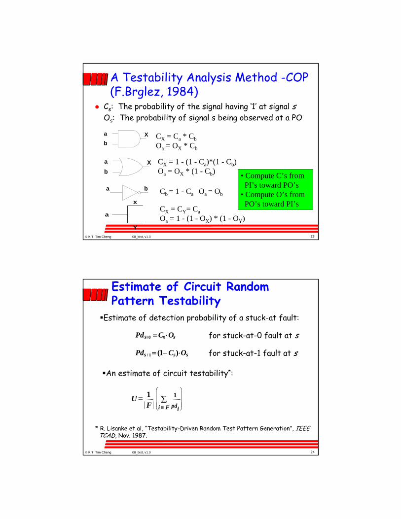
A Testability Analysis Method -COP(F.Brglez, 1984)
Cs: The probability of the signal having ‘1’ at signal sOs: The probability of signal s being observed at a PO
ab
X CX = Ca * CbOa = OX * Cb
ab
X CX = 1 - (1 - Ca)*(1 - Cb)Oa = OX * (1 - Cb)
a b Cb = 1 - Ca Oa = Ob
a
x
Y
CX = CY= CaOa = 1 - (1 - OX) * (1 - OY)
• Compute C’s from PI’s toward PO’s
• Compute O’s from PO’s toward PI’s
24© K.T. Tim Cheng 08_bist, v1.0
Estimate of Circuit Random Pattern Testability
Estimate of detection probability of a stuck-at fault:
Pd 0/s = Cs ⋅Os
Pds / 1 = (1− Cs)⋅Os
for stuck-at-0 fault at s
for stuck-at-1 fault at s
An estimate of circuit testability*:
* R. Lisanke et al, “Testability-Driven Random Test Pattern Generation”, IEEETCAD, Nov. 1987.
U = 1F
1
pdii ∈F∑
⎛
⎝
⎜⎜⎜⎜
⎞
⎠
⎟⎟⎟⎟
25© K.T. Tim Cheng 08_bist, v1.0
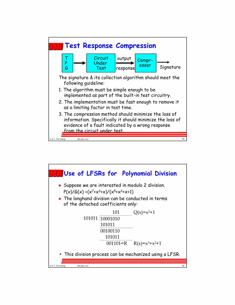
Test Response Compression
The signature & its collection algorithm should meet the following guideline:
1. The algorithm must be simple enough to be implemented as part of the built-in test circuitry.
2. The implementation must be fast enough to remove it as a limiting factor in test time.
3. The compression method should minimize the loss of information. Specifically it should minimize the loss of evidence of a fault indicated by a wrong response from the circuit under test.
CircuitUnder Test
TPG
Compr-essor Signature
output
response
26© K.T. Tim Cheng 08_bist, v1.0
Use of LFSRs for Polynomial Division
Suppose we are interested in modulo 2 division.P(x)/G(x) =(x7+x3+x)/(x5+x3+x+1)The longhand division can be conducted in terms of the detached coefficients only:
101 Q(x)=x2+1101011 10001010
10101100100110 101011 001101=R R(x)=x3+x2+1
• This division process can be mechanized using a LFSR.

27© K.T. Tim Cheng 08_bist, v1.0
When a shift occurs, x5 is replaced by x3+x1+x0.Whenever a quotient coefficient (the x5 term) is shifted off the right-most stage, x3+x1+x0 is added to the register (or subtracted from the register since addition is the same as subtraction modulo 2). Effectively, the dividend has been divided by x5+x3+ x+1.
LFSR implementing division by f(X)=x5+x3+x+1 :
+ + +
x0 x1 x2 x3 x4
input
LFSR Implementing Polynomial Division
28© K.T. Tim Cheng 08_bist, v1.0
The LFSR is initialized to zero The message word (or dividend) P(x) is serially streamed to the LFSR input, high-order coefficient first, The content of the LFSR after the last message bit is the remainder R(x) from the division of the message polynomial by the divisor G(x)– P(x) = Q(x)G(x) + R(x)
The shifted-out bit stream forms the quotient Q(x)
Using LFSR for Polynomial Division

29© K.T. Tim Cheng 08_bist, v1.0
Example: P(x)=x7+x3+x input=10001010
+ + +x0 x1 x2 x3 x4input x5
Remainder R=x3+x2+1 Quotient Q=x2+1
input
time012345678
10001010
010001111
001000010
000100001
000010101
000001010
00000101
An Example
30© K.T. Tim Cheng 08_bist, v1.0
Any data, such as the test response resulting from a circuit, can be compressed into a “signature” by an LFSR– The signature is the remainder from the division process
The LFSR is called a “signature analyzer”.– P(x)=Q(x) G(x) + R(x)
divisor signature
LFSR polynomial
LFSR As a Signature Analyzer

31© K.T. Tim Cheng 08_bist, v1.0
If P(x) is the polynomial of the correct data, any P’(x)=P(x)+M(x)G(x) will have the same signature as P(x) for any M(x).Example: P(x)=x7+x3+x G(x)=x5+x3+x+1signature R(x)=x3+x2+1P’(x)=P(x)+G(x)=x7+x5+1P’’(x)=P(x)+x•G(x)=x7+x6+x4+x3+x2
P’(x) and P’’(x) have same signature x3+x2+1.Aliasing: condition in which a faulty ckt with erroneous response produces same signature as the good circuit.Aliasing probability is usually used to measure the quality of a data compressor.
Aliasing in Signature Analysis
32© K.T. Tim Cheng 08_bist, v1.0
For an input string of m-bit long, P(x)’s degree is (m-1)There are 2m different polynomials with an degree equal to or less than (m-1).Among them, 2m-1 polynomials represent possible wrong bit streams.
For a divisor polynomial G(x) of degree r, there are 2m-r
different Q(x)’s that result in a polynomial of degree equal to or less than (m-1).• There are 2m-r-1 wrong m-bit streams that map into
the same signature as the correct bit stream.• Aliasing prob. P(M)=(2m-r -1)/(2m-1)• For large m, P(M) ≅ 1/2r.
Aliasing Prob. of Using LFSR as a Data Compressor - P(x)=Q(x) G(x)+R(x)
33© K.T. Tim Cheng 08_bist, v1.0
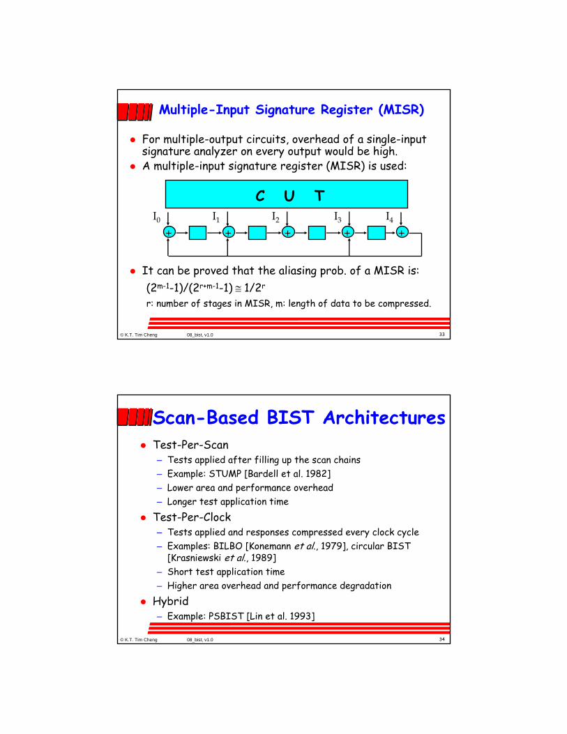
Multiple-Input Signature Register (MISR)
For multiple-output circuits, overhead of a single-input signature analyzer on every output would be high.A multiple-input signature register (MISR) is used:
It can be proved that the aliasing prob. of a MISR is: (2m-1-1)/(2r+m-1-1) ≅ 1/2r
r: number of stages in MISR, m: length of data to be compressed.
+ + + + +I0 I1 I2 I3 I4
C U T
34© K.T. Tim Cheng 08_bist, v1.0
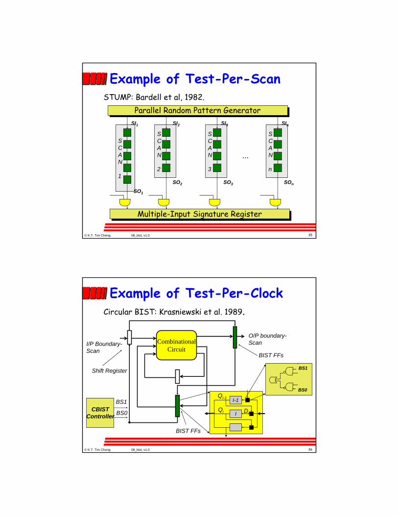
Scan-Based BIST ArchitecturesTest-Per-Scan– Tests applied after filling up the scan chains– Example: STUMP [Bardell et al. 1982]– Lower area and performance overhead– Longer test application time
Test-Per-Clock– Tests applied and responses compressed every clock cycle– Examples: BILBO [Konemann et al., 1979], circular BIST
[Krasniewski et al., 1989]– Short test application time– Higher area overhead and performance degradation
Hybrid– Example: PSBIST [Lin et al. 1993]
35© K.T. Tim Cheng 08_bist, v1.0
Example of Test-Per-Scan
SCAN
n
SCAN
3
SCAN
2
SCAN
1
Parallel Random Pattern GeneratorParallel Random Pattern Generator
Multiple-Input Signature RegisterMultiple-Input Signature Register
SIn
SOn
SI3
SO3
SI2
SO2
SI1
SO1
...
STUMP: Bardell et al, 1982.
36© K.T. Tim Cheng 08_bist, v1.0
Example of Test-Per-ClockCircular BIST: Krasniewski et al. 1989.
I/P Boundary-Scan
Shift Register
CombinationalCircuit
O/P boundary-Scan
BIST FFs
BIST FFs
I-1
IQi Di
Qi-1
BS0
BS1
CBISTController
BS1
BS0

37© K.T. Tim Cheng 08_bist, v1.0
Example of Hybrid Architecture: PSBIST
Ref: C.-J. Lin, et al.,“ Integration of Partial Scan and Built-In Self-Test”,JETTA, 1995
PIPOM
UX
LFSR
M
I
S
R
PS
SC
combinationalor feedback-freesequential circuit
Scan chains are observed per scan but PO’s are observed per clock.Scan chains are observed per scan but PO’s are observed per clock.
38© K.T. Tim Cheng 08_bist, v1.0
General BIST Issues
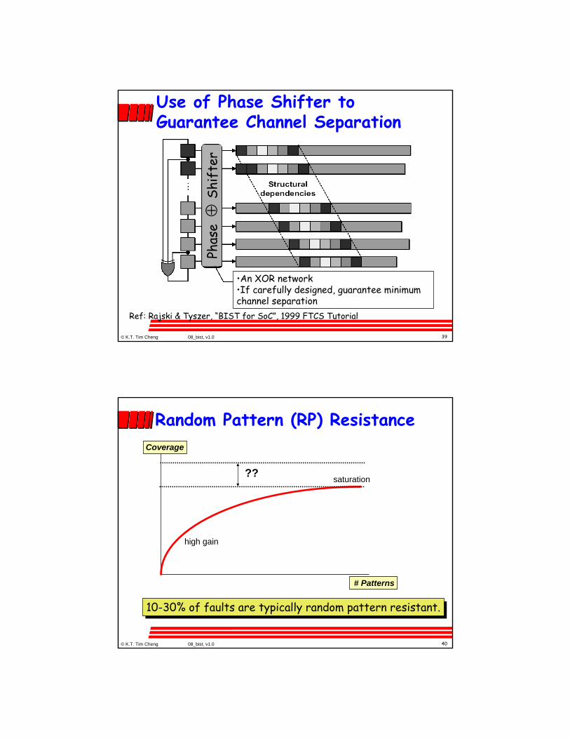
No X state propagation to observation pointsStructural dependencies for scan-based BIST– Solution: Using phase shifter
Random Pattern Resistance– Solutions: Inserting test points; Using
additional deterministic tests
39© K.T. Tim Cheng 08_bist, v1.0
Use of Phase Shifter to Guarantee Channel Separation
•An XOR network •If carefully designed, guarantee minimum channel separation
Phas
e ⊕
Shif
ter
Ref: Rajski & Tyszer, “BIST for SoC”, 1999 FTCS Tutorial
40© K.T. Tim Cheng 08_bist, v1.0
# Patterns
Random Pattern (RP) ResistanceCoverage
high gain
saturation
10-30% of faults are typically random pattern resistant.10-30% of faults are typically random pattern resistant.
??

41© K.T. Tim Cheng 08_bist, v1.0
Test Point Insertion:Inserting an Observation Point
observation
e
point
e
Region influenced byan observation point:
Circuit before addingan observation point:
Circuit after addingan observation point:
42© K.T. Tim Cheng 08_bist, v1.0
Test Point Insertion:Inserting a Control Point
control
r
e e’
e
point
G
Region influenced bya control point:
Circuit before addinga control point:
Circuit after addinga control point:
Hard to set to 1Hard to set to 1
43© K.T. Tim Cheng 08_bist, v1.0
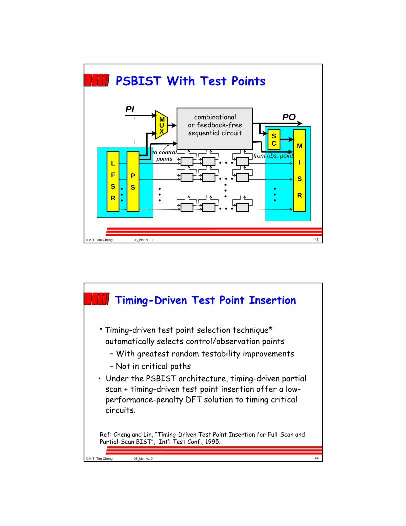
PSBIST With Test Points
PIPOM
UX
L
F
S
R
M
I
S
R
P
S
SC
combinationalor feedback-freesequential circuit
to controlpoints from obs. point
44© K.T. Tim Cheng 08_bist, v1.0
Timing-Driven Test Point Insertion
•Timing-driven test point selection technique* automatically selects control/observation points– With greatest random testability improvements– Not in critical paths
• Under the PSBIST architecture, timing-driven partial scan + timing-driven test point insertion offer a low-performance-penalty DFT solution to timing critical circuits.
Ref: Cheng and Lin, “Timing-Driven Test Point Insertion for Full-Scan and Partial-Scan BIST”, Int’l Test Conf., 1995.

45© K.T. Tim Cheng 08_bist, v1.0
Estimate of Circuit Random Pattern Testability
Detection probability of a stuck-at fault:Pd 0/s = Cs ⋅Os
Pds / 1 = (1− Cs)⋅Os
for stuck-at-0 fault at s
for stuck-at-1 fault at s
An estimate of circuit testability*:
* R. Lisanke et al, “Testability-Driven Random Test Pattern Generation”, IEEE TCAD, Nov. 1987.
U = 1F
1
pdii ∈F∑
⎛
⎝
⎜⎜⎜⎜
⎞
⎠
⎟⎟⎟⎟
46© K.T. Tim Cheng 08_bist, v1.0
COP Testability Measures (F.Brglez, 1984)
Cs: The probability of the signal having ‘1’ at signal sOs: The probability of signal s being observed at a PO
ab
X CX = Ca * CbOa = OX * Cb
ab
X CX = 1 - (1 - Ca)*(1 - Cb)Oa = OX * (1 - Cb)
a b Cb = 1 - Ca Oa = Ob
a
x
Y
CX = CY= CaOa = 1 - (1 - OX) * (1 - OY)
• Compute C’s from PI’s toward PO’s
• Compute O’s from PO’s toward PI’s
• Compute C’s from PI’s toward PO’s
• Compute O’s from PO’s toward PI’s
47© K.T. Tim Cheng 08_bist, v1.0
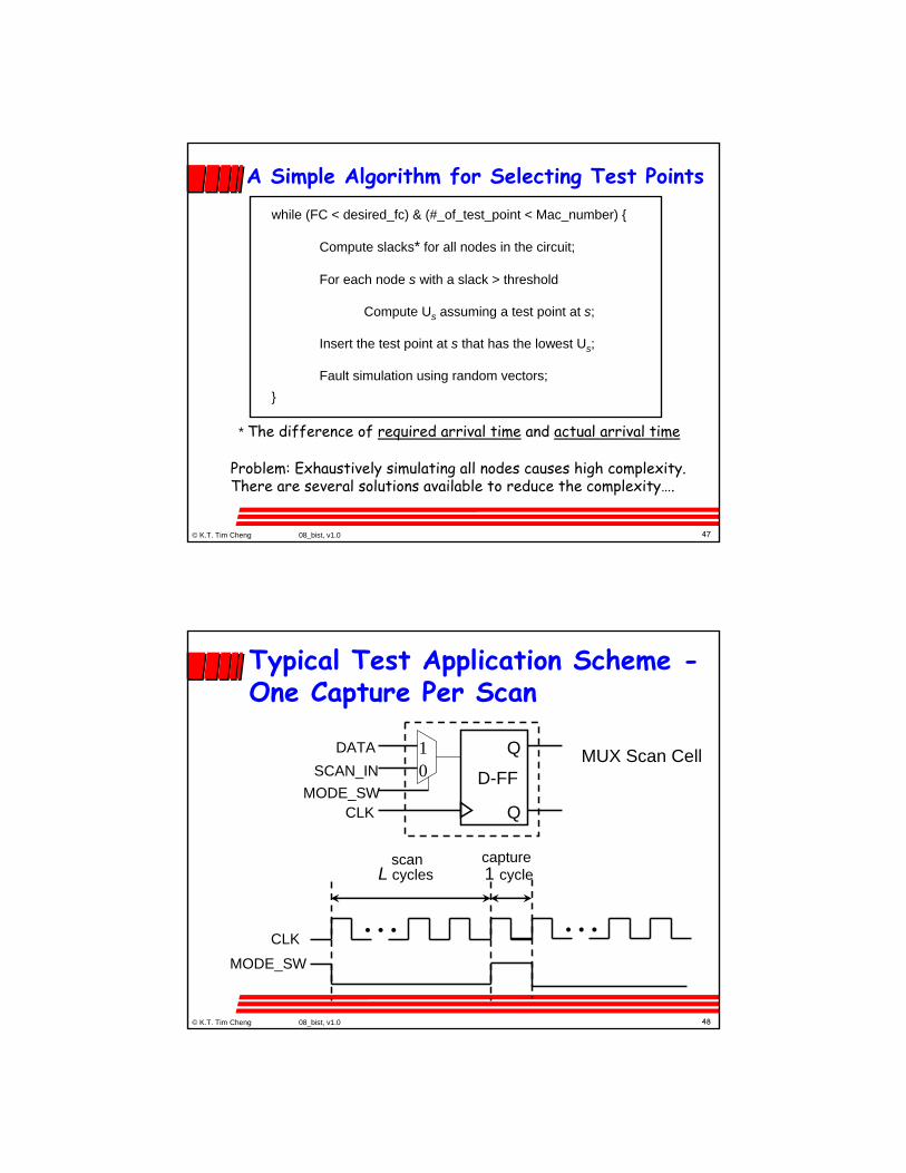
A Simple Algorithm for Selecting Test Pointswhile (FC < desired_fc) & (#_of_test_point < Mac_number) {
Compute slacks* for all nodes in the circuit;
For each node s with a slack > threshold
Compute Us assuming a test point at s;
Insert the test point at s that has the lowest Us;
Fault simulation using random vectors;}
* The difference of required arrival time and actual arrival time
Problem: Exhaustively simulating all nodes causes high complexity.There are several solutions available to reduce the complexity….
48© K.T. Tim Cheng 08_bist, v1.0
Typical Test Application Scheme -One Capture Per Scan
MUX Scan Cell01
D-FF
Q
Q
DATASCAN_IN
MODE_SWCLK
MODE_SWCLK
L cycles 1 cycle
scan capture

49© K.T. Tim Cheng 08_bist, v1.0
Scan-Based BIST Does Not Have To Be 1-Capture-Per-Scan!!
Two captures per scanscan capture
L clock cycles 2 clock cycles
MODE_SW
CLK
K captures per scank clock cycles
MODE_SW
CLK
L clock cyclesscan capture
50© K.T. Tim Cheng 08_bist, v1.0
Potential Advantages of Multiple Captures After Each Scan
ScanFF
PSI
A
CB F
Scan_in
Tests are less randomIt provides tests with different signal probability profilesAn example
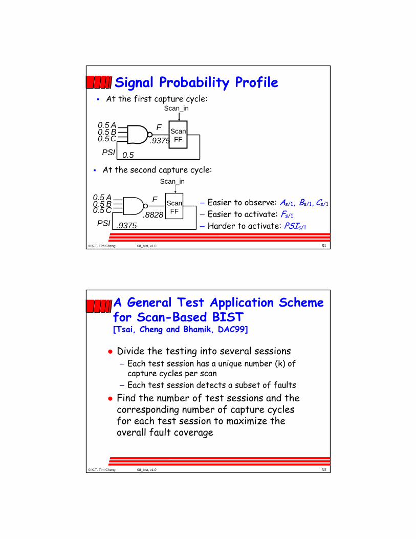
51© K.T. Tim Cheng 08_bist, v1.0
– Easier to observe: As/1, Bs/1, Cs/1
– Easier to activate: Fs/1
– Harder to activate: PSIs/1
Signal Probability Profile
ScanFF
PSI
A
C0.5F
Scan_in
0.50.5
0.5
B.9375
At the first capture cycle:
At the second capture cycle:
ScanFF
PSI
AC0.5
F
Scan_in
0.50.5 B
.9375.8828
52© K.T. Tim Cheng 08_bist, v1.0
A General Test Application Scheme for Scan-Based BIST [Tsai, Cheng and Bhamik, DAC99]
Divide the testing into several sessions– Each test session has a unique number (k) of
capture cycles per scan– Each test session detects a subset of faults
Find the number of test sessions and the corresponding number of capture cycles for each test session to maximize the overall fault coverage

53© K.T. Tim Cheng 08_bist, v1.0
Fault Coverage Curves38417
SingleMultiple
54© K.T. Tim Cheng 08_bist, v1.0
Logic BIST SummaryCircuit with logic BIST has– core logic with scan– pseudo-random pattern generator (LFSR)– response compactor: Multiple-Input Signature Register
(MISR)– BIST controller (shift counter and pattern counter)– Test points for improving random pattern testability
BIST architectures can be classified into:– Test-per-scan (such as STUMP)– Test-per-clock (such as circular BIST)– Hybrid (such as PSBIST)
Multiple captures after each scan sequence for PSBIST may improve test quality without additional hardware overhead.

55© K.T. Tim Cheng 08_bist, v1.0
System-on-Chip:Heterogeneity and Programmability
Increasing heterogeneity: More transistors doing different things!– Digital, Analog, Memory, Software, High-speed bus
Increasing programmability: Almost all SoCs have some programmable cores (Processor, DSP, FPGA)– High NRE results in fewer design starts– Domain-specific - more applications for a single design
Power/Performance
Domain specific
Programmability
General purpose Application specific
56© K.T. Tim Cheng 08_bist, v1.0
Fewer, But More Programmable Designs

57© K.T. Tim Cheng 08_bist, v1.0
Embedded-Software-Based Self-Testing For Programmable Chips
View test as an application of a programmable SOC!!View test as an application of a programmable SOC!!
Reuse of on-chip programmable components for test– Using embedded processors as general computing platform for
self-testing
Processor/DSP/FPGA cores for on-chip test generation, measurement, response analysis and even diagnosis – Self-test a processor using its instruction set for high
structural fault coverage• Bridging high-level functional test and low-level physical defects
– Use the tested processor/DSP to test buses, interfaces and other components, including analog and mixed-signal components
58© K.T. Tim Cheng 08_bist, v1.0
Embedded SW Self-Testing
BusInterface Master Wrapper
BusArbiter
Low-CostTester
On-ChipMemory
Test program
Responses
VCISignatures
DSP
VCI
IP CoreVCI
System MemoryVCI
On-chip Bus
BusInterfaceMaster Wrapper
BusInterface Target WrapperBusInterface Target Wrapper
Loading test program at low speed
Self-test at operational
speed
Unloading response
signature at low speed
CPU
Low-cost testerHigh-quality at-speed testLow test overheadNon-intrusive
Test in normal operational modeNo violation of power consumptionMore accurate speed-binning
Ref: Krstic, et al DAC’02