Out-of-plane computer-generated multicolor waveguide ...
4
Out-of-plane computer-generated multicolor waveguide holography: supplementary material Z HIQIN HUANG * , DANIEL L. MARKS, AND DAVID R. S MITH Department of Electrical and Computer Engineering, Duke University, Durham, NC 27708, USA * Corresponding author: [email protected] Published 24 January 2019 This document provides supplementary information to “Out-of-plane computer-generated multicolor waveguide holography,” https://doi.org/10.1364/OPTICA.6.000119. 1. DESIGN The multicolor holography waveguide system is designed to couple external light sources to one side of a waveguide through a grating coupler with different incident angles and then decou- ple the waves out of plane by a computer generated hologram (CGH) on the other side to reconstruct a multicolor holographic image in a range of intended angles in free space. Independent holograms are created for each of the colors and multiplexed into one metasurface binary CGH, for that light from each source propagates within the waveguide with a distinct spatial fre- quency. As shown in Figure S1a, the k-space diagram of a grating coupler illustrates how the grating period is determined once the propagation constants of the waves are obtained for the waveguide. Here, the grating equation (mk Λ = k x,inc - k r ) must be satisfied and only the -1st order diffracted waves propagate to the hologram. The k-diagram in Figure S1b shows that if the incident beams accidentally illuminate the hologram directly, only the zero-order reflection of the hologram occurs, but at angles outside of the reconstruction and collection region (gray area). The k-diagram of the hologram decoupler in Figure S1c shows that only the -1st order diffraction participates in forming the holographic images. The generated holographic image are reconstructed over an intended range of angles and collected by an imaging system that consists of a collector lens and a digital camera. Figure S1d illustrates the multilayer system, showing a grat- ing coupler and a CGH decoupler with waveguide modes prop- agating in the waveguide region. In a multicolor holographic design, the period is set to be 280 nm, which requires the inci- dent angles are -52.7 ◦ (red), -24.1 ◦ (green) and -5.8 ◦ (blue). The object in the example is taken as a letter combination with a red “R” followed with a green “G” and a blue “B” . Here, the decoupling angle range in the x-direction is set to be from -35 ◦ to -45 ◦ , while it is set to be from -5 ◦ to 5 ◦ in the y-direction. A theoretical multicolor holographic image of “RGB” is recon- structed in the designed region. Note that the image seems to be a mirror of the object in the 2D profile, while in the actual 3D experiment it is just as the object. As shown, only the letters with the correct color combination locate in the intended range of angles; letters corresponding to other diffracted orders lies outside of the collection region. To obtain an optimized intensity distribution for the recon- structed holographic image, we follow the design process indi- cated in the flowchart shown in Figure S2a[1, 2]. We start with a desired color image that is to serve as the object. For the present work, the images have three colors that are spatially distributed. We then separate the image into three color planes, each result- ing in a black and white image corresponding to one of the three color channels. We then map each pixel on each color plane to a decoupling angle located in a certain range. The minimum and maximum of the decoupling angles are chosen such that the Fourier components for each color are disjoint, as shown in Figure S2b and in the example of multicolor RGB letters in Figure S2c. It should be noted that different color planes are combined into a single Fourier space. Then a GS-based holo- gram generation process is performed[3], as labeled with dashed lines in the Figure S2a. A random phase is superimposed on the desired amplitude to form a complex field and then impose a fast Fourier transform (FFT) to the spectrum domain. Apply a constraint to the generated hologram which requires that the hologram must be a binary hologram due to the limitation of the current fabrication, in which the CGH part metasurface would be either partially etched or not. A reconstruction algorithm is used to check if the holographic image generated by the CGH is acceptable or not when compared to the original object. If not, the modified hologram is converted back to the spatial domain by performing an inverse fast Fourier transform (iFFT). Apply a constraint in the spatial field to enforce the amplitude in the far field connecting to the decoupling angles. The new field is regarded as the initial field for the next iteration. The smallest
Transcript of Out-of-plane computer-generated multicolor waveguide ...
Out-of-plane computer-generated multicolorwaveguide holography: supplementary materialZHIQIN HUANG*, DANIEL L. MARKS, AND DAVID R. SMITHDepartment of Electrical and Computer Engineering, Duke University, Durham, NC 27708, USA*Corresponding author: [email protected]
Published 24 January 2019
This document provides supplementary information to “Out-of-plane computer-generated multicolor waveguide holography,” https://doi.org/10.1364/OPTICA.6.000119.
1. DESIGN
The multicolor holography waveguide system is designed tocouple external light sources to one side of a waveguide througha grating coupler with different incident angles and then decou-ple the waves out of plane by a computer generated hologram(CGH) on the other side to reconstruct a multicolor holographicimage in a range of intended angles in free space. Independentholograms are created for each of the colors and multiplexed intoone metasurface binary CGH, for that light from each sourcepropagates within the waveguide with a distinct spatial fre-quency.
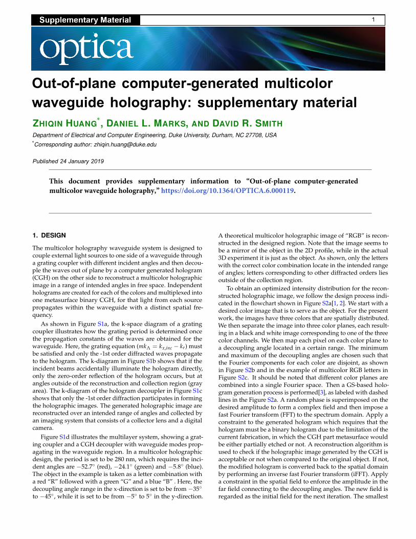
As shown in Figure S1a, the k-space diagram of a gratingcoupler illustrates how the grating period is determined oncethe propagation constants of the waves are obtained for thewaveguide. Here, the grating equation (mkΛ = kx,inc − kr) mustbe satisfied and only the -1st order diffracted waves propagateto the hologram. The k-diagram in Figure S1b shows that if theincident beams accidentally illuminate the hologram directly,only the zero-order reflection of the hologram occurs, but atangles outside of the reconstruction and collection region (grayarea). The k-diagram of the hologram decoupler in Figure S1cshows that only the -1st order diffraction participates in formingthe holographic images. The generated holographic image arereconstructed over an intended range of angles and collected byan imaging system that consists of a collector lens and a digitalcamera.
Figure S1d illustrates the multilayer system, showing a grat-ing coupler and a CGH decoupler with waveguide modes prop-agating in the waveguide region. In a multicolor holographicdesign, the period is set to be 280 nm, which requires the inci-dent angles are −52.7◦ (red), −24.1◦ (green) and −5.8◦ (blue).The object in the example is taken as a letter combination witha red “R” followed with a green “G” and a blue “B” . Here, thedecoupling angle range in the x-direction is set to be from −35◦
to −45◦, while it is set to be from −5◦ to 5◦ in the y-direction.
A theoretical multicolor holographic image of “RGB” is recon-structed in the designed region. Note that the image seems tobe a mirror of the object in the 2D profile, while in the actual3D experiment it is just as the object. As shown, only the letterswith the correct color combination locate in the intended rangeof angles; letters corresponding to other diffracted orders liesoutside of the collection region.
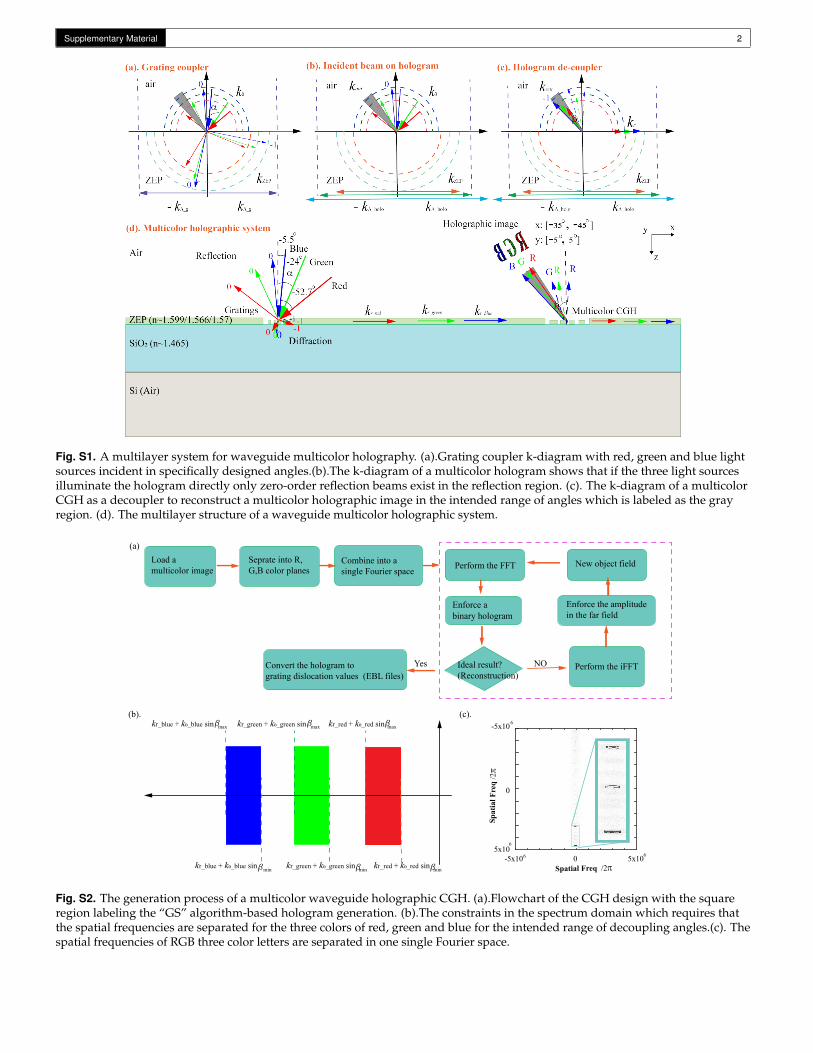
To obtain an optimized intensity distribution for the recon-structed holographic image, we follow the design process indi-cated in the flowchart shown in Figure S2a[1, 2]. We start with adesired color image that is to serve as the object. For the presentwork, the images have three colors that are spatially distributed.We then separate the image into three color planes, each result-ing in a black and white image corresponding to one of the threecolor channels. We then map each pixel on each color plane toa decoupling angle located in a certain range. The minimumand maximum of the decoupling angles are chosen such thatthe Fourier components for each color are disjoint, as shownin Figure S2b and in the example of multicolor RGB letters inFigure S2c. It should be noted that different color planes arecombined into a single Fourier space. Then a GS-based holo-gram generation process is performed[3], as labeled with dashedlines in the Figure S2a. A random phase is superimposed on thedesired amplitude to form a complex field and then impose afast Fourier transform (FFT) to the spectrum domain. Apply aconstraint to the generated hologram which requires that thehologram must be a binary hologram due to the limitation of thecurrent fabrication, in which the CGH part metasurface wouldbe either partially etched or not. A reconstruction algorithm isused to check if the holographic image generated by the CGH isacceptable or not when compared to the original object. If not,the modified hologram is converted back to the spatial domainby performing an inverse fast Fourier transform (iFFT). Applya constraint in the spatial field to enforce the amplitude in thefar field connecting to the decoupling angles. The new field isregarded as the initial field for the next iteration. The smallest
Supplementary Material 2
Fig. S1. A multilayer system for waveguide multicolor holography. (a).Grating coupler k-diagram with red, green and blue lightsources incident in specifically designed angles.(b).The k-diagram of a multicolor hologram shows that if the three light sourcesilluminate the hologram directly only zero-order reflection beams exist in the reflection region. (c). The k-diagram of a multicolorCGH as a decoupler to reconstruct a multicolor holographic image in the intended range of angles which is labeled as the grayregion. (d). The multilayer structure of a waveguide multicolor holographic system.
(b).
(a)
kr_blue + k0_blue sin bmax kr_green + k0_green sin maxb kr_red + k0_red sin maxb
kr_blue + k0_blue sin b kr_green + k0_green sin b kr_red + k0_red sin bmin min min
(c).
Spat
ial F
req
/2π
Spatial Freq /2π
5x10⁶
-5x10⁶
0
0 5x10⁶-5x10⁶
Load a multicolor image Perform the FFT
Enforce the amplitude in the far field
Perform the iFFT
Enforce abinary hologram
Convert the hologram tograting dislocation values (EBL files)
Ideal result?(Reconstruction)
NOYes
Seprate into R,G,B color planes
Combine into asingle Fourier space
New object field
Fig. S2. The generation process of a multicolor waveguide holographic CGH. (a).Flowchart of the CGH design with the squareregion labeling the “GS” algorithm-based hologram generation. (b).The constraints in the spectrum domain which requires thatthe spatial frequencies are separated for the three colors of red, green and blue for the intended range of decoupling angles.(c). Thespatial frequencies of RGB three color letters are separated in one single Fourier space.

Supplementary Material 3
(c) (d)
(a)
SiO2
Si substrate
(b)
SiO2
Si substrate
ZEP
0
60 nm
2 µm
2 µm
0
500 nm
Hologram design (µm)
Fig. S3. Fabrication processes of waveguide holographic sam-ples. (a). the cladding layer of SiO2 is grown by PECVD. (b).the grating and hologram patterns of metasurface core layerare formed through EBL. (c).SEM image of a part of a fabri-cated hologram. (d).AFM images of the fabricated grating.
feature size designed in the hologram is set to be 100 nm andthe periods for the generated holograms for different colors arequite small (less than 300 nm), which makes the reconstructedhologram image only have the -1st diffraction order solution,as shown in Figure S1c. Therefore, no twin images would begenerated as happens to other hologram generation methodssuch as in Gabor holograms [4].
2. FABRICATION
To validate the designed multicolor waveguide holographic sys-tem, different samples have been fabricated utilizing nanofabri-cation techniques. The main fabrication process of the waveg-uide holographic samples includes two steps of plasma en-hanced chemical vapor deposition (PECVD) and electron-beamlithography (EBL), as shown in Figure S3.
First, a 2 µm waveguide cladding layer of SiO2 is depositedon silicon substrates through PECVD (Advanced Vacuum Vision310) with a deposition temperature of 250◦C. Then the gratingand hologram structures are transferred to the metasurface layerutilizing EBL (Elionix ELS-7500 EX) with an electron beam re-sist of ZEP-520A, as shown in Figure S3 a and b. The designedthickness of metasurface layer is 300 nm, which is controlled bythe dilution ratio with anisole (Sigma-Aldrich, 99.7 %) and thespin-coating speed. The depth of the etched structures is around60 nm, which is controlled by the EBL dose time and the developtime in O-Xylene (Sigma-Aldrich, > 98%). The metasurfacethickness is measured by a film thickness measurement reflec-tometer (Nanometrics 210). The overall size of the hologram inthe metasurface layer is designed to be 300 µm × 300µm (one ofthe available field sizes for the EBL system) and the smallest fea-ture size is set to be 100 nm. One of the designed grating periodsis set to be 280 nm with a fill fraction of 0.5. The structure detailsof the fabricated holograms and gratings were checked with anSEM (Scanning Electron Microscope, FEI XL30 SEM-FEG) andAFM (Atomic Force Microscope, Digital Instruments Dimension3100), as shown in Figure S3 c and d. The optical properties ofthe PECVD grown SiO2 were characterized by an ellipsometerVASE (Variable Angle Spectroscopic Ellipsometer, J. A. WoollamM-88), and the result could be found in Figure S4 a and b.
A commercial electron-beam resist of ZEP (ZEP520A, ZEONCorporation, Japan) is selected to make the metasurface layerfor the following reasons. First, the refractive index of the meta-
500 600 700 500 600 700Wavelength λ (nm)
Ext
inct
ion
Coe
ffic
ient
κ
Ref
ract
ive
inde
x n
1.45
1.46
1.47
1.48
0.008
0.004
0
(a) (b)
1.58
1.57
1.56Ref
ract
ive
inde
x n
(c) (d)
500 600 700 500 600 700
0.001
0 0
Ext
inct
ion
Coe
ffic
ient
κ
Wavelength λ (nm)
Wavelength λ (nm)Wavelength λ (nm)
Fig. S4. Measured optical properties of SiO2 and ZEP. (a) re-fractive index and (b) extinction coefficient of SiO2; (c) refrac-tive index and (d) extinction coefficient of ZEP.
surface ZEP is larger than that of air and SiO2 , which makesa perfect waveguide structure. Compared with other potentialresist candidates having larger refractive index, such as siliconnitride (SiNx), the extinction coefficient of ZEP is quite small,which is crucial to efficiently propagate light in the waveguideover a longer distance. The extinction properties have been ver-ified by VASE measurements, as shown in Figure S4 c and d.Furthermore, compared to other commonly used electron-beamresists such as different kinds of PMMA(Polymethyl methacry-late), the resolution and contrast of ZEP is much higher and itsetch resistance is better, which makes it a good candidate forstructure modeling. Note that both the gratings coupler and theCGH decoupler are formed in the metasurface layer of ZEP.
3. CHARACTERIZATION
L1
L2
F1S1: A metasurface-based waveguide holographic sample
L1, L2, L3: Plane-convex lenses
F1, F2, F3: Intensity filters
532 nm Laser
635 nm laser
450 nm Laser
L3
F2
F3
S1
CCDCamera
PC Control
Fig. S5. An optical characterization system.
An optical system was built to characterize the performance offabricated samples and check if the designed holographic imagescould be reconstructed in the intended range of angles,as shown

Supplementary Material 4
in Figure S5. The light sources consist of three semiconductorlaser modules (Thorlabs, Inc.) with operational wavelengthsat 635 (red), 532 (green) and 450 nm (blue). A combination oftwo lenses (L1 and L2) with the focal lengths of 25 mm and 50mm are used in each color branch to collimate the beam andadjust the spot size of each light source, while the intensityfilters are used to balance the beam power from each source for abetter demonstration. The incident angles for three light sourcesare built to be −52.7◦ (red), −24.2◦ (green) and −5.8◦ (blue), asdesigned with the grating coupler period of 280 nm. For a single-color hologram design, only one light source is needed. For amulticolor design, all the three sources are used to illuminate thegrating coupler on a metasurface sample at designed incidentangles and a holographic image will be generated at the intendedrange of angles. The generated holographic images could beobserved directly. And it could be collected by an imagingsystem as well. A collector lens (L3) with the focal length of200 mm is used to focus the out-coupled holographic image.Then the holographic image is collected with a CCD commercialdigital camera (Nikon D90) with a focal length of 130 mm lens.
REFERENCES
1. M. Li, J. Bengtsson, M. Hagberg, A. Larsson, andT. Suhara, “Off-plane computer-generated waveguide holo-gram,” IEEE J. Sel. Top. Quantum Electron. 2, 226–235 (1996).
2. J.-P. L. Ting-Chung Poon, Introduction to Modern Digital Holography With Matlab (Cambridge University Press, 2014).
3. R. W. Gerchberg and W. O. Saxton, “A practical algorithm for the determination of phase from image and diffraction plane pictures,” Optik (Stuttg). 35, 237–246 (1972).
4. J. W. Goodman, Introduction to Fourier Optics (Roberts and Company Publishers, 2008).