Oscillators, Phase Locked Loops · • Used in Phase Locked Loops (Loops (PLLs – chapter 15)...
30
Oscillators, Phase Locked Loops Oscillators, Phase Locked Loops Tuesday, March 29th, 9:15 – 11:30 Snorre Aunet ([email protected]) Nanoelectronics group Department of Informatics University of Oslo
Transcript of Oscillators, Phase Locked Loops · • Used in Phase Locked Loops (Loops (PLLs – chapter 15)...
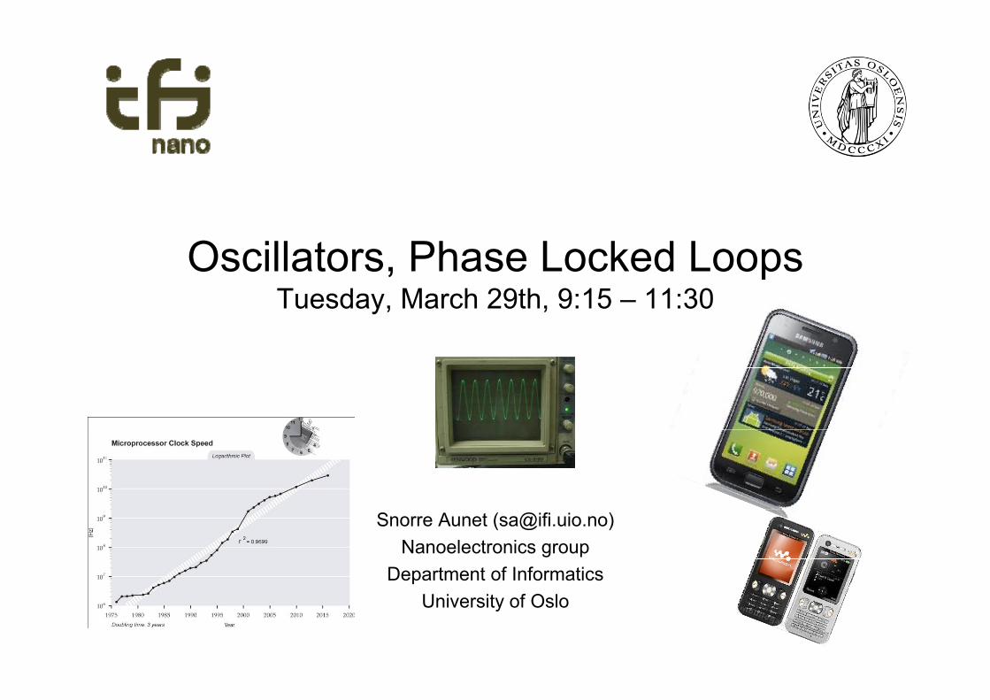
Oscillators, Phase Locked LoopsOscillators, Phase Locked LoopsTuesday, March 29th, 9:15 – 11:30
Snorre Aunet ([email protected])Nanoelectronics group
Department of InformaticsUniversity of Oslo
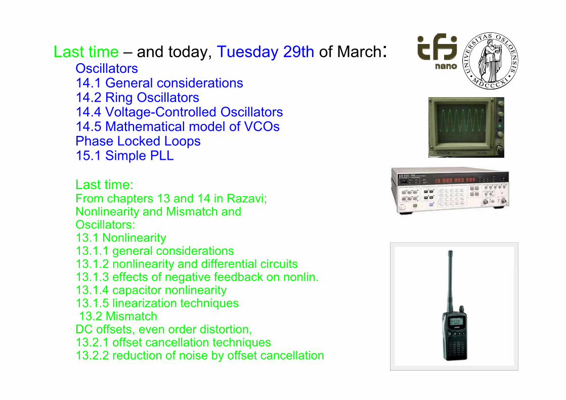
Last time – and today, Tuesday 29th of March:O ill tOscillators14.1 General considerations14.2 Ring Oscillators14 4 V lt C t ll d O ill t14.4 Voltage-Controlled Oscillators14.5 Mathematical model of VCOsPhase Locked Loops15 1 Simple PLL15.1 Simple PLL
Last time:From chapters 13 and 14 in Razavi;From chapters 13 and 14 in Razavi;Nonlinearity and Mismatch andOscillators:13.1 Nonlinearity13.1.1 general considerations13.1.2 nonlinearity and differential circuits13.1.3 effects of negative feedback on nonlin.13 1 4 capacitor nonlinearity13.1.4 capacitor nonlinearity13.1.5 linearization techniques13.2 MismatchDC offsets, even order distortion, 13.2.1 offset cancellation techniques13.2.2 reduction of noise by offset cancellation
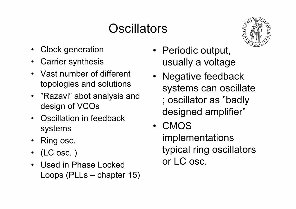
Oscillators• Periodic output, • Clock generation
usually a voltage• Negative feedback
• Carrier synthesis• Vast number of different
t l i d l tig
systems can oscillate; oscillator as ”badly
topologies and solutions• ”Razavi” abot analysis and
design of VCOs; ydesigned amplifier”
• CMOS
design of VCOs• Oscillation in feedback
systems CMOS implementationstypical ring oscillators
systems• Ring osc. • (LC osc ) typical ring oscillators
or LC osc.• (LC osc. )• Used in Phase Locked
Loops (PLLs – chapter 15)Loops (PLLs – chapter 15)
Oscillators
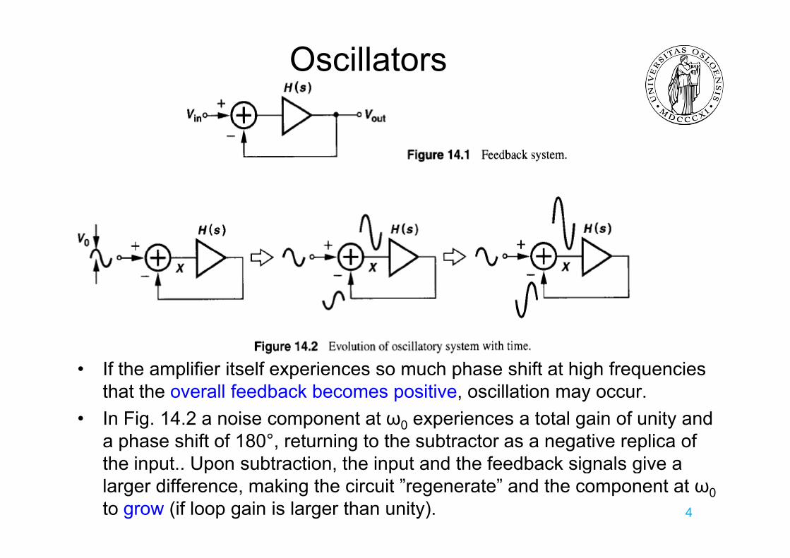
• If the amplifier itself experiences so much phase shift at high frequenciesthat the overall feedback becomes positive, oscillation may occur.
• In Fig. 14.2 a noise component at ω0 experiences a total gain of unity and a phase shift of 180°, returning to the subtractor as a negative replica ofthe input.. Upon subtraction, the input and the feedback signals give athe input.. Upon subtraction, the input and the feedback signals give a larger difference, making the circuit ”regenerate” and the component at ω0to grow (if loop gain is larger than unity). 4
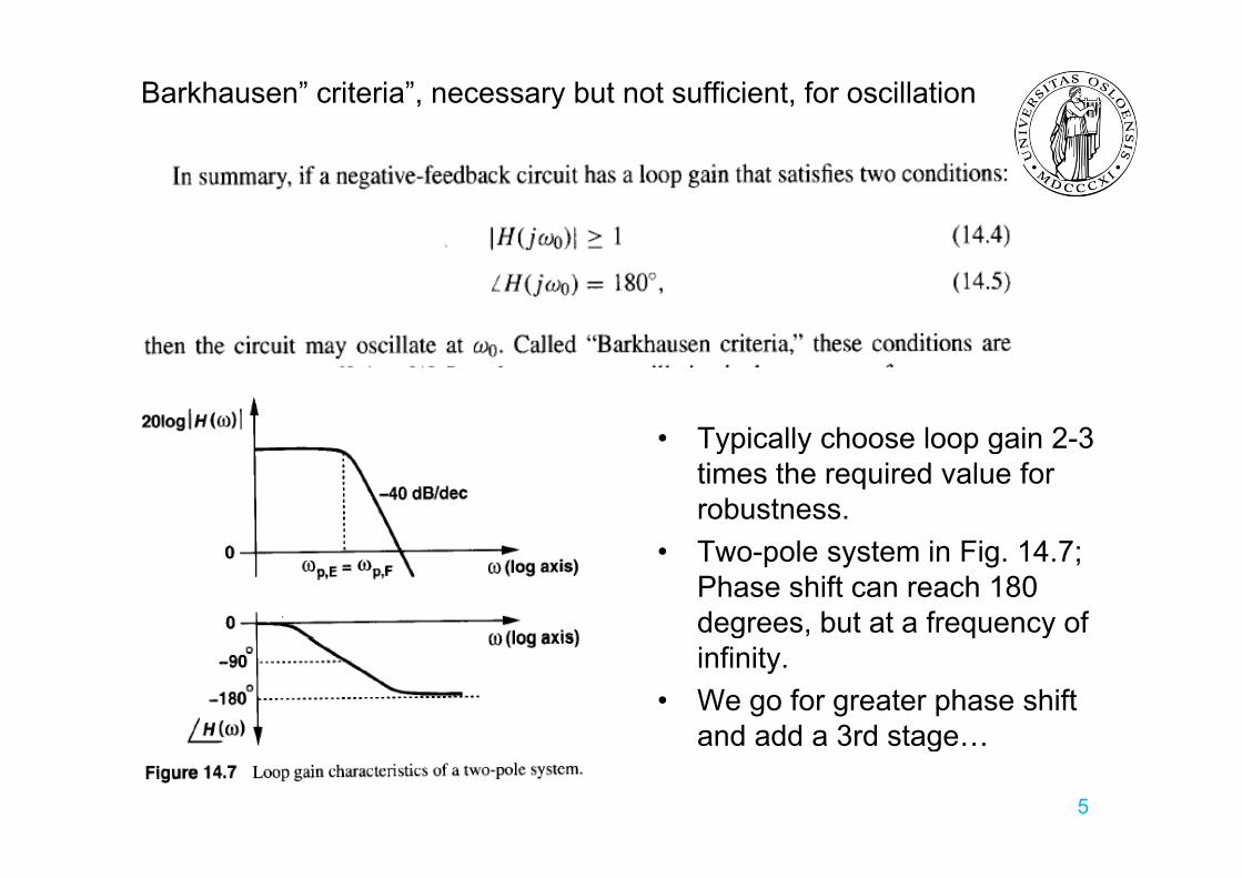
Barkhausen” criteria”, necessary but not sufficient, for oscillation
• Typically choose loop gain 2 3• Typically choose loop gain 2-3 times the required value for robustness.
• Two-pole system in Fig. 14.7; Phase shift can reach 180 degrees, but at a frequency ofg yinfinity.
• We go for greater phase shiftand add a 3rd stageand add a 3rd stage…
5
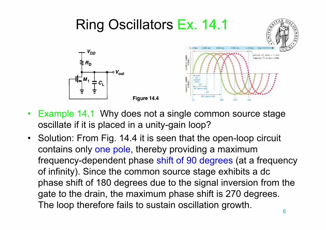
Ring Oscillators Ex. 14.1
• Example 14 1 Why does not a single common source stageExample 14.1 Why does not a single common source stage oscillate if it is placed in a unity-gain loop?
• Solution: From Fig. 14.4 it is seen that the open-loop circuitSolution: From Fig. 14.4 it is seen that the open loop circuitcontains only one pole, thereby providing a maximumfrequency-dependent phase shift of 90 degrees (at a frequencyof infinity). Since the common source stage exhibits a dcphase shift of 180 degrees due to the signal inversion from thegate to the drain the maximum phase shift is 270 degreesgate to the drain, the maximum phase shift is 270 degrees. The loop therefore fails to sustain oscillation growth.
6
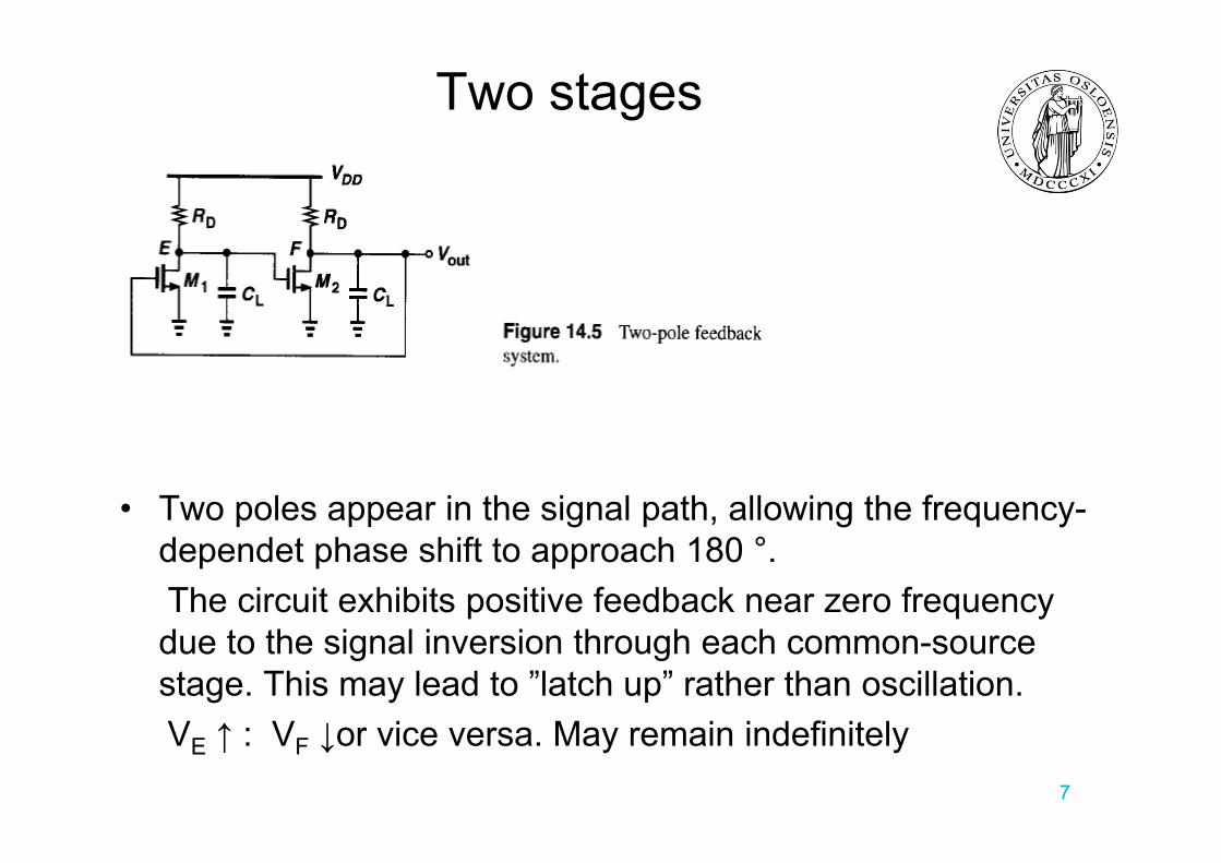
Two stages
• Two poles appear in the signal path, allowing the frequency-dependet phase shift to approach 180 °. The circuit exhibits positive feedback near zero frequencydue to the signal inversion through each common-sourcestage. This may lead to ”latch up” rather than oscillation.V ↑ V ↓ i M i i d fi it lVE ↑ : VF ↓or vice versa. May remain indefinitely
7
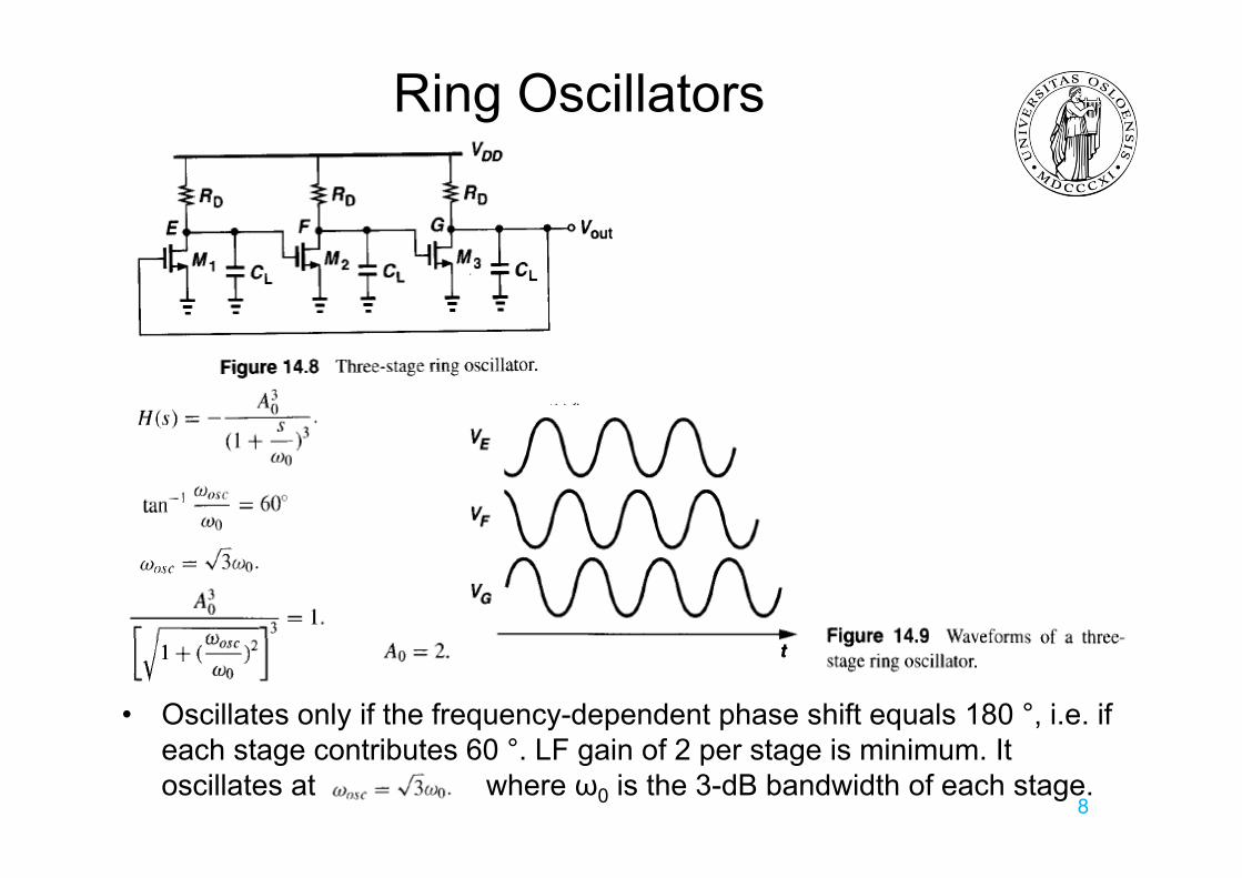
Ring Oscillators
• Oscillates only if the frequency-dependent phase shift equals 180 °, i.e. ifeach stage contributes 60 °. LF gain of 2 per stage is minimum. It oscillates at where ω0 is the 3-dB bandwidth of each stage.
8
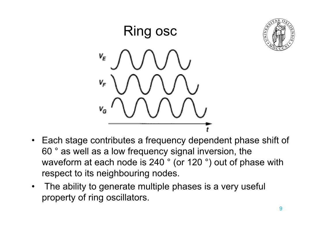
Ring oscg
• Each stage contributes a frequency dependent phase shift of• Each stage contributes a frequency dependent phase shift of60 ° as well as a low frequency signal inversion, thewaveform at each node is 240 ° (or 120 °) out of phase withwaveform at each node is 240 (or 120 ) out of phase withrespect to its neighbouring nodes.
• The ability to generate multiple phases is a very usefuly g p p yproperty of ring oscillators.
9
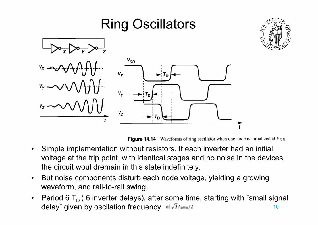
Ring Oscillators
• Simple implementation without resistors. If each inverter had an initial voltage at the trip point, with identical stages and no noise in the devices, the circuit woul dremain in this state indefinitely.
• But noise components disturb each node voltage, yielding a growingwaveform, and rail-to-rail swing.waveform, and rail to rail swing.
• Period 6 TD ( 6 inverter delays), after some time, starting with ”small signal delay” given by oscilation frequency 10
Voltage controlled oscillators (VCOs)
• A VCO has it’s oscillation frequency controlled by a voltage input.q y y g p• The frequency of oscillation is varied by the applied DC voltage, while
modulating signals may also be fed into the VCO to cause frequency modulation (FM) or phase modulation (PM); a VCO with digital pulsemodulation (FM) or phase modulation (PM); a VCO with digital pulse output may similarly have its repetition rate (FSK, PSK) or pulse widthmodulated (PWM).
• Harmonic oscillators generate a sinus waveform.• Relaxation oscillators can generate a sawtooth or triangular waveform.• (from Wikipedia)• (from Wikipedia)
11
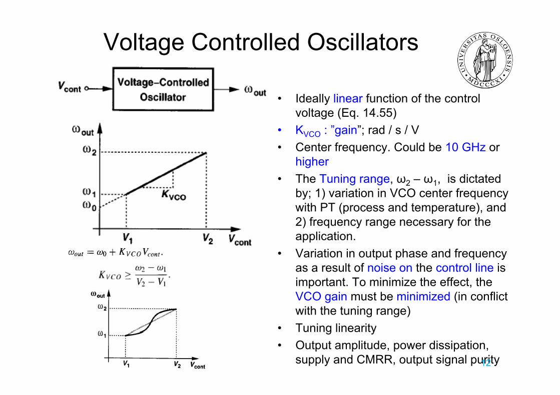
Voltage Controlled Oscillators
• Ideally linear function of the controlvoltage (Eq. 14.55)
• KVCO : ”gain”; rad / s / V• Center frequency. Could be 10 GHz or q y
higher• The Tuning range, ω2 – ω1, is dictated
by; 1) variation in VCO center frequencyy; ) q ywith PT (process and temperature), and 2) frequency range necessary for theapplication.pp
• Variation in output phase and frequencyas a result of noise on the control line is important. To minimize the effect, thep ,VCO gain must be minimized (in conflictwith the tuning range)
• Tuning linearityu g ea y• Output amplitude, power dissipation,
supply and CMRR, output signal purity12
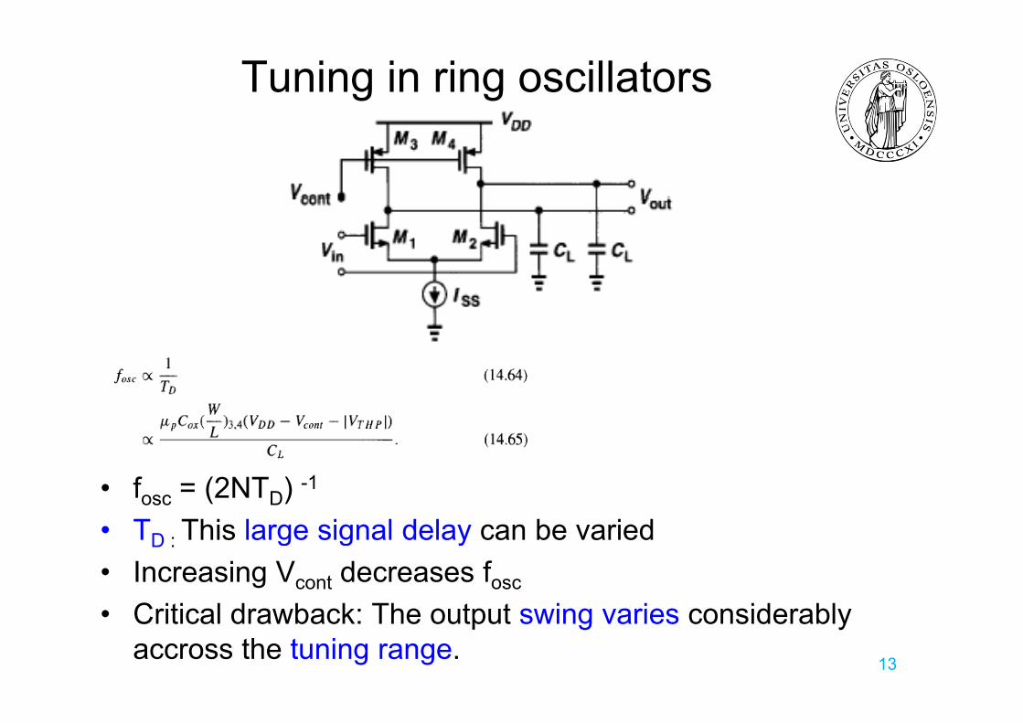
Tuning in ring oscillators
• fosc = (2NTD) -1
T This large signal delay can be varied• TD : This large signal delay can be varied• Increasing Vcont decreases fosc
C iti l d b k Th t t i i id bl• Critical drawback: The output swing varies considerablyaccross the tuning range. 13
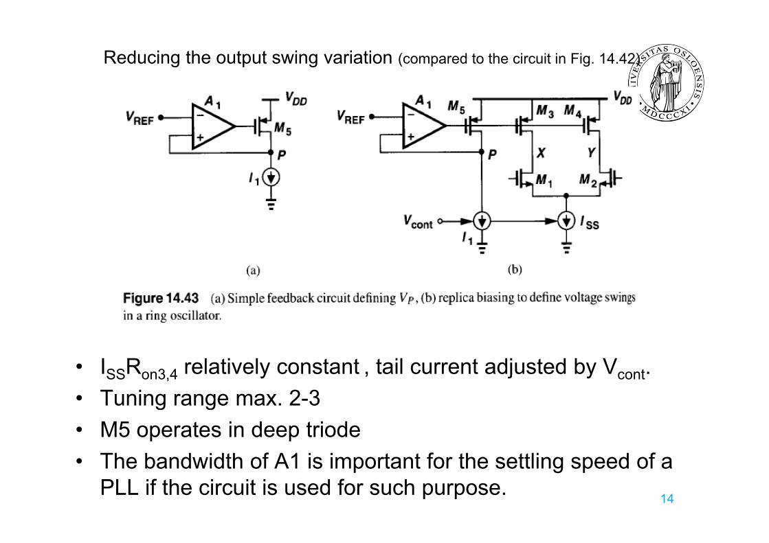
Reducing the output swing variation (compared to the circuit in Fig. 14.42)
• ISSRon3,4 relatively constant , tail current adjusted by Vcont.Tuning range max 2 3• Tuning range max. 2-3
• M5 operates in deep triodeTh b d idth f A1 i i t t f th ttli d f• The bandwidth of A1 is important for the settling speed of a PLL if the circuit is used for such purpose. 14
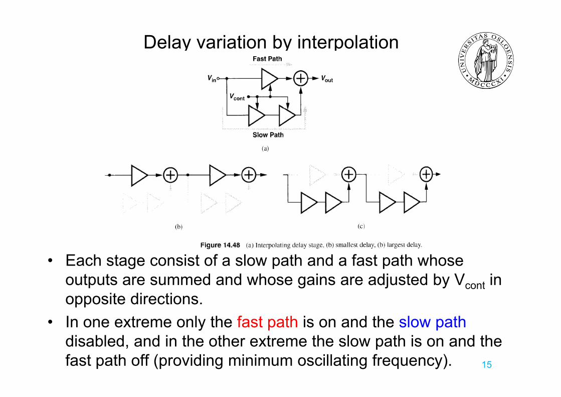
Delay variation by interpolation
• Each stage consist of a slow path and a fast path whoseoutputs are summed and whose gains are adjusted by Vcont in contopposite directions.
• In one extreme only the fast path is on and the slow pathdisabled, and in the other extreme the slow path is on and thefast path off (providing minimum oscillating frequency). 15
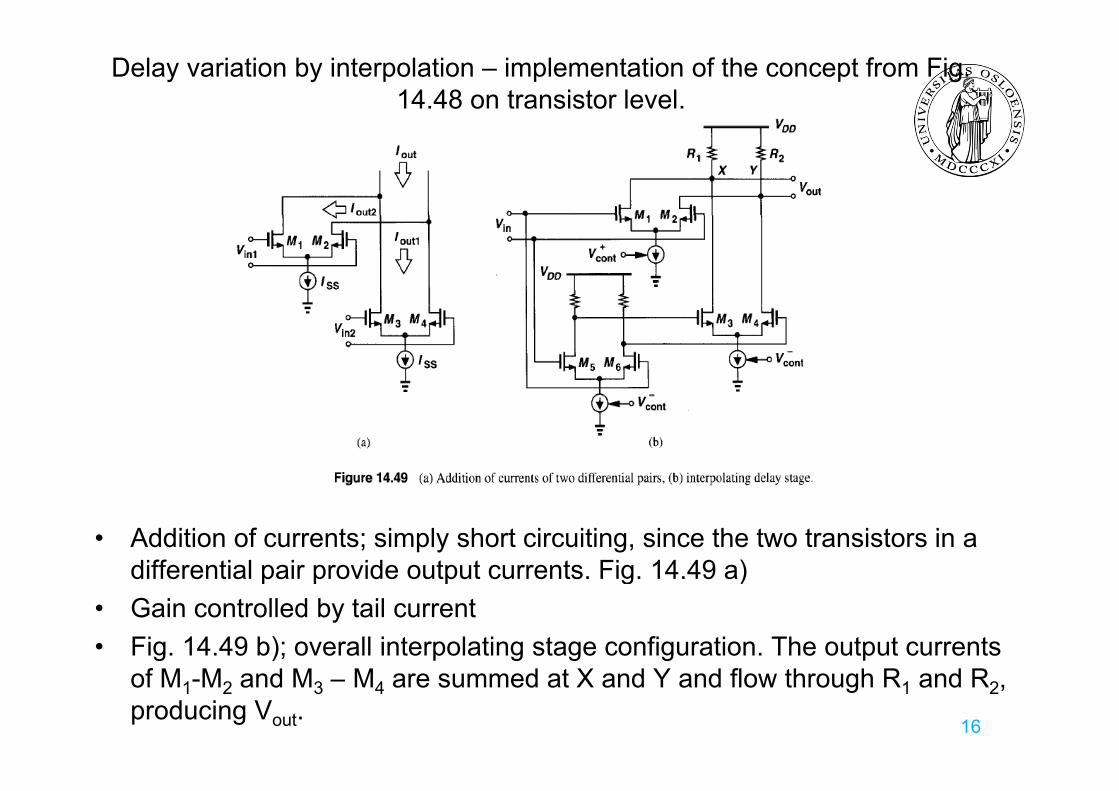
Delay variation by interpolation – implementation of the concept from Fig. 14.48 on transistor level.
• Addition of currents; simply short circuiting, since the two transistors in a differential pair provide output currents Fig 14 49 a)differential pair provide output currents. Fig. 14.49 a)
• Gain controlled by tail current• Fig. 14.49 b); overall interpolating stage configuration. The output currents
of M1-M2 and M3 – M4 are summed at X and Y and flow through R1 and R2, producing Vout. 16
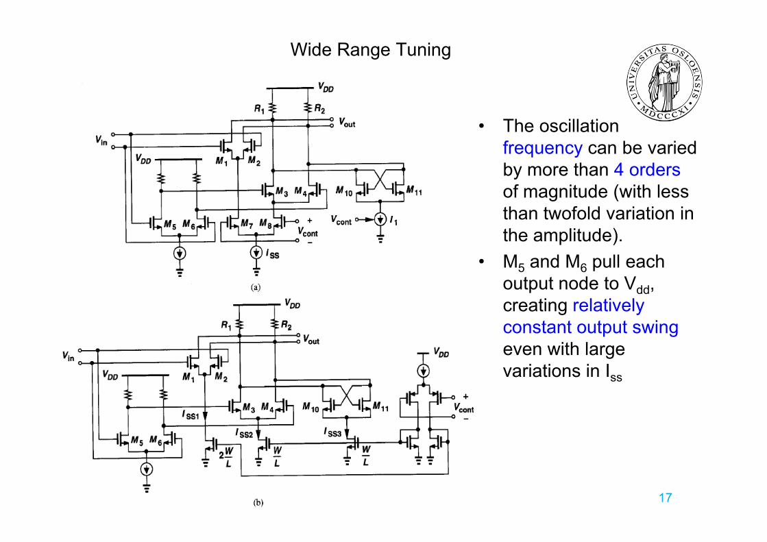
Wide Range Tuning
• The oscillationfrequency can be variedfrequency can be variedby more than 4 ordersof magnitude (with less th t f ld i ti ithan twofold variation in the amplitude).
• M5 and M6 pull each5 6 poutput node to Vdd, creating relativelyconstant output swingconstant output swing even with large variations in Iss
17
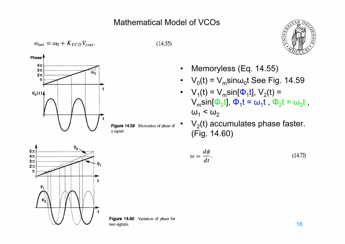
Mathematical Model of VCOs
M l (E 14 55)• Memoryless (Eq. 14.55)• V0(t) = Vmsinω0t See Fig. 14.59• V1(t) = Vmsin[Φ1t], V2(t) =V1(t) Vmsin[Φ1t], V2(t)
Vmsin[Φ2t], Φ1t = ω1t , Φ2t = ω2t , ω1 < ω2
V (t) acc m lates phase faster• V2(t) accumulates phase faster. (Fig. 14.60)
18
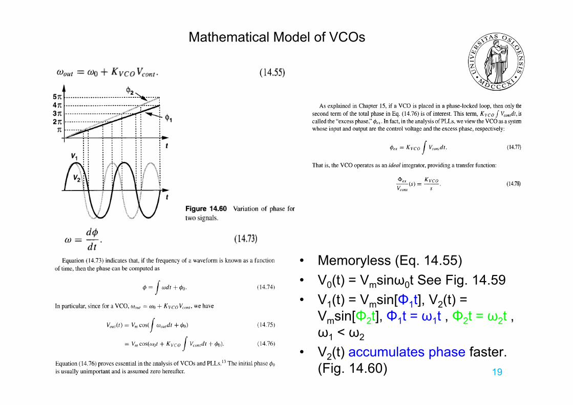
Mathematical Model of VCOs
• Memoryless (Eq. 14.55)• V0(t) = Vmsinω0t See Fig. 14.59
V ( ) V i [Φ ] V ( )• V1(t) = Vmsin[Φ1t], V2(t) = Vmsin[Φ2t], Φ1t = ω1t , Φ2t = ω2t , ω1 < ω2
• V2(t) accumulates phase faster. (Fig. 14.60) 19
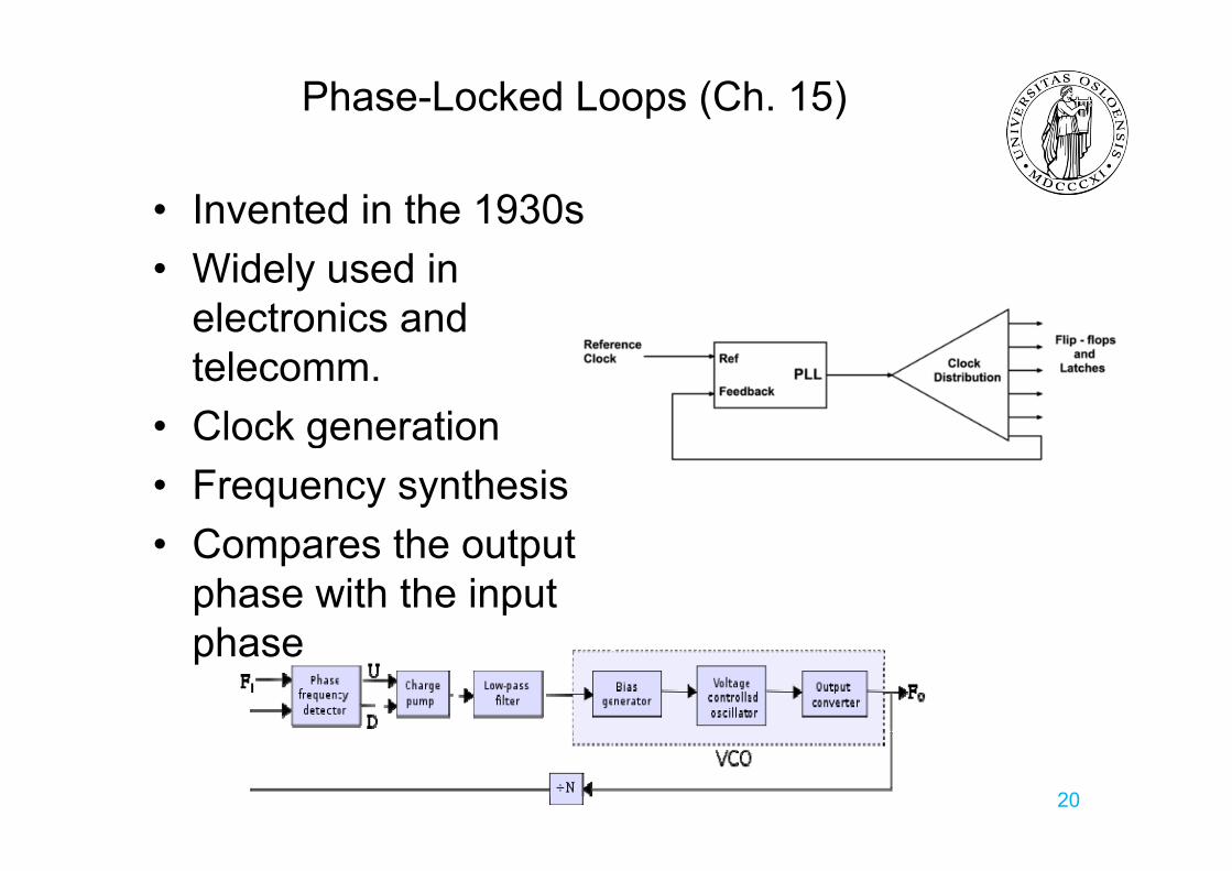
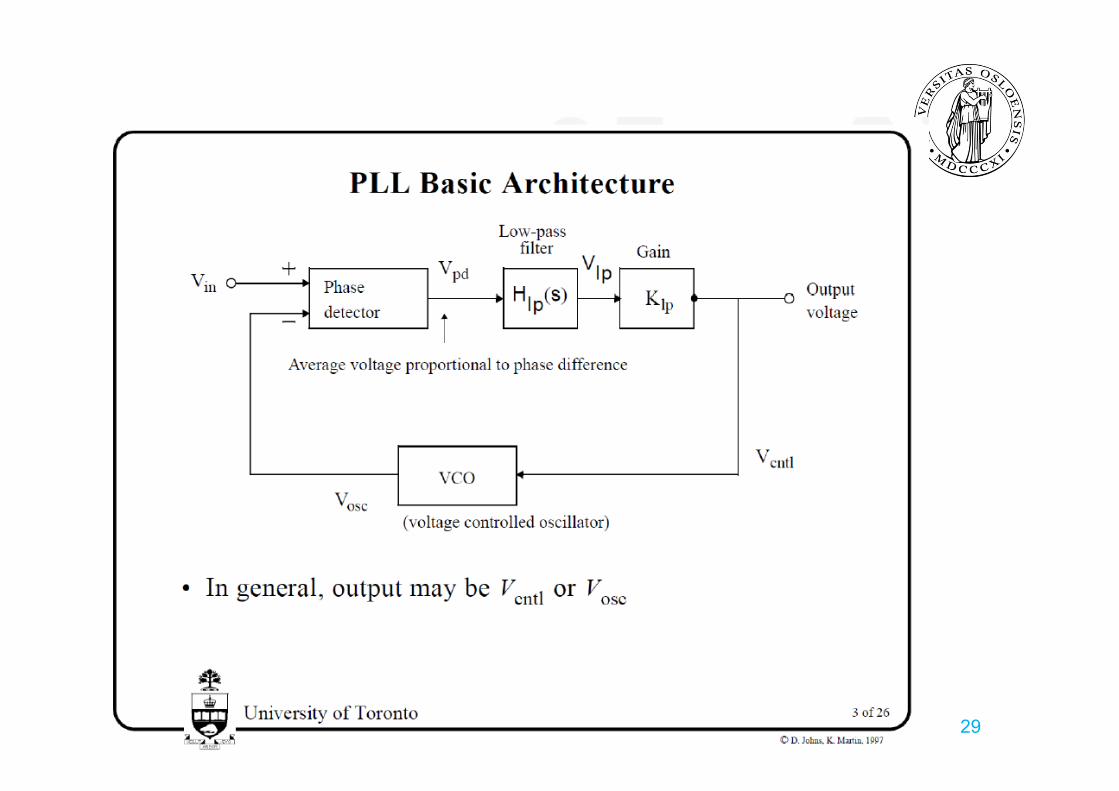
Phase-Locked Loops (Ch. 15)
• Invented in the 1930s• Widely used in
electronics and telecomm.
• Clock generationClock generation• Frequency synthesis
C th t t• Compares the output phase with the input
hphase
20
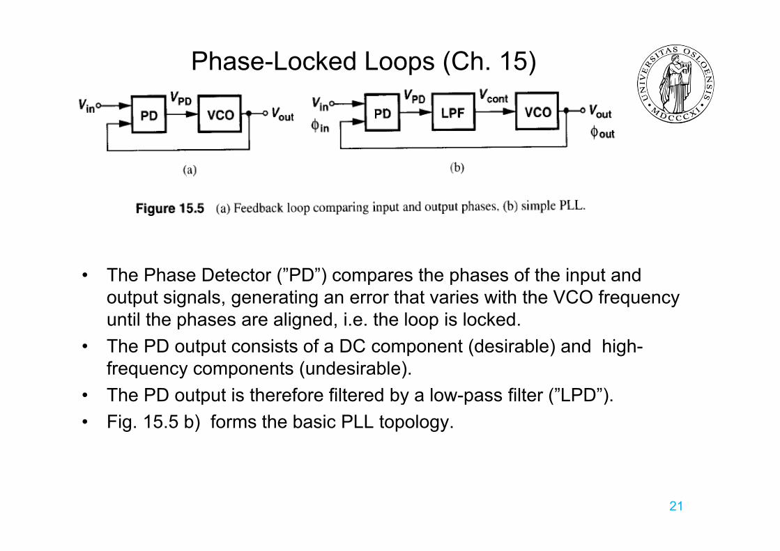
Phase-Locked Loops (Ch. 15)
• The Phase Detector (”PD”) compares the phases of the input and• The Phase Detector ( PD ) compares the phases of the input and output signals, generating an error that varies with the VCO frequencyuntil the phases are aligned, i.e. the loop is locked.
• The PD output consists of a DC component (desirable) and high-frequency components (undesirable).
• The PD output is therefore filtered by a low-pass filter (”LPD”).The PD output is therefore filtered by a low pass filter ( LPD ).• Fig. 15.5 b) forms the basic PLL topology.
21
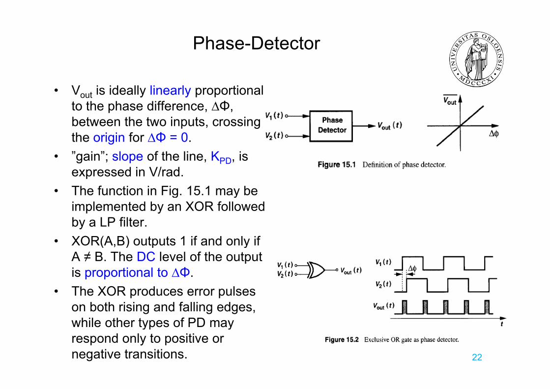
Phase-Detector
• Vout is ideally linearly proportionalto the phase difference ∆Φto the phase difference, ∆Φ, between the two inputs, crossingthe origin for ∆Φ = 0.
• ”gain”; slope of the line, KPD, is expressed in V/rad.
• The function in Fig. 15.1 may beThe function in Fig. 15.1 may be implemented by an XOR followedby a LP filter.XOR(A B) outputs 1 if and only if• XOR(A,B) outputs 1 if and only ifA ≠ B. The DC level of the output is proportional to ∆Φ.
• The XOR produces error pulses on both rising and falling edges, while other types of PD maye ot e types o ayrespond only to positive or negative transitions. 22
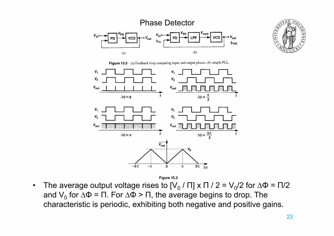
Phase Detector
• The average output voltage rises to [V0 / Π] x Π / 2 = V0/2 for ∆Φ = Π/2 and V0 for ∆Φ = Π. For ∆Φ > Π, the average begins to drop. The 0 , g g pcharacteristic is periodic, exhibiting both negative and positive gains.
23
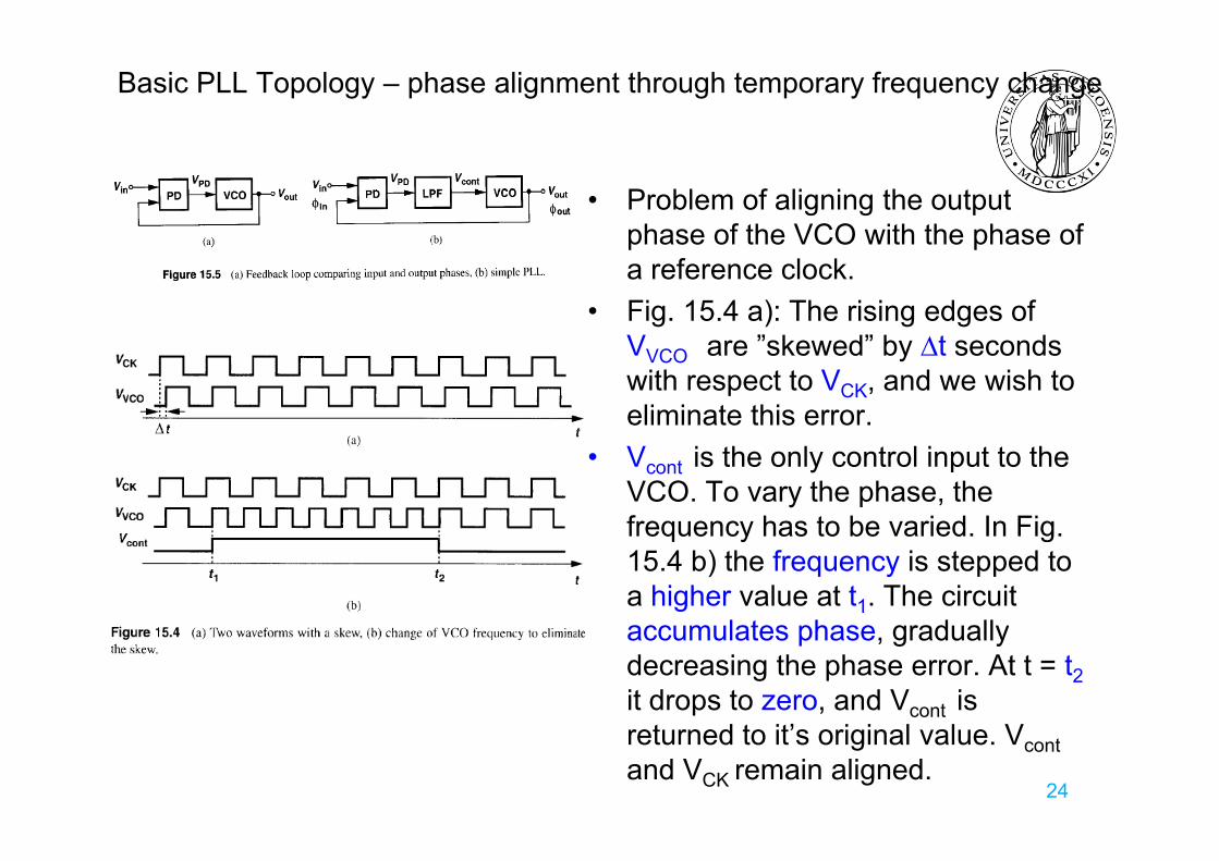
Basic PLL Topology – phase alignment through temporary frequency change
• Problem of aligning the output phase of the VCO with the phase ofphase of the VCO with the phase ofa reference clock.
• Fig. 15.4 a): The rising edges ofVVCO are ”skewed” by ∆t secondswith respect to VCK, and we wish to eliminate this error.
• Vcont is the only control input to theVCO. To vary the phase, thefrequency has to be varied In Figfrequency has to be varied. In Fig. 15.4 b) the frequency is stepped to a higher value at t1. The circuitaccumulates phase graduallyaccumulates phase, graduallydecreasing the phase error. At t = t2it drops to zero, and Vcont is
’returned to it’s original value. Vcontand VCK remain aligned.
24
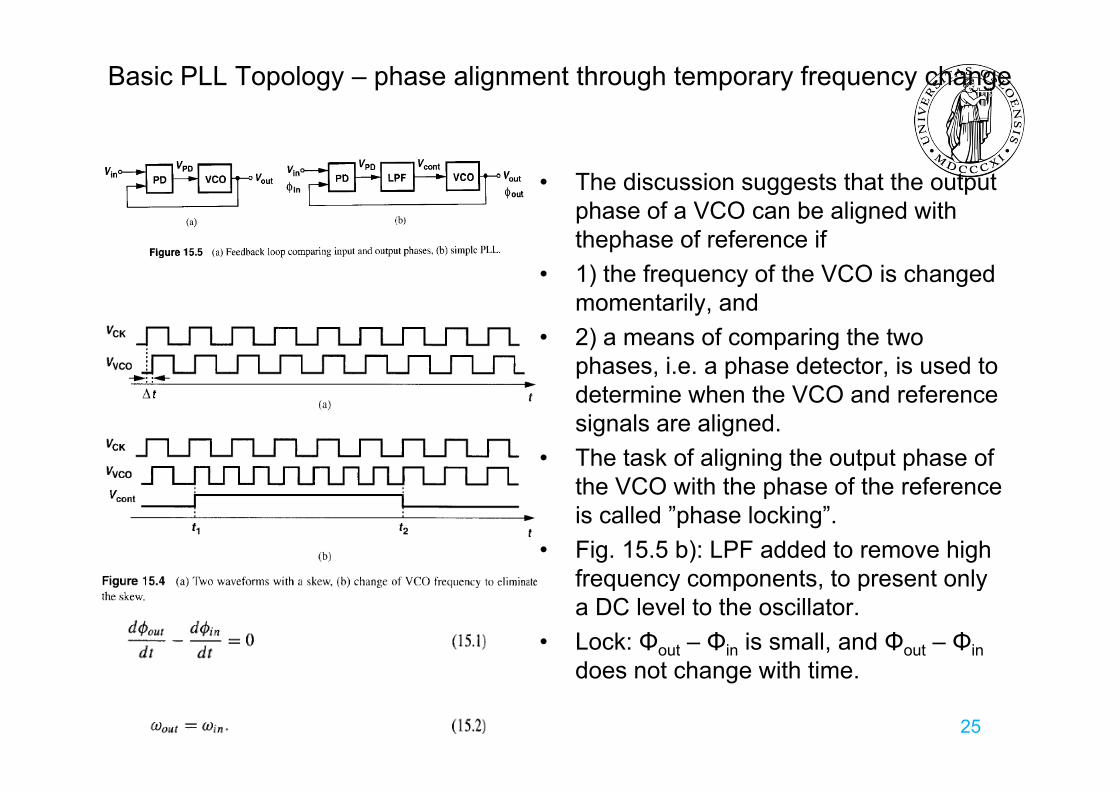
Basic PLL Topology – phase alignment through temporary frequency change
• The discussion suggests that the output phase of a VCO can be aligned withphase of a VCO can be aligned withthephase of reference if
• 1) the frequency of the VCO is changedmomentarily andmomentarily, and
• 2) a means of comparing the twophases, i.e. a phase detector, is used to determine when the VCO and referencedetermine when the VCO and referencesignals are aligned.
• The task of aligning the output phase ofthe VCO with the phase of the referencethe VCO with the phase of the referenceis called ”phase locking”.
• Fig. 15.5 b): LPF added to remove highfrequency components to present onlyfrequency components, to present onlya DC level to the oscillator.
• Lock: Φout – Φin is small, and Φout – Φind t h ith tidoes not change with time.
25
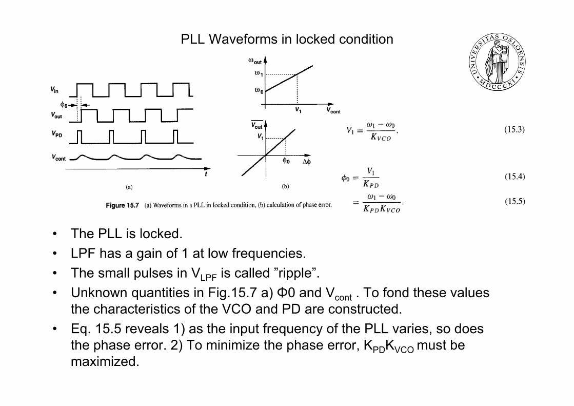
PLL Waveforms in locked condition
• The PLL is locked.LPF h i f 1 t l f i• LPF has a gain of 1 at low frequencies.
• The small pulses in VLPF is called ”ripple”.• Unknown quantities in Fig 15 7 a) Φ0 and V t To fond these valuesUnknown quantities in Fig.15.7 a) Φ0 and Vcont . To fond these values
the characteristics of the VCO and PD are constructed.• Eq. 15.5 reveals 1) as the input frequency of the PLL varies, so does
th h 2) T i i i th h K K t bthe phase error. 2) To minimize the phase error, KPDKVCO must be maximized.
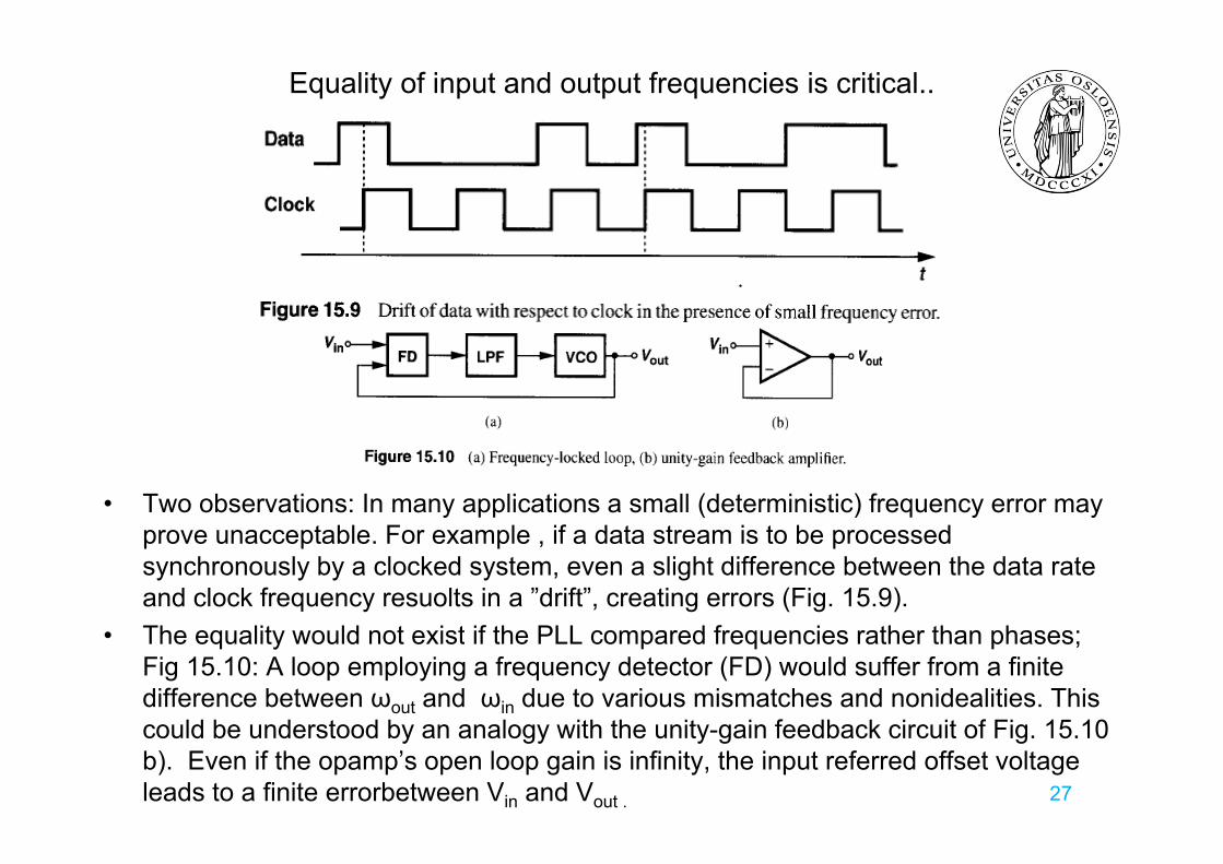
Equality of input and output frequencies is critical..
• Two observations: In many applications a small (deterministic) frequency error mayprove unacceptable For example if a data stream is to be processedprove unacceptable. For example , if a data stream is to be processedsynchronously by a clocked system, even a slight difference between the data rate and clock frequency resuolts in a ”drift”, creating errors (Fig. 15.9).Th lit ld t i t if th PLL d f i th th h• The equality would not exist if the PLL compared frequencies rather than phases; Fig 15.10: A loop employing a frequency detector (FD) would suffer from a finitedifference between ωout and ωin due to various mismatches and nonidealities. This could be understood by an analogy with the unity gain feedback circuit of Fig 15 10could be understood by an analogy with the unity-gain feedback circuit of Fig. 15.10 b). Even if the opamp’s open loop gain is infinity, the input referred offset voltageleads to a finite errorbetween Vin and Vout . 27
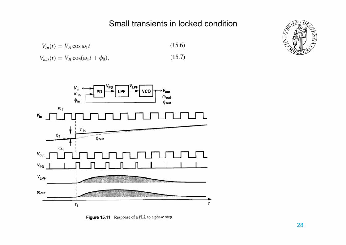
Small transients in locked condition
28
IC China 29

Preliminary plan for next week..y p
• http://www.uio.no/studier/emner/matnat/ifi/INF4420/v11/undervisningsplan.xmlM PLL ( h t 15 i ”R i”)• More on PLLs (chapter 15 in ”Razavi”)
• Report writing and layout (ch. 18)
30


![IEEE TRANSACTIONS ON SIGNAL PROCESSING, VOL. 65 ......[1]–[7]. In practice, free-running oscillators and phase-locked loops are widely used, for which phase noise is described by](https://static.fdocuments.in/doc/165x107/60fe62d9c8df1a058213904b/ieee-transactions-on-signal-processing-vol-65-1a7-in-practice.jpg)