Orr Michael Golan Alexander Svetlitza Karen...
23
Preformed By: Orr Michael Golan Karen Goldberg 1 Supervised By: Alexander Svetlitza
Transcript of Orr Michael Golan Alexander Svetlitza Karen...

Preformed By:
Orr Michael Golan
Karen Goldberg
1
Supervised By:
Alexander Svetlitza

Presentation Outline Project Objective
Theoretical Background
DC to DC Buck Converter
HFSS
Inductor Requirements
Modeled and Simulated Devices
Bondwires inductor with magnetic core
Magnetic materials
Skin depth effect
Conclusions
2

Project Objective Study and implement high performance bond wire MEMS
Inductors with magnetic cores, assess their performance
using the HFSS simulator, and measure the produced
inductors with Agilent impedance analyzer
3

Theoretical Background
A buck converter is a step-down DC to
DC converter.
Theory of operation:
• Closed state – The inductor stores
energy
• Open state - The inductor discharges the
stored energy
The output voltage is relative to the duty
cycle:
4
0
o i
D T T
V D V

Theoretical Background
HFSS is a high performance industry-standard
electromagnetic field simulator employing the
finite-element method and adaptive meshing for
arbitrary 3D volumetric passive device modeling.
It integrates simulation, visualization, solid
modeling and automation in an easy to learn
environment where solutions to 3D EM models are
quickly and accurately obtained.
5

Inductor Requirements Resistance:
Inductance:
Current:
Frequency Range:
6
0.3R
0.5L H
1I A
1 10 MHz

Modeled and Simulated Devices
7
2L nH
4L nH
Getting Started & Sanity check – 1-
turn planar square spiral inductor
simulation
L Obtained:
L Expected:
Cause: Low number of turns

Modeled and Simulated Devices
1 turn planar square Inductor with magnetic
material FeCoNi:
UnSimulatable!!
8

Modeled and Simulated Devices Straight inductor surrounded by slotted
magnetic materials FeCoNi & CoZrTa
Expected inductance according to article:
Inductance obtained in HFSS simulation:
9
3.8L nH
3.966L nH

Modeled and Simulated Devices Spiral inductor surrounded with magnetic
material CoZrTa
Expected inductance according to article:
Inductance obtained in HFSS simulation:
10
160L nH
198 200L nH
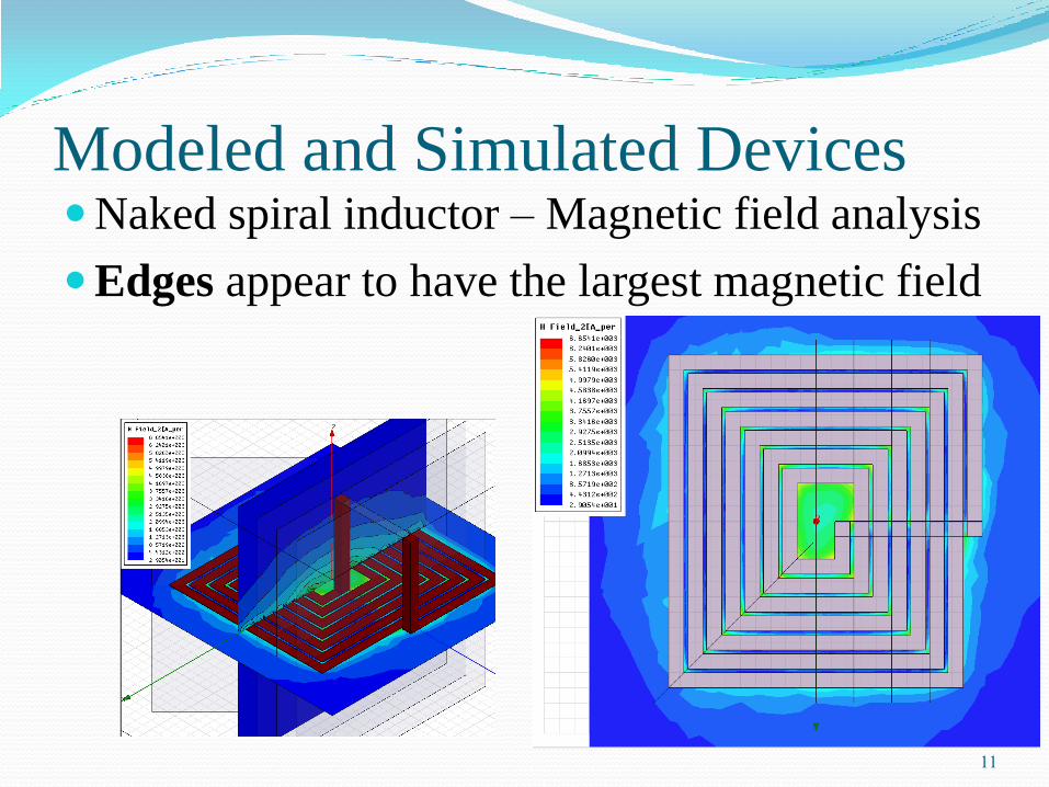
Modeled and Simulated Devices Naked spiral inductor – Magnetic field analysis
Edges appear to have the largest magnetic field
11

Modeled and Simulated Devices Meander matrix inductor – a direct application
of the naked spiral inductor results.
High Resistance, causing low Quality factor, and
too low Inductance
12

Modeled and Simulated Devices Counter-symmetry across inner circle
bond wires array, with magnetic material
Central loop containing high current over
small area, increases magnetic flux in the
middle
Geometry causing extremely
uniform field in the middle
of the array
13

Modeled and Simulated Devices Bond wires (BW) as an inductors with magnetic
cores
Properties:
2 mm outer diameter
1 mm inner diameter
0.3 um height
Magnetic core material
25-50[um] BW diameter
(Skin depth effect)
Either single or double BW loop
14

Magnetic Core Material Desired Properties:
High permeability for all frequencies in range
Low conductivity
Low magnetic losses
Compatible size
Two materials found compatible are ferrite #43
and ferrite #61 by “Fair-Rite”
15

Properties of Fair-Rite #43 ferrite
16

Properties of Fair-Rite #61 ferrite
17

Permeability modeled as complex number:
Real part responsible for B/H ratio
Imaginary part corresponds to power losses (Magnetic Losses)
Both are independent functions of frequency
Exact loss is geometry dependent. Generalization from
Maxwell's Equations:
This effect can be seen as a rise in resistivity as the
frequency grows.
Complex Permeability Effects
18

In AC regimes, current only partially permeate the
conductor through which it flows. It runs along the outer
shell and penetrates up to a skin depth of:
This effect could cause the effective area of conductance
(for resistance calculations) to be smaller than the
physical area - which would cause unnecessary losses in
the material.
2 7
1 1
4 10m
S f MHzm
Skin Depth Effect
19

The skin depth of gold, aluminum, and copper is:
We are interested in
gold and copper
Minimal skin depth
for both metals is 20-25 [um]
copper conductors are 100[um]x5[um] fully
permeated for all F no losses due to skin effect
In order to avoid these losses for all frequency
range, BW must have a diameter of up to 50[um]
Skin Depth Effect
20

D=25-50 [um] BWs using ferrite #43 Increasing BW diameter BW reduces series
resistance for all F only for
By expanding the diameter, the inductance decreases
by only 0.3%, whereas the resistance decreases by
62.5%!!!
21
50D m

Single or Parallel BWs?
22
Parallel resistors cause lower resistance than single
resistor
The higher the cross-sectional area is, the lower the
Resistance:
2
50 50 2
22
25 25
25 2
252
25
1 where D is the BW Diameter
2
For D=50 :
1
25
For 2 Parallel BW each with D=25 :
1
252 1
212 252
252
2
OneBW m D m
D m D m
Two Parallel BWs m
D m
Two Parallel BWs m O
RD
m
R R
m
R RR
R
R R
50ne BW m

Conclusions…
23
Toroidal inductor models are superior to planar models
for our set of requirements
With current magnetic material we cannot generate
enough inductance by using small inductors
Once a suitable magnetic material is found, optimization
is possible (and easy)