
Organic Solar Cells with Near-unity Charge Generation Yield
14
1 Supporting Information Organic Solar Cells with Near-unity Charge Generation Yield Wei Li*, Stefan Zeiske, Oskar J. Sandberg*, Drew B. Riley, Paul Meredith & Ardalan Armin* Sustainable Advanced Materials (Sê r SAM), Department of Physics, Swansea University Singleton Park, Swansea SA2 8PP, UK Email: [email protected]; [email protected]; [email protected]; Device fabrication: Chemical definitions: Poly(3,4-ethylenedioxythiophene) polystyrene sulfonate (PEDOT:PSS); poly[(2,6-(4,8-bis(5-(2-ethylhexyl-3-fluoro)thiophen-2-yl)-benzo[1,2-b:4,5-b’]dithiophene))-alt- (5,5-(1’,3’-di-2-thienyl-5’,7’-bis(2-ethylhexyl)benzo[1’,2’-c:4’,5’-c’]dithiophene-4,8-dione)] (PM6); 2,2'-((2Z,2'Z)-((12,13-bis(2-ethylhexyl)-3,9-diundecyl-12,13-dihydro- [1,2,5]thiadiazolo[3,4-e]thieno[2",3’':4’,5']thieno[2',3':4,5]pyrrolo[3,2-g]thieno[2',3':4,5]thieno[3,2- b]indole-2,10-diyl)bis(methanylylidene))bis(5,6-difluoro-3-oxo-2,3-dihydro-1H-indene-2,1- diylidene))dimalononitrile (Y6); 2,2'- [[12,13-Bis(2-butyloctyl)-12,13-dihydro-3,9- dinonylbisthieno[2'',3'':4',5']thieno[2',3':4,5]pyrrolo[3,2-e:2',3'-g][2,1,3]benzothiadiazole-2,10- diyl]bis[methylidyne(5,6-chloro-3-oxo-1H-indene-2,1(3H)-diylidene) ]]bis[propanedinitrile](BTP- eC9); 3,9-bis(2-methylene-(3-(1,1-dicyanomethylene)-indanone))-5,5,11,11-tetrakis(4- hexylphenyl)-dithieno[2,3-d:2’,3’-d’]-s-indaceno[1,2-b:5,6-b’]dithiophene (ITIC); (5Z)-3-ethyl-2- sulfanylidene-5-[[4-[9,9,18,18-tetrakis(2-ethylhexyl)-15-[7-[(Z)-(3-ethyl-4-oxo-2-sulfanylidene- 1,3-thiazolidin-5-ylidene)methyl]-2,1,3-benzothiadiazol-4-yl]-5,14- dithiapentacyclo[10.6.0.03,10.04,8.013,17]octadeca-1(12),2,4(8),6,10,13(17),15-heptaen-6-yl]- 2,1,3-benzothiadiazol-7-yl]methylidene]-1,3-thiazolidin-4-one (EH-IDTBR); 2,9-Bis[3- (dimethyloxidoamino)propyl]anthra[2,1,9-def:6,5,10-d'e'f']diisoquinoline-1,3,8,10(2H,9H)-tetrone (PDINO). Materials: PEDOT: PSS was purchased from Heraeus. PM6, Y6, BTP-eC9, EH-IDTBR, and PDINO were purchased from Solarmer. PBDB-T, and ITIC were purchased from Nanjing Zhiyan. ITO was purchased from the Kintec Company. Electronic Supplementary Material (ESI) for Energy & Environmental Science. This journal is © The Royal Society of Chemistry 2021
Transcript of Organic Solar Cells with Near-unity Charge Generation Yield
1
Supporting Information
Organic Solar Cells with Near-unity Charge Generation Yield
Wei Li*, Stefan Zeiske, Oskar J. Sandberg*, Drew B. Riley, Paul Meredith & Ardalan Armin*
Sustainable Advanced Materials (Sêr SAM), Department of Physics, Swansea University
Singleton Park, Swansea SA2 8PP, UK
Email: [email protected]; [email protected]; [email protected];
Device fabrication:
Chemical definitions: Poly(3,4-ethylenedioxythiophene) polystyrene sulfonate (PEDOT:PSS);
poly[(2,6-(4,8-bis(5-(2-ethylhexyl-3-fluoro)thiophen-2-yl)-benzo[1,2-b:4,5-b’]dithiophene))-alt-
(5,5-(1’,3’-di-2-thienyl-5’,7’-bis(2-ethylhexyl)benzo[1’,2’-c:4’,5’-c’]dithiophene-4,8-dione)]
(PM6); 2,2'-((2Z,2'Z)-((12,13-bis(2-ethylhexyl)-3,9-diundecyl-12,13-dihydro-
[1,2,5]thiadiazolo[3,4-e]thieno[2",3’':4’,5']thieno[2',3':4,5]pyrrolo[3,2-g]thieno[2',3':4,5]thieno[3,2-
b]indole-2,10-diyl)bis(methanylylidene))bis(5,6-difluoro-3-oxo-2,3-dihydro-1H-indene-2,1-
diylidene))dimalononitrile (Y6); 2,2'- [[12,13-Bis(2-butyloctyl)-12,13-dihydro-3,9-
dinonylbisthieno[2'',3'':4',5']thieno[2',3':4,5]pyrrolo[3,2-e:2',3'-g][2,1,3]benzothiadiazole-2,10-
diyl]bis[methylidyne(5,6-chloro-3-oxo-1H-indene-2,1(3H)-diylidene) ]]bis[propanedinitrile](BTP-
eC9); 3,9-bis(2-methylene-(3-(1,1-dicyanomethylene)-indanone))-5,5,11,11-tetrakis(4-
hexylphenyl)-dithieno[2,3-d:2’,3’-d’]-s-indaceno[1,2-b:5,6-b’]dithiophene (ITIC); (5Z)-3-ethyl-2-
sulfanylidene-5-[[4-[9,9,18,18-tetrakis(2-ethylhexyl)-15-[7-[(Z)-(3-ethyl-4-oxo-2-sulfanylidene-
1,3-thiazolidin-5-ylidene)methyl]-2,1,3-benzothiadiazol-4-yl]-5,14-
dithiapentacyclo[10.6.0.03,10.04,8.013,17]octadeca-1(12),2,4(8),6,10,13(17),15-heptaen-6-yl]-
2,1,3-benzothiadiazol-7-yl]methylidene]-1,3-thiazolidin-4-one (EH-IDTBR); 2,9-Bis[3-
(dimethyloxidoamino)propyl]anthra[2,1,9-def:6,5,10-d'e'f']diisoquinoline-1,3,8,10(2H,9H)-tetrone
(PDINO).
Materials: PEDOT: PSS was purchased from Heraeus. PM6, Y6, BTP-eC9, EH-IDTBR, and PDINO
were purchased from Solarmer. PBDB-T, and ITIC were purchased from Nanjing Zhiyan. ITO was
purchased from the Kintec Company.
Electronic Supplementary Material (ESI) for Energy & Environmental Science.This journal is © The Royal Society of Chemistry 2021
2
Substrate preparation: Commercial patterned ITO coated glass substrates were cleaned in
deionized (DI) water, acetone and 2-propanol by sequential sonication for 10 minutes. The cleaned
substrates were first dried by nitrogen and then baked on hotplate at 110 oC for 10 minutes. Afterwards,
the substrates were treated in a UV-Ozone cleaner (Ossila, L2002A2-UK) for 20 minutes before the
deposition of hole transport and electron transport layers.
PBDB-T:EH-IDTBR: PBDB-T: EH-IDTBR devices were fabricated with an inverted structure
(ITO/ZnO/PBDB-T: EH-IDTBR /MoO3/Ag). A ZnO solution was prepared by dissolving 200 mg of
zinc acetate dihydrate in 2-methoxyethanol (2ml) and ethanolamine (56µl). The solution was stirred
overnight under ambient conditions and spin-coated onto ITO substrates (4000 rpm resulting in a
thickness of approximately 30 nm) followed by thermal annealing at 200 °C for 60 minutes. PBDB-
T: EH-IDTBR was dissolved in a (99.5:0.5) CB:DIO solution with a donor: acceptor ratio of 1:1 by
weight. The thicknesses of PBBD-T:EH-IDTBR films were adjusted by changing the concentration
of the solution and spin-coating speed (40 mg ml-1 CB:DIO solution with 700 rpm for 310 nm films,
35 mg ml-1 CB:DIO solution with 700 rpm for 270 nm films, 30 mg ml-1 CB:DIO solution with 700
rpm for 200 nm films, 24 mg ml-1 CB:DIO solution with 700 rpm for 170 nm films, 14 mg ml-1
CB:DIO solution with 700 rpm for 90 nm films, 10 mg ml-1 CB:DIO solution with 700 rpm for 50
nm films). The active layers were further treated with thermal annealing at 100 oC for 10 minutes.
Afterwards, 7 nm of MoO3 and 100 nm of Ag were evaporated as the top electrode.
PM6:ITIC: PM6:ITIC devices were fabricated with a conventional device structure
(ITO/PEDOT:PSS/PM6:ITIC/PDINO/Ag). PEDOT: PSS solution was first diluted with the same
volume of water and then cast at 4000 rpm on ITO substrates followed by thermal annealing at 155
oC for 15 min to form a 10 nm film. PM6: ITIC was dissolved in a (99.5:0.5) CF:DIO solution with
a donor: acceptor ratio of 1:1 by weight. The thicknesses of PM6:ITIC films were adjusted by
changing the concentration of the solution and spin-coating speed (36 mg ml-1 CF:DIO solution with
2000 rpm for 470 nm films, 32 mg ml-1 CF:DIO solution with 2000 rpm for 288 nm films, 25 mg ml-
1 CF:DIO solution with 2000 rpm for 180 nm films, 20 mg ml-1 CF:DIO solution with 3000 rpm for
130 nm films, 14 mg ml-1 CF:DIO solution with 3000 rpm for 90 nm films, 12 mg ml-1 CF:DIO
solution with 3000 rpm for 60 nm films). The active layers were further thermally annealed at 100 oC
for 10 minutes. Afterwards, 1 mg ml-1 PDINO solution was spin-coated on PM6: ITIC film at 2000
rpm to form 10 nm films, and 100 nm of Ag was evaporated as the top electrode.
3
PM6:Y6: PM6:Y6 devices were fabricated with a conventional structure (ITO/PEDOT:
PSS/PM6:Y6/PDINO/Ag). PEDOT: PSS solution was first diluted with the same volume of water
and then cast at 4000 rpm on ITO substrates followed by thermal annealing at 155 oC for 15 min to
form a 10 nm film. PM6:Y6 was dissolved in a CF:CN (99.5:0.5) solution with a donor: acceptor
ratio of 1:1.2 by weight. The thicknesses of PM6:Y6 films were adjusted by changing the
concentration of the solution and the spin‐coating speed (40 mg ml-1 CF:CN solution with 4000 rpm
for 390 nm, 35 mg ml-1 CF:DIO solution with 4000 rpm for 310 nm, 30 mg ml-1 CF:DIO solution
with 4000 rpm for 260 nm, 25 mg ml-1 CF:DIO solution with 4000 rpm for 190 nm, 20 mg ml-1
CF:DIO solution with 4000 rpm for 160 nm, 16 mg ml-1 CF:DIO solution with 2000 rpm for 109 nm,
5 mg ml-1 CF:DIO solution with 2000 rpm for 30 nm). The active layers were further thermally
annealed at 100 oC for 10 minutes. Afterwards, 1 mg ml-1 PDINO solution was spin-coated on PM6:
Y6 films at 2000 rpm to form 10 nm films, and 100 nm of Ag was evaporated as the top electrode.
PM6:BTP-eC9: PM6:BTP-eC9 devices were fabricated with a conventional structure
(ITO/PEDOT:PSS/PM6:BTP-eC9/PDINO/Ag). PEDOT: PSS solution was first diluted with the
same volume of water and then cast at 4000 rpm on ITO substrate and followed by thermal annealing
at 155 oC for 15 min to form a 10 nm film. PM6:BTP-eC9 was dissolved in a CF:DIO (99.5:0.5)
solution with a donor: acceptor ratio of 1:1.2 by weight. The thicknesses of PM6:BTP-eC9 films were
adjusted by changing the concentration of the solution and the spin‐coating speed (40 mg ml-1 CF:DIO
solution with 2000 rpm for 446 nm, 35 mg ml-1 CF:DIO solution with 2000 rpm for 340 nm, 30 mg
ml-1 CF:DIO solution with 2000 rpm for 293 nm, 25 mg ml-1 CF:DIO solution with 2000 rpm for 260
nm, 23 mg ml-1 CF:DIO solution with 3000 rpm for 200 nm, 20 mg ml-1 CF:DIO solution with 2000
rpm for 160 nm, 16 mg ml-1 CF:DIO solution with 3000 rpm for 90 nm, 12 mg ml-1 CF:DIO solution
with 3000 rpm for 60 nm). Afterwards, 1 mg ml-1 PDINO solution was spin-coated on PM6: BTP-
eC9 film at 2000 rpm to form 10 nm films, and 100 nm of Ag was evaporated as the top electrode.
The thicknesses of all the above films are measured by ellipsometry.
4
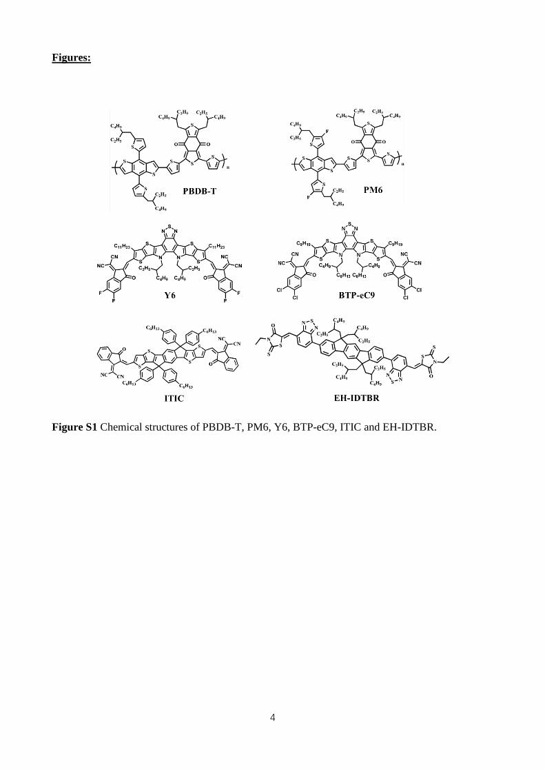
Figures:
Figure S1 Chemical structures of PBDB-T, PM6, Y6, BTP-eC9, ITIC and EH-IDTBR.
5
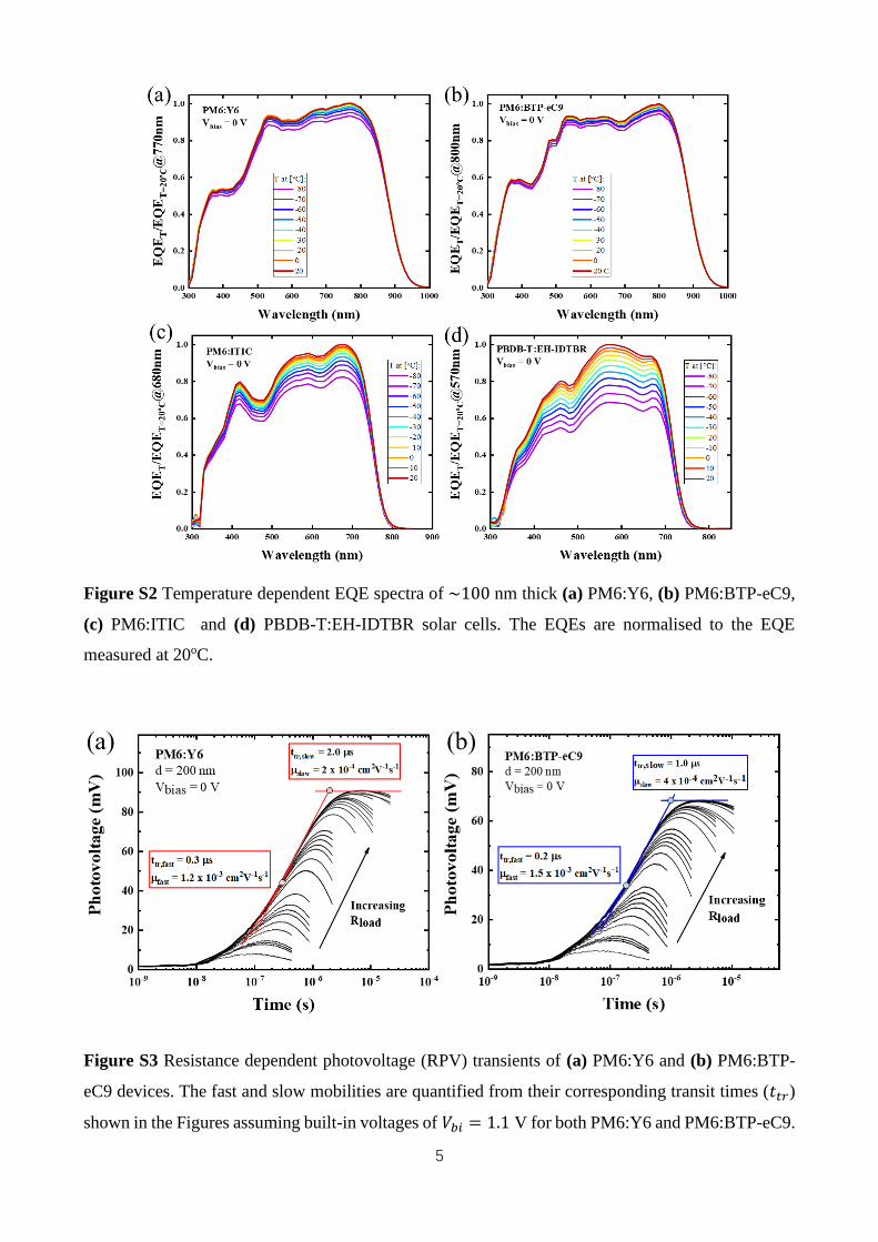
Figure S2 Temperature dependent EQE spectra of ~100 nm thick (a) PM6:Y6, (b) PM6:BTP-eC9,
(c) PM6:ITIC and (d) PBDB-T:EH-IDTBR solar cells. The EQEs are normalised to the EQE
measured at 20oC.
Figure S3 Resistance dependent photovoltage (RPV) transients of (a) PM6:Y6 and (b) PM6:BTP-
eC9 devices. The fast and slow mobilities are quantified from their corresponding transit times (𝑡𝑡𝑟)
shown in the Figures assuming built-in voltages of 𝑉𝑏𝑖 = 1.1 V for both PM6:Y6 and PM6:BTP-eC9.
6
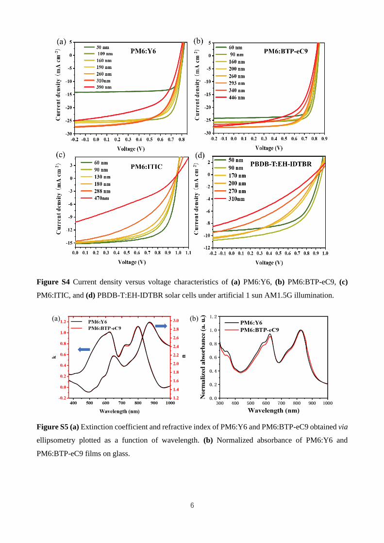
Figure S4 Current density versus voltage characteristics of (a) PM6:Y6, (b) PM6:BTP-eC9, (c)
PM6:ITIC, and (d) PBDB-T:EH-IDTBR solar cells under artificial 1 sun AM1.5G illumination.
Figure S5 (a) Extinction coefficient and refractive index of PM6:Y6 and PM6:BTP-eC9 obtained via
ellipsometry plotted as a function of wavelength. (b) Normalized absorbance of PM6:Y6 and
PM6:BTP-eC9 films on glass.
7
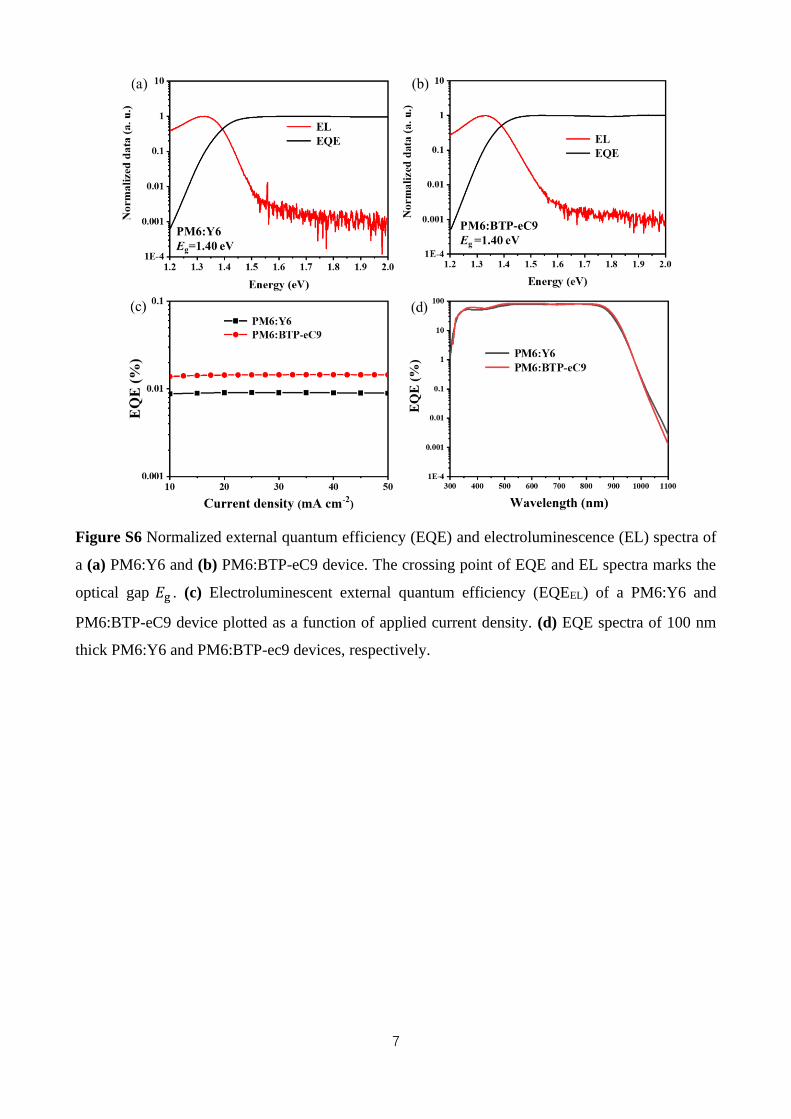
Figure S6 Normalized external quantum efficiency (EQE) and electroluminescence (EL) spectra of
a (a) PM6:Y6 and (b) PM6:BTP-eC9 device. The crossing point of EQE and EL spectra marks the
optical gap 𝐸g . (c) Electroluminescent external quantum efficiency (EQEEL) of a PM6:Y6 and
PM6:BTP-eC9 device plotted as a function of applied current density. (d) EQE spectra of 100 nm
thick PM6:Y6 and PM6:BTP-ec9 devices, respectively.
8
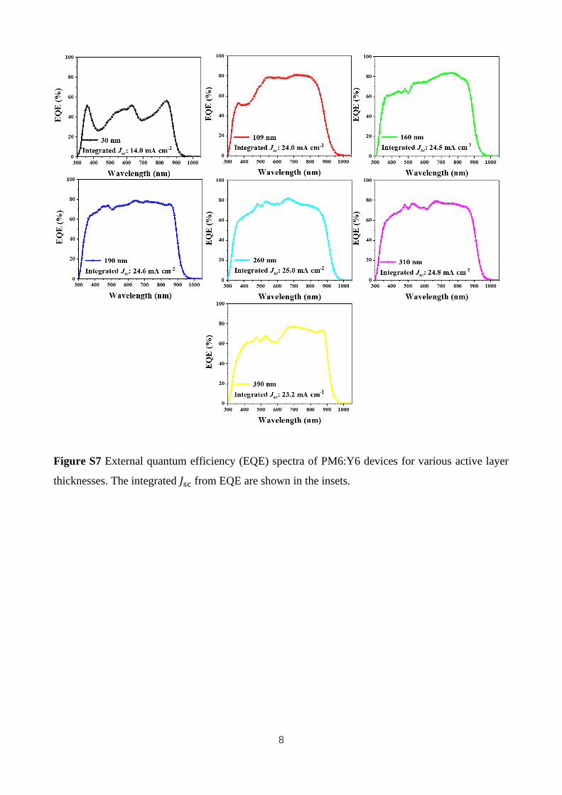
Figure S7 External quantum efficiency (EQE) spectra of PM6:Y6 devices for various active layer
thicknesses. The integrated 𝐽sc from EQE are shown in the insets.
9
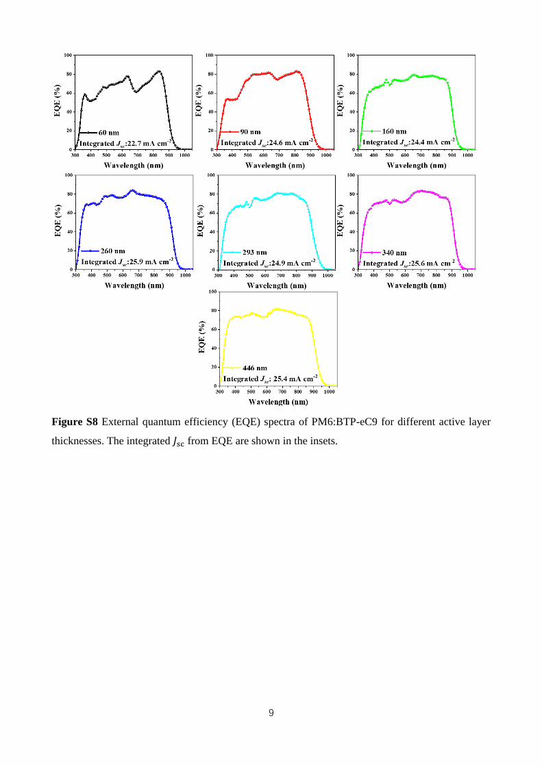
Figure S8 External quantum efficiency (EQE) spectra of PM6:BTP-eC9 for different active layer
thicknesses. The integrated 𝐽sc from EQE are shown in the insets.
10
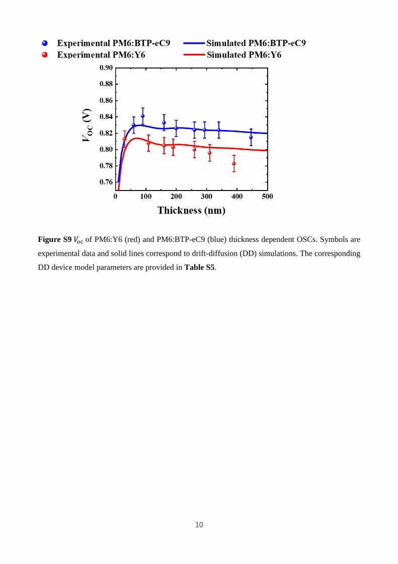
Figure S9 𝑉oc of PM6:Y6 (red) and PM6:BTP-eC9 (blue) thickness dependent OSCs. Symbols are
experimental data and solid lines correspond to drift-diffusion (DD) simulations. The corresponding
DD device model parameters are provided in Table S5.
11
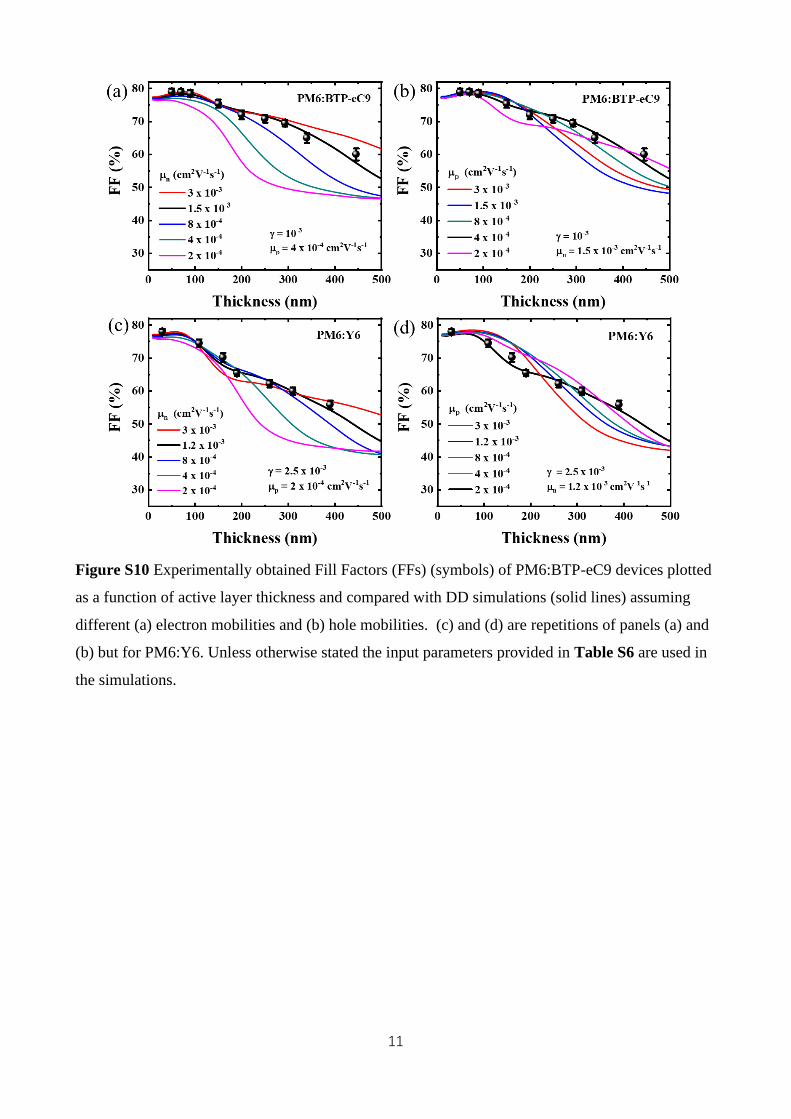
Figure S10 Experimentally obtained Fill Factors (FFs) (symbols) of PM6:BTP-eC9 devices plotted
as a function of active layer thickness and compared with DD simulations (solid lines) assuming
different (a) electron mobilities and (b) hole mobilities. (c) and (d) are repetitions of panels (a) and
(b) but for PM6:Y6. Unless otherwise stated the input parameters provided in Table S6 are used in
the simulations.
12
Tables:
Table S1 Photovoltaic parameters of PM6:Y6 devices with different active layer thicknesses.
Thickness (nm) FF
[%]
Jsc
[mA cm-2]
Voc
[V]
PCEmax (PCEavg)
[%]
30 nm 78.9 14.1 0.81 9.1 (8.7±0.4)
109 nm 76.6 25.1 0.81 15.6 (15.2±0.4)
160 nm 70.4 25.2 0.81 14.3(13.9±0.4)
190 nm 65.3 25.4 0.80 13.4 (13.2±0.2)
260 nm 61.9 26.7 0.80 13.2 (12.8±0.4)
310 nm 61.4 26.8 0.80 13.1 (12.6±0.5)
390 nm 55.7 23.9 0.78 10.5 (9.3±1.2)
Table S2 Photovoltaic parameters of PM6:BTP-eC9 devices with different active layer thicknesses.
Thickness (nm) FF
[%]
Jsc
[mA cm-2]
Voc
[V]
PCEmax (PCEavg)
[%]
60 nm 78.5 24.1 0.83 15.7 (15.3±0.4)
90 nm 79.1 25.7 0.84 17.1 (16.7±0.2)
160 nm 76.9 25.6 0.83 16.4 (16.2±0.2)
200 nm 72.3 27.7 0.83 16.5 (16.1±0.3)
260 nm 71.8 27.8 0.82 16.4 (15.9±0.3)
293 nm 71.3 27.7 0.82 16.2 (15.7±0.4)
340 nm 66.1 27.2 0.82 14.8 (14.3±0.5)
446 nm 59.9 26.8 0.82 13.1 (12.4±0.7)
13
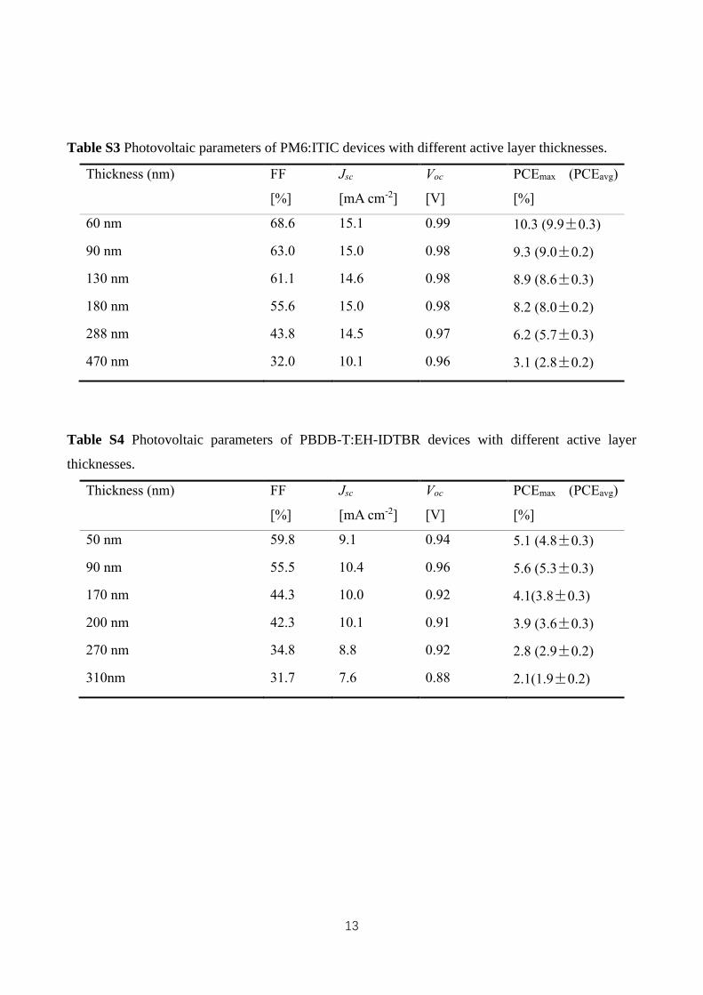
Table S3 Photovoltaic parameters of PM6:ITIC devices with different active layer thicknesses.
Thickness (nm) FF
[%]
Jsc
[mA cm-2]
Voc
[V]
PCEmax (PCEavg)
[%]
60 nm 68.6 15.1 0.99 10.3 (9.9±0.3)
90 nm 63.0 15.0 0.98 9.3 (9.0±0.2)
130 nm 61.1 14.6 0.98 8.9 (8.6±0.3)
180 nm 55.6 15.0 0.98 8.2 (8.0±0.2)
288 nm 43.8 14.5 0.97 6.2 (5.7±0.3)
470 nm 32.0 10.1 0.96 3.1 (2.8±0.2)
Table S4 Photovoltaic parameters of PBDB-T:EH-IDTBR devices with different active layer
thicknesses.
Thickness (nm) FF
[%]
Jsc
[mA cm-2]
Voc
[V]
PCEmax (PCEavg)
[%]
50 nm 59.8 9.1 0.94 5.1 (4.8±0.3)
90 nm 55.5 10.4 0.96 5.6 (5.3±0.3)
170 nm 44.3 10.0 0.92 4.1(3.8±0.3)
200 nm 42.3 10.1 0.91 3.9 (3.6±0.3)
270 nm 34.8 8.8 0.92 2.8 (2.9±0.2)
310nm 31.7 7.6 0.88 2.1(1.9±0.2)
14
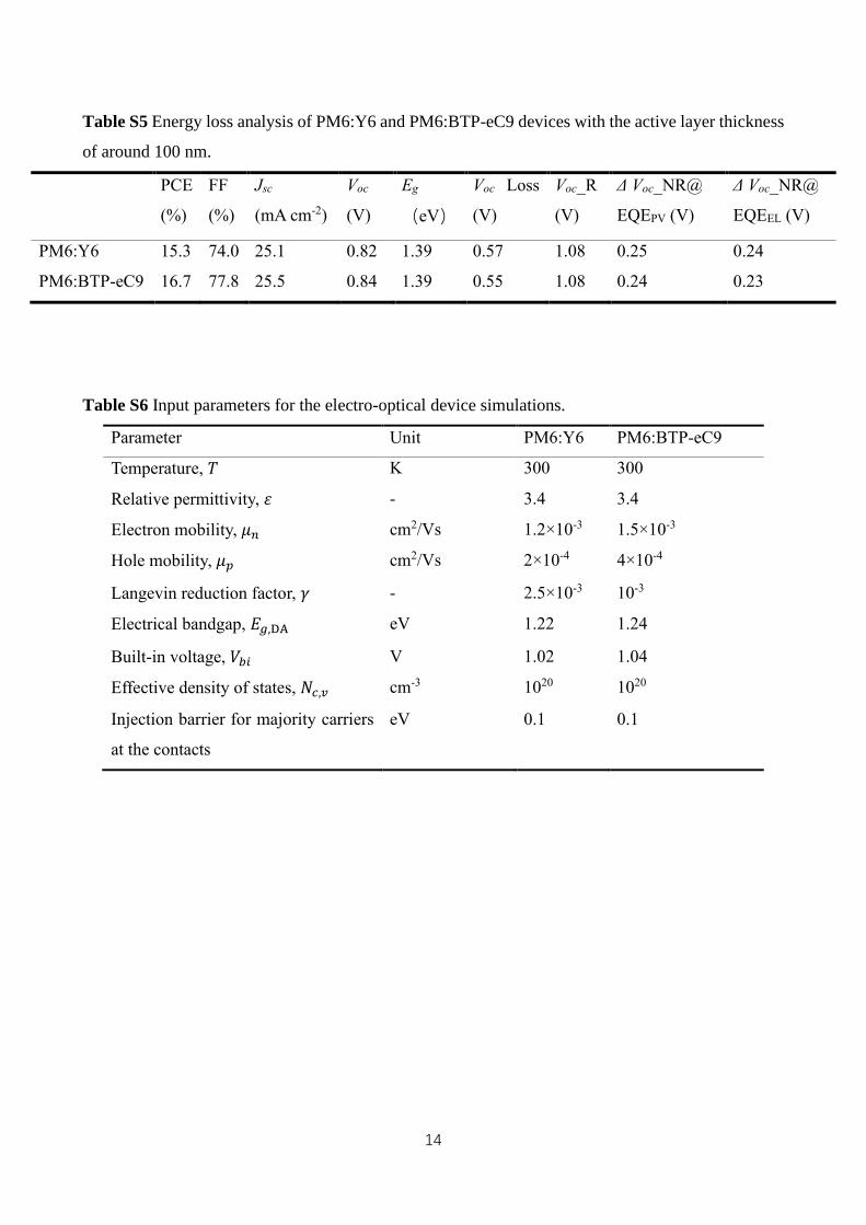
Table S5 Energy loss analysis of PM6:Y6 and PM6:BTP-eC9 devices with the active layer thickness
of around 100 nm.
PCE
(%)
FF
(%)
Jsc
(mA cm-2)
Voc
(V)
Eg
(eV)
Voc Loss
(V)
Voc_R
(V)
Δ Voc_NR@
EQEPV (V)
Δ Voc_NR@
EQEEL (V)
PM6:Y6 15.3 74.0 25.1 0.82 1.39 0.57 1.08 0.25 0.24
PM6:BTP-eC9 16.7 77.8 25.5 0.84 1.39 0.55 1.08 0.24 0.23
Table S6 Input parameters for the electro-optical device simulations.
Parameter Unit
PM6:Y6
PM6:BTP-eC9
Temperature, 𝑇 K 300 300
Relative permittivity, 𝜀 - 3.4 3.4
Electron mobility, 𝜇𝑛 cm2/Vs 1.2×10⁻³ 1.5×10⁻³
Hole mobility, 𝜇𝑝 cm2/Vs 2×10⁻⁴ 4×10⁻⁴
Langevin reduction factor, 𝛾 - 2.5×10⁻³ 10-3
Electrical bandgap, 𝐸𝑔,DA eV 1.22 1.24
Built-in voltage, 𝑉𝑏𝑖 V 1.02 1.04
Effective density of states, 𝑁𝑐,𝑣 cm-3 1020 1020
Injection barrier for majority carriers
at the contacts
eV 0.1 0.1


![[Paris Unity meetup] - Unity 3D en entreprise](https://static.fdocuments.in/doc/165x107/55a64ec51a28ab123f8b45ab/paris-unity-meetup-unity-3d-en-entreprise.jpg)