
Introduction to Optoelectronics 1st Lecture: Optoelectronics in your neighborhood
FAKULTA ELEKTROTECHNIKY A KOMUNIKAČNÍCH TECHNOLOGIÍ VYSOKÉ UČENÍ TECHNICKÉ V BRNĚ
Optoelectronics for telecommuncations and informatics
Miloslav Filka
Poslední aktualizace 24.9.2009
2 FEEC Brno University of Technology
Content SUMMARY OF: OPTOELECTRONICS FOR TELECOMMUNICATIONS AND
INFORMATICS ............................................................................................................... 14
1 INTRODUCTION – EVOLUTION OF OPTOELECTRONICS IN TELECOMMUNICATIONS AND INFORMATICS .................................................. 16
2 TRANSMISSION PROPERTIES OF OPTICAL FIBRES ......................................... 23
2.1 ATTENUATION OF OPTICAL FIBRES ................................................................................ 25 2.2 DISPERSION IN OPTICAL FIBRES ..................................................................................... 30 2.3 ZHEORY OF TRANSMISSION OVER LIGHTGUIDES ............................................................ 40 2.4 POLYMER OPTICAL FIBRES - POF .................................................................................. 49 2.5 NEW TECHNOLOGIE SOF FIBRE MANUFACTURE .............................................................. 50
3 MANUFACTURE OF OPTICAL FIBRES .................................................................. 53
4 MANUFACTURE OF OPTICAL CABLES ................................................................. 66
4.1 PROPERTIES OF SELECTED TYPE SOF OPTICAL FIBRE ...................................................... 72
5 SPLICING TECHNICE, CONNECTORS AND COUPLERS ................................... 79
5.1 ON GENERAL PROBLEMS OF SPLICING ............................................................................ 79 5.2 NON-DEMOUNTABLE SPLICES ........................................................................................ 91 5.3 DEMOUNTABLE SPLICES ................................................................................................ 95 5.4 OPTICAL COUPLERS ..................................................................................................... 101
6 SOURCE OF LIGHT .................................................................................................... 107
6.1 LIGHT-EMITTING DIODES ............................................................................................. 108 6.2 LASER DIODES ............................................................................................................. 114 6.3 OPTOELECTRONIC TRANSMISSION COMPONENTS ......................................................... 119
7 LIGHT MODULATION AND DETECTION ............................................................ 120
7.1 MODULATION METHODS ............................................................................................. 120 7.2 DETECTION OF RADIATION .......................................................................................... 123 7.3 PARAMETERS OF RADIATION DETECTORS .................................................................... 127
8 OPTOELECTRONIC TELECOMMUNICATION SYSTEMS ............................... 129
8.1 BASIC PROBLEMS OF OPTOELECTRONIC SYSTEMS ........................................................ 133 8.2 TRANSMITTER AND RECEIVER PART SOF OPTICAL SYSTEM .......................................... 135 8.3 OPTICAL LINK CODES .................................................................................................. 140 8.4 OPTICAL LINK RANGE .................................................................................................. 143 8.5 DEPLOYMENT OF OPTOELECTRONIC SYSTEMS ............................................................. 144 8.6 OPTOELECTRONIC LINK TRACK OF 8 MBIT . S-1
DIGITAL SYSTEM ................................. 145 8.7 OPTOELECTRONIC LINK TRACK OF 34 MBIT . S-1
DIGITAL SYSTEM ............................... 148 8.8 OPTOELECTRONIC LINHK TRACK OF 140 MBIT . S-1
DIGITAL SYSTEM ...................... 150 8.9 OPTOELECTRONIC LINK TRACK OF 565 MBIT . S-1
DIGITAL SYSTEM ............................. 150 8.10 OPTOELECTRONIC SYSTEMS FOR TRANSMISSION OF ANALOGUE MODULATION ............ 151 8.11 OPTOELECTRONIC SYSTEMS FOR TRANSMISSION OF TELEVISION SIGNAL ..................... 152 8.12 OPTOELECTRONIC TRANSMISSION SYSTEMS FOR SHORT DISTANCES ............................ 153 8.13 OPTOELECTRONIC SYSTEMS FOR INDUSTRIAL APPLICATIONS ...................................... 153 8.14 LOCAL OPTICAL NETWORKS ........................................................................................ 155
Optoelectronics for telecommunications and informatics 3
8.15 CURRENT TRENDS IN OPTICAL ACCESS NETWORKS ...................................................... 167 8.16 OPTOELECTRONIC MULTIPLEY SYSTEMS ...................................................................... 173 8.17 TV OPTICAL FIBRE LINKS ............................................................................................. 187 8.18 SUBMARINE OPTICAL TRANSMISSION ........................................................................... 188 8.19 INSTALLATION OF OPTICAL ROUTES ............................................................................. 189 8.20 FREE-SPACE OPTICAL COMMUNICATION ...................................................................... 197 8.21 OPTICAL FILTERS ......................................................................................................... 205 8.22 EXPERIENCE OF BUILDING CZECHOSLOVAK OPTICAL ROUTES ..................................... 214 8.23 EXPERIENCE OF BUILDING METROPOLITAN OPTICAL NETWORK IN BRNO ..................... 215 8.24 SELECTED EXAMPLES OF OPTICAL NETWORKS OF VARIOUS OPERATORS ...................... 222 8.25 FURTHER POSSIBILITIES AND METHODS IN OPTOELECTRONICS ..................................... 225 8.26 HEALTH PROTECTION DURING WORK WITH OPTICAL LINKS .......................................... 226
9 MEASURING METHODS IN OPTICAL COMMUNICATIONS .......................... 227
9.1 METHODS OF OPTICAL FIBRE EXCITATION FOR MEASURING PURPOSES ......................... 228 9.2 MEASUREMENT ON OPTICAL FIBRES ............................................................................ 233 9.3 MECHANICAL MEASUREMENT ...................................................................................... 235 9.4 TRANSMISSION MEASUREMENT ON OPTICAL FIBRES .................................................... 236 9.5 MEASUREMENT OF OPTOELECTRONIC COMPONENTS .................................................... 253 9.6 SPECIAL MEASUREMENT METHODS .............................................................................. 254 9.7 SUPERVISION (MONITORING) OF OPTICAL NETWORKS .................................................. 255
10 PLANAR OPTICAL WAVEGUIDES ........................................................................ 256
10.1 PRINCIPLE AND FICTION OF PLANAR LIGHTQUIDES ....................................................... 256 10.2 COUPLING STRUCTURES OF PLANAR LIGHTGUIDES ....................................................... 260 10.3 APPLICATION OF PLANAR LIGHTQUIDES IN INTEGRATED OPTICS .................................. 264

4 FEEC Brno University of Technology
List of Figures OBR. 1.1: BASIC OPTICAL LINK CONNECTION .................................................................... 18 OBR. 2.1: MULTIMODE STEP-INDEX FIBRE ......................................................................... 23 OBR. 2.2: MULTIMODE FIBRE WITH VARYING REFRACTIVE INDEX ..................................... 24 OBR. 2.3: SINGLE-MODE STEP-INDEX FIBRE ...................................................................... 24 OBR. 2.4: EXAMPLES OF DIFFERENT REFRACTIVE INDEX PROFILES .................................... 25 OBR. 2.5: ATTENUATION IN FIBRE LIGHTGUIDES ............................................................... 26 OBR. 2.6: TEMPERATURE DEPENDENCE OF LIGHTGUIDE ATTENUATION ............................. 27 OBR. 2.7: DEPENDENCE OF ATTENUATION OF OPTICAL CABLE LIGHTGUIDE ON Λ AFTER 8
MONTHS OF CABLE “DROWNING” ...................................................................................... 28 OBR. 2.8: ATTENUATION CHARACTERISTIC OF OPTICAL FIBRE .......................................... 29 OBR. 2.9: PATTERN OF FREQUENCY DEPENDENCE OF REFRACTIVE INDEX ON GROUP
REFRACTIVE INDEX NS FOR SIO2 ........................................................................................ 31 OBR. 2.10: PULSE BROADENING DUE TO MATERIAL DISPERSION .......................................... 32 OBR. 2.11: DEPENDENCE OF MATERIAL DISPERSION ON Λ, FOR SIO2 ................................... 33 OBR. 2.12: PULSE PROPAGATION IN LIGHTGUIDE: A) MULTIMODE STEP-INDEX FIBRE, B)
MULTIMODE GRADIENT-INDEX FIBRE, C) SINGLE-MODE STEP-INDEX FIBRE ....................... 35 OBR. 2.13: PATTERN OF CHROMATIC DISPERSION OF CONVENTIONAL FIBRE ....................... 36 OBR. 2.14: PATTERN OF CHROMATIC DISPERSION IN FIBRES WITH SHIFTED DISPERSION
CHARACTERISTIC............................................................................................................... 37 OBR. 2.15: EXAMPLE OF CHROMATIC DISPERSION COMPENSATION OF OPTICAL ROUTE ....... 37 OBR. 2.16: EXAMPLE OF PMD - POLARIZATION MODE DISPERSION ..................................... 37 OBR. 2.17: LIGHTGUIDE TRANSMISSION OF SIGNALS: A) NORMALIZED CHARACTERISTIC, B)
RESPONSE TO THE DIRAC PULSE ........................................................................................ 42 OBR. 2.18: CURVES FOR BESSEL FUNCTIONS JO AND JE AND PROPAGATION BOUNDARIES OF
CORRESPONDING MODES ................................................................................................... 46 OBR. 2.19: PROPAGATION CONSTANT Β IN DEPENDENCE ON NORMALIZED FREQUENCY ...... 47 OBR. 2.20: DEPENDENCE OF WAVEGUIDE DISPERSION ON NORMALIZED FREQUENCY V ............ 48 OBR. 2.21: DEPENDENCE OF ATTENUATION ON WAVELENGTH IN POF ................................ 49 OBR. 2.22: POF FIBRE ......................................................................................................... 50 OBR. 2.23: PRINCIPLE OF EXCITATION INTO DOPED FIBRE, USING FUSED FIBRE SPLICE ELEMENT
51 OBR. 2.24: POLARIZATION .................................................................................................. 51 OBR. 2.25: MICROSTRUCTURE OPTICAL FIBRE .................................................................... 52 OBR. 2.26: MOF WITH ULTRA-FLAT DISPERSION CHARACTERISTIC ..................................... 52 OBR. 3.1: DRAWING OPTICAL FIBRE FROM PREFORM ................................................................ 54 OBR. 3.2: PRINCIPLE OF PREFORM MANUFACTURE BY THE OVD METHOD ........................ 56 OBR. 3.3: PRINCIPLE OF PREFORM MANUFACTURE BY THE MCVD METHOD ..................... 56 OBR. 3.4: PREFORM MANUFACTURE BY THE PCVD TECHNOLOGY .................................... 57 OBR. 3.5: PREFORM MANUFACTURE BY THE VAD TECHNOLOGY ...................................... 58 OBR. 3.6: THE “ROD IN THE TUBE” METHOD OF MANUFACTURING OPTICAL FIBRE ............ 59 OBR. 3.7: THE DOUBLE CRUCIBLE METHOD ....................................................................... 60 OBR. 3.8: PRACTICAL IMPLEMENTATION OF THE METHOD OF DOUBLE CRUCIBLE .............. 60 OBR. 3.9: REFRACTIVE INDEX OF SM FIBRE ...................................................................... 61 OBR. 3.10: REFRACTIVE INDEX PROFILE .............................................................................. 63 OBR. 4.1: DESIGN OF A SIMPLE OPTICAL CABLE: 1 – CORE, 2 – CLADDING, 3 – PRIMARY
COATING, 4 – SECONDARY COATING .................................................................................. 66 OBR. 4.2: OPTICAL CABLE: 1 – OPTICAL FIBRE, 2 – OUTER PLASTIC CLADDING, 3 – PVC
JACKET 67

Optoelectronics for telecommunications and informatics 5
OBR. 4.3: SINGLE-FIBRE OPTICAL CABLE: 1 – OPTICAL FIBRE, 2 – CUSHION, 3 – KEVLAR, 4 –
PVC 67 OBR. 4.4: SINGLE-FIBRE OPTICAL CABLE: 1 – OPTICAL FIBRE, 2 – KEVLAR REINFORCEMENT,
3 – PLASTIC JACKET ........................................................................................................... 67 OBR. 4.5: SCHEMATIC ILLUSTRATION OF COMBINED SINGLE-FIBRE OPTICAL CABLE WITH CU
PAIRS ADDED ..................................................................................................................... 68 OBR. 4.6: SIX-FIBRE OPTICAL CABLE: 1 – 19 STRENGTH MEMBERS OF KEVLAR, 2 – OPTICAL
FIBRES, 3 – FILLER, 4 – JACKET .......................................................................................... 68 OBR. 4.7: TWO-FIBRE OPTICAL CABLE: 1 – STRENGTH MEMBER, 2 – OPTICAL FIBRES, 3 –
FILLER, 4 – CUSHION, 5 – PVC JACKET .............................................................................. 68 OBR. 4.8: SEVEN-FIBRE OPTICAL CABLE ............................................................................ 69 OBR. 4.9: SEVEN-MEMBER OPTICAL CABLE: 1 – OPTICAL FIBRE, 2 – KEVLAR CLADDING, 3 –
STRENGTH MEMBERS (KEVLAR), 4 – JACKET ..................................................................... 69 OBR. 4.10: OPTICAL CABLE (DIFFERENT LOCATION OF STRENGTH MEMBERS): 1 – OPTICAL
FIBRES, 2 – STRENGTH MEMBERS, 3 – JACKET .................................................................... 69 OBR. 4.11: OPTICAL CABLE WITH LOOSELY PLACED FIBRES: 1 – STRENGTH MEMBER, 2 –
CUSHION, 3 – PLASTIC TUBE, 4 – OPTICAL FIBRE, 5 - PLASTIC COATINGS, 6 – JACKET ......... 70 OBR. 4.12: SLOTTED OPTICAL CABLE: 1 – STRENGTH MEMBER, 2 – PROFILING, 3 – FIBRE, 4 –
JACKET 70 OBR. 4.13: OPTICAL CABLE WITH CELLULAR STRUCTURE: 1 – OPTICAL FIBRES, 2 – CELLS, 3 –
PLASTIC FILLER, 4 - JACKET ............................................................................................... 70 OBR. 4.14: RIBBON ARRANGEMENT OF OPTICAL CABLE: 1 – OPTICAL CABLES LED OUT TO
CONNECTOR, 2- ARMOURING, 3 – JACKET .......................................................................... 71 OBR. 4.15: ARMOURED TYPE OF OPTICAL CABLE – SUBMARINE SEVEN-FIBRE CABLE: 1 –
OPTICAL FIBRES, 2 – INNER CLADDING, 3 – ARMOURING, STEEL WIRES (KEVLAR), 4 –
COPPER WIRES, 5 – JACKET ................................................................................................ 71 OBR. 4.16: SPCER TYPE 8 CABLE: 1 – STEEL STRENGTH MEMBER, 2 – CHAMBER
PROTECTION OF FIBRES, 3 – OPTICAL FIBRES, 4 – CORE COATING, 5 – PE CLADDING, 6 –
STEEL ARMOURING, 7 – ANTICORROSIVE COMPOUND, 8 – OUTER JACKET. ......................... 72 OBR. 4.17: CABLE OPTION1: 1 –OPTICAL FIBRES, 2 – DIELECTRIC CENTRAL MEMBER, 3 –
PROTECTION TUBE, 4 – WATER-BLOCKING ELEMENTS, 5 – RIP CORD, 6 – ARAMID YARN, 7 –
POLYETHYLENE JACKET ..................................................................................................... 73 OBR. 4.18: SELF-SUPPORTING OPTICAL CABLE: 1 – OPTICAL FIBRES, 2 – DIELECTRIC CENTRAL
MEMBER, 3 – PROTECTION TUBE, 4 – RIP CORD, 5 – POLYETHYLENE INNER JACKET, 6 –
ARAMID YARN, 7 – POLYETHYLENE JACKET ....................................................................... 75 OBR. 4.19: OPTICAL CABLE MINI-LXE: 1 – FIBRE BUNDLES, 2 – FILLER GEL, 3 – CENTRAL PE
TUBE, 4 – ARMOURING (STEEL), 5 – STRIP TO PREVENT WATER PENETRATION, 6 – PE
JACKET 76 OBR. 4.20: OPTICAL CABLE GRP: 1 – DIELECTRIC CENTRAL MEMBER, 2 –PROTECTION TUBE, 3 –
OPTICAL FIBRES, 4 – NON-METALLIC STRENGTH MEMBERS, 5 – WATERPROOF GEL, 6 –
ULSZH JACKET ................................................................................................................. 77 OBR. 4.21: INDOOR OPTICAL CABLE .......................................................................................... 78 OBR. 5.1: COUPLER ............................................................................................................ 80 OBR. 5.2: POSITION OF TWO FIBRE ENDS PRIOR TO SPLICING .............................................. 80 OBR. 5.3: DEPENDENCE OF ATTENUATION ON DIFFERENT DIAMETERS AND NA OF OPTICAL
FIBRES 82 OBR. 5.4: DEPENDENCE OF ATTENUATION ON TRANSVERSE DISPLACEMENT OF FIBRE AXES
83 OBR. 5.5: DEPENDENCE OF ATTENUATION ON ANGULAR MISALIGNMENT AND
LONGITUDINAL DISPLACEMENT OF FIBRE AXES .................................................................. 84
6 FEEC Brno University of Technology
OBR. 5.6: DEPENDENCE OF REFLECTION LOSSES ON REFRACTIVE INDEX OF CORE ............. 85 OBR. 5.7: DEPENDENCE OF ATTENUATION ON FIBRE DIAMETER (SINGLE-MODE FIBRES) ... 86 OBR. 5.8: DEPENDENCE OF ATTENUATION BETWEEN TWO SINGLE-MODE FIBRES ON AXIAL
DEFLECTIONS .................................................................................................................... 86 OBR. 5.9: DEPENDENCE OF ATTENUATION ON LONGITUDINAL DISPLACEMENT OF SINGLE-
MODE FIBRES ..................................................................................................................... 87 OBR. 5.10: PRINCIPLE OF LENS POSITIONING IN A SPLICE ..................................................... 88 OBR. 5.11: DEPENDENCE OF ATTENUATION ON TRANSVERSE DISPLACEMENT OF FIBRE AXES
88 OBR. 5.12: DEPENDENCE OF ATTENUATION ON ANGULAR MISALIGNMENT .......................... 89 OBR. 5.13: DEPENDENCE OF ATTENUATION ON LONGITUDINAL DISPLACEMENT.................. 89 OBR. 5.14: POTENTIAL DEFECTS IN FIBRE CLEAVAGE .......................................................... 90 OBR. 5.15: PRINCIPLE OF FUSING OPTICAL FIBRES ............................................................... 91 OBR. 5.16: POTENTIAL DEFECTS IN FIBRE FUSION ............................................................... 93 OBR. 5.17: SPLICING OF OPTICAL FIBRES IN A SLEEVE ......................................................... 93 OBR. 5.18: SPLICE WITH V-GROOVE .................................................................................... 94 OBR. 5.19: CYLINDRICAL SPLICE ......................................................................................... 94 OBR. 5.20: PRINCIPLE OF THE FUNCTION OF SINGLE-MODE CONNECTOR FOR SPLICING TWO
OPTICAL FIBRES ................................................................................................................. 96 OBR. 5.21: PRINCIPLE OF FIBRE CONNECTOR ....................................................................... 96 OBR. 5.22: PRINCIPLE OF PRECISE (SINGLE-MODE) CONNECTOR .......................................... 96 OBR. 5.23: PRACTICAL CONNECTOR IMPLEMENTATION ....................................................... 96 OBR. 5.24: PRINCIPLE OF CONNECTOR WITH LENSES ........................................................... 97 OBR. 5.25: RIBBON CONNECTOR ......................................................................................... 97 OBR. 5.26: OPTICAL CONNECTOR ........................................................................................ 97 OBR. 5.27: SC CONNECTOR IN PC VERSION AND ADAPTOR ................................................. 98 OBR. 5.28: OPTICAL SPLICING MODULE ............................................................................... 98 OBR. 5.29: OPTICAL CONNECTOR, SPLICE GI....................................................................... 98 OBR. 5.30: FERRULE TERMINATIONS ................................................................................... 99 OBR. 5.31: FIBRE TERMINATIONS ........................................................................................ 99 OBR. 5.32: OPTICAL CONNECTORS .................................................................................... 100 OBR. 5.33: GENERAL CASE OF 4-PORT COUPLER ............................................................... 102 OBR. 5.34: COUPLER WITH EVANESCENT FIELD ................................................................. 102 OBR. 5.35: BICONICAL COUPLING OF OPTICAL FIBRES ....................................................... 103 OBR. 5.36: Y-COUPLER ..................................................................................................... 103 OBR. 5.37: OPTICAL SWITCH ............................................................................................. 104 OBR. 5.38: PRINCIPLE OF OPTICAL RELAY ......................................................................... 104 OBR. 5.39: DIRECTIONAL SPLITTING COUPLER .................................................................. 104 OBR. 5.40: MIRROR USED AS COUPLER .............................................................................. 105 OBR. 5.41: PARTIALLY TRANSMISSIVE MIRROR USED AS COUPLER .................................... 105 OBR. 5.42: SWITCHING TRANSIT COUPLER ........................................................................ 106 OBR. 5.43: SWITCHING REFLECTION COUPLER .................................................................. 106 OBR. 5.44: WAVELENGTH COUPLER .................................................................................. 107 OBR. 6.1: SCHEMATIC DIAGRAM OF PN STRUCTURE WITH ENERGY DIAGRAM ................. 109 OBR. 6.2: FRONT-EMITTING LED WITH COUPLING TO OPTICAL FIBRE ............................. 110 OBR. 6.3: LED WITH STRIPE GEOMETRY ......................................................................... 111 OBR. 6.4: SPECTRAL CHARACTERISTIC OF LED .............................................................. 111 OBR. 6.5: RELATIVE SPECTRAL CHARACTERISTICS .......................................................... 113 OBR. 6.6: OPTICAL POWER VS. CURRENT ......................................................................... 113 OBR. 6.7: POLAR RADIATION PLOT OF LED ..................................................................... 114

Optoelectronics for telecommunications and informatics 7
OBR. 6.8: SCHEMATIC OF SEMICONDUCTOR LASER .......................................................... 116 OBR. 6.9: SEMICONDUCTOR LASER WITH BRAGG REFLECTION ........................................ 117 OBR. 6.10: SPECTRAL CHARACTERISTIC OF LASER ............................................................. 118 OBR. 6.11: DEPENDENCE OF EMITTED OPTICAL POWER ON CURRENT AMPLITUDE .............. 118 OBR. 6.12: RADIATION SOURCE COUPLED TO OPTICAL FIBRE ............................................. 119 OBR. 7.1: FREQUENCY CHARACTERISTIC OF LASER ......................................................... 121 OBR. 7.2: SPECTRAL CHARACTERISTIC OF LASER ............................................................. 122 OBR. 7.3: ABSORPTION OF VARIOUS DETECTOR MATERIALS ............................................ 124 OBR. 7.4: PRINCIPLE OF OPERATION OF PIN PHOTODIODE ............................................... 125 OBR. 7.5: STRUCTURE OF PIN PHOTODIODE (LATERAL INCIDENCE OF RADIATION) ......... 125 OBR. 7.6: STRUCTURE OF PIN PHOTODIODE (FRONTAL RADIOFON INCIDENCE) ............... 126 OBR. 7.7: PRINCIPLE OF AVALANCHE PHOTODIODE OPERATION ....................................... 127 OBR. 7.8: DESIGN OF AVALANCHE PHOTODIODE .............................................................. 127 OBR. 7.9: DEPENDENCE OF MULTIPLICATION CONSTANT ON DIODE VOLTAGE IN REVERSE
DIRECTION ....................................................................................................................... 129 OBR. 8.1: BASIC CONNECTION OF OPTOELECTRONIC SYSTEM .......................................... 130 OBR. 8.2: OPTOELECTRONIC TRANSMISSION SYSTEM A) WITH REPEATER, B) WITH OPTICAL
REPEATER ........................................................................................................................ 131 OBR. 8.3: TWO-WAY OPTOELECTRONIC TRANSMISSION ................................................... 131 OBR. 8.4: TWO-WAY OPTOELECTRONIC TRANSMISSION WITH WAVELENGTH MULTIPLEX 131 OBR. 8.5: ELECTRICAL MULTIPLEX .................................................................................. 132 OBR. 8.6: WAVELENGTH MULTIPLEX ............................................................................... 132 OBR. 8.7: FIBRE MULTIPLEX ............................................................................................ 132 OBR. 8.8: POWER CONDITIONS ON OPTICAL SPLICE .......................................................... 135 OBR. 8.9: LED CONNECTION FOR MODULATION OF DIGITAL SIGNAL ............................... 136 OBR. 8.10: MODULATION AMPLIFIER WITH FEEDBACK ...................................................... 136 OBR. 8.11: MODULATION AMPLIFIER FOR LASER DIODE .................................................... 137 OBR. 8.12: SCHEMATIC DIAGRAM OF OPTICAL RECEIVER ................................................... 137 OBR. 8.13: EQUIVALENT DIAGRAM OF INPUT CIRCUIT OF RECEIVER .................................. 138 OBR. 8.14: DEPENDENCE OF REQUIRED AVERAGE OPTICAL POWER AT RECEIVER INPUT ON
FREQUENCY WITH PS/PN PARAMETER FOR PIN PHOTODIODE ......................................... 139 OBR. 8.15: DEPENDENCE OF REQUIRED AVERAGE OPTICAL POWER AT RECEIVER INPUT ON
FREQUENCY WITH PS/PN PARAMETER FOR APD PHOTODIODE ....................................... 139 OBR. 8.16: DEPENDENCE OF REQUIRED AVERAGE OPTICAL POWER AT RECEIVER INPUT ON
TRANSMISSION SPEED, FOR PIN AND APD ....................................................................... 140 OBR. 8.17: WAVEFORMS OF LINK CODES ........................................................................... 142 OBR. 8.18: NORMALIZED POWER SPECTRUM FOR DIFFERENT CODES .................................. 143 OBR. 8.19: SCHEMATIC DIAGRAM OF SECOND-ORDER DIGITAL OPTICAL SYSTEM .............. 146 OBR. 8.20: OPTOELECTRONIC RECEIVER CIRCUIT .............................................................. 146 OBR. 8.21: SCHEMATIC OF OPTOELECTRONIC LINK TERMINATION ..................................... 147 OBR. 8.22: SCHEMATIC OF OPTOELECTRONIC REPEATER WITH REMOTE SUPERVISION ....... 148 OBR. 8.23: SCHEMATIC OF THIRD-ORDER OPTOELECTRONIC LINK TERMINATION .............. 149 OBR. 8.24: SCHEMATIC OF FIFTH-ORDER OPTOELECTRONIC LINK TERMINATION ............... 151 OBR. 8.25: BLOCK DIAGRAM OF ANALOGUE SYSTEM WITH PFM MODULATION ................. 152 OBR. 8.26: FUNCTIONAL SCHEMATIC OF TV SIGNAL TRANSMISSION OVER OPTICAL FIBRE 153 OBR. 8.27: SCHEMATIC REPRESENTATION OF SYSTEM FOR INDUSTRIAL APPLICATIONS. .... 154 OBR. 8.28: CONNECTION WITH SIGNAL SPLIT INTO TWO DIRECTIONS ................................. 154 OBR. 8.29: CONNECTION USING OPTICAL COUPLER ............................................................ 154 OBR. 8.30: TERMINAL CONNECTION A) PASSIVE, B) ACTIVE ............................................. 156 OBR. 8.31: PASSIVE STAR TOPOLOGY ................................................................................ 156
8 FEEC Brno University of Technology
OBR. 8.32: PASSIVE RING TOPOLOGY ................................................................................ 157 OBR. 8.33: ACTIVE RING TOPOLOGY ................................................................................. 157 OBR. 8.34: SECURED RING TOPOLOGY ............................................................................... 157 OBR. 8.35: BUS TOPOLOGY ............................................................................................... 158 OBR. 8.36: HYBRID TOPOLOGY ......................................................................................... 158 OBR. 8.37: CONCEPT OF NET LOOP 6830 NETWORK ....................................................... 162 OBR. 8.38: OPTICAL INTERFACE MODULE ......................................................................... 163 OBR. 8.39: VARIANT OF FDDI NETWORK .......................................................................... 164 OBR. 8.40: CONFIGURATION OF NETWORK WITH DOUBLE RING ......................................... 164 OBR. 8.41: CHANGE IN CONFIGURATION IN CASE OF CABLE FAILURE ................................ 165 OBR. 8.42: CARRIER AND INFORMATION PACKET FORMATS: PA – PREAMBLE SEPARATOR
FOR SYNCHRONOUS RECEIVERS, SD – SEPARATOR FOR INDICATING THE PACKET
BEGINNING, FC – CONTROL BITS FOR ENSURING PRIORITY ACCESS TO TRANSMISSION
MEDIUM, DA – ADDRESS OF STATION RECEIVER, SA – ADDRESS OF STATION TRANSMITTER, INFO – INFORMATION (DATA, 4500 BYTES AT THE MOST), FCS – PROTECTION, EDF –
SEPARATOR FOR INDICATING THE END OF TRANSMITTING INFORMATION, EDT – SEPARATOR
FOR INDICATING THE END OF TRANSMISSION ON THE CARRIER, FS – CONTROL BITS FOR
INDICATION OF TRANSMISSION ERRORS. .......................................................................... 165 OBR. 8.43: FIBERCOM-WHISPERNET NETWORK ................................................................. 167 OBR. 8.44: BLOCK DIAGRAM OF ACCESS NETWORK ........................................................... 168 OBR. 8.45: PRINCIPLES OF SPLITTER A) PLC TECHNOLOGY, B) FBT TECHNOLOGY ......... 170 OBR. 8.46: PRINCIPLE OF MULTIPLEX A) SPACE DIVISION MULTIPLEX, B) DUPLEX, C)
WAVELENGTH DIVISION MULTIPLEX ................................................................................ 174 OBR. 8.47: WAVELENGTH DIVISION MULTIPLEX, DIVISION OF N CHANNELS. ..................... 175 OBR. 8.48: SPECTRA OF LED, LD1 AND LD2 ..................................................................... 176 OBR. 8.49: INTERFERENCE DEMULTIPLEXER ..................................................................... 177 OBR. 8.50: PRISM DEMULTIPLEXER ................................................................................... 178 OBR. 8.51: OPTICAL GRATINGS A) MULTIPLEXER, B) DEMULTIPLEXER ............................ 179 OBR. 8.52: SPECTRAL PROPERTIES OF OPTOELECTRONIC ELEMENTS ................................. 180 OBR. 8.53: WAVELENGTH MULTIPLEXER .......................................................................... 180 OBR. 8.54: PRINCIPLE OF OPTICAL EDFA AMPLIFIER ............................................................. 183 OBR. 8.55: OPTICAL RAMAN AMPLIFIER ................................................................................. 183 OBR. 8.56: WDM – WAVELENGTH DIVISION MULTIPLEXER .................................................... 184 OBR. 8.57: OLS 806 IN “RING APPLICATION” ......................................................................... 185 OBR. 8.58: SPECTRUM OF WAVELENGTH DIVISION MULTIPLEXER ........................................... 185 OBR. 8.59: IMPLEMENTATION AND CONNECTION OF WDM IN DT NETWORK ......................... 186 OBR. 8.60: SUBMARINE OPTICAL CABLE TAT 12/13 (2 X US, 1 X ENGLAND, 1 X FRANCE)188 OBR. 8.61: MULTICHANNELS (CABLE DUCT) ..................................................................... 191 OBR. 8.62: OPTICAL CABLE IN MSC-ROAD VERSION ........................................................ 191 OBR. 8.63: OPTICAL SPLICING MODULE ............................................................................. 196 OBR. 8.64: OPTICAL DISTRIBUTION BOXES ........................................................................ 196 OBR. 8.65: POWER VS. DISTANCE CURVES FOR FREE-SPACE TRANSMISSION ...................... 201 OBR. 8.66: RADIOATION CHARACTERISTIC OF RADIATOR .................................................. 202 OBR. 8.67: DIFFUSE COVERAGE: A) IN A MEETING ROOM, B) AROUND A TABLE ................. 202 OBR. 8.68: INSTALLATION OF OPTICAL FREE-SPACE MODEM ............................................. 203 OBR. 8.69: BLOCK DIAGRAM OF OPTICAL TRANSMISSION .................................................. 204 OBR. 8.70: TRANSMISSIVITY CURVES OF GLASS ABSORPTION FILTERS .............................. 208 OBR. 8.71: PRINCIPLE OF INTERFERENCE FILTER ............................................................... 209 OBR. 8.72: INTERFERENCE FILTER VARIANTS: A) STRUCTURE HLHL … LHLH, B)
STRUCTURE HLHL … HLLH …HLH .............................................................................. 211
Optoelectronics for telecommunications and informatics 9
OBR. 8.73: CHARACTERISTIC OF OPTICAL FILTER .............................................................. 213 OBR. 8.74: OPTICAL FILTER FOR DWDM, 50 GHZ ............................................................ 214 OBR. 8.75: SCHEMATIC DIAGRAM OF METROPOLITAN ACADEMIC OPTICAL-CABLE NETWORK
IN BRNO 217 OBR. 8.76: SCHEMATIC DIAGRAM OF HIGH-SPEED COMPUTER NETWORK FOR SCIENCE,
RESEARCH AND EDUCATION – CESNET 2 ....................................................................... 218 OBR. 8.77: SCHEMATIC LAYOUT OF GEANT EMBRACING NATIONAL ACADEMIC NETWORKS
219 OBR. 8.78: SIMPLIFIED SURVEY OF BACKBONE OPTICAL NETWORK OF TELEFÓNICA O2 .... 223 OBR. 8.79: TOPOLOGY OF ČD – TELEMATIKA NETWORK ................................................... 223 OBR. 8.80: TOPOLOGY OF ČEZ ICT SERVICES .................................................................. 224 OBR. 8.81: TOPOLOGY OF GTS NOVERA NETWORK ........................................................... 225 OBR. 9.1: COUPLERS A) CLASSICAL, B) FIBRE COUPLER .................................................. 229 OBR. 9.2: MODE FILTER ................................................................................................... 230 OBR. 9.3: EFFICIENCY OF MODE FILTERING ...................................................................... 230 OBR. 9.4: MECHANICAL MODE SCRAMBLERS ................................................................... 231 OBR. 9.5: FIBRE-TYPE MODE SCRAMBLERS ...................................................................... 231 OBR. 9.6: STABILIZED OPTICAL SOURCE CIRCUIT ............................................................. 232 OBR. 9.7: MEASUREMENT OF NUMERICAL APERTURE ...................................................... 234 OBR. 9.8: RADIATION CHARACTERISTIC OF GI FIBRE OF 2 M IN LENGTH .......................... 234 OBR. 9.9: MEASUREMENT OF REFRACTIVE INDEX PROFILE .............................................. 235 OBR. 9.10: MEASUREMENT OF OPTICAL POWER ................................................................. 236 OBR. 9.11: BLOCK DIAGRAM OF OPTICAL POWER METER ................................................... 237 OBR. 9.12: MEASUREMENT OF ATTENUATION BY CUT-BACK METHOD ............................... 238 OBR. 9.13: MEASUREMENT OF ATTENUATION BY INSERTION LOSS METHOD ...................... 238 OBR. 9.14: OPERATIONAL MEASUREMENT OF ATTENUATION, USING INSERTION LOSS
METHOD 239 OBR. 9.15: MEASUREMENT OF ATTENUATION IN A SPLICE (FIBRE VALUES ARE KNOWN) ... 239 OBR. 9.16: MEASUREMENT OF ATTENUATION IN A SPLICE (FIBRE VALUES ARE NOT KNOWN)
241 OBR. 9.17: ELEMENT OF OPTICAL FIBRE ............................................................................ 242 OBR. 9.18: BLOCK DIAGRAM OF PULSE REFLECTOMETER .................................................. 244 OBR. 9.19: WAVEFORM OF RECEIVED BACKSCATTER POWER SHOWN ON A DISPLAY ......... 245 OBR. 9.20: MEASUREMENT PROTOCOL OF OTDR REFLECTOMETER .................................. 246 OBR. 9.21: MEASUREMENT OF DISPERSION ........................................................................ 247 OBR. 9.22: MEASUREMENT OF BANDWIDTH....................................................................... 248 OBR. 9.23: SPECTRUM AT FIBRE OUTPUT ........................................................................... 248 OBR. 9.24: METHOD OF PHASE SHIFT ................................................................................. 248 OBR. 9.25: METHOD OF DELAYED PULSES ......................................................................... 249 OBR. 9.26: METHOD OF DELAYED PULSE, WITH A CASCADE OF BRAGG GRATINGS ............ 249 OBR. 9.27: WAVEFORM OF CHROMATIC DISPERSION.......................................................... 249 OBR. 9.28: MEASUREMENT OF PMD BY INTERFEROMETRIC METHOD ................................ 250 OBR. 9.29: EXAMPLE OF PMD PLOT OF OPTICAL FIBRE, OBTAINED BY INTERFEROMETRIC
METHOD 250 OBR. 9.30: METHOD OF SCANNING THE WAVELENGTH ...................................................... 251 OBR. 9.31: MEASUREMENT OF PMD BY THE METHOD OF DOP ANALYSIS ......................... 252 OBR. 9.32: FREQUENCY OF SPLICE ATTENUATION .............................................................. 255 OBR. 10.1: PRINCIPLE OF PLANAR LIGHTGUIDE A) TWO-DIMENSIONAL STRUCTURE, B)
THREE-DIMENSIONAL STRUCTURE ................................................................................... 257 OBR. 10.2: PLANAR WAVEGUIDE STRUCTURES .................................................................. 257

10 FEEC Brno University of Technology
OBR. 10.3: PRINCIPLE OF WAVE PROPAGATION IN PLANAR LIGHTGUIDE ........................... 258 OBR. 10.4: TYPES OF MODE IN PLANAR LIGHTGUIDE: S - SUBSTRATE MODE, P – SPACE MODE,
V – GUIDED MODE ........................................................................................................... 258 OBR. 10.5: ILLUSTRATION OF PLANAR LIGHTGUIDING PRISM, LENS, AND GRATING ........... 260 OBR. 10.6: ILLUSTRATION OF FUNCTION OF PRISM COUPLING COMPONENT ....................... 261 OBR. 10.7: PRISM COUPLING APPLIED FOR MEASUREMENT ................................................ 262 OBR. 10.8: OPTICAL PHASE GRATING WITH PLANAR LIGHTGUIDE ..................................... 263 OBR. 10.9: OPTICAL WEDGE COUPLING ............................................................................. 263 OBR. 10.10: SURFACE COUPLING PLANAR LIGHTGUIDE-FIBRE ................................................ 263 OBR. 10.11: EXAMPLE OF COUPLING TWO PLANAR LIGHTGUIDES ........................................... 264 OBR. 10.12: EXAMPLES OF DIRECTIONAL COUPLING A) MODE SYNCHRONISM B) SELECTIVE
COUPLINGS ...................................................................................................................... 265 OBR. 10.13: NARROW-BAND RESONANCE FILTER ................................................................... 265 OBR. 10.14: ELECTRO-OPTICAL SWITCH WITH FOUR OPTICAL LEADS ..................................... 266 OBR. 10.15: ACOUSTOOPTIC MODULATOR ............................................................................. 266 OBR. 10.16: HYBRID REPEATER FOR WAVELENGTH MULTIPLEXER ........................................ 267 OBR. 10.17: OPTICAL INTEGRATED CIRCUIT WITH SIX LASERS (WAVELENGTH MULTIPLEXER) 268 OBR. 10.18: INTEGRATED CIRCUIT OF LOCAL OPTICAL NETWORK .......................................... 269 OBR. 10.19: INTEGRATED SWITCHING OPTICAL CIRCUIT ......................................................... 269

Optoelectronics for telecommunications and informatics 11
List of Tables TAB. 2.1: INDIVIDUAL WAVEBANDS OF SINGLE-MODE OPTICAL FIBRES ............................. 29 TAB. 2.2: LIMIT VALUES OF CHROMATIC DISPERSION ACCORDING TO ITU-T G.695 .......... 36 TAB. 2.3: LIMIT VALUES OF PMD ACCORDING TO ITU-T G.697 ....................................... 39 TAB. 8.1: LENGTH OF OPTICAL LINK FOR DIGITAL SYSTEM 34 MBIT . S
-1 FOR DIFFERENT
COMBINATIONS OF SOURCES AND DETECTORS, AND FOR DIFFERENT FIBRE TYPES ............ 144 TAB. 8.2: VALUES OF INSERTION ATTENUATION FOR PLC SPLITTER TELECORDIA GR-1209
169
12 FEEC Brno University of Technology
WHO IS …? Hübners blaues Who is Who… Biographical encyclopaedia of the Czech Republic Doc. Ing. Miloslav Filka, CSc., associate professor in telecommunications, Brno University of Technology, Faculty of Electrical Engineering and Communication, Department of Telecommunications, Purkyňova 118, Brno 612 00, [email protected]. Born in Brno, 29. 5. 1946, wife Hana, son Petr (1989). Elementary school, 1959-63 grammar school in Brno-Lerchova, 1963-69 TU of Brno, Faculty of Electrical Engineering. 1974 postgraduate study of pedagogy, 1978 CSc., 1981 habilitation. 1968 Telecommunications, assistant professor, 1969-72 head of trunk exchange, since 1972 Brno University of Technology, Faculty of Electrical Engineering and Communication, Department of Telecommunications, assistant professor, since 1981 associate professor.1973-74 visiting professor, Egypt, 1986 visiting professor, Mexico, 1988 visiting professor, Cuba. 1970 focus on the development of optoelectronics, transmission over optical fibres, revolution in information transmissions; was the first in Czechoslovakia (1979) to introduce a course in ‘Optolectronics in telecommunications’ and publish a corresponding course book. Lecturing activities: USA, Brazil, Italy, Japan, and Europe. Over 500 papers in journals, 22 university course books, co-author of 2 national textbooks. Cooperation with numerous companies: TIPA, Telekom plus, Telefonica O2, Optokon, PROFiber Networking, SQS, Mikrokom, EMSPOJ CZ, Security Technologies, Category, RSC, KASSEX, SITEL, GTT, VUKI, Netropys, Tyco Electronics, BRASTRO, VNT, SUDOP-Brno, INTAR, EXPERTCOM – consultancy in telecommunications, etc., court-appointed expert in the field of communications, with focus on telecommunications, optical and high-speed transmissions; economy – prices and estimates, appraisal of telecommunication facilities, IEEE – The Institute of Electrical and Electronics Engineers, SEI – Společnost elektrotechnického inženýrství (Society of Electrical Engineering), VIP. Hobbies: skiing, tennis, travelling (1981 round-the-world trip) Department of Telecommunications, BUT, FEEC, Purkyňova 118, BRNO 612 00 phone: +420 541 149 174 + answering machine fax: +420 541 149 192 E-mail: [email protected], www.utko.feec.vutbr.cz [email protected], www.filka.cz

Optoelectronics for telecommunications and informatics 13
Optoelectronics for telecommunications and informatics FILKA, M.: Optoelectronics for telecommunications and informatics
After reading the text I have come to the conclusion that it is a publication that gives a comprehensive overview of the technology of fibre-optic transmissions. It will be an excellent aid for university students in bachelor and master programmes as well as a basic information material for PhD students interested in other fields than optical transmission systems alone. The book will also be of much use to experts in practice who work, for example, for telecommunications operators.
I deem it important that the fundamental theoretical principles of practically all the fields are given in the book that are currently interesting from the viewpoint of the basic studies of optoelectronics for telecommunications and informatics at universities but also from the viewpoint of practical application.
In the book the author presents scientific information he has gained over tens of years of work in research and education in various areas of optical and optoelectronic communication systems. The book is valuable in that on the basis of this information the author selects and extracts the most important themes necessary for the study and practical application of optoelectronic communication systems.
Reviewer: Prof. Ing. Milan Dado, Ph.D.,
University of Railway Transport in Žilina Žilina, December 2008
The monograph of the above title summarizes in a comprehensive way this promising
field, which has been developing for decades with sustained intensity and has advanced information and communication technologies to undreamed-of dimensions. Having been concerned with this field on academic level for three decades, the author has summarized in the logically arranged chapters the present scientific knowledge against a background of useful historicizing approach. At the same time he has made good use of his many years’ cooperation with a number of companies working in this field. He gives sufficient treatment to fundamental physical principles, technological aspects, partial components, as well as integration of these elements in complete systems. He offers the reader both an integral view in systematic studies and the possibility of obtaining the necessary partial information. The publication concludes with an extensive list of references to sources in case more profound study or scientific approach is pursued.
Reviewer: Ing. Václav Křepelka, Ph.D.
affiliation: CVTSS – FITCE CZ, European professional organization of ICT experts

14 FEEC Brno University of Technology
Summary of: Optoelectronics for telecommunications and informatics
The book gives the basic theoretical and practical knowledge of the problematic of the role and utilization of optoelectronics in telecommunications and informatics.
The book deals with the theory of transmission over optical fibre, and with the manufacture of fibres and cables. It treats of light sources and detectors. A considerable part is devoted to optoelectronic transmission systems. It further deals with measuring methods and planar lightguides.
The book is designed for university students specializing in telecommunication technology and informatics, for students in other fields who are interested in problems of information transmission over optical fibre, and for research and technical workers.
Preface
Optoelectronics has found its firm place in communications and there are currently many optoelectronic telecommunication and information systems under construction that use optical fibres for transmission. The specific properties of optical fibres make optoelectronic telecommunication systems highly promising for future applications because of the large capacity and width of transmission bands, high transmission speed, low power level, resistance to interference effects, high reliability, miniaturization in dimensions and mass, saving of copper, etc.
Telecommunication systems transmitting information over optical fibre will gradually replace systems operating on metallic conductors, which in their current form have come to the limits of their functional potentials.
It is only by means of optoelectronics that the extreme requirements for the amount and quality of transmission channels can be met in the future. This book gives an introduction to the fundamentals of these problems. In view of the extent of the topic and the limited scope it is the aim of the book to provide basic knowledge and general orientation in the given field. It is designed also for workers that did not come across this new technology during their studies. One should also be aware of the constant and rapid development in this new field and draw new information from journals. A list of references is available to readers requiring in-depth information.
The book deals with the development trends in optoelectronics with focus on the properties of optical fibres. Attention is also paid to the manufacture of optical fibres, individual fibre types and their transmission properties. Separate chapters are devoted to optical cables and the splicing technique. Basic data are given on sources, modulation and detection of light. A minor part is concerned with problems of planar lightguides. Problems of optoelectronic telecommunication systems are discussed in greater detail, in particular from the viewpoint of digital signals, and so are problems of data transmission, inclusive of local optical networks. A separate chapter is devoted to problems of measurement in optoelectronics. In the final chapter the possibilities of employing optoelectronics in current telecommunication networks are given, possible cooperation on these problems is suggested, and trends of further development towards integrated digital networks are outlined.
Several titles have been published on these new problems in our country and therefore some of the chapters have been reduced but presented in such a way that they relate to these

Optoelectronics for telecommunications and informatics 15
titles and provide for potential in-depth study. This mainly concerns the problematic of light sources and detectors, optical fibres, and integrated optics. The respective complementary literature suitable for broadening the knowledge is in most cases given at the beginning of the list of references.
The fact that yet another book on problems of optoelectronics, this time with focus on the area of optoelectronics for telecommunications and informatics, is being published testifies to the rapid development of and interest in this revolutionary communication technology.
While in the year 1970 the first experiments with signal transmission over optical fibre began with an attenuation of 20 dB . km-1, ten years later, in 1980, hundreds of systems were in operation and attenuation in the optical fibre was about 4 dB . km-1. The reduced attenuation markedly affected the possibility to increase the spacing of repeaters. Experimental results at that time exhibited attenuation values of tenths per kilometer. The trend of reducing the attenuation and extending the transmitted bandwidth has continued and still continues. In the year 1990, higher-order digital systems were installed with repeater spacing of up to 50 km and fibre attenuation of less than 0.5 dB . km-1. These transmissions were implemented on single-mode fibres in the wavelength region 1.55 μm. Experimental tests were conducted on a system for optical transmission of signals with 2.5 Bbit . s-1 capacity that enabled transmission of 30 000 telephone channels. The system was implemented with a standard optical fibre on the 1.55 μm wavelength, spanning a distance of 115 km without repeaters, with a bit error rate of less than 8 . 10-12.
Today, attenuation has been reduced to below 0.2 dB . km-1 and transmission speeds exceeding Tbit . s-1 have been reached, using wavelength multiplexers.
This unprecedented huge leap in the development of telecommunications is comparable with the arrival and development of semiconductor technology. From a broader viewpoint, further development is focused on the optoelectronic components base, in particular optical relays, splitters and couplers, logical elements, etc., all of which are developing to become the foundation stones of future exchanges, computers, etc. As already stated, this technology benefits from the advantages of optoelectronics, in particular the speed of performed operations.
Peak values were obtained in a transmission of information at a speed of 27 Gbit . s-1. It was a multiplex transmission carried out along one fibre, with 18 lasers and 18 detectors operating on the transmitter and the receiver sides on different wavelengths. In this kind of transmission, 400 000 telephone channels can be transmitted over one fibre. Another comparison: in data transmission a data volume can be transmitted in one second that corresponds to the content of 2 500 books of 400 pages each. As regards attenuation, there are prospects that, using new technologies, values of around one thousandth of dB . km-1 will be reached, with expected transmissions over distances of up to 1 000 km without regeneration repeaters. Currently, optical fibres made on the plastics base are beginning to be used.
We can be pleased that the former Czechoslovakia did not miss this rapid development in optoelectronics; thanks to intensive research the first optical transmissions over short distances took place already in 1984, based on our own components. Kablo Děčín-Podmokly has been manufacturing optical cables since 1989. In spite of these positive facts, further development will require broader international cooperation.
All those who participated and participate in the development and promotion of optoelectronics deserve to be thanked for their contribution to the development of telecommunications and informatics.

16 FEEC Brno University of Technology
1 Introduction – evolution of optoelectronics in telecommunications and informatics
The idea of optical transmission is nothing new, it is old, no matter whether it was information transmission via smoke and fire or via the photophone, which was invented and patented by A. G. Bell in 1880.
In Bell’s photophone the source of optical radiation was the sun, whose rays were focused by a mirror and a system of lenses on a mobile mirror located on a membrane that was set oscillating by an acoustic signal. Modulated rays of light were collimated by a system of lenses and focused by a parabolic reflector onto a selenium rod, whose resistance changed in dependence on radiation. This enabled modulating the electric current flowing from the battery through the telephone receiver, in which it was transformed into an acoustic signal. The photophone enabled transmissions over ca. 200 m but it was strongly dependent on atmospheric conditions.
The period that followed has not been investigated in depth by historians of modern technology and there have been relatively few data relating to this problem.
The turning point came only after the invention of quantum generator of optical radiation, the laser, in 1962. In the subsequent period several experimental optoelectronic transmissions based on this principle were tested but they were unreliable in operation, depending on climatic conditions. The transmission deteriorated or was made impossible in fog, rain or cloud cover.
For these reasons, a new transmission medium was sought for the transmission of light.
Hollow lightguides were experimented with, which were formed by a tube with internal mirror surface, and whose light penetration was several millimetres, i.e. much more than the wavelength of optical radiation. A great number of wave types – modes – can propagate through such a waveguide, which differ in the structure of electromagnetic field, i.e. in the number of half-waves distributed along the cross-section sides (in the case of rectangular waveguide) or along the diameter and circumference of the cross-section (in the case of cylindrical waveguide). Even with a perfect surface of these waveguides every reflection was accompanied by losses; attenuation reached tens of dB . km-1, and manufacture was faced with technological problems.
The evolution continued with lightguides with discrete correctors, e.g. iris diaphragms, lenses or mirrors. Thus, for example, the lightguide with lenses was formed by a tube in which thin lenses were periodically distributed. Their location is usually confocal, i.e. the distance between the lenses equals twice the focus length F, and the ray is repeatedly focused by them. Of greater advantage than glass lenses are gaseous lenses, with which an attenuation of ca. 1 dB . km-1 can theoretically be obtained. However, the costs of manufacture, installation and optical adjustment are high.
The most promising for practical application are lightguides whose operation is based on total reflection on the interface of two optical media of different refractive indices. They are formed by a cylindrical dielectric core with refractive index n1, which is surrounded by a dielectric cladding with refractive index n2. The first reference to this type of lightguide was made in 1966 by Kao and Hockham in a work that is considered the basis of modern research into fibre lightguides [1-1]. Conditions for the propagation of modes through the lightguide were successively analyzed and the requirement for a 20 dB . km-1 attenuation was set as a minimum technical limit that must be obtained if research into transmission systems for telecommunications based on this principle was to be of any use. The evolution was further

Optoelectronics for telecommunications and informatics 17
accelerated thanks to materials research. This was made possible mainly due to a better understanding of processes that take place when light passes through a dielectric medium, and due to understanding the mechanisms that cause attenuation of light. Thus in 1970 synthetic quartz was successfully used to produce an optical fibre whose attenuation on a wavelength of 0.85 µm was less than 20 dB . km-1.
Five years later, in 1975, there was further progress in that the value of attenuation could be reduced to a few decibels per kilometre, and this trend continued. For the region of higher wavelengths today, optical fibres are made with attenuation below 1 dB . km-1.
The width of transmitted band was increasing with the same speed, from the initial several megahertz in multi-mode optical fibres to tens of gigahertz per kilometre in single-mode optical fibres.
Participating indirectly in this progress was also the progress achieved in the research into radiation sources, which enabled changing from wavelengths of 0.8 to 0.9 µm to the region of 1.3 µm to 1.6 µm, where optical fibres exhibit lower losses and lower distortion.
Photodetectors are used to convert radiant energy to electrical signal.
In the field of optoelectronics, on whose knowledge the systems with transmission over optical fibres are based, use is made of the mutual interaction between material medium and electromagnetic radiation of such wavelengths at which the quantity of motion ceases to be negligible in comparison with the momentum of electrons, and at which the quantum nature of the radiation comes markedly into the foreground.
In optical transmission of information, radiation is the information carrier. Changes in its amplitude, frequency, phase, polarization and duration can be imaged each separately or in an appropriate combination with the information being transmitted.
The region of optical radiation is, on the side of lower frequencies, bounded by microwave radiation while on the higher frequencies side it is bounded by X-ray radiation. The radiation region extends from 100 nm to 1 mm, and is divided into 7 subregions:
3 ultraviolet regions (100 nm – 280 nm; 280 nm – 315 nm; 315 nm – 380 nm),
visible light region (380 nm – 780 nm),
3 infrared regions (780 nm – 1,4m; 1,4m - 3m; 3m – 1mm).
Wavelengths that are important for optical transmission of information are between 0.5 and 1.6 µm. It is in particular the region around 1.3 to 1.6 µm that exhibits lower Rayleigh’s scattering, minimum values of absorption losses, and minimum material dispersion losses. There are powerful radiation sources and detectors for this infrared region. This region also concerns the minimum attenuation of materials that are used in the production of optical fibres. In the region of ultraviolet radiation, however, attenuation increases in most of these materials. In the region of further attenuation decrease on the border of X-ray radiation no effective photodetectors are available and it is also difficult to excite radiation with such a high energy of light quanta. In the region of infrared radiation, where the energy of photons is low, a primary problem is the resistance of receivers to interference signals.
It follows from the above that the application region corresponds to frequencies of 1013 to 1015 Hz, which theoretically corresponds to a transmission capacity of tens of millions of telephone channels.
Transmitting information by optical fibre is made possible by optical radiation. The specific features of this transmission follow from the difference between the electrical and the
18 FEEC Brno University of Technology
light signals. The difference is fundamental above all in signal carriers, which in the case of galvanic coupling are electrically charged electrons while in the case of optical coupling they are neutral photons, which do not act on each other. In the transmission, there are no electric or magnetic fields, which in electronic circuits are usually the cause of various parasitic couplings. The optical link is therefore resistant to external interference signals and difficult to eavesdrop. Also, there is no back-acting from the output on the input, and the connection is a perfect one-way connection. Another advantage is the complete galvanic separation of input and output.
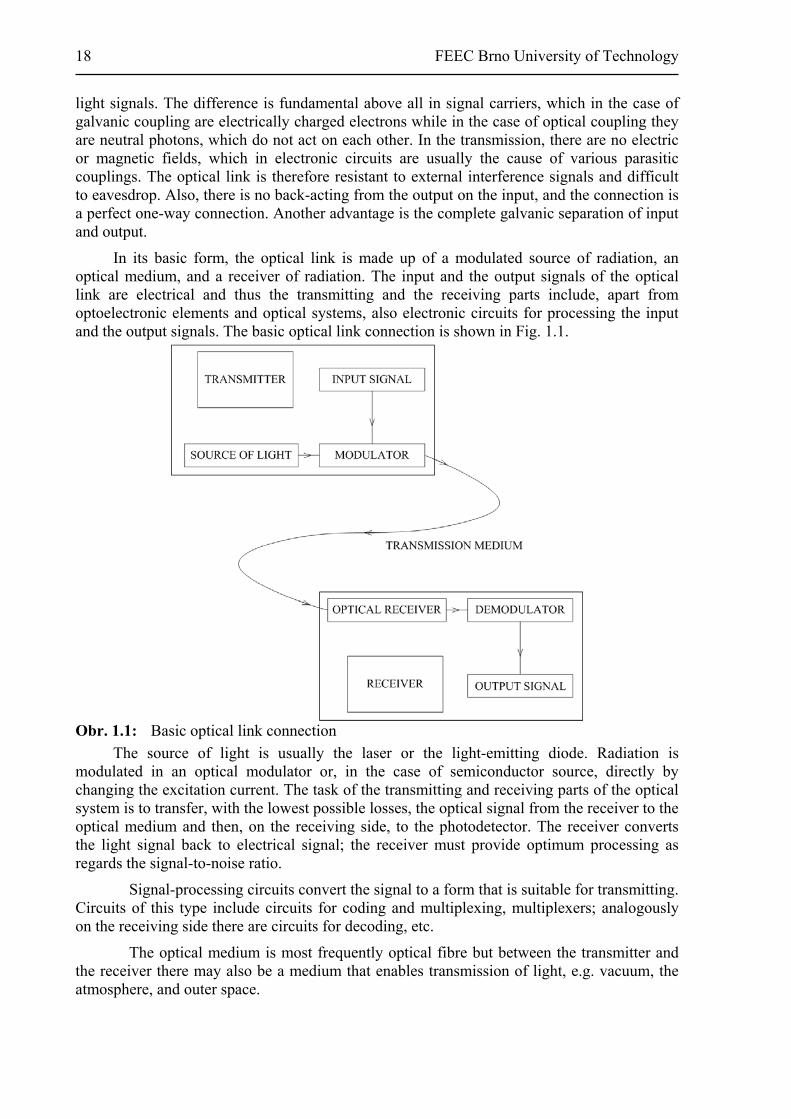
In its basic form, the optical link is made up of a modulated source of radiation, an optical medium, and a receiver of radiation. The input and the output signals of the optical link are electrical and thus the transmitting and the receiving parts include, apart from optoelectronic elements and optical systems, also electronic circuits for processing the input and the output signals. The basic optical link connection is shown in Fig. 1.1.
Obr. 1.1: Basic optical link connection
The source of light is usually the laser or the light-emitting diode. Radiation is modulated in an optical modulator or, in the case of semiconductor source, directly by changing the excitation current. The task of the transmitting and receiving parts of the optical system is to transfer, with the lowest possible losses, the optical signal from the receiver to the optical medium and then, on the receiving side, to the photodetector. The receiver converts the light signal back to electrical signal; the receiver must provide optimum processing as regards the signal-to-noise ratio.
Signal-processing circuits convert the signal to a form that is suitable for transmitting. Circuits of this type include circuits for coding and multiplexing, multiplexers; analogously on the receiving side there are circuits for decoding, etc.
The optical medium is most frequently optical fibre but between the transmitter and the receiver there may also be a medium that enables transmission of light, e.g. vacuum, the atmosphere, and outer space.
Optoelectronics for telecommunications and informatics 19
As mentioned above, the atmosphere is, from the viewpoint of reliability, not suitable for optical transmissions. During the passage of optical radiation through the atmosphere the radiation becomes attenuated due to absorption on the one hand and dispersion on the other. Selective absorption is caused by resonance bands of various gaseous components of the atmosphere such as water vapour, carbon dioxide, ozone, methane, carbon monoxide, and nitrogen oxides.
Besides absorption by gaseous components, radiation is also absorbed by aerosol particles present in the atmosphere. Radiation dispersion in the atmosphere is also caused by aerosol particles and by gas molecules.
The atmosphere is in most cases regarded as a non-homogeneous medium, in which differently heated strata get mixed randomly. The refractive index of air, which depends on temperature, acquires at different points different values of random nature, and it changes randomly with time. Passage through such a medium, which is referred to as turbulent medium, leads to fluctuations in the amplitude of light rays, impaired coherence, and increased beam divergence. These effects influence unfavourably the activity of optical signal receiver [1-2].
Flying birds (flocks of birds) have a very unfavourable effect on transmission, with the link being sometimes put completely out of operation. On the contrary, there is also something positive in that these transmissions do not require any frequency permits from the CTA (Czech Telecommunications Authority) as is the case with radio transmissions.
Transmission through outer space does not suffer from such problems and is used for transmissions between satellites.
Transmission over optical fibre is the most advantageous. Although the transmission does not suffer from such problems as in the case of atmospheric transmission, the parameters of the optical signal change in this transmission too. Pulses that are being transmitted become attenuated, their shape is changed and the time position may also be changed. The range can be increased by deploying repeaters, which may be either amplification or regenerative repeaters. In repeaters of the first type the signal is amplified, for example, in the optical band by a laser amplifier. The drawback is that noise increases and, consequently, the link quality decreases with increasing route length. Regenerative repeaters, in which the signal is restored to its initial quality, are based on digital transmissions and provide links whose quality does not depend on the link length.
The basic material used in the manufacture of optical fibres is SiO2 and numerous dopants, so-called alloying admixtures, such as GeO2, P2O5, B2O3, and others. Concentrating these dopants will yield the required properties as regards the magnitude and pattern of the refractive indices of the fibre core and cladding, which influences its transmission properties.
The technologies of manufacturing optical fibres have mostly a common principle and are based on the so-called preform. The preform is a glass rod, several decimetres long, whose cross-section represents an amplified profile of the fibre. After intensive heating, the fibre itself is drawn from the preform. The properties of the fibre produced depend on the preform quality and production precision. Demanding technological operations and procedures are concerned here.
Fibres of lower transmission properties can be manufactured by the original method of double crucible, in which the core and cladding materials are melted separately in a double crucible, from which the fibre proper is subsequently drawn. There is also another known method of manufacturing optical fibre, referred to as “rod in a tube”. The manufacture of fibres is dealt with in greater detail in Chapter 3.
20 FEEC Brno University of Technology
The transport properties of optical fibres depend on their design. We distinguish three basic types of design:
single-mode fibre with constant core refractive index,
multi-mode fibre with constant core refractive index,
fibre with variable core refractive index, which is often referred to as gradient-
index fibre.
The term mode is used here to denote one of physically admissible patterns of electromagnetic field distribution in the cross-section of the core of optical fibre. The modes form a series and there are a finite number of them. In multimode fibres, the number of propagating modes is of the order of hundreds to thousands. The number of propagating modes depends on fibre excitation. It is thus possible to excite just one mode. The manner of exciting the fibre affects its transmission properties; from this viewpoint, it is the single-mode fibres that exhibit the best transmission properties for long-haul transmissions.
The same as geometrical parameters, transmission properties are specified in ITU-T recommendations. These are: G 651 for gradient-index fibres, G 652 for single-mode fibres on the 1.3 µm wavelength, and G 653 for single-mode fibres on the 1.55 µm wavelength. The problematic of optical fibre radii is dealt with in the G 641 recommendation. A number of recommendations were drawn up on the problematic of building and installing cable routes with fibre-optic cables. All this standardization activity is under constant development [1-3].
If optical fibre is used as the transmission medium, there are several possibilities of combining radiation sources and detectors while maintaining mutual optical adaptation. For practical applications, light sources and detectors based on semiconductors are of particular importance. The basis is diode structures, in which emission of light is triggered by a process of recombining the carriers injected into the PN junction. Each recombination will produce a photon of light energy, whose wavelength depends on the dopant material. Stimulated emission in the Pn and GaAs junction was first observed in 1962. Advances in the technology did not take long in coming.
A great number of various types of semiconductor light-emitting (LED) and laser (LD) sources of light can be modulated directly and in a very simple way, by merely changing the current flowing through them. Light-emitting diodes, as sources of incoherent radiation, can be used to frequencies of up to 100 Hz; thus from the viewpoint of practice they can be used for links with lower demands on bandwidth and range. Laser diodes are the source of coherent radiation of a considerably greater optical power and can without major problems be modulated by frequencies above 1 GHz. They are used with advantage for long-haul links, where it is necessary to transmit a larger bandwidth, for multiplex transmissions, etc. Initial problems with the lifetime of laser sources have been resolved.
For the reverse conversion of radiation to electrical current we use photodetectors. The most advantageous for links with optical fibres are semiconductor diodes of the PIN type or avalanche photodiodes. The basic parameters that are decisive in the selection of photodetector are the highest transmitted frequency, the level of the transmitted signal, and the magnitude of the noise on the photodetector output. The solution of electronic circuits on the receiver side is, of course, of considerable effect on the quality of the whole transmission chain.
It is therefore obvious that choosing appropriately, from the viewpoint of power conditions, the transmitter and the receiver parts of the optoelectronic system the whole

Optoelectronics for telecommunications and informatics 21
system can be affected. Still, the key problem of the whole route design consists in the fibre’s own attenuation and dispersion.
The evolution of optoelectronic systems started from the first links realized over short distances; they were mostly data transmissions over short distances in interference environments, and many other industrial applications. They were followed by digital transmissions of the first and higher orders through optical cables, always in order to provide links between exchanges. Analogue transmissions were realized, too, be it FDM or image signal transmission. The development of optoelectronic telecommunication systems was greatly enhanced by the military’s interest in this new advanced technology.
With the perfection of the transmission parameters of optical fibres this new technology comes to be deployed on long-haul routes. In most of the cases realized, higher-order digital systems were deployed. Optical links are also finding their way into local networks. Various experimental routes have been realized, which enable greatly increasing the comfort of subscriber line (FTTH). A single optical fibre makes it possible for the subscriber to use voice, data and video services.
Optoelectronics has been found important for communication purposes and information transmissions in the area of railway management and power engineering.
Considerable success has been achieved in laying submarine optical cables. All the world oceans and seas are today intersected with optical cables.
In all these cases, links realized on the basis of optoelectronics greatly outdo links realized on the basis of classical metallic conductors for a number of reasons: the above advantages of optical transmission, and, in particular because of increased capacity due to the distance between regenerative repeaters increasing to over 50 km, easy installation, and, last but not least, replacement of the scarce copper. Obviously, the application of this new technology is also given by positive economic stimuli.
The decisive factor in the speed of the development of optoelectronic telecommunication systems and their application in practice is the development of the base of optoelectronic components. Worldwide, there are over one thousand manufacturers of optoelectronic components, inclusive of optical fibres and optical cables.
Research work concerned with problems of information transmission over optical fibres has been carried out systematically within fundamental and applied research in this country since 1975. This work was mainly focused on research and experimental verification of the manufacture of optical fibres, sources of infrared radiation, and fibre-fibre connectors. To assess the feasibility of introducing the manufacture of optoelectronic components in Czechoslovakia and start the development of optoelectronic telecommunication systems, a long-term programme of the development of optoelectronics in Czechoslovakia was launched in 1980.
In the years 1980 – 1984, some components enabling short-haul transmission of information over lightguides were developed and their manufacture was started. The respective methodology had been mastered and the manufacture of fast infrared transmission diodes connected to type PCS lightguides in several modifications was introduced. A fibre-fibre connector connected to PCS fibre and to optical cable containing this fibre was developed and introduced in practice. Also, a transmitter and receiver module with hybrid integrated circuits was developed that enabled transmitting digital signals at a rate of 10 Mbit.s-1 over a distance of 1000 metres using type PCS fibre, and over a distance of 2500 metres using type GI fibre. Fundamental research into planar components for the control of optical radiation on the principle of integrated optics was launched.

22 FEEC Brno University of Technology
The years 1985 – 1990 saw the development and gradual introduction into production of further components that enabled information transmission over longer distances along optical fibres of the telecommunication type. The fibre in question was of the GI type, manufacturer Sklo Union Teplice, and it was twisted into optical cables in Kablo Děčín. Various kinds of optical cable were manufactured, with a maximum of 12 fibres in a cable. The production started in 1989, with the production capacity greatly exceeding the demand. Also, the technology of semiconductor laser for the 0.85 μm and 1.3 μm bands connected to the GI lightguide was mastered and so was the manufacture of single-fibre optical connector for the GI fibre and for single-fibre optical cable, receiver diodes for the 1.3 μm band connected to the GI fibre. The development of the module of analogue signal transmitter and receiver with a bandwidth of up to 10 MHz was completed. The manufacturing technology of the avalanche photodiode for the 0.85 μm band connected to the fibre with connector was also mastered. This element was designed for plug-in units of receiver for the transmission of 2nd -order signals of digital systems.
In this period our first experimental route was put into operation in Prague. A 2nd-order digital system was deployed on a 4615 m long optical cable without repeaters. The optical cable was supplied by the company Sumitomo and the aim of the experiment was to test the installation and operation for further links under preparation. The system operates on the 0.85 μm wavelength; the fibre under testing provides good conditions for potential use also in the 1.3 μm band, where an attenuation of 0.4 dB . km-1 was measured, possibly also in the 1.55 μm band with an attenuation of ca. 0.37 dB . km-1. A gradual deployment was also prepared of further optical cables in local networks in Prague and Bratislava, and several other long-haul optical routes.
This brief listing might lead to the conclusion that the problematic of optical communications had been mastered. Unfortunately, the opposite was true. The state of optoelectronics in advanced countries remained elusive for us for over ten years.
The rapid development and significance of optoelectronics naturally had an impact on schools too. It is universities in particular that have participated and continue participating in the development of optoelectronics and its dissemination. In the first place, the departments of physics at universities have greatly contributed to the development of radiation sources and detectors. The production of our optical fibres has closely been connected with the research work of the Chemical-technological University in Prague. Numerous applications owe their origin to the workers and students of Electrical Engineering Faculties of the Czech Technical University in Prague, Brno University of Technology, Mining University in Ostrava, Slovak Technical University in Bratislava, Railway University in Žilina, etc.
In the telecommunications technology specializations the teaching of optoelectronics was first included as an addendum to the existing courses Telecommunication lines and Transmission systems. This was a logical follow-up to two classical technologies. With the continued rapid development of optoelectronics, separate courses such as Optoelectronics in telecommunications, etc. were included in the specialization streams.
The most advanced countries in this field include the USA, France, the UK, Japan, etc.
The current construction of optical networks and information systems in the Czech Republic is to a great extent based on the import of foreign technologies. Even if the optical cables are made in this country, the inside of cable core (the fibres) is from abroad. Systems and active elements are also mostly of foreign provenience. The production of “optics” in this country focuses on the production of components, connectors, converters, sources and detectors of radiation, splitters, and measuring devices. Tens of companies are engaged in the laying and maintenance of optical routes.

Optoelectronics for telecommunications and informatics 23
As an aside, it should be mentioned that in the former Czechoslovakia the technology of manufacturing the gradient-index multi-mode fibre had been mastered as well as the manufacture of the transmitter and receiver parts of digital systems. Although Czechs are world famous manufacturers of glass, manufacturing fibres for communication is a more demanding process, where it is necessary to constantly invest in the development, which only the richest countries of the world can afford.
Until 1990 there was an embargo on the export of optics to Czechoslovakia and this fact contributed to new networks being built with top-class optics and this has resulted in that telecommunications and information technology in the Czech Republic is on a very high level.
2 Transmission properties of optical fibres
The transmission properties of optical fibres depend in the first place on the type of fibre design. In this respect, three types of fibre are distinguished:
- multimode fibres with constant refractive index of the core and step refractive index of the jacket; these fibres are simple to manufacture and handle, and of a comparatively simple design but their drawback is greater attenuation and dispersion, and small transmission capacity. They feature large core and jacket diameters. An example of this type of fibre can be seen in Fig. 2.1.
Obr. 2.1: Multimode step-index fibre
Some characteristics of this type of fibre: Dj = 50 – 200 µm, Dp = 120 - 300 µm, dispersion 50 ns . km-1, attenuation 5 – 20 dB . km-1, and bandwidth 60 MHz.
Fibres of this type are mostly used in short-haul links, in particular for automation purposes, short data transmissions, local networks, etc.
Multimode fibres with varying refractive index in transversal section of the core, which feature lower dispersion, lower attenuation, somewhat more complicated manufacture and thus more complicated fibre design and splicing. The fibre has been standardized according to the ITU-T recommendation: Dj = 50 µm, Dp – 125 µm. An illustration of the refractive index pattern is given in Fig. 2.2.

24 FEEC Brno University of Technology
Obr. 2.2: Multimode fibre with varying refractive index
Some selected characteristics of this type of fibre are: dispersion at 0.85 µm is ca. 1 ns . km-1, attenuation 2.5 – 5 dB . km-1, transmitted bandwidth 600 MHz.
In view of the above parameters, this type of fibre is particularly suited for telecommunication purposes, namely for short-haul links.
Single-mode fibres with constant refractive index of the core and step refractive index of the jacket, which feature low dispersion, very low attenuation, and large transmission capacity. They mainly find application in long-haul transmissions. In this case there is only one mode propagating in the fibre, in the direction of the axis. To be able to achieve this state it is necessary to reduce the core diameter to a value equal to only a few light wavelengths. The diameter range is Dj = 7 - 9 µm, Dp = 125 µm, as shown in Fig. 2.3.
Obr. 2.3: Single-mode step-index fibre
Fibre characteristics: dispersion ca. 0.3 ns . km-1, attenuation below 0.2 dB . km-1 at a wavelength of 1.55 µm, and a bandwidth of 10 GHz.
In cases when the refractive index changes stepwise, the term layered lightguides is often used. In these cases the transmission is based on the principle of total refraction at the core-jacket interface. In the second type, the lightguide with continuously varying refractive index (so-called gradient-index lightguide), the path of the ray has the form of elliptic or circular helix.
Since the transmission properties of optical fibres depend on the pattern of refractive index distribution, various manufacturers apply further variants of different refractive index profiles, as illustrated in fig. 2.4.

Optoelectronics for telecommunications and informatics 25
Obr. 2.4: Examples of different refractive index profiles
Thus, for example, Fig. 2.4a illustrates a fibre lightguide that is used with success as an alternative to single-mode lightguides. Frequently occurring are two-layer lightguides and gradient-index lightguides with the curve of refractive index close to the parabolic curve. As will be given below, a more complicated pattern of refractive index can yield a shift in the dispersion characteristic, etc. [2-1], [2-2].
2.1 Attenuation of optical fibres
Attenuation of optical fibres is mainly due to:
- absorption by the medium in which the radiant energy is propagating,
- radiation from the fibre,
- diffusion on inhomogeneities.
Absorption losses in the UV and visible regions are due to the transitions between atomic levels and, in the infrared region, between molecular levels of the basic material, admixtures and impurities, of greatest effect among which are ions of Fe, Cu and Cr, whose resonance at certain frequencies is accompanied by thermal losses. The resonance frequency of OH ions, which represent the main part of the losses, corresponds to a wavelength of 2.8 µm so that it lies outside the band used for transmission over optical frequencies but the second harmonic, 1.38 µm, and the third harmonic, 0.94 µm, are in the band region that is used. Typical resonance curves due to OH ions are evident from Fig. 2.5. For the manufacture of fibres with low specific attenuation it is necessary to ensure a low concentration of OH ions and ions of metals.

26 FEEC Brno University of Technology
Radiation losses are due to the refraction of propagating rays on the interface of two dielectric mediums of different properties, when part of the energy escapes out of the core.
Dispersion losses are due to the fact that molecules randomly distributed in amorphous material actually form micro-inhomogeneities of the refractive index of the material. If these inhomogeneities and minor impurities are dimensionally small in comparison with the wavelength, the dispersion losses appearing on them are called Rayleigh’s scattering losses. The losses are inversely proportional to the fourth power of the wavelength of propagating radiation and they rapidly increase towards the UV region. The characteristic feature of Rayleigh’s scattering is its omnidirectionality.
From the practical viewpoint, the above losses can be extended with losses due to imperfect geometry, distorted shapes and dimensions of the boundary between the core and the cladding. Small cracks in the core material also play a role. Last but not least, the so-called microbends should be mentioned, which include defects in the rectilinearity of lightguide axis.
Obr. 2.5: Attenuation in fibre lightguides
Fig. 2.5 illustrates the losses described above and, at the same time, gives the development of the reduction of attenuation in fibre lightguides. In the most recently developed fibres the effect of OH ions has been eliminated, in particular between the 1.3 and 1.55 µm wavelengths, i.e. between the so-called 2nd and 3rd “windows”.
Attenuation, an important transmission quantity, can be defined as follows: Radiant power of wavelength λ at a distance z from the fibre beginning at an input power P (0, λ) is given by relation 2.1:
, 0, exp 2 . ,P z P x z dz (2.1)
where z , is the attenuation coefficient per unit of length, which can in general depend on the distance from the fibre beginning. It is therefore of advantage to introduce the average coefficient of fibre attenuation
1λ γ λ .
2z dz , (2.2 )

Optoelectronics for telecommunications and informatics 27
which simplifies dependence (2.1) to the approximate relation [2-3],
.exp,0, zPzP (2.3)
This relation is the starting point for measuring the attenuation of optical fibre by the differential method. When it is necessary to measure the transmitted power at two different points, we obtain from equation (2.3) the relations
.exp,0, 11 zPzP
2 2, 0, exp ,P z P z (2.4)
from which after rewriting we obtain the attenuation coefficient
..
.ln
1
2
1
12
zP
zP
zz (2.5)
The term derived shows that the average attenuation coefficient only depends on the ratio of input and output powers.
For practical reasons the attenuation coefficient is given in units of dB.km-1 according to the relation:
..
.log10
1
2
1
12
zP
zP
zz (2.6)
The methodology itself of measuring the attenuation will be described below. There are also other parameters that influence the attenuation characteristic. For example, in current operating conditions, changes in the temperature will not have any major effect on attenuation. In severe frost, however, some fibres will exhibit higher attenuation (at -30ºC ca. 2 dB.km-1). Attenuation also gets increased at higher positive temperatures, as shown in Fig. 2.6.
Obr. 2.6: Temperature dependence of lightguide attenuation
Fig. 2.7 illustrates what the attenuation pattern looks like in a fibre of “drowned” cable (i.e. a cable flooded with water) after eight months.

28 FEEC Brno University of Technology
Obr. 2.7: Dependence of attenuation of optical cable lightguide on λ after 8 months of cable “drowning”
In conclusion, let us sum up the knowledge gained about lightguide attenuation and current trends. Fig. 2.8 gives the attenuation characteristic with OH already eliminated on a wavelength of 1380 nm. At the same time, new wave windows are described.
1st window (850 nm) belongs to multimode propagation. Here, the attenuation characteristic is steeply falling and the achieved values of specific attenuation are too high to be used in long-haul transmissions in particular. Thanks to very cheap sources of radiation the transmission is used in optical access networks.
2nd window (1280 to 1335 nm) is the lowest and historically the first window that can fully be used for single-mode transmission over fibres with 9/125 µm diameters. The specific attenuation value achieved is typically just below 0.35 dB . km-1. This window is used for long-haul transmissions.
3rd window (1530 to 1565 nm) is a window in which the minimum specific attenuation appears for standard quartz fibre, typically in the range from 0.19 to 0.22 dB . km-1. This window is used for long-haul transmissions (transport and global networks).
4th window (1565 to 1625 nm) is already beyond the absolute minimum of specific attenuation. It is, however, so flat that the attenuation parameters differ only minimally from the 3rd window. It is the advances in the WDM technology and in optical amplifiers that allow, in the transmission of the joint spectrum of the 3rd and 4th windows, almost doubling the transmission capacity.
5th window (1335 to 1530 nm) has been available for transmission applications only since the late 1990s, when the technology of manufacturing optical fibres without OH admixtures was mastered to such a degree that the local maximum attenuation fades out at 1380 nm. Joint 2nd to 5th windows form a continuous transmission channel of 50 THz in bandwidth.
The current trend in transmission over optical fibre is characterized by a shift to the 2nd, 3rd, 4th and 5th windows, with single-mode lightguides being used. Today, the growth of these transmissions in comparison with multimode lightguides leads to reductions in their prices.
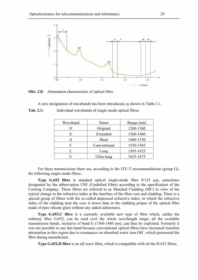
Optoelectronics for telecommunications and informatics 29
Obr. 2.8: Attenuation characteristic of optical fibre
A new designation of wavebands has been introduced, as shown in Table 2.1.
Tab. 2.1: Individual wavebands of single-mode optical fibres
Waveband Name Range [nm]
O Original 1260-1360
E Extended 1360-1460
S Short 1460-1530
C Conventional 1530-1565
L Long 1565-1625
U Ultra-long 1625-1675
For these transmissions there are, according to the ITU-T recommendations (group G), the following single-mode fibres:
Type G.652 fibre is standard optical single-mode fibre 9/125 µm, sometimes designated by the abbreviation USF (Unshifted Fibre) according to the specification of the Corning Company. These fibres are referred to as Matched Cladding (MC) in view of the typical change in the refractive index at the interface of the fibre core and cladding. There is a special group of fibres with the so-called depressed refractive index, in which the refractive index of the cladding near the core is lower than in the cladding proper of the optical fibre made of pure silicate glass without any added admixtures.
Type G.652.C fibre is a currently available new type of fibre which, unlike the ordinary fibre G.652, can be used over the whole wavelength range; all the available transmission bands, inclusive of band E (1360-1460 nm), can thus be exploited. Formerly it was not possible to use this band because conventional optical fibres have increased insertion attenuation in this region due to resonances on absorbed water ions OH-, which permeated the fibre during manufacture.
Type G.652.D fibre is an all-wave fibre, which is compatible with all the H.652 fibres.

30 FEEC Brno University of Technology
Type G.653 fibres have been developed with the aim of suppressing chromatic dispersions for the 1550 nm wavelength. These fibres are referred to as DSF (Dispersion Shifted Fibre) fibres. They are used for higher transmission speeds over great distances with a single wavelength in operation. However, when the need arose in practice to deploy systems of wavelength multiplex DWDM with several wavelengths, it was found that these fibres had a side effect. It consists in the overlapping of individual wavelengths and the appearance of parasitic neighbouring channels and cross-talk.
Type G.654 fibres have been developed as a special variant of the G.652 fibres. These fibres are optimized for the lowest possible insertion attenuation in the 1550 nm band and have the cut-off wavelength shifted (wavelength up to which they perform as single-mode fibres). They are expensive and are used almost exclusively for extreme long-haul transmissions over submarine cables without amplifiers along the route.
Type G.655 fibres with shifted non-zero dispersion (NZ-DSF, Non-Zero Dispersion Shifted Fibre) are optimized for the transmission region in the 1550 nm band. Today, these fibres are mainly used in wide-range optical networks; unlike type G.653 fibres, they do not have zero dispersion for the 1550 nm wavelength. Low non-zero dispersion is necessary lest non-linear side-effects should show here too much. This type of fibre is designed for the operation of DWDM technology and for high transmission speeds.
Type G.656 fibres with shifted non-zero dispersion (NZ-DSF, Non-Zero Dispersion Shifted Fibre) are optimized for the transmission region in the 1460-1625 nm band. These fibres are designed for the DWDM and CWDM wavelength multiplex systems. In the S band they enable up to 40 channels in the DWDM system. The maximum chromatic dispersion is set to be from 2 to 14 ps . nm/km-1, the maximum polarization dispersion is 0.20 ps √km.
Type G.657.A fibre is for inside/internal cabling and for optical access networks.
Type G.657.C fibre is a new type of fibre, which is resistant to microbending up to a radius of 5 mm.
When fibres are spliced, reflections appear on connectors and, generally, on all inhomogeneities in the fibre. This gives rise to random resonators of different frequencies, which can interfere with the performance of lasers and optical amplifiers or cause interferometric noise. The recommendations admit total route reflections of no more than -27 dB.
The behaviour of actual fibres may differ in dependence on the glass purity and dopants used but the characteristic behaviour on the respective wavelengths will prevail.
2.2 Dispersion in optical fibres
Dispersion in optical fibres is the main cause of distortion of the transmitted signal; it is defined as the difference of pulse width at half the height of the fibre at its beginning and end. The frequency dependence of refractive index, which gives rise to the frequency dependence of the group and phase velocities of wave propagation in the material of the lightguide, is the cause of material dispersion.
In the lightguide the material dispersion of the mode is combined with the waveguide dispersion, which is due to the changes in the mode geometry and thus also changes in the group and phase velocities of propagation when the frequency changes. The resultant effect of material and waveguide dispersions is usually referred to as chromatic dispersion.
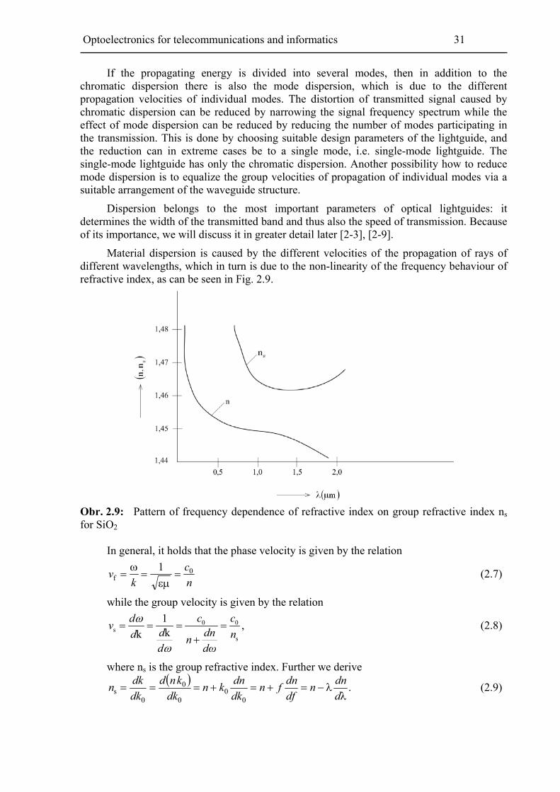
Optoelectronics for telecommunications and informatics 31
If the propagating energy is divided into several modes, then in addition to the chromatic dispersion there is also the mode dispersion, which is due to the different propagation velocities of individual modes. The distortion of transmitted signal caused by chromatic dispersion can be reduced by narrowing the signal frequency spectrum while the effect of mode dispersion can be reduced by reducing the number of modes participating in the transmission. This is done by choosing suitable design parameters of the lightguide, and the reduction can in extreme cases be to a single mode, i.e. single-mode lightguide. The single-mode lightguide has only the chromatic dispersion. Another possibility how to reduce mode dispersion is to equalize the group velocities of propagation of individual modes via a suitable arrangement of the waveguide structure.
Dispersion belongs to the most important parameters of optical lightguides: it determines the width of the transmitted band and thus also the speed of transmission. Because of its importance, we will discuss it in greater detail later [2-3], [2-9].
Material dispersion is caused by the different velocities of the propagation of rays of different wavelengths, which in turn is due to the non-linearity of the frequency behaviour of refractive index, as can be seen in Fig. 2.9.
Obr. 2.9: Pattern of frequency dependence of refractive index on group refractive index ns for SiO2
In general, it holds that the phase velocity is given by the relation
n
c
kv 0
f1
(2.7)
while the group velocity is given by the relation
0 0s
s
1,
kk
c cdv
d dnd nnd dω
(2.8)
where ns is the group refractive index. Further we derive
.0
00
0
0s
d
dnn
df
dnfn
dk
dnkn
dk
knd
dk
dkn (2.9)
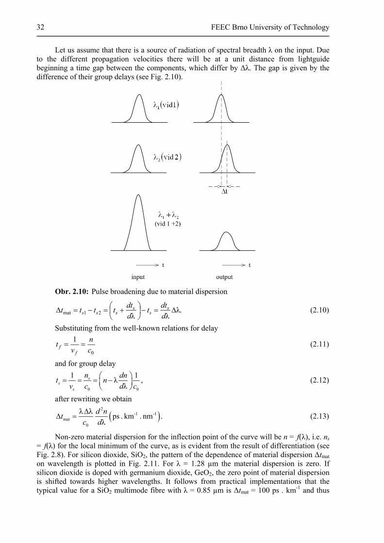
32 FEEC Brno University of Technology
Let us assume that there is a source of radiation of spectral breadth λ on the input. Due to the different propagation velocities there will be at a unit distance from lightguide beginning a time gap between the components, which differ by Δλ. The gap is given by the difference of their group delays (see Fig. 2.10).
Obr. 2.10: Pulse broadening due to material dispersion
.λλλ21mat
d
dtt
d
dttttt s
ss
sss (2.10)
Substituting from the well-known relations for delay
0
1
c
n
vt
ff (2.11)
and for group delay
0 0
1 1λ ,
λs
ss
n dnt n
v c d c
(2.12)
after rewriting we obtain
2
-1 -1mat
0
λ λps . km . nm .
λ
d nt
c d
(2.13)
Non-zero material dispersion for the inflection point of the curve will be n = f(λ), i.e. ns = f(λ) for the local minimum of the curve, as is evident from the result of differentiation (see Fig. 2.8). For silicon dioxide, SiO2, the pattern of the dependence of material dispersion Δtmat on wavelength is plotted in Fig. 2.11. For λ = 1.28 µm the material dispersion is zero. If silicon dioxide is doped with germanium dioxide, GeO2, the zero point of material dispersion is shifted towards higher wavelengths. It follows from practical implementations that the typical value for a SiO2 multimode fibre with λ = 0.85 µm is Δtmat = 100 ps . km-1 and thus

Optoelectronics for telecommunications and informatics 33
laser with a spectral breadth of 3 nm will cause a material dispersion of 300 ps . km-1 in the lightguide.
Obr. 2.11: Dependence of material dispersion on λ, for SiO2
Waveguide dispersion is also responsible for broadening the pulses transmitted by lightguides. This is because the propagation constant is different for every mode so that its frequency is changed, which results in a change of the speed of propagation. In multimode lightguides with step- and gradient-index profiles the effect of waveguide dispersion can be neglected. It must, however, be taken into consideration in single-mode fibres, where it has a substantial share in the total dispersion of this fibre. For a wavelength of 1.3 µm the dispersion value is around 2 ps . km-1.
Dimensionless waveguide dispersion coefficient Dwav comes to be introduced as the measure of waveguide dispersion:
s0 1 ,v1n s
dTD c f t
df (2.14)
where 101s1s . cnt is the group delay of the wave propagating in the lightguide axis,
with group refractive index 1111 ., sssss tttTn is the normalized group delay
Chromatic dispersion, which is formed by material and waveguide dispersions, is thus due to the non-linear frequency dependence of the group velocity of mode propagation in the lightguide. The bandwidth of the lightguide is inversely proportional to the bandwidth of the radiation source. For example, a semiconductor laser with the typical value of relative spectral breadth Sz.f0
-1 = 0.0001 enables transmitting a 400 times broader band than a light-emitting

34 FEEC Brno University of Technology
diode (LED) with a typical relative spectral breadth of 0.04. The chromatic dispersion coefficient is defined as
.s0chr df
dtfcD (2.15)
It is possible to choose for the lightguide such an operating frequency that chromatic dispersion in the middle of the transmitted band is zero. A practical consequence in the single-mode SiO2 fibre is the shifting of the operating mode from the 1.28 µm wavelength, at which the material dispersion is zero, to a wavelength of ca. 1.33 µm, where the chromatic dispersion is zero. In this way, the transmitted band of single-mode lightguides can be extended.
Mode dispersion is the main factor that limits the width of transmitted band in multimode lightguides with homogeneous core. For these lightguides, the mode dispersion can be explained using the method of geometrical optics. The larger the angle between the ray trajectory and the lightguide axis (the higher the mode), the longer the path between the lightguide input and output; the ray’s longitudinal velocity in the lightguide axis direction is lower. This is the reason why higher modes, which are closer to their cut-off frequencies, propagate more slowly than lower modes do. At a unit distance from the lightguide beginning there will be a time gap between individual modes, which will be given by their group delays. For a mode propagating in the lightguide axis and a mode whose trajectory contains an angle with the axis it holds
.1cos 0
ss
2
1ss
svid
c
nt
n
ntt
tt (2.16)
In gradient-index lightguides the ratios are better. With optimum profile of the refractive index the magnitudes of the mode and the material dispersions are of the same order and it holds
.1
21
10
0vid
c
nt (2.17)
The typical value for multimode step-index fibre is 20 ns . km-1, which allows transmitting bandwidths of up to tens of MHz . km; for gradient-index fibre it is 50 ps . km-1 with bandwidths of units of GHz . km while for single-mode fibre the dispersion is almost zero and the bandwidth is up to ca. 200 GHz . km. The concrete value of mode dispersion for gradient-index fibre and parabolic profile of refractive index of n(0) = 1,51, and n(a) = 1,5 is
111vid t ps . km-1.
The total number of propagating modes in gradient-index fibre lightguide is given by the relation
2 20 .
2M a k
e
(2.18)
For the parabolic profile of refractive index 2 the number of propagating modes is half the number of modes for the gradient-index profile of two-layer lightguide with homogeneous core , with identical values of a, Δ. For example, for the parabolic profile with the parameters ,2 n(0) = 1,51, n(a) = 1,5, λ = 0,84 μm, a = 80 μm and the total number of propagating modes is M = 1040.
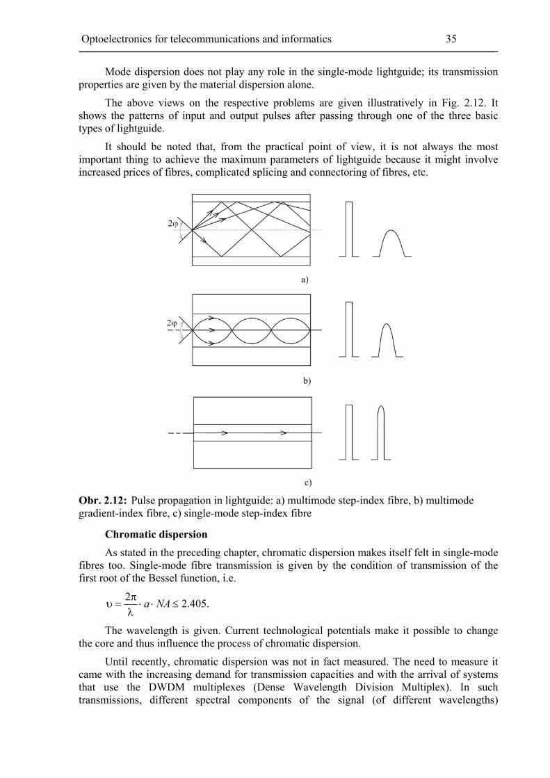
Optoelectronics for telecommunications and informatics 35
Mode dispersion does not play any role in the single-mode lightguide; its transmission properties are given by the material dispersion alone.
The above views on the respective problems are given illustratively in Fig. 2.12. It shows the patterns of input and output pulses after passing through one of the three basic types of lightguide.
It should be noted that, from the practical point of view, it is not always the most important thing to achieve the maximum parameters of lightguide because it might involve increased prices of fibres, complicated splicing and connectoring of fibres, etc.
Obr. 2.12: Pulse propagation in lightguide: a) multimode step-index fibre, b) multimode gradient-index fibre, c) single-mode step-index fibre
Chromatic dispersion
As stated in the preceding chapter, chromatic dispersion makes itself felt in single-mode fibres too. Single-mode fibre transmission is given by the condition of transmission of the first root of the Bessel function, i.e.
.405.22
NAa
The wavelength is given. Current technological potentials make it possible to change the core and thus influence the process of chromatic dispersion.
Until recently, chromatic dispersion was not in fact measured. The need to measure it came with the increasing demand for transmission capacities and with the arrival of systems that use the DWDM multiplexes (Dense Wavelength Division Multiplex). In such transmissions, different spectral components of the signal (of different wavelengths)

36 FEEC Brno University of Technology
propagate simultaneously through the optical fibre at different velocities. The signal always contains several spectral components. In this case some components of the input signal pulse will be time-delayed when passing through the optical fibre. Due to the passage through optical fibre the pulse will extend in time and this deformed pulse will get into the neighbouring bit gaps and the transmitted information will be distorted. The magnitude of chromatic dispersion is characterized by the so-called chromatic dispersion coefficient
λ
λ ,λ
gd tD
d
which gives the change of the group delay tg of a signal passing through the fibre, in dependence on wavelength λ. The maximum values of chromatic dispersion coefficient according to ITU-T G.695 are given in Table 2.2. The coefficient value gives the extension of the (Gaussian) pulse in ps for a radiation source of 1 nm spectral half-width, after passing through a 1 km fibre.
Tab. 2.2: Limit values of chromatic dispersion according to ITU-T G.695
Wavelengths λ [nm] Chromatic dispersion coefficient D (λ) [ps.nm-1.km-1]
1291-1351 5,7
1311-1371 6,8
1391-1451 11,5
1531-1591 19,9
1471-1611 21,1
Obr. 2.13: Pattern of chromatic dispersion of conventional fibre
A classical pattern of chromatic dispersion is given in Fig. 2.13. As mentioned above, the fibre can be prepared technologically such that also in the wavelength region 1.55 µm the dispersion values are reduced to zero. These cases of DS (Dispersion Shifted) fibres are given

Optoelectronics for telecommunications and informatics 37
in Fig. 2.14; a) concerns the so-called fibre with shifted dispersion characteristic while b) concerns the fibre with flat dispersion characteristic.
Obr. 2.14: Pattern of chromatic dispersion in fibres with shifted dispersion characteristic
The arrival of DWDM has entailed the problem of how to compensate chromatic dispersion in older, already installed fibres. Most frequently, passive optical compensation is used, which employs special compensation fibres DCF (Dispersion Compensation Fibre) of high negative chromatic dispersion value. The method consists in connecting a “coil” of this fibre at the end of the route (about 1/6 of the actual length) and this will compensate the dispersion value. Examples of route compensation are given in Figs 2.15 and 2.16.
Obr. 2.15: Example of chromatic dispersion compensation of optical route
Obr. 2.16: Example of PMD - polarization mode dispersion
Today, new types of compensation fibres are available, with sufficient negative slope of the dispersion characteristic, suitable for the compensation of conventional and NZDF (Non

38 FEEC Brno University of Technology
Zero Dispersion Fibre) fibres. This compensation can also be achieved using the special HOM (High Order Mode) multimode fibres. Moreover, the chromatic dispersion of these HOM fibres is ca. three times higher than in classical DCF fibres so that it suffices to use only a third of the length of compensation fibre in comparison with the DCF fibre. HOM fibres have a low specific attenuation and are resistant to non-linear events. Another compensation possibility consists in using the Bragg gratings. Such a grating with varying grating period can be used for a function similar to compensation fibre, but usually for only a narrow spectral region of a few nm (up to ca. 6 nm). To compensate the chromatic dispersion of several spectral channels it is in this case necessary to employ a cascade of such gratings. Today, of course, wide-spectrum compensators with the Bragg gratings are available for bands of up to 35 nm.
A typical, practically applied fix compensator of chromatic dispersion for high-speed optical networks, based on the Bragg grating technology, can be used for single-channel or broadband transmission, either in real time or for static compensation.
Typical properties:
- it compensates one or several channels simultaneously,
- insertion attenuation is less than 3.5 dB,
- it balances the slope of the dispersion curve of transmission fibre,
- it has small dimensions.
Typical applications:
- as an alternative to dispersion compensation fibre DCF,
- in metropolitan and long-haul DWDM networks,
- SSSDH/SONET and CATV transmission routes,
- compensation at terminal or transmission point of transmission route,
- correction of residual chromatic dispersion and dispersion curve slope.
Polarization mode dispersion (PMD)
With the transmission speeds in individual optical fibres increasing to over 2.5 Gb/s the need to measure PMD has increased. When passing through the optical fibre, the mode propagates in two mutually perpendicular planes. This phenomenon deteriorates with any circular asymmetry of optical fibre; this may be due, for example, to microbends formed in the course of installation or directly to the manufacture or faulty installation of the cable, on which all sorts of external pressure then act. All this can result in that the two polarizations propagate at different rates and thus in signal distortion or pulse widening.
The polarization mode dispersion is expressed by the PDM coefficient. Over short distances, approximately to 10 km, PMD is roughly linear and is expressed by
1PMD ps.km ,L
(2.19)
where L – is the length of route, Δ τ – is the signal delay. Over long distances it does not propagate linearly but with the square root of the distance
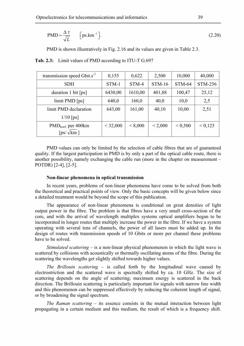
Optoelectronics for telecommunications and informatics 39
1PMD ps.km .L
(2.20)
PMD is shown illustratively in Fig. 2.16 and its values are given in Table 2.3. Tab. 2.3: Limit values of PMD according to ITU-T G.697
transmission speed Gbit.s-1 0,155 0,622 2,500 10,000 40,000
SDH STM-1 STM-4 STM-16 STM-64 STM-256
duration 1 bit [ps] 6430,00 1610,00 401,88 100,47 25,12
limit PMD [ps] 640,0 160,0 40,0 10,0 2,5
limit PMD declaration
1/10 [ps]
643,00 161,00 40,10 10,00 2,51
PMDkoef. per 400km
[ps/ km ]
< 32,000 < 8,000 < 2,000 < 0,500 < 0,125
PMD values can only be limited by the selection of cable fibres that are of guaranteed quality. If the largest participation in PMD is by only a part of the optical cable route, there is another possibility, namely exchanging the cable run (more in the chapter on measurement – POTDR) [2-4], [2-5].
Non-linear phenomena in optical transmission
In recent years, problems of non-linear phenomena have come to be solved from both the theoretical and practical points of view. Only the basic concepts will be given below since a detailed treatment would be beyond the scope of this publication.
The appearance of non-linear phenomena is conditional on great densities of light output power in the fibre. The problem is that fibres have a very small cross-section of the core, and with the arrival of wavelength multiplex systems optical amplifiers began to be incorporated in longer routes that multiply increase the power in the fibre. If we have a system operating with several tens of channels, the power of all lasers must be added up. In the design of routes with transmission speeds of 10 Gbits or more per channel these problems have to be solved.
Stimulated scattering – is a non-linear physical phenomenon in which the light wave is scattered by collisions with acoustically or thermally oscillating atoms of the fibre. During the scattering the wavelengths get slightly shifted towards higher values.
The Brillouin scattering – is called forth by the longitudinal wave caused by electrostriction and the scattered wave is spectrally shifted by ca. 10 GHz. The size of scattering depends on the angle of scattering; maximum energy is scattered in the back direction. The Brillouin scattering is particularly important for signals with narrow line width and this phenomenon can be suppressed effectively by reducing the coherent length of signal, or by broadening the signal spectrum.
The Raman scattering – its essence consists in the mutual interaction between light propagating in a certain medium and this medium, the result of which is a frequency shift.

40 FEEC Brno University of Technology
Scattered light wave propagates in both directions. Critical power depends again on the material and on the number, average output power and mutual spacing of optical channels. A practical application of the Raman phenomenon had to be waited for till the mid 1980s, when research into stimulated Raman phenomenon led to its practical deployment as an amplification element in the medium of single-mode fibres.
Own phase modulation – is the result of the optical pulse acting on itself. The increase and decrease of power on the edges of optical pulse lead to changes in its propagation phase and thus to its shape being distorted and its spectrum being broadened; in a dispersion medium the spectrum can retroactively affect the pulse shape. With excessive pulse broadening the pulses overlap in intersymbol interference and, subsequently, transmission errors occur.
Cross phase modulation – is in principle a phenomenon similar to own phase modulation but in conditions when the signal of one wavelength modulates the signal of another wavelength. Therefore it only appears in multichannel optical systems.
Four-wave mixing – is a non-linear phenomenon where the interaction of signals of two or more wavelengths gives rise to signals of new wavelengths. It is similar to the electrotechnical effect where intermodulation products arise during modulation [2-6].
2.3 Zheory of transmission over lightguides
In any real transmission medium, thus in lightguides too, the signal gets distorted. The distortion is due to two basic causes. On the one hand, it is the irregularity of the frequency response of the fibre itself, which is responsible for the change in the spectrum and time behaviour of the signal. The other cause of the distortion and impaired propagation capacity of the signal is noise.
The level of lightguide noise is determined from the power on the input. Most important is quantum noise, with thermal noise also playing a role.
An analysis of propagation is very complicated, in multimode lightguides in particular. The aim of the analysis is to determine the pulse of transition function of the lightguide or the frequency response
exp j .K K (2.21)
Based on the knowledge of these characteristics the shape of the output signal can be found in dependence on the input signal. In practical cases and in the optical fibre transmission mode we are mostly not interested in the exact shape of the output signal but only in its elongation in comparison with the input signal. This enables determining the parameter of optical communication route – the transmission speed or the width of transmitted band.
The frequency response is determined in the modulation frequency spectrum ω = 2 π fm and it is
2 2 1 1exp j / exp j ,K P P (2.22)
where P1(ω) and P2(ω) are the input and output powers. The absolute value
12 / PPK (2.23)
is the frequency response, and
Optoelectronics for telecommunications and informatics 41
12 (2.24)
is the amplitude characteristic. It is of advantage to normalize the amplitude characteristic such that
0 1.n
K (2.25)
In this case we are concerned with normalized amplitude characteristic.
The width of the pass-band is determined by the drop of amplitude characteristic by 3 dB, or the drop of normalized characteristic to the value 0.5
0,5.n
K (2.26)
The starting point of measuring is the frequency fm = 0 and the band is denoted as width S. The relation between input signal P1(t) and output signal P2(t) is given by the relation
2 1 ,P K P (2.27)
where P1(ω) and P2(ω) are the Fourier images of the input and output signals P1(t) and P2(t), where
.tjexp dtωtPP (2.28)
The output signal P2(t) is obtained by performing the transformation of the signal P1(t). Multiplying the obtained input signal image P1(ω) by the function K(ω) yields the output signal image P2(ω). Reverse transformation according to the relation
1exp j d ,
2P t P t
(2.29)
gives the output signal P2(t). In the majority of practical cases the integration must be performed numerically. With regard to the usual transmission mode the analysis of the transmission signals is the most important. The characteristic of the response to the input signal in the form pulse can be used to calculate the response to the input signal of any arbitrary form. The best method of examining the transmission properties of lightguides is to use a pulse in the shape of Gaussian curve or the Dirac pulse, denoted δ function; the Dirac pulse is in practice realized by a very short rectangular pulse. Using the Dirac pulse enables determining the width of the transmitted band. Denoting the Dirac pulse P1i(t), its Fourier image is
li 1i exp j exp j 1.P P t t dt t dt
(2.30)
The image of the response to the Dirac pulse is
.12 KPKP ii (2.31)

42 FEEC Brno University of Technology
Obr. 2.17: Lightguide transmission of signals: a) normalized characteristic, b) response to the Dirac pulse
The input signal as a response to the unity pulse is
.tjexpt2 ωdωKP i
(2.32)
The response to the unity pulse on the lightguide input is thus given by the reverse transformation of the frequency response. It is apparent that the lower the P2i(t) curve on the prescribed level, the wider the pass-band of the lightguide. The response to unity pulse is called the pulse response. Its qualitative evaluation is done by determining its width τ on the level of half the amplitude. This problematic is made clear in Fig. 2.17. It can be proved that the product S . τ depends only very little on the concrete shape of frequency response and is within the bounds
.6,045,0 S (2.33)
The speed of information transmission C is given in bits per second and in the digital transmission of binary signals it is numerically approximately equal to the maximum modulation frequency fm max, which is close to the width of transmitted band. Thus we have
SfC maxm (2.34)
a
0, 45 0,6.C
(2.35)
Relation (2.35) is used to estimate the transmission speed but, of course, on the assumption that the value of τ is known. It is evident from the above that the basic problem in determining the width of lightguide pass-band or the transmission speed is the determination of the frequency response. It can be established either by measurement or by calculation.
Direct measurement of the lightguide frequency response is complicated. Such a measurement requires exciting successively individual modes on the input and determining

Optoelectronics for telecommunications and informatics 43
their frequency responses or exciting the whole spectrum of modes with uniform power distribution among individual modes.
It is simpler to measure the frequency response of a system made up of lightguide source and detector. In this case it suffices to have at one’s disposal a frequency-tuned source of optical radiation and a detector with a known voltage dependence of emitted or incident power. The frequency responses can be used only for the source and detector with which the measurement was carried out.
The frequency characteristic can also be established indirectly, by measuring the response to the Dirac pulse and its reverse Fourier transform. Also in this case, however, it is necessary for the energy of input pulse to be distributed exactly and definably into individual modes.
The frequency responses measured can be used to determine the response to an arbitrary input signal and the width of transmitted band but this will not reveal the connection with the lightguide design parameters.
To propose an optimum lightguide design it is necessary to know the dependence of frequency response on design parameters. Such dependence can only be established via calculation starting from the fact that the shape of frequency response is in direct relation to chromatic and mode dispersions. The calculation is therefore closely linked with a detailed examination of the theory of the mechanism of originating individual dispersions.
The analysis of the propagation over real lightguides resulted in the following possible widths of the transmitted band:
- multimode lightguide with constant refractive index of the core and wit arbitrary source of radiation 10 < S < 15 [MHz . km]
- gradient-index lightguide with semiconductor laser operating at non-optimum frequency (with respect to material dispersion) 10 < S < 2000 [MHz . km]
- gradient-index lightguide with semiconductor laser operating at optimum frequency 0.2 < S < 10 [GHz . km]
- single-mode lightguide with constant refractive index of the core with semiconductor laser operating at optimum frequency S of up to 1000 [GHz . km].
It is obvious from the above data that the development in optical transmission over longer distances will take the path of introducing single-mode optical fibres.
Problems of energy propagation in optical fibres can be solved by two approaches: either on the basis of geometrical optics or on the basis of wave optics. Geometrical optics gives clear and simple results but they are valid only in the first approximation. The results are suitable above all for multimode fibres and their physical interpretation is easy but does not give a complete picture of the processes in the fibre.
Wave optics gives results that are more exact. However, their physical interpretation is more difficult and frequently the relations derived cannot be solved analytically. A clear picture can be obtained of field distribution in both the transverse and the longitudinal directions, and conditions of the propagation of individual components can be derived.
Geometrical optics of transversely homogeneous fibres. Geometrical optics starts from the assumption that light energy propagates in the medium along certain curves, the light rays. At the same time it assumes that the wavelength of propagating energy is negligibly short (λ→0). The ideal fibre, i.e. fibre without interference, is considered as the model. Its effect on
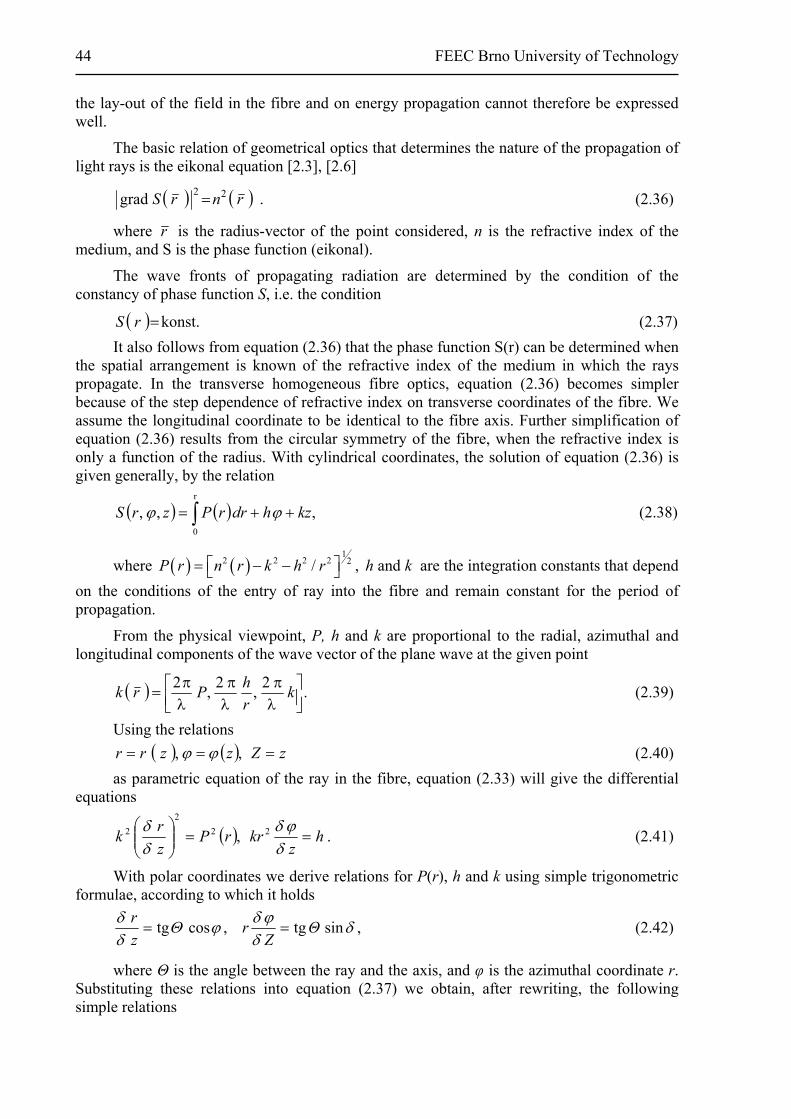
44 FEEC Brno University of Technology
the lay-out of the field in the fibre and on energy propagation cannot therefore be expressed well.
The basic relation of geometrical optics that determines the nature of the propagation of light rays is the eikonal equation [2.3], [2.6]
.grad 22rnrS (2.36)
where r is the radius-vector of the point considered, n is the refractive index of the medium, and S is the phase function (eikonal).
The wave fronts of propagating radiation are determined by the condition of the constancy of phase function S, i.e. the condition
.konstrS (2.37)
It also follows from equation (2.36) that the phase function S(r) can be determined when the spatial arrangement is known of the refractive index of the medium in which the rays propagate. In the transverse homogeneous fibre optics, equation (2.36) becomes simpler because of the step dependence of refractive index on transverse coordinates of the fibre. We assume the longitudinal coordinate to be identical to the fibre axis. Further simplification of equation (2.36) results from the circular symmetry of the fibre, when the refractive index is only a function of the radius. With cylindrical coordinates, the solution of equation (2.36) is given generally, by the relation
r
0
,,, kzhdrrPzrS (2.38)
where 1
2 2 2 2 2/ ,P r n r k h r h and k are the integration constants that depend
on the conditions of the entry of ray into the fibre and remain constant for the period of propagation.
From the physical viewpoint, P, h and k are proportional to the radial, azimuthal and longitudinal components of the wave vector of the plane wave at the given point
.2
,2
,2
kr
hPrk (2.39)
Using the relations
zZzzrr ,, (2.40)
as parametric equation of the ray in the fibre, equation (2.33) will give the differential equations
., 22
2
2 hz
krrPz
rk
(2.41)
With polar coordinates we derive relations for P(r), h and k using simple trigonometric formulae, according to which it holds
,sintg,costg
ΘZ
rz
r (2.42)
where Θ is the angle between the ray and the axis, and φ is the azimuthal coordinate r. Substituting these relations into equation (2.37) we obtain, after rewriting, the following simple relations
Optoelectronics for telecommunications and informatics 45
12 2
2 22
,
sin sin ,
cos ,
hP r n r k
r
h n r r
k n r
(2.43)
which enable classifying the rays into sets by the parameters h and k and in dependence on the conditions of the entry of rays into the fibre, i.e. in dependence on the angles φ, Θ, on radius r and on the value of refractive index at the point of entry n(r). The term that determines the value P(r) can be real positive or negative. The former corresponds to guided waves, the latter to decaying waves. Geometrical optics is only concerned with guided waves.
The preceding relations make it possible to assume that rays propagate in the fibre as a result of reflections on the interface of two mediums of different refractive index values. The relation between incidence angle Θ1 and refraction angle ΘR is given by the Snell law
.sinsin 21 Ri ΘnΘn (2.44)
The total reflection of ray on the interface occurs when sin ΘR = 1, from which it follows
.sin1
2
n
nΘi (2.45)
The maximum angle (with respect to the fibre axis), at which rays can enter the fibre and propagate in it, is defined by the so-called numerical aperture (NA). This dependence is expressed by the relation
2 2max 1 2NA sin .n n (2.46)
Geometrical optics gives a simple but only approximate relation for the dispersion of guided rays.
Wave optics of transversely homogeneous fibres starts from the solution of Maxwell’s equations. With a view to the fibre geometry, it is of advantage to solve the equation in cylindrical coordinates. The solution of these equations enables finding the spatial arrangement of the electromagnetic field inside and outside the core, and determining the propagation conditions for individual modes of the electromagnetic field. The exact solution of Maxwell’s equations is known and so is the solution under simplifying assumptions and with the introduction of linear polarized modes, inclusive of relations with the components of electromagnetic field.
An analysis of electromagnetic field using linearly polarized modes (LP modes) is simpler than a description using the electromagnetic field components. The derived results make it also possible to assign the denotation of electromagnetic field components (TM, TE, EH, HE) to the corresponding denotation in the terminology of linear polarized modes. On the basis of the derivation (see [2-3]) a simple form of the dispersion equation of LP modes can be obtained
1 1 ,l l
l l
J u K wu w
J u K w (2.47)
which is in agreement with the dispersion equation derived via simplified solution of Maxwell’s equations. For dimensionless parameters it holds that the critical values of the constant of propagation in the direction of axis z are equal to n2k while the parameter w is in that case equal to zero. Under these conditions, dispersion equation (2.47) will be fulfilled only for J1-1(u) = 0. From this value we can determine the values of argument u that
46 FEEC Brno University of Technology
corresponds to the critical values of the constant β and the denotation of linear polarized modes. The roots of Bessel functions J1(u) and J0(u) correspond to the following denotation of linear polarized modes. For J1(u) and arguments u = 0 and 3.85 the corresponding modes are LP01 and LP02. For J0(u) = 0 and arguments u = 7.015, 2.40, 5.52 and 8.67 the corresponding modes are LP03, LP11, LP12, and LP13.
Obr. 2.18: Curves for Bessel functions Jo and Je and propagation boundaries of corresponding modes
When the condition 0 < u < 2.4 is fulfilled, only one transverse mode LP01 will
propagate through the fibre. Fig. 2.18 gives the curves of Bessel functions J0 and J1 in dependence on the value of argument u, together with the regions beginning from which the respective LP mode can propagate.
The propagation constant will be determined from the relation
,1/ 2 bnkβ (2.48)
where
.a/12
2122
n
nnvub
(2.49)

Optoelectronics for telecommunications and informatics 47
Obr. 2.19: Propagation constant β in dependence on normalized frequency
Propagation constants for various field lay-outs are illustrated in Fig. 2.19. The direct detection of light signals distinguishes only the envelope delay caused by the change in group velocity, which is given by the relation
.sk kd
βd
c
Lτ (2.50)
When differentiating relation (2.48), the dependence of n, Δ and b on the wave vector k must be respected. With small differences between the refractive indices of the core and the cladding, Δ does not depend on k, and for the majority of materials used for fibres it holds
.nkd
ndk (2.51)
Respecting these relations, we obtain the group velocity
.sk
kd
kbdn
kd
knd
c
Lτ (2.52)
The wave vector k can be expressed by the relation
.
21
22
21 nna
vk
(2.53)
Relation (2.52) can then be rewritten in the form
.sk
vd
vbdn
kd
knd
c
Lτ (2.54)
The first part of this term characterizes the material dispersion, which is the same for all modes. The second part expresses the mode delay due to waveguide dispersion. Of decisive effect in this term is the coefficient d(bv)/dv, which after modification can be written in the form
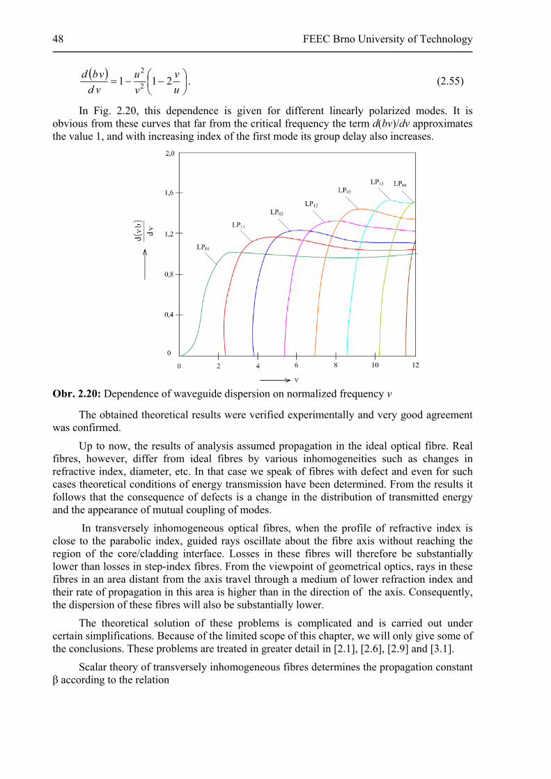
48 FEEC Brno University of Technology
.211 2
2
u
v
v
u
vd
vbd (2.55)
In Fig. 2.20, this dependence is given for different linearly polarized modes. It is obvious from these curves that far from the critical frequency the term d(bv)/dv approximates the value 1, and with increasing index of the first mode its group delay also increases.
Obr. 2.20: Dependence of waveguide dispersion on normalized frequency v
The obtained theoretical results were verified experimentally and very good agreement was confirmed.
Up to now, the results of analysis assumed propagation in the ideal optical fibre. Real fibres, however, differ from ideal fibres by various inhomogeneities such as changes in refractive index, diameter, etc. In that case we speak of fibres with defect and even for such cases theoretical conditions of energy transmission have been determined. From the results it follows that the consequence of defects is a change in the distribution of transmitted energy and the appearance of mutual coupling of modes.
In transversely inhomogeneous optical fibres, when the profile of refractive index is close to the parabolic index, guided rays oscillate about the fibre axis without reaching the region of the core/cladding interface. Losses in these fibres will therefore be substantially lower than losses in step-index fibres. From the viewpoint of geometrical optics, rays in these fibres in an area distant from the axis travel through a medium of lower refraction index and their rate of propagation in this area is higher than in the direction of the axis. Consequently, the dispersion of these fibres will also be substantially lower.
The theoretical solution of these problems is complicated and is carried out under certain simplifications. Because of the limited scope of this chapter, we will only give some of the conclusions. These problems are treated in greater detail in [2.1], [2.6], [2.9] and [3.1].
Scalar theory of transversely inhomogeneous fibres determines the propagation constant β according to the relation
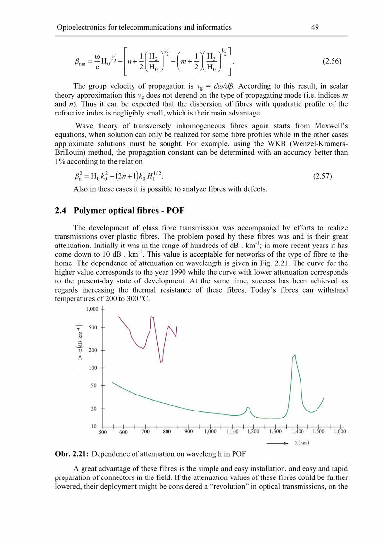
Optoelectronics for telecommunications and informatics 49
.H
H
2
1
H
H
2
1H
c
21
0
32
1
0
221
0nm
mnβ (2.56)
The group velocity of propagation is vg = dω/dβ. According to this result, in scalar theory approximation this vg does not depend on the type of propagating mode (i.e. indices m and n). Thus it can be expected that the dispersion of fibres with quadratic profile of the refractive index is negligibly small, which is their main advantage.
Wave theory of transversely inhomogeneous fibres again starts from Maxwell’s equations, when solution can only be realized for some fibre profiles while in the other cases approximate solutions must be sought. For example, using the WKB (Wenzel-Kramers-Brillouin) method, the propagation constant can be determined with an accuracy better than 1% according to the relation
.12H 2/110
200
2n Hknkβ (2.57)
Also in these cases it is possible to analyze fibres with defects.
2.4 Polymer optical fibres - POF
The development of glass fibre transmission was accompanied by efforts to realize transmissions over plastic fibres. The problem posed by these fibres was and is their great attenuation. Initially it was in the range of hundreds of dB . km-1; in more recent years it has come down to 10 dB . km-1. This value is acceptable for networks of the type of fibre to the home. The dependence of attenuation on wavelength is given in Fig. 2.21. The curve for the higher value corresponds to the year 1990 while the curve with lower attenuation corresponds to the present-day state of development. At the same time, success has been achieved as regards increasing the thermal resistance of these fibres. Today’s fibres can withstand temperatures of 200 to 300 ºC.
Obr. 2.21: Dependence of attenuation on wavelength in POF
A great advantage of these fibres is the simple and easy installation, and easy and rapid preparation of connectors in the field. If the attenuation values of these fibres could be further lowered, their deployment might be considered a “revolution” in optical transmissions, on the

50 FEEC Brno University of Technology
one hand because of the above advantages and, on the other hand, because of the expected radical price reduction.
At this point, fibres of the type of PCS (plastic-core-silicon) should be recalled, which were also used.
As regards the design and transmission, POF is analogous to glass fibre. The core is made of polymethylmethacrylate (PMMA) and the cladding is made of fluorinated PMMA (fluoropolymer).The refraction index of the core is nj = 1.492, that of the cladding is np = 1.416, and NA = 0.47. Schematic diagram and dimensions are given in Fig. 2.22 [2-7].
Currently manufactured fibres have cores of 50, 62.5 and 120 µm in diameter and claddings of 490 µm in diameter. Gigabit Ethernet or multi-gigabit transmissions can be realized to a distance of ca. 200 m, in typical transmission windows of 850 and 1300 nm [2-8].
Obr. 2.22: POF fibre
The transmission problematic is solved by mode theory, and dispersion and other effects, described above, also manifest themselves. Standards issued for POF include IEEE 1394, ATM Forum, etc.
2.5 New technologie sof fibre manufacture
Doped fibres
Chapter 8.16 will deal with optical amplifiers. One of the design possibilities for these amplifiers is the application of the principle of erbium- (or ytterbium-) doped fibre for the wavelength 1.53 – 1.61 µm of laser amplifier (EDFA – Erbium Doped Fibre Amplifier). Use is made of the method of multi-point excitation of active medium in double-cladding (DC) fibres. Excitation is connected to the area of multimode inner cladding of large diameter (not only to the area of single-mode fibre) and thus a power laser diode of large radiation area and low radiant intensity is used for the excitation. The signal itself is then transmitted by the central single-mode doped fibre.
The principle of the method is shown in Fig. 2.23. The principal problem of the method consists in the way the excitation and signal are coupled to the active fibre [2.10], [2.11].
Polarized fibres are designed for special application such as PDM compensators, future coherent transmissions, testing of equipment. They can also be used in metrology, gyroscopes, Doppler speed indicators, and other sensor applications.

Optoelectronics for telecommunications and informatics 51
Single-mode fibres of this type are delivered in yardages or already provided with connectors. A “PANDA” shape section through the fibre with strength members and indicated polarization is shown in Fig. 2.24 [2.11], [2.12]. Axis X is the so-called fast axis, axis Y is the slow axis. The so-called telecommunication polarized fibre, which is specially designed for the polarization multiplexing EDFA excitation laser, is available on the market today.
Obr. 2.23: Principle of excitation into doped fibre, using fused fibre splice element
Obr. 2.24: Polarization
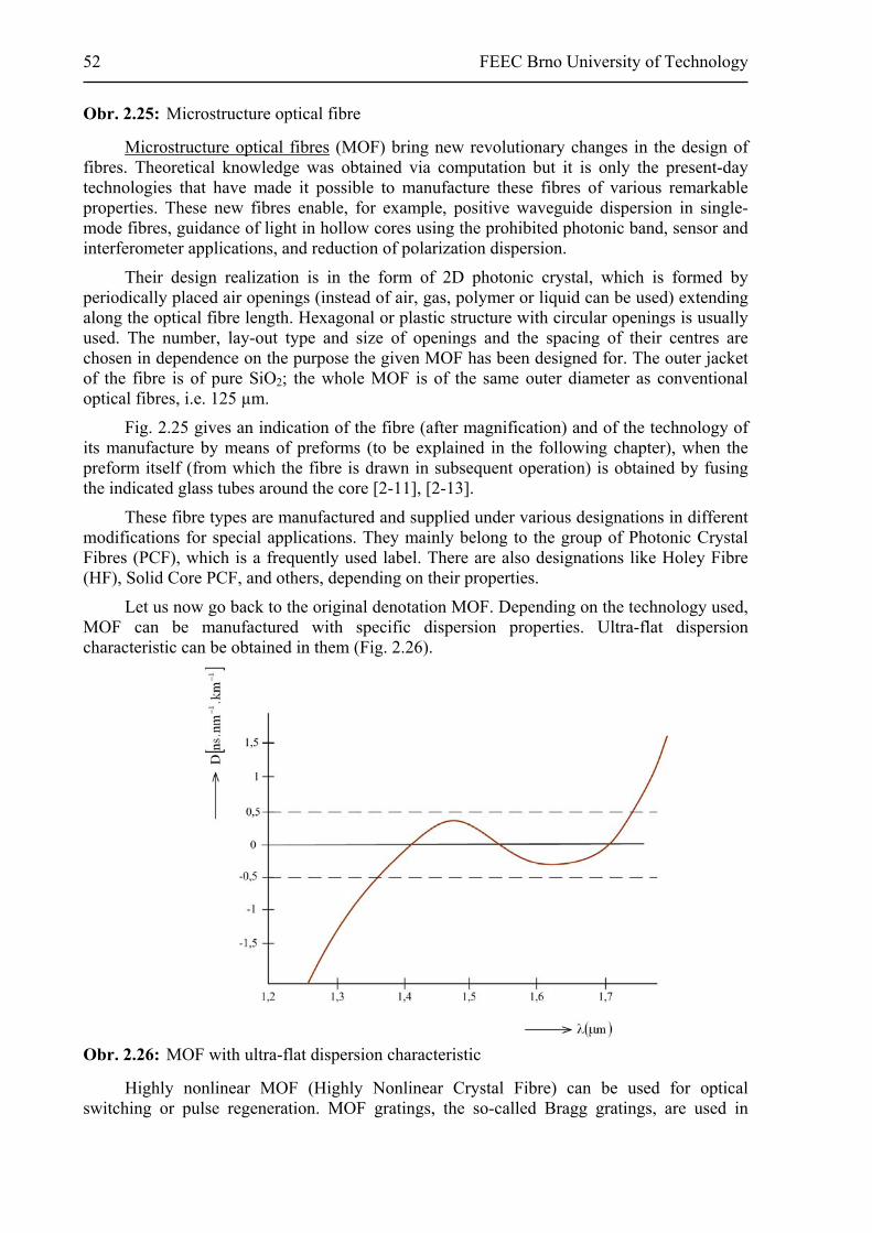
52 FEEC Brno University of Technology
Obr. 2.25: Microstructure optical fibre
Microstructure optical fibres (MOF) bring new revolutionary changes in the design of fibres. Theoretical knowledge was obtained via computation but it is only the present-day technologies that have made it possible to manufacture these fibres of various remarkable properties. These new fibres enable, for example, positive waveguide dispersion in single-mode fibres, guidance of light in hollow cores using the prohibited photonic band, sensor and interferometer applications, and reduction of polarization dispersion.
Their design realization is in the form of 2D photonic crystal, which is formed by periodically placed air openings (instead of air, gas, polymer or liquid can be used) extending along the optical fibre length. Hexagonal or plastic structure with circular openings is usually used. The number, lay-out type and size of openings and the spacing of their centres are chosen in dependence on the purpose the given MOF has been designed for. The outer jacket of the fibre is of pure SiO2; the whole MOF is of the same outer diameter as conventional optical fibres, i.e. 125 µm.
Fig. 2.25 gives an indication of the fibre (after magnification) and of the technology of its manufacture by means of preforms (to be explained in the following chapter), when the preform itself (from which the fibre is drawn in subsequent operation) is obtained by fusing the indicated glass tubes around the core [2-11], [2-13].
These fibre types are manufactured and supplied under various designations in different modifications for special applications. They mainly belong to the group of Photonic Crystal Fibres (PCF), which is a frequently used label. There are also designations like Holey Fibre (HF), Solid Core PCF, and others, depending on their properties.
Let us now go back to the original denotation MOF. Depending on the technology used, MOF can be manufactured with specific dispersion properties. Ultra-flat dispersion characteristic can be obtained in them (Fig. 2.26).
Obr. 2.26: MOF with ultra-flat dispersion characteristic
Highly nonlinear MOF (Highly Nonlinear Crystal Fibre) can be used for optical switching or pulse regeneration. MOF gratings, the so-called Bragg gratings, are used in

Optoelectronics for telecommunications and informatics 53
wavelength multiplexes to lead one channel from the transmitted spectrum; they are suitable for sensor applications, for equalizing the gain in erbium fibre amplifiers, and also for the compensation of dispersion.
Double-core MOF, where light is coupled to one of the cores while from the other core it is coupled to a conventional fibre; power can be seen on the output to flow from one core into the other, with minima and maxima appearing in the transfer function. They are used in fibre filters and sensors.
This problematic is in the stage of research: new structures, manufacturing technologies and methods of fibre splicing are sought, as well as ways of reducing costs since application in the area of transport (long-haul) networks is, for the time being, very costly.
A different situation seems to be emerging in the area of transmissions over short distances, ca. up to 50 m.
POF brings many advantages for this type of transmission. Connecting the fibre to the connector-converter is simple. It suffices to cut the fibre with a knife as need be and “clasp” it down. The systems operate in the region of visible radiation – the state can be checked immediately. In comparison with “glass” optics the costs are very low.
Some companies already offer such products for indoor transmission.
The trend in the development is evidently towards taking the (SI) fibre to the home (FTTH) and realizing further PC, TV and other connections by means of plastic fibres (POF).
Some of these new products can be found in [2-14] and [2-15].
3 Manufacture of optical fibres
In principle, there are two methods for manufacturing optical fibres: either via drawing from a glass preform, whose surface layers are suitably doped with various oxides (so-called gaseous phase – modern manufacturing technology) or as multicomponent fibres (liquid phase method).
The preform is essentially a glass intermediate in the shape of cylindrical rod, from which optical fibre is drawn. The profile of the rod represents an enlarged profile of the optical fibre. After intensive local heating, the fibre is drawn from this preform. It is immediately coated with a layer of polymer of several micrometres in thickness, so-called primary coating, to be mechanically protected. Then it is spooled.
The principle of drawing fibre from a preform is depicted in Fig. 3.1

54 FEEC Brno University of Technology
Obr. 3.1: Drawing optical fibre from preform
This facility is ca. 7 metres tall and relatively quite complicated, provided with precise measurement and control technology using a microcomputer. A feeding mechanism brings the preform into the drawing zone with either a resistance furnace or a burner. On leaving this zone, the fibre is measured immediately below the melting zone and the value measured is sent to the control system. The respective response must not be slower than 0.1 to 0.03 s, and the resultant diameter deviations from the required values must be less than 2 %. Then the coating nozzle applies the primary coating layer to the fibre. In the case of silicone resin a thermal hardening furnace is used while in the case of acrylate UV light is used for hardening. The number of furnaces, or the total length of hardening zone, depends on the rate of drawing. In the deposition of primary coating, rates of up to 5 m . s-1 are achieved. The fibre provided with primary coating is introduced into a drawing machine controlled by the control system. The speed of the drawing machine is controlled on the basis of information about the fibre diameter. The last component of the line is the spooling device, ahead of which a tester of fibre strength is sometimes placed. The fibre-drawing line may contain further devices that simplify the drawing operation or make it more precise [3-1], [3-2].
The preparation of the preform (gaseous phase method) is based on the oxidation of silicon tetrachloride
4 2 2 2SiC O SiO 2C
and other similar oxidation reactions, during which very fine particles of solid oxides are formed. These particles settle on the surface of a suitable carrier and form a porous layer, which due to increased temperature melts into the so-called preform, from which the optical fibre is drawn in the next stage. Different technologies are used in the manufacture of preforms, which differ either in the direction in which the reaction components cross or in the reaction mechanisms. The preparation of the preform is the most important operation in the whole manufacturing process since all the fibre properties are given by the properties of this preform.
In the preparation of the preform by the method of chemical vapour deposition (CVD) the following technologies are used:
Optoelectronics for telecommunications and informatics 55
- OVD (Outside Vapour Deposition), outside deposition from the gaseous phase by way of lateral deposition on the core, which rotates at a constant rate,
- MCVD (Modified Outside Vapour Deposition), which belongs to the inside methods, in which oxides are deposited on the inside wall of rotating silicon tube,
- PCVD (Plasma Chemical Vapour Deposition), in which, the same as with MCVD, oxides are deposited on the inside wall of rotating silicon tube but the reaction according to the starting equations is initiated by microwave plasma,
- VAD (Vapour Phase Axial Deposition), which differs from the preceding technologies in that oxides are deposited in axial direction on a rotating target from the carrier material.
And now some details about the individual technologies.
OVD technology is an original technology of the Corning Glass Works Company (which in 1970 made the first optical fibre with an attenuation of less than 20 dB . km-1) and is used by the Company in the manufacture of optical fibres. This method uses lateral deposition on the core, which rotates at a constant rate. Usually, the core is of 0.5 cm in diameter and made of Al2O3 or graphite. Fuel, SiCl4 and the respective dopants are fed into the burner. The principle of this method is shown in Fig. 3.2. The hydrolysis of halogenide vapours in the flame gives rise to solid soot of oxide or mixture of oxides, part of which settles on the core, forming a porous matter, whose density is about 1/3 of silicon glass density. Doped onto the carrying rod are layers that form in the drawn fibre both the core and the cladding. After doping, the carrier rod is, due to different thermal expansivity, carefully removed and the porous perform will sinter into a clear vitrified preform in the furnace at temperatures around 1500 ºC (Fig. 3.2b). The burning of fuel gas is accompanied by the formation of OH groups. During sintering, the flow of He with a few per cent of Cl2 will remove the OH groups relatively effectively. This method makes heavy demands on the protection against impurities from the surroundings. Controlling the OVD technology is also demanding: it is necessary to maintain constant speeds of the flow of raw materials and fuel, preform revolutions and constant burner temperature. During vitrification the speed of drying gas and perform revolutions and the burner temperature must be constant. During vitrification there are chemical reactions between dopants and drying gas and this leads to changes in the refraction index profile. These changes are corrected in advance, i.e. by such doping that after the reaction with gas the profile is correct. More than 10 km of fibre of 125 μm in diameter can be drawn from a preform. Currently achieved rates of settling are higher than 2 g . min-1, which corresponds to 75 m of fibre per minute. The attenuation values achieved are low, the bandwidth is greater than1 GHz . km-1.
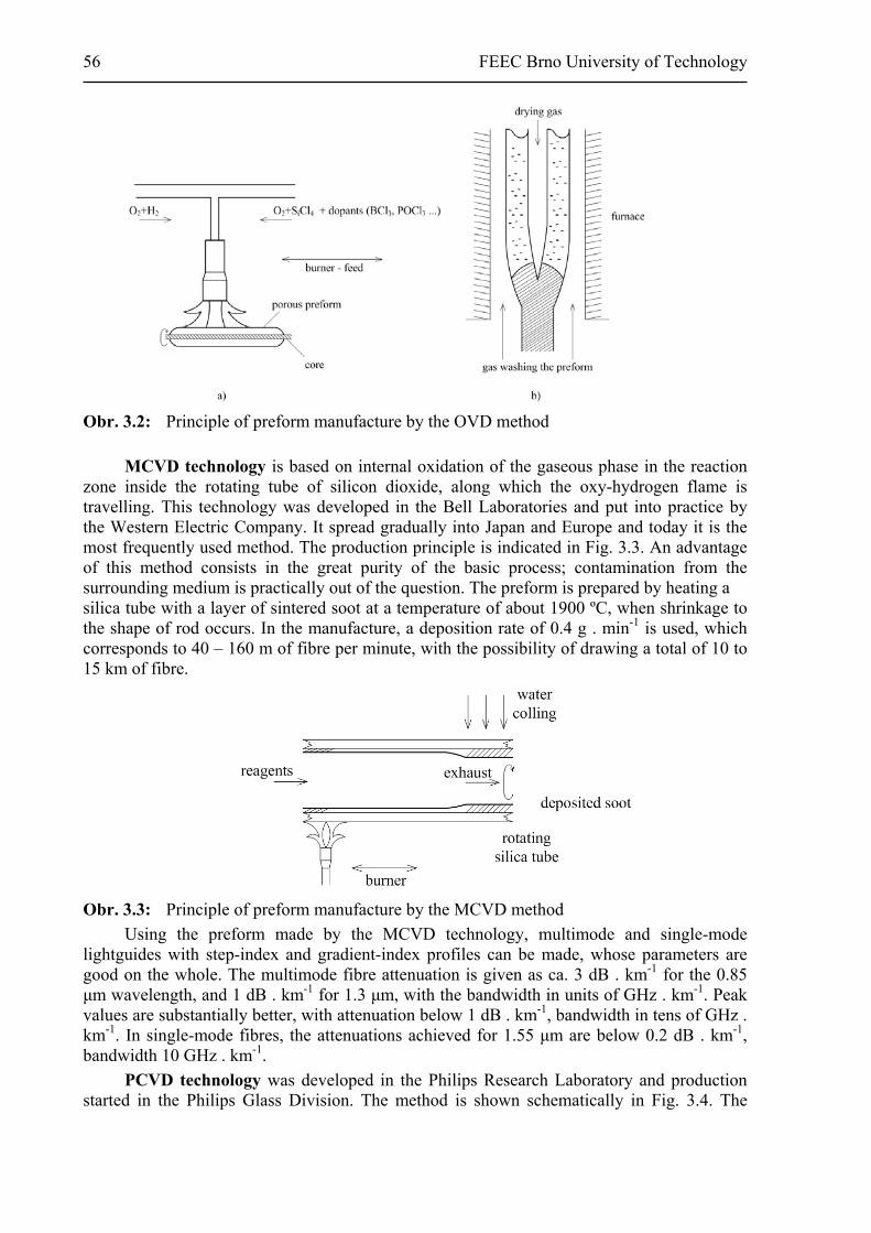
56 FEEC Brno University of Technology
Obr. 3.2: Principle of preform manufacture by the OVD method
MCVD technology is based on internal oxidation of the gaseous phase in the reaction
zone inside the rotating tube of silicon dioxide, along which the oxy-hydrogen flame is travelling. This technology was developed in the Bell Laboratories and put into practice by the Western Electric Company. It spread gradually into Japan and Europe and today it is the most frequently used method. The production principle is indicated in Fig. 3.3. An advantage of this method consists in the great purity of the basic process; contamination from the surrounding medium is practically out of the question. The preform is prepared by heating a silica tube with a layer of sintered soot at a temperature of about 1900 ºC, when shrinkage to the shape of rod occurs. In the manufacture, a deposition rate of 0.4 g . min-1 is used, which corresponds to 40 – 160 m of fibre per minute, with the possibility of drawing a total of 10 to 15 km of fibre.
Obr. 3.3: Principle of preform manufacture by the MCVD method
Using the preform made by the MCVD technology, multimode and single-mode lightguides with step-index and gradient-index profiles can be made, whose parameters are good on the whole. The multimode fibre attenuation is given as ca. 3 dB . km-1 for the 0.85 μm wavelength, and 1 dB . km-1 for 1.3 μm, with the bandwidth in units of GHz . km-1. Peak values are substantially better, with attenuation below 1 dB . km-1, bandwidth in tens of GHz . km-1. In single-mode fibres, the attenuations achieved for 1.55 μm are below 0.2 dB . km-1, bandwidth 10 GHz . km-1.
PCVD technology was developed in the Philips Research Laboratory and production started in the Philips Glass Division. The method is shown schematically in Fig. 3.4. The

Optoelectronics for telecommunications and informatics 57
method is also ranked among the inside methods and is characterized by the application of non-isothermal plasma, in which the reaction proper takes place. A pressure of 1330 Pa is maintained in the tube, which is placed horizontally in the furnace at a temperature of 1200 ºC. Inside the furnace, a microwave generator is moving around the tube at a rate of 8 m . min-1 along a length of 70 cm, operating with 2.45 GHz frequency. This generator generates microwave plasma, in which a heterogeneous reaction is taking place on the tube walls, with no soot being produced. For SiO2 the deposition efficacy is almost 100 % while for GeO2 it is ca. 85 %. The method described yields very thin layers (up to 700 layers of about 0.5 μm), which is of advantage for fibres with gradient-index profile in particular. This is due to the fact that energy for the reaction is supplied directly and not through tube walls. After the deposition of the core materials the furnace temperature is raised to 2000 ºC followed by the collapse of silica tube. The manufacturing rate of deposition is 0.5 g . m-1.
Obr. 3.4: Preform manufacture by the PCVD technology
The control of PCVD is easier than that of the other methods. Heavy demands are made on the amount of raw materials; the other parameters such as pressure in the tube, furnace temperature, plasma energy, resonator speed, etc. do not affect the resultant parameters substantially. The collapse is the same as with the MCVD method.
VAD technology was developed in Japan by the NTT Company, and production was started in Fujikura Cable Works Ltd., Sumitomo Electric Industries Ltd, and in other companies. The basic schematic diagram of this method is given in Fig. 3.5. With this method, the particles, which later form the core and the cladding, are deposited on a substrate in axial direction and thus a cylinder without central opening is formed. Important is not only the absence of any central opening, which leads to a reduction of losses, but mainly the possibility of continual preparation of the preform. Vitrification takes place in an electric furnace at 1500 ºC in a He-CO2 or He-SiCl2 atmosphere, in which water is repulsed. In the course of vitrification the preform volume is reduced eight times and the preform diameter is ca. 2.5 cm. It is then elongated to a diameter of 1 cm and placed in the silica tube, and the tube collapses. With this technology, no central dip appears in the refractive index profile. A typical deposition value is 0.4 g . min-1 and the preform can yield over 100 km of fibre. Using this method, both multimode and single-mode step-index and gradient-index lightguides can be prepared, with very low attenuation (below 1 dB . km-1) and large bandwidth. The tensile strength of the fibre is also good.

58 FEEC Brno University of Technology
Obr. 3.5: Preform manufacture by the VAD technology
Controlling the VAD process is very demanding. The refractive index profile is affected by the temperature distribution on the preform surface, flame position and angle. The flow rate of raw materials, fuel and exhaust, the rotation rate of porous preform, and the position of the growing end must be constant. Increasing the deposition rate entails problems. Efficacy of SiO2 deposition is 60 to 80%. In the manufacture of single-mode fibres one burner is used for the deposition of core and one or more burners for the deposition of cladding.
Liquid phase methods. In these methods the so-called multi-component fibres are based on classical glass-making methods. These methods were used when the manufacture of optical fibres was launched. The basic manufacturing operations are the preparation and melting of initial bulk glass and the drawing of fibre.
The first phase consists in preparing ultra-pure starting materials, mostly powder oxides and carbonates. These materials are prepared by using diverse purification methods and by combining them. One of the methods for obtaining silicon dioxide of required purity is to refine the natural raw material via washing in acid solutions, in particular concentrated hydrofluoric acid and nitric acid in 1:1 ratio, and also hydrochloric acid. Synthetic SiO2 powder is prepared by hydrolysis of tetraethoxysilane or silicon tetrachloride; it can be purified via repeated distillation and subsequent drying in dry gas atmosphere. Sodium carbonate is comparatively easy to purify by filtering a 25% solution on filter paper, chip filtration on cellulose acetate membrane and also by electrolysis with mercury cathode.
The second phase is melting, when homogeneous glass without bubbles is obtained; difficulties may arise due to the danger of glass being contaminated with crucible material and furnace medium. Crucibles made of aluminium oxide and platinum are responsible for contamination with iron; the solution is to use raw materials with low melting temperature and, consequently, crucibles of pure silica can be used. But then the crucible material starts dissolving and striae appear. This can be prevented by high-frequency heating of bulk glass and simultaneous cooling of crucible. Drying gases are made to bubble through the bulk glass in order to reduce the content of hydroxyl ions. After cooling, the glass is machined to the required dimensions or it is allowed to cool only partially and a rod is drawn from its surface;

Optoelectronics for telecommunications and informatics 59
this will eliminate contamination stemming from machining but at the cost of lower glass homogeneity.
For the fibre-drawing itself, two basic methods are used: the method of “rod in the tube” and the method of “double crucible”.
Obr. 3.6: The “rod in the tube” method of manufacturing optical fibre
The “rod in the tube” method is particularly simple and productive. A rod of extremely pure glass or fused silica is inserted into a tube of glass of low refractive index and subsequent heating allows a fibre to be drawn (see Fig. 3.6). A disadvantage is that geometrical and structural imperfections of the inner surface of the rod can show as defects of the core-cladding interface, which cause diffusion losses. The method is used for the preparation of cheap multimode step-index lightguides, comparatively large attenuation and great numerical aperture. The lowest attenuation of the lightguides is ca. 6 dB . km-1 and the numerical aperture is 0.6. The prepared initial material of 25 mm in diameter and 500 mm in length can yield about 20 km of fibre.
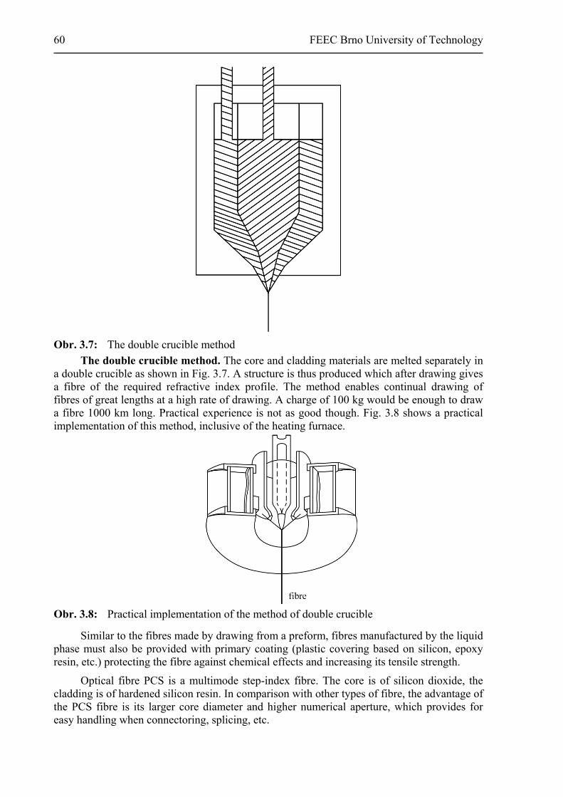
60 FEEC Brno University of Technology
Obr. 3.7: The double crucible method
The double crucible method. The core and cladding materials are melted separately in a double crucible as shown in Fig. 3.7. A structure is thus produced which after drawing gives a fibre of the required refractive index profile. The method enables continual drawing of fibres of great lengths at a high rate of drawing. A charge of 100 kg would be enough to draw a fibre 1000 km long. Practical experience is not as good though. Fig. 3.8 shows a practical implementation of this method, inclusive of the heating furnace.
Obr. 3.8: Practical implementation of the method of double crucible
Similar to the fibres made by drawing from a preform, fibres manufactured by the liquid phase must also be provided with primary coating (plastic covering based on silicon, epoxy resin, etc.) protecting the fibre against chemical effects and increasing its tensile strength.
Optical fibre PCS is a multimode step-index fibre. The core is of silicon dioxide, the cladding is of hardened silicon resin. In comparison with other types of fibre, the advantage of the PCS fibre is its larger core diameter and higher numerical aperture, which provides for easy handling when connectoring, splicing, etc.
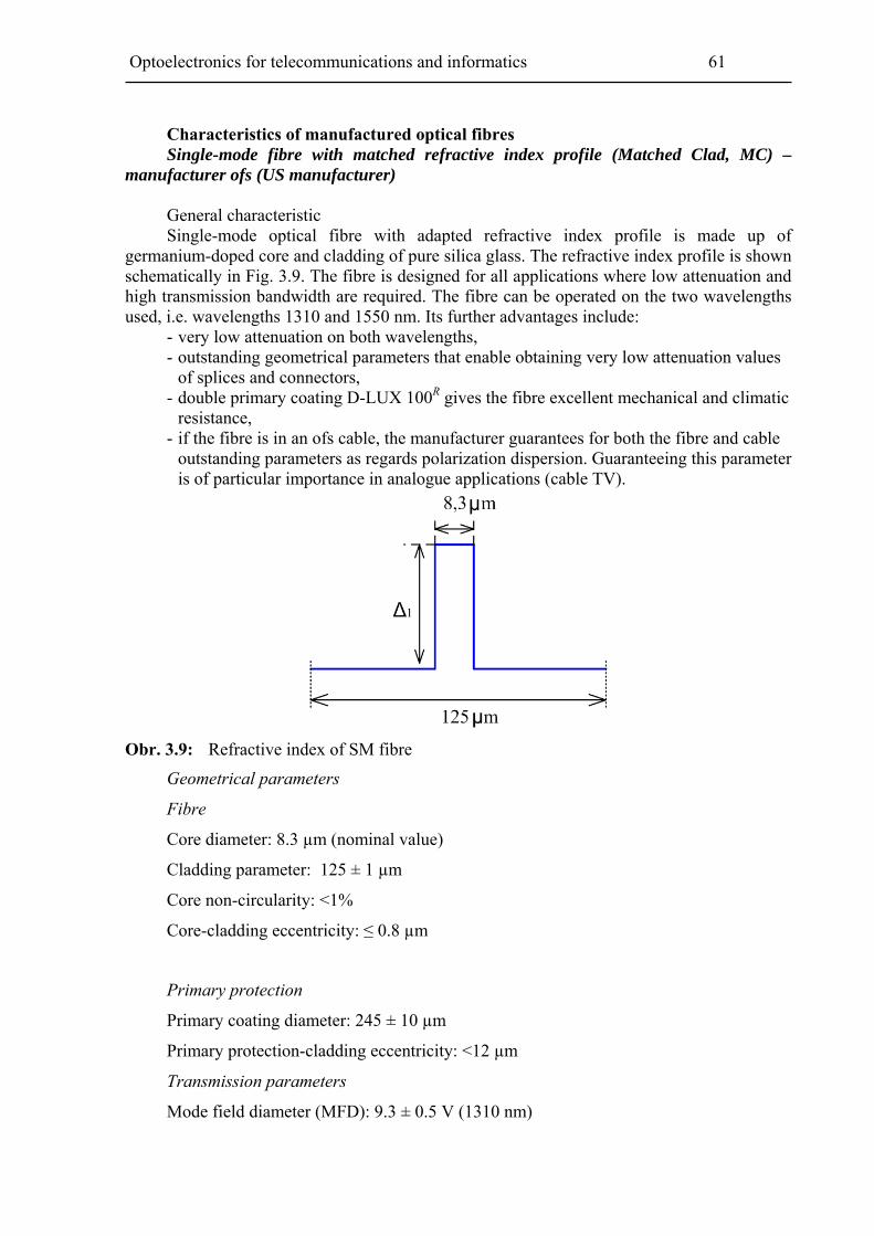
Optoelectronics for telecommunications and informatics 61
Characteristics of manufactured optical fibres Single-mode fibre with matched refractive index profile (Matched Clad, MC) –
manufacturer ofs (US manufacturer)
General characteristic Single-mode optical fibre with adapted refractive index profile is made up of germanium-doped core and cladding of pure silica glass. The refractive index profile is shown schematically in Fig. 3.9. The fibre is designed for all applications where low attenuation and high transmission bandwidth are required. The fibre can be operated on the two wavelengths used, i.e. wavelengths 1310 and 1550 nm. Its further advantages include:
- very low attenuation on both wavelengths, - outstanding geometrical parameters that enable obtaining very low attenuation values
of splices and connectors, - double primary coating D-LUX 100R gives the fibre excellent mechanical and climatic
resistance, - if the fibre is in an ofs cable, the manufacturer guarantees for both the fibre and cable
outstanding parameters as regards polarization dispersion. Guaranteeing this parameter is of particular importance in analogue applications (cable TV).
Obr. 3.9: Refractive index of SM fibre
Geometrical parameters
Fibre
Core diameter: 8.3 µm (nominal value)
Cladding parameter: 125 ± 1 µm
Core non-circularity: <1%
Core-cladding eccentricity: ≤ 0.8 µm
Primary protection
Primary coating diameter: 245 ± 10 µm
Primary protection-cladding eccentricity: <12 µm
Transmission parameters
Mode field diameter (MFD): 9.3 ± 0.5 V (1310 nm)

62 FEEC Brno University of Technology
10.5 ± 1.0 µm (1550 nm)
Cut-off wavelength (λcut off): 1150 – 1350 nm (for 2 m fibre length)
Cut-off wavelength in cable: ≤ 1260 nm
Attenuation (customer specifies maximum value from the range): 0.35 0.40 dB . km-1 per
nm, 0.21 – 0.30 dB . km-1 per 1550 nm
Spectral change in attenuation: ≤ 0.1 dB . km-1 in the interval 1285-1330 nm
≤ 0.05 dB . km-1 in the interval 1525-1575 nm
Longitudinal homogeneity of attenuation: no point discontinuities > 0.1 dB
Attenuation on wavelength of absorption maximum of OH-ions (1383 ± 3 µm) ≤ 2 dB .
km-1
Chromatic dispersion
Wavelength of zero chromatic dispersion λ0: 1300-1322 nm (typically 1312 nm)
Dispersion between 1200 and 1600 nm can be calculated according to the relation
D(λ) = 0.25 . S0 . λ . (1-λ/λ0)4
Maximum dispersion on 1550 nm: 18 ps/nm-1 . km-1
Maximum slope of dispersion characteristic on the wavelength of zero chromatic
dispersion: S0 ≤ S: 0.092 ps . nm-2 . km-1 (typically 0.088 ps . nm-2 . km-1)
Losses due to macrobends:
Less than 0.5 dB on one turn of 32 mm in diameter on λ = 1550 nm.
Less than 0.05 dB on 1310 nm and less than 0.1 dB on 1550 nm on 100 turns of 75 mm in
diameter
Polarization mode dispersion: 0.5 ps/ √km on 1310 nm (in ofs cable).
Mechanical parameters
Tensile strength (Proof Test): 0.7 GPa
Stripping force of primary coating: <8.9 N, ≥ 1.3 N
Climatic resistance
Temperature dependence of attenuation: ≤ 0.05 dB . km-1 within the range -60 °C to
+85°C.
Static fatigue: static value coefficient is > 20 if D-LUX 100R protection is used.
Endurance of colour marking:
Colour-marked fibres in the D-LUX 100R primary coating do not exhibit any changes in
colour after the following aging tests:
- 30 days at 95 °C and 95% relative air humidity
- 20 days in dry heat of 125 °C

Optoelectronics for telecommunications and informatics 63
The other characteristics
Relative refractive index difference: Δ1 = 0.33%
Effective group refractive index: 1310 nm 1.466
1550 nm 1.467
Numerical aperture: 0.12
Rayleigh’s back-scattering coefficient: 1310 nm -49.6 dB
1550 nm -52.1 dB
Fibre curl: curl radius ≥ 2 m
Single-mode fibre with depressed refractive index profile (Depressed Clad, DC)
General characteristic
Single-mode optical fibre with depressed refractive index profile is made up of germanium-doped core, inner cladding with reduced refractive index profile, and outer cladding of pure silica glass. The refractive index profile is shown schematically in Fig. 3.10. The fibre is designed for all applications where low attenuation and high transmission bandwidth are required. The fibre can be operated on the two wavelengths used, i.e. wavelengths 1310 and 1550 nm. Its further advantages include:
- very low attenuation on both wavelengths, - outstanding geometrical parameters that enable obtaining very low attenuation values
of splices and connectors, - the depressed refractive index profile provides excellent resistance of attenuation to
microbends and macrobends, even in the case of changing to the 1550 nm wavelength, - double primary coating D-LUX 100R gives the fibre excellent mechanical and climatic
resistance, - if the fibre is in an ofs cable, the manufacturer guarantees for both the fibre and the
cable outstanding parameters as regards polarization dispersion. Guaranteeing this parameter is of particular importance in analogue applications (cable TV).
Obr. 3.10: Refractive index profile
Geometrical parameters Fibre
Core diameter: 8.3 µm (nominal value) Cladding parameter: 125 ± 1 µm
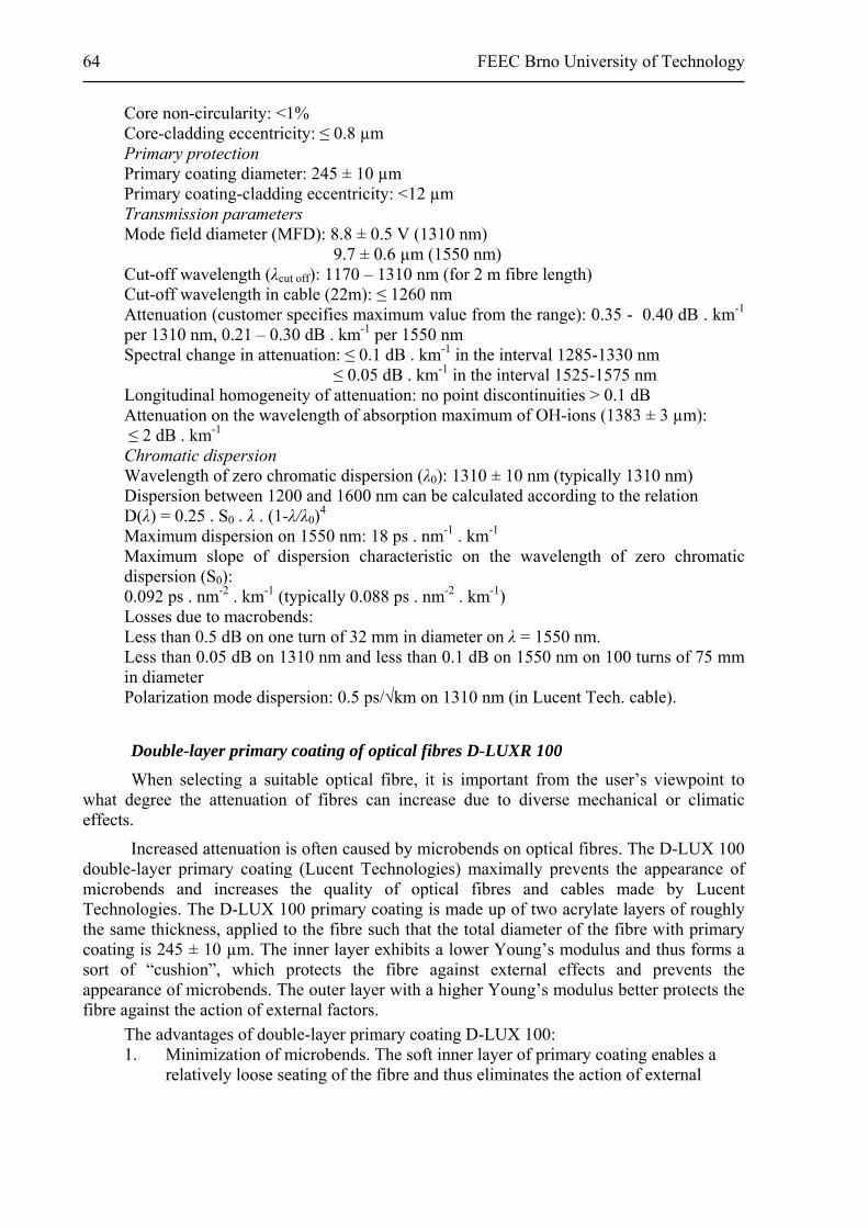
64 FEEC Brno University of Technology
Core non-circularity: <1% Core-cladding eccentricity: ≤ 0.8 µm Primary protection Primary coating diameter: 245 ± 10 µm Primary coating-cladding eccentricity: <12 µm Transmission parameters Mode field diameter (MFD): 8.8 ± 0.5 V (1310 nm) 9.7 ± 0.6 µm (1550 nm) Cut-off wavelength (λcut off): 1170 – 1310 nm (for 2 m fibre length) Cut-off wavelength in cable (22m): ≤ 1260 nm Attenuation (customer specifies maximum value from the range): 0.35 - 0.40 dB . km-1 per 1310 nm, 0.21 – 0.30 dB . km-1 per 1550 nm Spectral change in attenuation: ≤ 0.1 dB . km-1 in the interval 1285-1330 nm ≤ 0.05 dB . km-1 in the interval 1525-1575 nm Longitudinal homogeneity of attenuation: no point discontinuities > 0.1 dB Attenuation on the wavelength of absorption maximum of OH-ions (1383 ± 3 µm): ≤ 2 dB . km-1 Chromatic dispersion Wavelength of zero chromatic dispersion (λ0): 1310 ± 10 nm (typically 1310 nm) Dispersion between 1200 and 1600 nm can be calculated according to the relation D(λ) = 0.25 . S0 . λ . (1-λ/λ0)
4 Maximum dispersion on 1550 nm: 18 ps . nm-1 . km-1 Maximum slope of dispersion characteristic on the wavelength of zero chromatic dispersion (S0): 0.092 ps . nm-2 . km-1 (typically 0.088 ps . nm-2 . km-1) Losses due to macrobends: Less than 0.5 dB on one turn of 32 mm in diameter on λ = 1550 nm. Less than 0.05 dB on 1310 nm and less than 0.1 dB on 1550 nm on 100 turns of 75 mm in diameter Polarization mode dispersion: 0.5 ps/√km on 1310 nm (in Lucent Tech. cable).
Double-layer primary coating of optical fibres D-LUXR 100
When selecting a suitable optical fibre, it is important from the user’s viewpoint to what degree the attenuation of fibres can increase due to diverse mechanical or climatic effects.
Increased attenuation is often caused by microbends on optical fibres. The D-LUX 100 double-layer primary coating (Lucent Technologies) maximally prevents the appearance of microbends and increases the quality of optical fibres and cables made by Lucent Technologies. The D-LUX 100 primary coating is made up of two acrylate layers of roughly the same thickness, applied to the fibre such that the total diameter of the fibre with primary coating is 245 ± 10 µm. The inner layer exhibits a lower Young’s modulus and thus forms a sort of “cushion”, which protects the fibre against external effects and prevents the appearance of microbends. The outer layer with a higher Young’s modulus better protects the fibre against the action of external factors.
The advantages of double-layer primary coating D-LUX 100: 1. Minimization of microbends. The soft inner layer of primary coating enables a
relatively loose seating of the fibre and thus eliminates the action of external

Optoelectronics for telecommunications and informatics 65
forces leading to the appearance of microbends. This property is very important for the fibre behaviour at low temperatures.
2. Increased resistance to effects of external forces. 3. Easy removal of primary coating from the fibre (e.g. for fusing and connectoring). 4. Outstanding stability and long service life of fibres. The D-LUX 100 two-layer primary coating is designed such that it has maximum
resistance to degradation caused by either hydrolysis or oxidation. Fibre with the above primary coating exhibits excellent stability of parameters and long service life in humid and in dry environments. This stability and long service life are responsible for the following advantages:
- colour marking does not change throughout the whole service life of fibre, - the fibres do not get mutually stuck, - for the whole service life of fibres the primary coating does not lose adhesion, and the stripping force necessary for the removal of coating does not markedly change either, - high resistance of fibres to static fatigue.
The D-LUX 100 primary coating is used with all types of ofs fibres.
All Wave Fibre (ofs)
This is a fibre with suppressed OH “peak” between the second and the third windows of the attenuation characteristics of optical fibre. It is denoted ZWP (Zero Water Peak) single-mode fibre, which enables transmission in the waveband of 1260 – 1625 nm. The fibre is suitable for CWDM and DWDM transmissions as well as for access networks (FTTx), etc.
It also exhibits very low PDM values. The fibre is manufactured in compliance with the ITU-T G.652D standard.
Geometrical parameters Fibre Core diameter: 8.3 μm Cladding diameter: 125 ± 0.7 μm Core-cladding eccentricity: ≤ 0.5 μm Primary coating diameter: 235 – 245 μm
Transmission parameters Attenuation 1310 nm ≤ 0.34 dB . km-1
1385 nm ≤ 0.31 dB . km-1 1490 nm ≤ 0.24 dB . km-1
1550 nm ≤ 0.21 dB . km-1 1625 nm ≤ 0.24 dB . km-1
Chromatic dispersion: S0 ≤ S: 0.09 ps . nm-2 . km-1 (typically 0.087 ps . nm-2 . km-1) Polarization mode dispersion: < 0.06 ps √km Temperature range: -60 ºC - +85 ºC
All Wave FLEX Fibre (ofs)
It is designed for the installation of FTTH (or FTTx) networks. Its specification corresponds to that of the preceding fibre but exhibits greater reliability and very low transmission losses. It complies with the ITU-T G.657 recommendations.
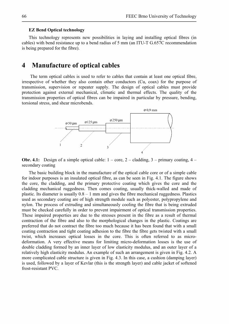
66 FEEC Brno University of Technology
EZ Bend Optical technology
This technology represents new possibilities in laying and installing optical fibres (in cables) with bend resistance up to a bend radius of 5 mm (an ITU-T G.657C recommendation is being prepared for the fibre).
4 Manufacture of optical cables
The term optical cables is used to refer to cables that contain at least one optical fibre, irrespective of whether they also contain other conductors (Cu, coax) for the purpose of transmission, supervision or repeater supply. The design of optical cables must provide protection against external mechanical, climatic and thermal effects. The quality of the transmission properties of optical fibres can be impaired in particular by pressure, bending, torsional stress, and shear microbends.
Obr. 4.1: Design of a simple optical cable: 1 – core, 2 – cladding, 3 – primary coating, 4 – secondary coating
The basic building block in the manufacture of the optical cable core or of a simple cable for indoor purposes is an insulated optical fibre, as can be seen in Fig. 4.1. The figure shows the core, the cladding, and the primary protective coating which gives the core and the cladding mechanical ruggedness. Then comes coating, usually thick-walled and made of plastic. Its diameter is usually 0.8 – 1 mm and gives the fibre mechanical ruggedness. Plastics used as secondary coating are of high strength module such as polyester, polypropylene and nylon. The process of extruding and simultaneously cooling the fibre that is being extruded must be checked carefully in order to prevent impairment of optical transmission properties. These impaired properties are due to the stresses present in the fibre as a result of thermal contraction of the fibre and also to the morphological changes in the plastic. Coatings are preferred that do not contract the fibre too much because it has been found that with a small coating contraction and tight coating adhesion to the fibre the fibre gets twisted with a small twist, which increases optical losses in the core. This is often referred to as micro-deformation. A very effective means for limiting micro-deformation losses is the use of double cladding formed by an inner layer of low elasticity modulus, and an outer layer of a relatively high elasticity modulus. An example of such an arrangement is given in Fig. 4.2. A more complicated cable structure is given in Fig. 4.3. In this case, a cushion (damping layer) is used, followed by a layer of Kevlar (this is the strength layer) and cable jacket of softened frost-resistant PVC.

Optoelectronics for telecommunications and informatics 67
Obr. 4.2: Optical cable: 1 – optical fibre, 2 – outer plastic cladding, 3 – PVC jacket
Obr. 4.3: Single-fibre optical cable: 1 – optical fibre, 2 – cushion, 3 – Kevlar, 4 – PVC
Optical cables are manufactured in runs of 1 000 m, 2 000 m, up to a maximum length of 10 000 m.
Another example of a light single-mode optical cable is given in Fig. 4.4. The optical fibre is in the centre of cable core, surrounded by strength members of Kevlar and then a plastic jacket.
Obr. 4.4: Single-fibre optical cable: 1 – optical fibre, 2 – Kevlar reinforcement, 3 – plastic jacket

68 FEEC Brno University of Technology
Fig. 4.5 shows schematically a single-fibre optical cable combined with Cu pairs.
Obr. 4.5: Schematic illustration of combined single-fibre optical cable with Cu pairs added
A more complicated multi-fibre version is shown in Fig. 4.6. It is based on the classical structure where the strength member (Kevlar) is in the centre of cable core while the next layer contains the respective variable number of optical fibres (inclusive of loose cavities since the design is the same for different numbers of fibres because optical fibres make up a considerable part of the price of cable), and then comes the PVC jacket.
Obr. 4.6: Six-fibre optical cable: 1 – 19 strength members of Kevlar, 2 – optical fibres, 3 – filler, 4 – jacket
A similar design variant is shown in Fig. 4.7.
Obr. 4.7: Two-fibre optical cable: 1 – strength member, 2 – optical fibres, 3 – filler, 4 – cushion, 5 – PVC jacket
Another possible variant has the fibres in the centre of cable core while the cladding and possibly strength members are in the next layers (see Figs 4.8 and 4.9).
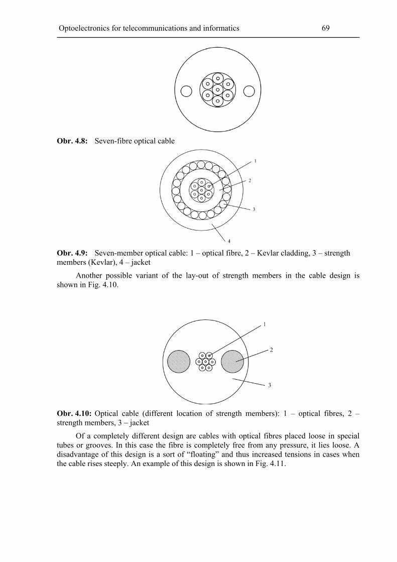
Optoelectronics for telecommunications and informatics 69
Obr. 4.8: Seven-fibre optical cable
Obr. 4.9: Seven-member optical cable: 1 – optical fibre, 2 – Kevlar cladding, 3 – strength members (Kevlar), 4 – jacket
Another possible variant of the lay-out of strength members in the cable design is shown in Fig. 4.10.
Obr. 4.10: Optical cable (different location of strength members): 1 – optical fibres, 2 – strength members, 3 – jacket
Of a completely different design are cables with optical fibres placed loose in special tubes or grooves. In this case the fibre is completely free from any pressure, it lies loose. A disadvantage of this design is a sort of “floating” and thus increased tensions in cases when the cable rises steeply. An example of this design is shown in Fig. 4.11.

70 FEEC Brno University of Technology
Obr. 4.11: Optical cable with loosely placed fibres: 1 – strength member, 2 – cushion, 3 – plastic tube, 4 – optical fibre, 5 - plastic coatings, 6 – jacket
This design group also covers the so-called slotted cables, where one or more fibres can lie loosely in individual cavities (see Fig. 4.12) and cables with the so-called cellular structure, where a great number of fibres can be placed clearly arranged (see Fig. 4.13).
Obr. 4.12: Slotted optical cable: 1 – strength member, 2 – profiling, 3 – fibre, 4 – jacket
Obr. 4.13: Optical cable with cellular structure: 1 – optical fibres, 2 – cells, 3 – plastic filler, 4 - jacket
The profiles of slots and cells can be different. Loose placement thus assures the least possible mechanical loading of fibres and thus a minimum added attenuation and long service life, and the properties of optical fibres are in no way changed by cabling. The disadvantages are that in the case of vertical placement of cable the fixed position is not preserved, and that in the case of freezing over the fibres get bent and thus losses increase, possibly damaging the whole cable [3-1].
Another possible variant is the ribbon cable. First, ribbons with fibres placed next to each other are made. These ribbons are then joined into a matrix, which is twisted and thus enables the cable to withstand bends of usual radii. Fig. 4.14 shows one such design variant with a 6 x 3 matrix (in real execution the number of fibres in the matrix is usually greater, e.g. 12 x 12 = 144 fibres). The main advantage of this design is the quick connectoring of cable
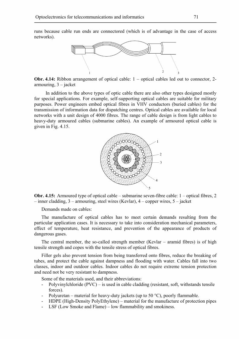
Optoelectronics for telecommunications and informatics 71
runs because cable run ends are connectored (which is of advantage in the case of access networks).
Obr. 4.14: Ribbon arrangement of optical cable: 1 – optical cables led out to connector, 2- armouring, 3 – jacket
In addition to the above types of optic cable there are also other types designed mostly for special applications. For example, self-supporting optical cables are suitable for military purposes. Power engineers embed optical fibres in VHV conductors (buried cables) for the transmission of information data for dispatching centres. Optical cables are available for local networks with a unit design of 4000 fibres. The range of cable design is from light cables to heavy-duty armoured cables (submarine cables). An example of armoured optical cable is given in Fig. 4.15.
Obr. 4.15: Armoured type of optical cable – submarine seven-fibre cable: 1 – optical fibres, 2 – inner cladding, 3 – armouring, steel wires (Kevlar), 4 – copper wires, 5 – jacket
Demands made on cables:
The manufacture of optical cables has to meet certain demands resulting from the particular application cases. It is necessary to take into consideration mechanical parameters, effect of temperature, heat resistance, and prevention of the appearance of products of dangerous gases.
The central member, the so-called strength member (Kevlar – aramid fibres) is of high tensile strength and copes with the tensile stress of optical fibres.
Filler gels also prevent tension from being transferred onto fibres, reduce the breaking of tubes, and protect the cable against dampness and flooding with water. Cables fall into two classes, indoor and outdoor cables. Indoor cables do not require extreme tension protection and need not be very resistant to dampness.
Some of the materials used, and their abbreviations: - Polyvinylchloride (PVC) – is used in cable cladding (resistant, soft, withstands tensile
forces). - Polyuretan – material for heavy-duty jackets (up to 50 °C), poorly flammable. - HDPE (High-Density PolyEthylene) – material for the manufacture of protection pipes - LSF (Low Smoke and Flame) – low flammability and smokiness.

72 FEEC Brno University of Technology
- LSF/OH (Low Smoke and Flame Zero Halogen) – low smokiness and flammability without halogens.
- LSHF (Low Smoke Halogen Free) – low smokiness without halogens.
- LSZH (Low Smoke Zero Halogen) – low smokiness without halogens.
There are also special cables manufactured for aggressive chemical environments, cables for very high temperatures (up to 900 °C), cables resistant to radiation, and cables for other unconventional environments.
4.1 Properties of selected type sof optical fibre
The SPCER TYPE 8 cable, manufactured by Sumitomu Electric Industries, is shown in cross-section in Fig. 4.16 (it was the first cable in our country; it connected the ATU Dejvice and ATU Prague Centre exchanges). The strength member is a steel wire of 2.6 mm diameter, insulated with PE insulation. The diameter inclusive of insulation is 5 mm. In four segments there are always 2 optical fibres, i.e. 8 fibres altogether, and between these segments are quads with copper wires of 0.9 mm in diameter, with PE insulation. The core is protected with polystyrene foil of corrugated PE, which is fused to the outer jacket. The total cable diameter is 19 mm. An aluminium foil plays an important role because it hinders the penetration of water vapours, which are very dangerous from the viewpoint of aging and impaired attenuation.
Obr. 4.16: SPCER TYPE 8 cable: 1 – steel strength member, 2 – chamber protection of fibres, 3 – optical fibres, 4 – core coating, 5 – PE cladding, 6 – steel armouring, 7 – anticorrosive compound, 8 – outer jacket.
Technical parameters of the cable: fibre attenuation at 0.85 µm is better than 4 kdB.km-1, at 1.3 µm better than 0.6 dB.km-1, bandwidth 500 MHz, NA 0.2, and the range of operating temperatures from -15 to 60 °C.
This type of cable was used in the first Czechoslovak optic route in Prague in 1984. The cable was laid as follows: a polyethylene tube was pulled into the cable duct and the cable itself (specific weight 380 kg . km-1 was pulled into this tube. This guaranteed a minimum friction coefficient and thus a comparatively low tensile stress in the cable during pulling.
After the installation the whole line was measured; the whole line (twelve fused splices) exhibited an attenuation of 2.5 dB . km-1, which was a far better result than that declared by the manufacturer (manufacturers include an allowance for aging).
Some optical cables are given below:

Optoelectronics for telecommunications and informatics 73
OPTION1 (Lucent Technologies)
Fully dielectric dry optical cable
Application
Optical cable OPTION1 (Outside Plant to Indoor Optical Network) is a fully dielectric universal (outdoor and indoor applications) optical cable with dry inside of the cable core. The design of OPTION1 cable is similar to the design of outdoor cables, providing the required tensile and mechanical properties of this cable for outdoor application. The dry design of cable core enables protecting the cable with a flameproof coating without halogen elements (LSZH – Low Smoke Zero Halogen). The cable is therefore suitable for the outdoor to indoor cable transition, to be used inside buildings.
Obr. 4.17: Cable OPTION1: 1 –optical fibres, 2 – dielectric central member, 3 – protection tube, 4 – water-blocking elements, 5 – rip cord, 6 – aramid yarn, 7 – polyethylene jacket
Cable description
The design of cable OPTION1 (Fig. 4.17) is based on the well-known Loose Tube design. In this design the optical fibres are protected by a tube of loose secondary coating, whose diameter is several times larger than the fibre diameter so that several fibres can be held in the tube. In some cases the tubes are filled with a special gel, which prevents water from penetrating to the fibres and, at the same time, provides relative mechanical independence of the fibre and cable. The protection tubes and fibres are easy to distinguish by the colour marking.
The tubes are wound around the central dielectric strength member. In contrast to the common cables of the Loose Tube type, the core is not filled with gel; protection against water is provided by dry strips impregnated with SAP (Super Absorbent Polymer) material. The absence of gel inside the cable markedly simplifies the preparation of the cable for splicing. The required tensile resistance is provided by the aramid yarn placed under the cable jacket made of an LSZH material. Thanks to this design the OPTION1 cable meets all the requirements put on indoor and outdoor cables. Cable OPTION1 is used with advantage in routes with outdoor-to-indoor transition. Installation costs are greatly reduced because no transition from outdoor cable to indoor cable is necessary ([4-3)].
Properties
- optical cable for outdoor and indoor application, capacity up to 144 fibres, - fully dielectric design,

74 FEEC Brno University of Technology
- LSZH jacket resistant to UV radiation, - inside the cable are absorption strips of SAP material, which prevent water from
spreading along the cable, - for the transition from outdoor to indoor it is not necessary to change the cable, - the ROL reverse oscillation technique used in stranding the tubes during cable
manufacture enables easy access to fibres and simple splicing, - the rip cord makes the removal of individual jacket layers easy, - the cable can be used in the temperature range from -40 to 70 °C, - the cable fulfils all the demands placed on outdoor cables, inclusive of preventing
water penetration, - the dry design of cable core makes installation and maintenance more effective, - the low weight of cable provides for further reduction of installation costs (blowing,
pulling in, transport, etc.), - quality certificates ISO 9001 and Bellcore CSQP have been awarded to the
manufacturer.
Cable designations for the purpose of ordering
AT – S1, S2, SF, S3, S4, S5, S6 – up to 144 fibres
S1 – Operational wavelength 1 = only 1310 nm 2 = the same attenuation on 1310 and 1550 nm 3 = attenuation on 1550 nm is by 0.1 dB/km lower than on 1310 nm 6 = 1550 nm (True Wave TM fibre) R = transmission over 850 and 1300 nm (multimode fibre) S2 – Maximum attenuation on 1310 nm Conventional single-mode fibre B = 035 dB/km 4 = 0.40 dB/km Dispersion shifted fibre (TrueWaveTM fibre) 2 = 0.25 dB/km (1550 nm only) 3 = 0.30 dB/km (1550 nm only) Multimode fibre S = 3.5/1.0 dB/km 160/500 MHz.km (minimum transmission band) U = 3.4/1.0 dB/km (850/1300) 200/500 MHz . km (minimum transmission band) SF – Type of fibre 0 = Lucent DC (Depressed Clad) M = Lucent MC (Matched Clad) D = Lucent DS (Dispersion Shifted SMF) 9 = 62.5/125 µm multimode fibre T = TrueWaveTM fibre S3 – Dielectric central member 1 = D-P S4 – Tensile strength 2 = 2700 N Ss – Solution of fibre protection O = OPTION1 Loose Tube S6 – Number of fibres in one tube 2 = 2 fibres 4 = 4 fibres 6 = 6 fibres
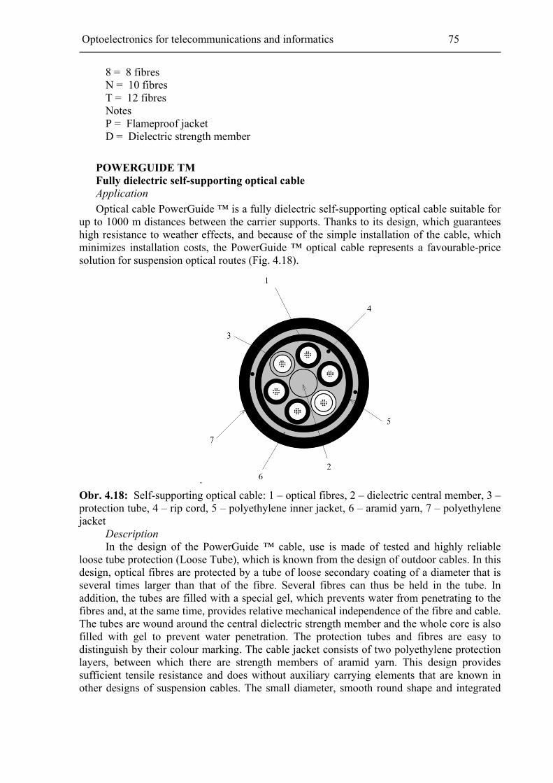
Optoelectronics for telecommunications and informatics 75
8 = 8 fibres N = 10 fibres T = 12 fibres Notes P = Flameproof jacket D = Dielectric strength member
POWERGUIDE TM Fully dielectric self-supporting optical cable Application
Optical cable PowerGuide ™ is a fully dielectric self-supporting optical cable suitable for up to 1000 m distances between the carrier supports. Thanks to its design, which guarantees high resistance to weather effects, and because of the simple installation of the cable, which minimizes installation costs, the PowerGuide ™ optical cable represents a favourable-price solution for suspension optical routes (Fig. 4.18).
.
Obr. 4.18: Self-supporting optical cable: 1 – optical fibres, 2 – dielectric central member, 3 – protection tube, 4 – rip cord, 5 – polyethylene inner jacket, 6 – aramid yarn, 7 – polyethylene jacket Description In the design of the PowerGuide ™ cable, use is made of tested and highly reliable loose tube protection (Loose Tube), which is known from the design of outdoor cables. In this design, optical fibres are protected by a tube of loose secondary coating of a diameter that is several times larger than that of the fibre. Several fibres can thus be held in the tube. In addition, the tubes are filled with a special gel, which prevents water from penetrating to the fibres and, at the same time, provides relative mechanical independence of the fibre and cable. The tubes are wound around the central dielectric strength member and the whole core is also filled with gel to prevent water penetration. The protection tubes and fibres are easy to distinguish by their colour marking. The cable jacket consists of two polyethylene protection layers, between which there are strength members of aramid yarn. This design provides sufficient tensile resistance and does without auxiliary carrying elements that are known in other designs of suspension cables. The small diameter, smooth round shape and integrated
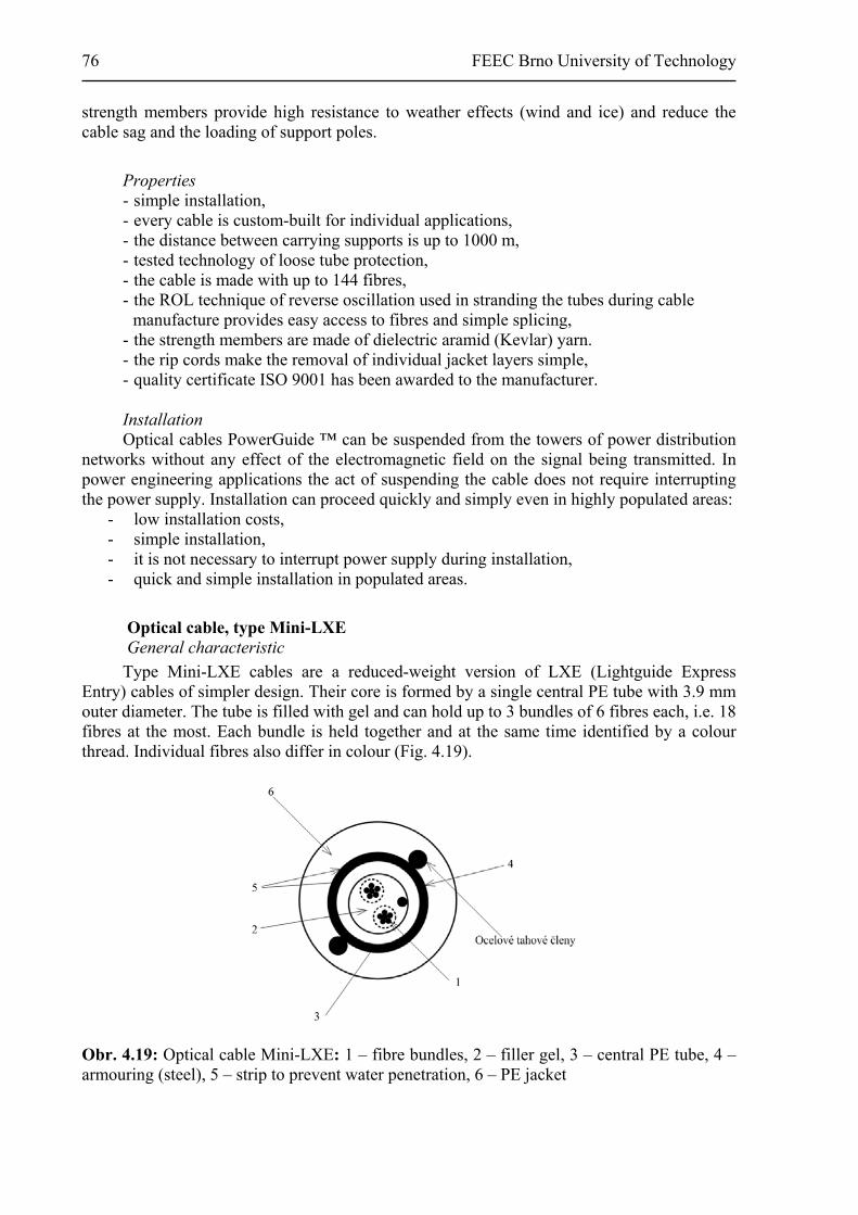
76 FEEC Brno University of Technology
strength members provide high resistance to weather effects (wind and ice) and reduce the cable sag and the loading of support poles.
Properties - simple installation, - every cable is custom-built for individual applications, - the distance between carrying supports is up to 1000 m, - tested technology of loose tube protection, - the cable is made with up to 144 fibres, - the ROL technique of reverse oscillation used in stranding the tubes during cable
manufacture provides easy access to fibres and simple splicing, - the strength members are made of dielectric aramid (Kevlar) yarn. - the rip cords make the removal of individual jacket layers simple, - quality certificate ISO 9001 has been awarded to the manufacturer.
Installation
Optical cables PowerGuide ™ can be suspended from the towers of power distribution networks without any effect of the electromagnetic field on the signal being transmitted. In power engineering applications the act of suspending the cable does not require interrupting the power supply. Installation can proceed quickly and simply even in highly populated areas:
- low installation costs, - simple installation, - it is not necessary to interrupt power supply during installation, - quick and simple installation in populated areas.
Optical cable, type Mini-LXE General characteristic
Type Mini-LXE cables are a reduced-weight version of LXE (Lightguide Express Entry) cables of simpler design. Their core is formed by a single central PE tube with 3.9 mm outer diameter. The tube is filled with gel and can hold up to 3 bundles of 6 fibres each, i.e. 18 fibres at the most. Each bundle is held together and at the same time identified by a colour thread. Individual fibres also differ in colour (Fig. 4.19).
Obr. 4.19: Optical cable Mini-LXE: 1 – fibre bundles, 2 – filler gel, 3 – central PE tube, 4 – armouring (steel), 5 – strip to prevent water penetration, 6 – PE jacket
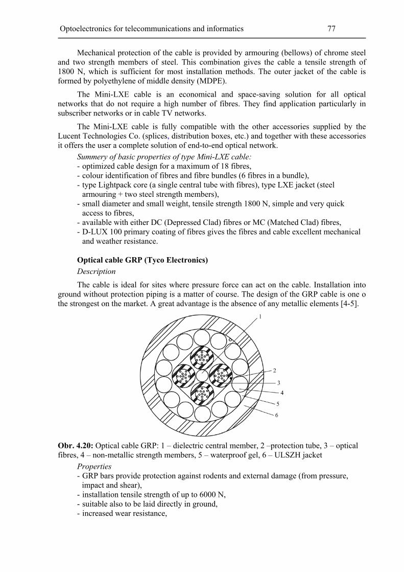
Optoelectronics for telecommunications and informatics 77
Mechanical protection of the cable is provided by armouring (bellows) of chrome steel and two strength members of steel. This combination gives the cable a tensile strength of 1800 N, which is sufficient for most installation methods. The outer jacket of the cable is formed by polyethylene of middle density (MDPE).
The Mini-LXE cable is an economical and space-saving solution for all optical networks that do not require a high number of fibres. They find application particularly in subscriber networks or in cable TV networks.
The Mini-LXE cable is fully compatible with the other accessories supplied by the Lucent Technologies Co. (splices, distribution boxes, etc.) and together with these accessories it offers the user a complete solution of end-to-end optical network.
Summery of basic properties of type Mini-LXE cable: - optimized cable design for a maximum of 18 fibres, - colour identification of fibres and fibre bundles (6 fibres in a bundle), - type Lightpack core (a single central tube with fibres), type LXE jacket (steel
armouring + two steel strength members), - small diameter and small weight, tensile strength 1800 N, simple and very quick
access to fibres, - available with either DC (Depressed Clad) fibres or MC (Matched Clad) fibres, - D-LUX 100 primary coating of fibres gives the fibres and cable excellent mechanical
and weather resistance.
Optical cable GRP (Tyco Electronics)
Description
The cable is ideal for sites where pressure force can act on the cable. Installation into ground without protection piping is a matter of course. The design of the GRP cable is one o the strongest on the market. A great advantage is the absence of any metallic elements [4-5].
Obr. 4.20: Optical cable GRP: 1 – dielectric central member, 2 –protection tube, 3 – optical fibres, 4 – non-metallic strength members, 5 – waterproof gel, 6 – ULSZH jacket
Properties - GRP bars provide protection against rodents and external damage (from pressure,
impact and shear), - installation tensile strength of up to 6000 N, - suitable also to be laid directly in ground, - increased wear resistance,

78 FEEC Brno University of Technology
- without metallic components, - ULSZH or PE jacket, - resistant to water, both longitudinally and transversely, - fibre colours according to TIA/EIA coding for simpler identification, - Temperature range: - single-tube: transport/storage: -20 ºC to +70 ºC, installation: -5 ºC to +50 ºC,
operation: -30 ºC to +70 ºC, - Resistance in shear: - 2000 N for cables with up to 24 fibres, - 4000 N for cables with more than 24 fibres, - 4 to 288 fibres, OM1, OM2, OM3+(OM4), OS1, OS2, ...
Indoor optical cable ACCUMAX
Thanks to its outstanding mechanical properties the ACCUMAX indoor optical cable can be used in practically any indoor applications that do not require a great number of fibres. In telecommunications it can be used, for example, to connect the cable room, where it is usually connected by an optical splice to outdoor cable, and the repeater station, where it can terminate in an optical distribution box or be connected directly to a transmission device. It is particularly suited for FTTD (Fibre to the Desk) applications (Fig. 4.20).
Obr. 4.21: Indoor optical cable
Type ACCUMAX cables contain single-mode optical fibres with double primary coating D-LUX 100 and with tight secondary protection of 0.9 mm outer diameter. The fibres can be either of the DC type (Depressed Clad – depressed refractive index profile) or the MC type (Matched Clad – matched refractive index profile). Fibre identification is provided by coloured tight secondary coating. The maximum number of optical fibres in the ACCUMAX cable is 72. The optical fibres are surrounded by Kevlar fibres, which give the cable its tensile and mechanical strengths. The outer PVC jacket is of yellow colour.
Parameters - Fibre type: Lucent Technologies SM DC or SM MC, - primary coating: D-LUX 100, diameter 245 ± 10 μm, - diameter of tight secondary coating: 0.9 mm, - attenuation (maximum attenuation of fibre in cable): 1310 nm ≤ 0.4 dB/km, 1550 nm ≤ 0.3 dB/km.
- Chromatic dispersion: 1310 nm ≤ 2.8 ps/km . nm. 1550 nm ≤ 18 ps/km . nm, - cut-off wavelength: ≤ 1230 nm, - operational temperature: -20 ºC to +70 ºC.

Optoelectronics for telecommunications and informatics 79
Cable for FTTx networks – Multi Loose Tube Cable As an example, the cable manufactured by the company PRYSMIAN will be given. This is a conventional cable with central strength member. The fibres are held in tubes (MM or SM), the maximum capacity is 720 fibres. In-depth description can be found in [4-7].
Ribbon cable – Fusion Link ™
This cable, with a capacity of up to 216 fibres, is made up of ribbons of 12 fibres each, and is suitable for access networks. The fibres are placed in the centre of the cable core, inserted in a tube and armoured with a steel tube. The strength members are held in the jacket. Cable by the PRYSMIAN Company [4-7].
Self-supporting optical cables A-Dxx
These types of cable with a maximum number of fibres 48 are made with a self-supporting strength member or with the strength member inside the cable core. There are maximally 6 fibres in a tube. The cable has a PE jacket. The maximum spanning distance is 200 m. Ice coating must be taken into consideration. These cables are suitable for the interconnection of buildings. Manufacturer: VUKI Bratislava [4-8].
FIZZER
This is the designation under which the company CDT Optius, Děčín-Podmokly, manufactures and supplies a fireproof cable (without halogen) with fibres (up to 24 of them) placed in a tube in the centre of cable core. The other elements serve as protection and strength members. More details can be found in [4-9].
References in Chapter 4: [4-1], [4-2], [4-3], [4-4], [4-5], [4-6], [4-7], [4-8] and [4-9].
5 Splicing technice, connectors and couplers
The same as metallic cables, optical cables, too, are delivered in (considerably larger) runs, which need to be connected, i.e. individual fibres and then the jacket need to be joined. To join optical fibres is much more complicated than to join metallic cables; jacket splices are in principle identical to splices of plastic cables.
On sites where it will often be necessary to interrupt the optical route, e.g. for the purpose of measuring, optical connectors are used.
Splices in fibre optics can from this viewpoint be divided into: - non-demountable splices, - demountable splices.
Couplers are then used for routing, coupling and separating optical radiation.
5.1 On general problems of splicing
Generally speaking, any connection in optical communication can be regarded as a coupler which, in comparison with metallic conductors, introduces considerable attenuation into the
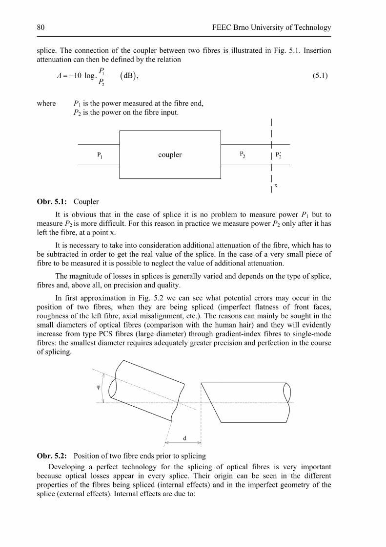
80 FEEC Brno University of Technology
splice. The connection of the coupler between two fibres is illustrated in Fig. 5.1. Insertion attenuation can then be defined by the relation
1
2
10 log. dB ,P
AP
(5.1)
where P1 is the power measured at the fibre end, P2 is the power on the fibre input.
Obr. 5.1: Coupler
It is obvious that in the case of splice it is no problem to measure power P1 but to measure P2 is more difficult. For this reason in practice we measure power P2 only after it has left the fibre, at a point x.
It is necessary to take into consideration additional attenuation of the fibre, which has to be subtracted in order to get the real value of the splice. In the case of a very small piece of fibre to be measured it is possible to neglect the value of additional attenuation.
The magnitude of losses in splices is generally varied and depends on the type of splice, fibres and, above all, on precision and quality.
In first approximation in Fig. 5.2 we can see what potential errors may occur in the position of two fibres, when they are being spliced (imperfect flatness of front faces, roughness of the left fibre, axial misalignment, etc.). The reasons can mainly be sought in the small diameters of optical fibres (comparison with the human hair) and they will evidently increase from type PCS fibres (large diameter) through gradient-index fibres to single-mode fibres: the smallest diameter requires adequately greater precision and perfection in the course of splicing.
Obr. 5.2: Position of two fibre ends prior to splicing
Developing a perfect technology for the splicing of optical fibres is very important because optical losses appear in every splice. Their origin can be seen in the different properties of the fibres being spliced (internal effects) and in the imperfect geometry of the splice (external effects). Internal effects are due to:

Optoelectronics for telecommunications and informatics 81
- changes in the diameters of the core and primary coating of the fibres being spliced, - mismatch of refractive indices, - mismatch of numerical apertures, - ellipticity and non-concentricity of the core and primary coating.
External effects on losses in the splice are the following: - transverse displacement, - longitudinal displacement, - axial misalignment of fibres, - quality of the fibre end preparation, - Fresnel reflections.
External effects can be reduced by first-rate splicing technology. It holds for multimode fibres that the greatest losses are caused by axial refraction and transverse displacement. Longitudinal displacement effects are les pronounced. Fresnel reflection losses at the glass-air-glass interface can be reduced using a suitable filler material whose refractive index is similar to that of the core. The quality of the fibre end is of minimum effect on losses as long as suitable techniques of cleavage and, possibly, grinding and polishing of the front faces of optical fibres are used.
In connection with the above division of splices into those that cannot be demounted and those that can be demounted there are a number of techniques, which will be indicated in the following. The choice of a concrete technique depends on the properties required from the connection.
These properties can be sorted as follows: a) Design solution, which includes:
- multiple or single splice - splice durability, - density of inner lay-out, - installation universality, - magnitude of optical losses, - complexity of the method.
b) Installation properties include: - stability of splice losses, - mechanical robustness, - resistance to environment.
c) Economic factors include: - cost of material per splice, - tools and their cost, - cost of training the installers.
All these important viewpoints need to be taken into consideration. There will be some differences depending on whether multimode or single-mode fibres are concerned.
In the following we will show the dependence of some parameters on potential faulty splices.
Difference in core and fibre diameters
This is the case when two fibres of different diameters are joined and the fibres are axially identical. The dependence of insertion losses is established from relation (5.1)

82 FEEC Brno University of Technology
2
jd
j
10 log ,d
aD
(5.2)
and is graphically illustrated in Fig. 5.3. Substituting into relation (5.2) the maximum deviations of fibre diameters according to the ITU-T recommendation [5-1], d = 2a = 50 μm ± 3 μm, we obtain the deviation ad = 1.05 dB.
Obr. 5.3: Dependence of attenuation on different diameters and NA of optical fibres
Unless specified otherwise, the following formulations of losses hold for multimode fibres.
Difference in NA fibre sizes
In this case the core of the transmitting fibre and the core of the receiving fibre have different numerical apertures NA. Again according to the ITU-T recommendation, for the GI fibre the difference should be NA = 0.2 ± 0.02.
The calculation can be performed according to the relation 2
RNA
T
NA10log .
NAa
(5.3)
The graphical illustration is almost identical to the preceding case and so the result is also obvious from Fig. 5.3.
Transverse displacement of fibre axes
This concerns two fibres that are axially displaced. For the step-index fibre the losses can be expressed according to the relation [5-2]

Optoelectronics for telecommunications and informatics 83
2
12
OS 21
2cosar
2log10
a
e
a
e
a
ea (5.4)
and efficiency according to the relation
o
2 21 .
1
e g
a g
(5.5)
For the gradient-index fibre the losses can be expressed according to the relation 1
2 22
OG
2 110 log ar cos 4 1 2 .
2 2 12
e e e ea
a a a a
(5.6)
Graphical representation of these dependence relations can be seen in Fig. 5.4.
Obr. 5.4: Dependence of attenuation on transverse displacement of fibre axes

84 FEEC Brno University of Technology
Obr. 5.5: Dependence of attenuation on angular misalignment and longitudinal displacement of fibre axes
Angular misalignment
Losses due to the misalignment of opposite fibre axes (acc. to Fig. 5.5) can be expressed for the step-index fibre as
2
1
2
c2
c2
22
1
2
c2
ÚS 1
2sin
sin
sin2
sin1
2sin
sinarctg
2log10a
ΘΘ
(5.7)
and for the gradient-index fibre as 3 1
2 242 2
c cÚG 4
2 22 c
sin sin sin sin2 52 210log ar cos 1 1 .sin sin 3 sin sin
2 2
a
(5.8)
It is obvious from the graphs that for the gradient-index fibres the losses are larger.
Longitudinal displacement of fibres
Longitudinal displacement appears in the connector joining of fibres. Particularly in the case of connector failures this attenuation increases. The dependence is plotted in the graph in Fig. 5.5. The graph shows considerable scatter in the loss values, which have been plotted on the basis of different sources that give practical results of measurements. No theoretical relation has as yet been found for this dependence. Based on measurements, the following term has been determined explicitly for the calculation

Optoelectronics for telecommunications and informatics 85
PS c
410log 1 tg
3a
a
(5.9)
for gradient-index fibres it is necessary to subtract the correction factor
11 .
2K
(5.10)
Losses due to reflection
They appear above all in the case of connectored splices but also in permanent joints on the interface fibre - air (glue, immersion liquid) – fibre. These losses are caused by the Fresnel reflections. The value of these losses is usually not high; it strongly depends on the quality of the surface of fibre ends.
For the calculation a relation can be used that makes use of the well-known reflectance coefficient
2
j 0RS
j 0
10log 1 2 .n n
an n
(5.11)
For a recommended value nj = 1.47 the outcome is aRS = 0.32 dB. The graphical representation of the fibre-air-fibre losses is shown in Fig. 5.6.
Obr. 5.6: Dependence of reflection losses on refractive index of core
For gradient-index fibres the determination of insertion losses is more difficult in view of the varying refractive index. It is possible to introduce the average value of refractive index
2k
0
11 2 ,
ga rn n dr
a a
(5.12)
where the parameter g with regard to the design of gradient-index fibre is equal to 2.
The for the reflection attenuation it holds
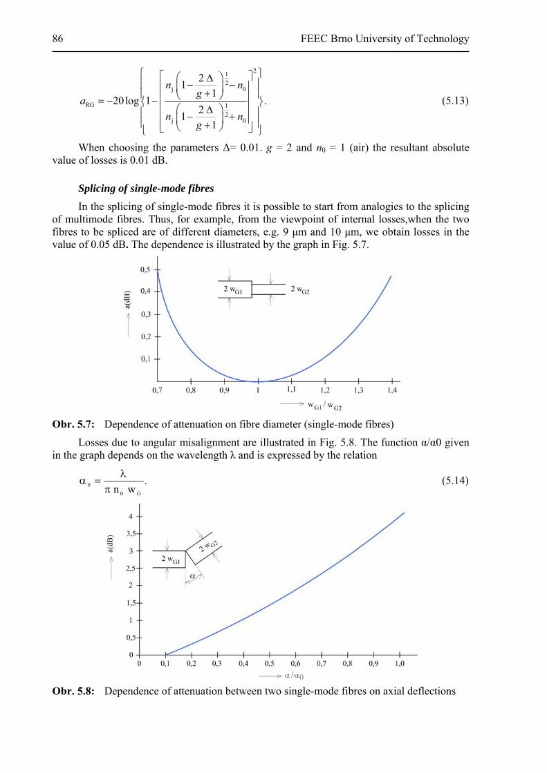
86 FEEC Brno University of Technology
21
2j 0
RG 1
2j 0
21
120log 1 .
21
1
n ng
a
n ng
(5.13)
When choosing the parameters Δ= 0.01. g = 2 and n0 = 1 (air) the resultant absolute value of losses is 0.01 dB.
Splicing of single-mode fibres
In the splicing of single-mode fibres it is possible to start from analogies to the splicing of multimode fibres. Thus, for example, from the viewpoint of internal losses,when the two fibres to be spliced are of different diameters, e.g. 9 μm and 10 μm, we obtain losses in the value of 0.05 dB. The dependence is illustrated by the graph in Fig. 5.7.
Obr. 5.7: Dependence of attenuation on fibre diameter (single-mode fibres)
Losses due to angular misalignment are illustrated in Fig. 5.8. The function α/α0 given in the graph depends on the wavelength λ and is expressed by the relation
.wn G0
0
(5.14)
Obr. 5.8: Dependence of attenuation between two single-mode fibres on axial deflections
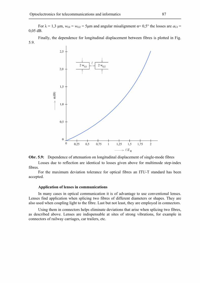
Optoelectronics for telecommunications and informatics 87
For λ = 1,3 μm, wGl = wG2 = 5μm and angular misalignment α= 0,5° the losses are aÚJ = 0,05 dB.
Finally, the dependence for longitudinal displacement between fibres is plotted in Fig. 5.9.
Obr. 5.9: Dependence of attenuation on longitudinal displacement of single-mode fibres
Losses due to reflection are identical to losses given above for multimode step-index fibres. For the maximum deviation tolerance for optical fibres an ITU-T standard has been accepted.
Application of lenses in communications
In many cases in optical communication it is of advantage to use conventional lenses. Lenses find application when splicing two fibres of different diameters or shapes. They are also used when coupling light to the fibre. Last but not least, they are employed in connectors.
Using them in connectors helps eliminate deviations that arise when splicing two fibres, as described above. Lenses are indispensable at sites of strong vibrations, for example in connectors of railway carriages, car trailers, etc.
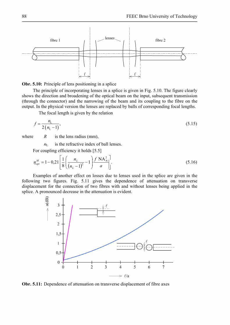
88 FEEC Brno University of Technology
Obr. 5.10: Principle of lens positioning in a splice
The principle of incorporating lenses in a splice is given in Fig. 5.10. The figure clearly shows the direction and broadening of the optical beam on the input, subsequent transmission (through the connector) and the narrowing of the beam and its coupling to the fibre on the output. In the physical version the lenses are replaced by balls of corresponding focal lengths.
The focal length is given by the relation
L
L
,2 1
nf
n
(5.15)
where R is the lens radius (mm),
nL is the refractive index of ball lenses.
For coupling efficiency it holds [5.5]
.
NA1
18
121,01
2N
2
a
f
n
nη
L
LMopt (5.16)
Examples of another effect on losses due to lenses used in the splice are given in the following two figures. Fig. 5.11 gives the dependence of attenuation on transverse displacement for the connection of two fibres with and without lenses being applied in the splice. A pronounced decrease in the attenuation is evident.
Obr. 5.11: Dependence of attenuation on transverse displacement of fibre axes
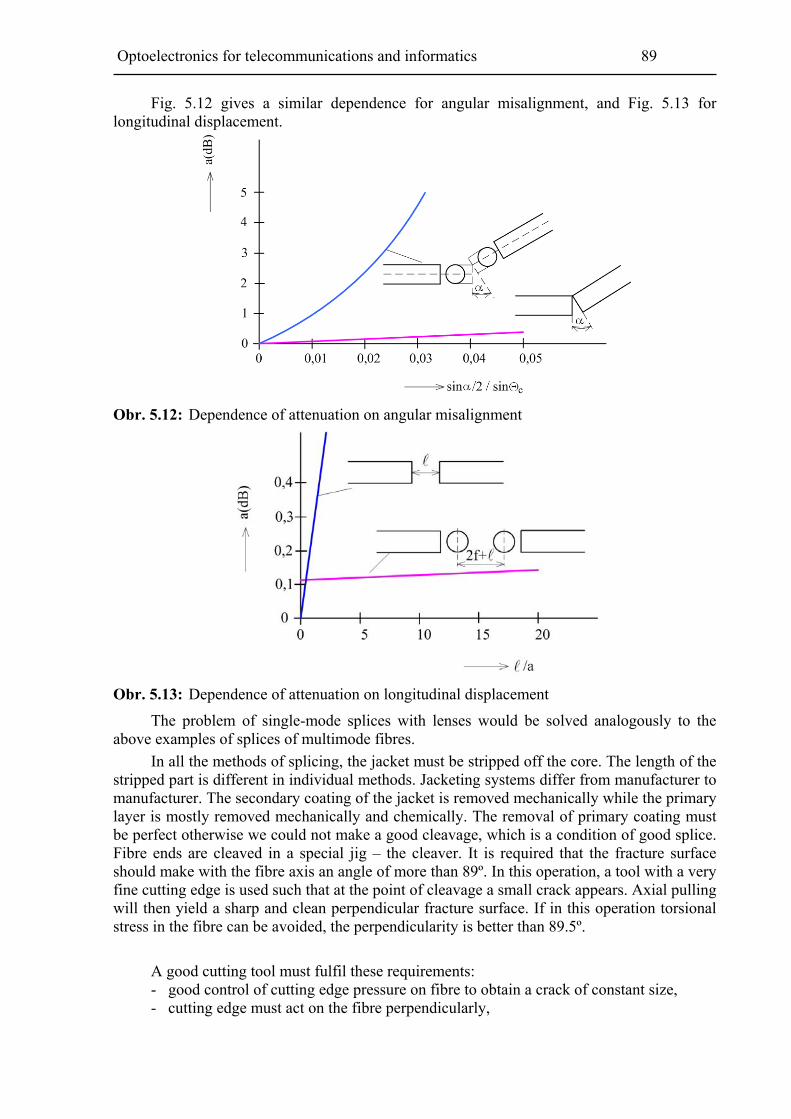
Optoelectronics for telecommunications and informatics 89
Fig. 5.12 gives a similar dependence for angular misalignment, and Fig. 5.13 for longitudinal displacement.
Obr. 5.12: Dependence of attenuation on angular misalignment
Obr. 5.13: Dependence of attenuation on longitudinal displacement
The problem of single-mode splices with lenses would be solved analogously to the above examples of splices of multimode fibres.
In all the methods of splicing, the jacket must be stripped off the core. The length of the stripped part is different in individual methods. Jacketing systems differ from manufacturer to manufacturer. The secondary coating of the jacket is removed mechanically while the primary layer is mostly removed mechanically and chemically. The removal of primary coating must be perfect otherwise we could not make a good cleavage, which is a condition of good splice. Fibre ends are cleaved in a special jig – the cleaver. It is required that the fracture surface should make with the fibre axis an angle of more than 89º. In this operation, a tool with a very fine cutting edge is used such that at the point of cleavage a small crack appears. Axial pulling will then yield a sharp and clean perpendicular fracture surface. If in this operation torsional stress in the fibre can be avoided, the perpendicularity is better than 89.5º.
A good cutting tool must fulfil these requirements: - good control of cutting edge pressure on fibre to obtain a crack of constant size, - cutting edge must act on the fibre perpendicularly,
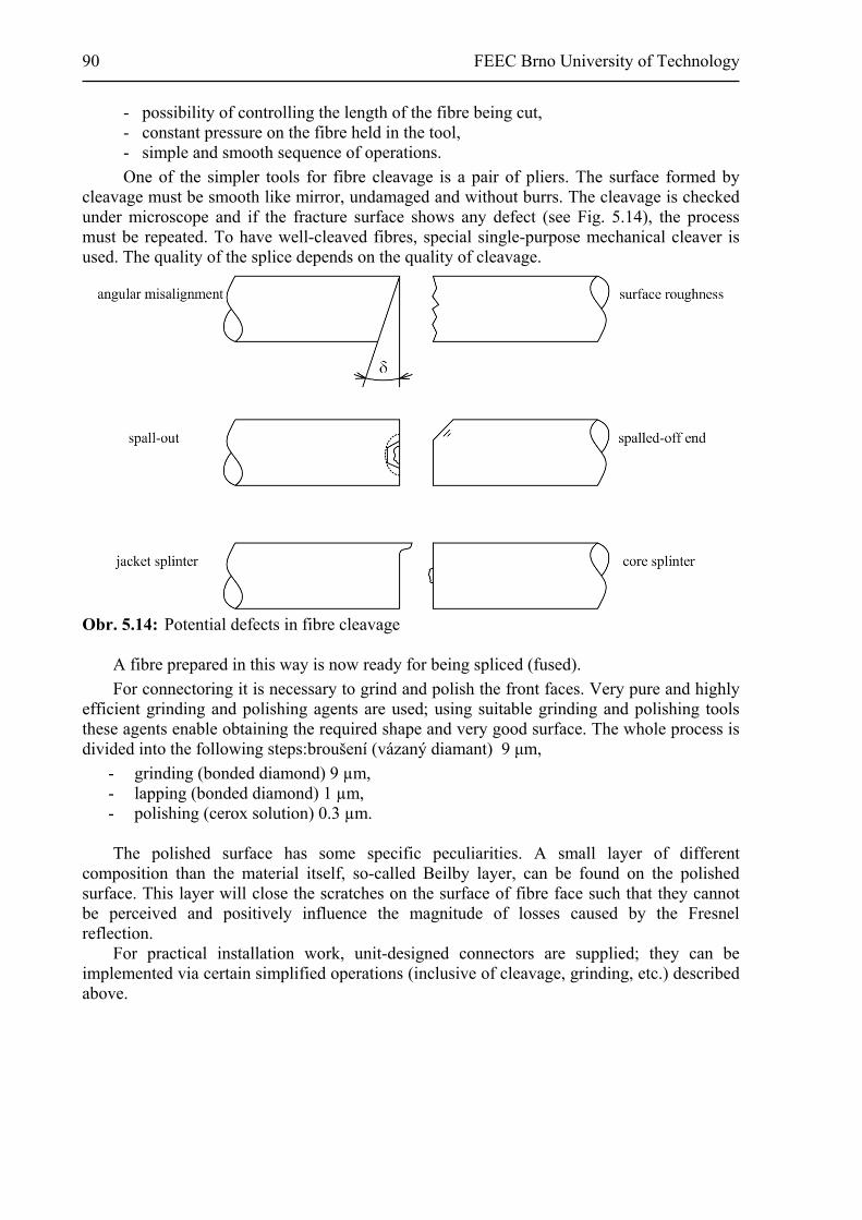
90 FEEC Brno University of Technology
- possibility of controlling the length of the fibre being cut, - constant pressure on the fibre held in the tool, - simple and smooth sequence of operations.
One of the simpler tools for fibre cleavage is a pair of pliers. The surface formed by cleavage must be smooth like mirror, undamaged and without burrs. The cleavage is checked under microscope and if the fracture surface shows any defect (see Fig. 5.14), the process must be repeated. To have well-cleaved fibres, special single-purpose mechanical cleaver is used. The quality of the splice depends on the quality of cleavage.
Obr. 5.14: Potential defects in fibre cleavage
A fibre prepared in this way is now ready for being spliced (fused).
For connectoring it is necessary to grind and polish the front faces. Very pure and highly efficient grinding and polishing agents are used; using suitable grinding and polishing tools these agents enable obtaining the required shape and very good surface. The whole process is divided into the following steps:broušení (vázaný diamant) 9 μm,
- grinding (bonded diamond) 9 µm, - lapping (bonded diamond) 1 µm, - polishing (cerox solution) 0.3 µm. The polished surface has some specific peculiarities. A small layer of different
composition than the material itself, so-called Beilby layer, can be found on the polished surface. This layer will close the scratches on the surface of fibre face such that they cannot be perceived and positively influence the magnitude of losses caused by the Fresnel reflection.
For practical installation work, unit-designed connectors are supplied; they can be implemented via certain simplified operations (inclusive of cleavage, grinding, etc.) described above.

Optoelectronics for telecommunications and informatics 91
5.2 Non-demountable splices
This group includes the most frequently applied method of fusion splicing, methods of joining optical fibres by gluing, and most recently the method of fixed metallic splices.
Fusion splicing
Arc welding has become the most widely spread among the existing methods. The method of gas welding and the CO2 laser method are used less frequently. Since the fibre cross-section must not be narrowed in the fusion splice, the fibres are moved against each other during fusing. These operations are very important for the splice quality and are usually checked automatically (using a microprocessor with I/O circuits). To get a good fusion splice, we must also know the melting point of glass. Depending on the type of glass the time of adjusting the fibre end and the time of welding must be set.
This is followed by cleavage of the fibre and removal of the primary coating (described in detail in 5.1).
To maintain axial alignment of fibres prior to fusion, wedge-shaped grooves are used, which guarantee the required fibre geometry during fusion. Surface tension in the area of the fusion zone provides for equal diameter of the fibres and the melt. The adjustment of fibres and the course of fusion phase can be followed under a microscope or on a screen. A simplified schematic diagram and principle of fusing optical fibres can be seen in Fig. 5.15. The fusion proper occurs at the moment when the distance between the fibres is ca. 20 µm. In about 0.2 s, when the fibre ends start melting, the fibres start moving towards each other and are pressed against each other with an overlap of ca. 15 µm. The total time of arc discharge is ca. 2.5 s. For example, for the fusion of multimode fibres, Ericsson Company gives an arc current of 16.25 mA/50 Hz and a total fusion time of 4 s.
Obr. 5.15: Principle of fusing optical fibres
After fusing the splice, the strength of the splice is tested and the splice is measured for attenuation.
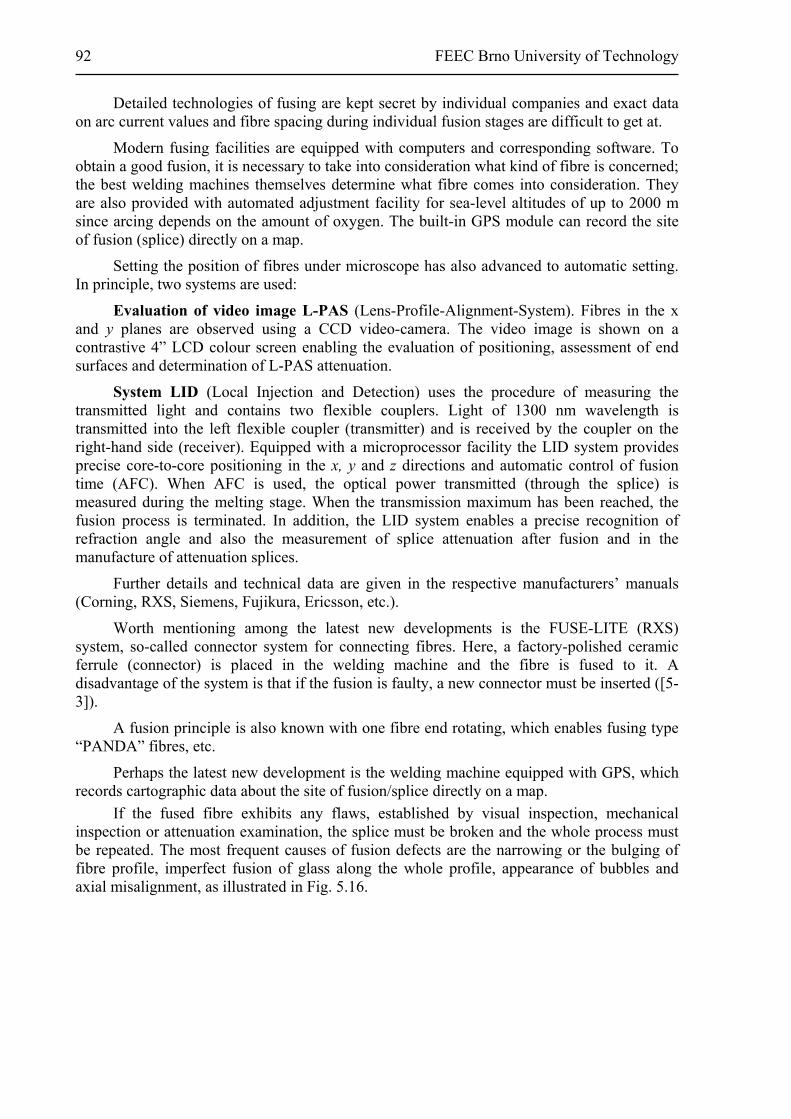
92 FEEC Brno University of Technology
Detailed technologies of fusing are kept secret by individual companies and exact data on arc current values and fibre spacing during individual fusion stages are difficult to get at.
Modern fusing facilities are equipped with computers and corresponding software. To obtain a good fusion, it is necessary to take into consideration what kind of fibre is concerned; the best welding machines themselves determine what fibre comes into consideration. They are also provided with automated adjustment facility for sea-level altitudes of up to 2000 m since arcing depends on the amount of oxygen. The built-in GPS module can record the site of fusion (splice) directly on a map.
Setting the position of fibres under microscope has also advanced to automatic setting. In principle, two systems are used:
Evaluation of video image L-PAS (Lens-Profile-Alignment-System). Fibres in the x and y planes are observed using a CCD video-camera. The video image is shown on a contrastive 4” LCD colour screen enabling the evaluation of positioning, assessment of end surfaces and determination of L-PAS attenuation.
System LID (Local Injection and Detection) uses the procedure of measuring the transmitted light and contains two flexible couplers. Light of 1300 nm wavelength is transmitted into the left flexible coupler (transmitter) and is received by the coupler on the right-hand side (receiver). Equipped with a microprocessor facility the LID system provides precise core-to-core positioning in the x, y and z directions and automatic control of fusion time (AFC). When AFC is used, the optical power transmitted (through the splice) is measured during the melting stage. When the transmission maximum has been reached, the fusion process is terminated. In addition, the LID system enables a precise recognition of refraction angle and also the measurement of splice attenuation after fusion and in the manufacture of attenuation splices.
Further details and technical data are given in the respective manufacturers’ manuals (Corning, RXS, Siemens, Fujikura, Ericsson, etc.).
Worth mentioning among the latest new developments is the FUSE-LITE (RXS) system, so-called connector system for connecting fibres. Here, a factory-polished ceramic ferrule (connector) is placed in the welding machine and the fibre is fused to it. A disadvantage of the system is that if the fusion is faulty, a new connector must be inserted ([5-3]).
A fusion principle is also known with one fibre end rotating, which enables fusing type “PANDA” fibres, etc.
Perhaps the latest new development is the welding machine equipped with GPS, which records cartographic data about the site of fusion/splice directly on a map.
If the fused fibre exhibits any flaws, established by visual inspection, mechanical inspection or attenuation examination, the splice must be broken and the whole process must be repeated. The most frequent causes of fusion defects are the narrowing or the bulging of fibre profile, imperfect fusion of glass along the whole profile, appearance of bubbles and axial misalignment, as illustrated in Fig. 5.16.

Optoelectronics for telecommunications and informatics 93
Obr. 5.16: Potential defects in fibre fusion
When the fusion has been completed, the primary coating of fibre must be renewed, e.g. using special silicone. The secondary coating is restored, for example, by applying a contractible plastic tube to the fusion site and heating it; the fibre thus gets firmly fixed at the fusion site and near it.
Mechanical strength of splices is about 70% of the strength of fibre, and the average value of optical attenuation is about 0.02 dB ([5-3]).
Glued splices In these splices, glue is used to fix the fibre to the substrate and to connect fibres to each other. The glue has the following functions:
- its refractive index is very similar to that of the fibre, - it protects the splice against environment, - it fixes permanently the fibres in required position, - it prevents splice deformations and provides tensile strength. The most frequently used type of splice consists of a sleeve whose inner diameter
corresponds to the outer diameter of the fibres being joined, and in which the touching fibre ends are glued together. Alternatively, the sleeve may contract thermoplastically or contain adhesive material that will set when exposed to UV radiation (see Fig. 5.17).
Obr. 5.17: Splicing of optical fibres in a sleeve

94 FEEC Brno University of Technology
The technique of hardenable splice is based on the introduction of ultraviolet light into the fibre after the splice geometry has been set. Due to the light, the glue polymerizes and meets all the above requirements.
Losses in these splices are about 0.1 dB, sometimes even less. The splices are sensitive to temperature changes. An additional loss of 0.1 dB may appear following the temperature cycle -30 °C - +70 °C.
Mechanical splices
It is obvious from the name itself that axial alignment of the fibre is obtained using various mechanical structures such as V-grooves (see Fig. 5.18), tunnels formed between blocks of bars, cylinders and corners of square profiles (Fig. 5.19). It is important that fibres prepared in this way should be fixed firmly to the flattening surface since they must withstand handling and environmental effects.
Obr. 5.18: Splice with V-groove
Obr. 5.19: Cylindrical splice
To obtain permanent optical losses below 0.3 dB it is necessary to use optical filler material between the fibre ends. This material is chosen depending on the optical properties of glass. They are usually silicone gels, epoxy resins and ultraviolet glues. Filler materials must remain in contact with both fibres even if the gap is changed. These materials serve at the same time as primary coating of bare core. In the case of glues, also the mechanical strength of the splice is ensured.
Optical losses of mechanical splices usually depend on temperature. At room temperature the characteristic value is 0.1 to 0.15 dB. A good splice has an additional loss of 0.05 dB after the temperature has changed from -40 °C to +60 °C, for less good splices it is 0.1 to 0.2 dB. Fast push-down metallic splices are the latest novelty introduced by Tyco Electronics under

Optoelectronics for telecommunications and informatics 95
the name Record Splice and by 3M Company under the name Fibrlok, for splicing multimode and single-mode fibres. After five years of development, a device has been fabricated that is cheap and easy to handle, giving very good splices with less than 0.1 dB attenuation, guaranteed for any splice; in fact, some 30% of splices achieve values below 0.02 dB. The device does not require any supply; it operates on the mechanical principle and can thus be deployed with advantage in explosion-hazard environments.
Installation of the splice proceeds sequentially in a device in the form of a portable suitcase. The first operation consists in removing insulation and primary coating, followed by making a cut in the fibre and cleavage. Gel is then applied to fibre ends (this reduces losses on the glass-air transition and also removes superficial defects from the fracture surface), which are then inserted into the push-down splice and, finally, joined by (hand-) exerted pressure. Splices realized in this way are of high quality, precise, fast and do not require much training on the part of personnel.
The price of this device is ca. one tenth of the purchase cost of a welding facility.
5.3 Demountable splices
Demountable splices, so-called connectored splices, are mostly used in exchanges or at sites of repeater amplifiers, to a less degree in cable routes where cables with ribbon structure are used.
The principle of connectors again consists in guiding precisely the respective ends of fibre lightguides against each other but the problem is complicated here in that the optimum position needs to be secured by a suitable mechanical stop and by joining the two connector parts. The fibres to be spliced must not touch each other in order to prevent abrasion of the front surfaces. Initial adjustment of the position of fibre ends with respect to the reference positions of the respective connector part plays an important role. Special fixing jigs or fast automatic micromanipulators are used to this end. The contact element is the main functional part of the connector and determines its quality and price.
ensure precise axial alignment of the fibres being spliced both rigid and flexible installation in the connector body are used. Most connectors use as the main design element inserted between the fibre and the adjustment mechanisms a suitable sleeve or pin or both. Losses in connectors of this type range between 0.2 and 0.6 dB, depending on the given design and the material used. There are diverse connector solutions differing in technology, design and material.
The principle of a simple co-axial connector is illustrated in Fig. 5.20. As can be seen, axial alignment is obtained using a calibrated quartz stone and a silicone rubber cone. The spacing between the ends of the two fibres in the stage of splicing is set by means of a metallic tube such that in the final position there is a small micrometer gap between the fibre ends. The fibre is fixed in the correct position by means of a plastic protection layer and by gluing. The connector in question is the first connector developed in the Czech Republic, in the Research Institute of Communication Technology in Prague.

96 FEEC Brno University of Technology
Obr. 5.20: Principle of the function of single-mode connector for splicing two optical fibres
Example of another possible connector solution is in Fig. 5.21. Arrow heads represent reference surfaces.
Obr. 5.21: Principle of fibre connector
The principle of single-mode connector is given in Fig. 5.22. The connector is terminated by a precise planar polished surface (quartz). In order to reduce losses the fibre is fixed with glues based on quartz – epoxy, which provide good mechanical integrity and broad thermal stability.
Obr. 5.22: Principle of precise (single-mode) connector
Fig. 5.23 shows a practical implementation of connector.
Obr. 5.23: Practical connector implementation
Connectors with ball lenses have recently come to be increasingly used because of their excellent transmission properties (see Chapter 5.1). The principle of the operation of this connector is shown in Fig. 5.24.

Optoelectronics for telecommunications and informatics 97
Obr. 5.24: Principle of connector with lenses
Fig. 5.25 shows a ribbon connector of the MT type, which can also cope with 2, 4, 6, 12, and 24 fibres. There are many variants of ribbon connector. Tyco Electronics supplies up to 72 fibres in one connector.
Obr. 5.25: Ribbon connector
Our leading manufacturer of optical connectors, OPTOKON Co. Ltd. Jihlava, manufactures various types of optical connector. One among the first types was type SMA optical connector. Connectors are fixed to the cable by the technology of pressing; they are all-metallic with stainless-steel guiding system. The terminal surface is polished and optically conducting. The connection thread is inch thread 1/4 - 36 – UNS – 28. Example of the connection part of optical connectors can be seen in Fig. 5.26. Examples of the current most frequently used connectors of the SC type by OPTOKON Co., Ltd., a leading manufacturer of connectors, are shown in Fig. 5.27 ([5-4]).
Obr. 5.26: Optical connector

98 FEEC Brno University of Technology
It is obvious from the figure how precise the requirements are that are placed on the mechanical and optical reference planes. An optical splice has a lifetime of minimally 1000 cycles. Attenuation of the connector is less than 0.3 dB.
Obr. 5.27: SC connector in PC version and adaptor
Connecting two connectors by a fibre or cable gives rise to an optical splicing fibre module. The optical splicing cable module is usually supplied in runs of 1, 2, 3, 5, 7, 10, 15, 20, 30, 50, and 70 m. An example can be seen in Fig. 5.28.
Obr. 5.28: Optical splicing module
Type FC connectors (complying with the IEC 86-B recommendation), designated 2WF 862, are designed for multimode fibres 50/125 GI. They are provided with a cylindrical guiding system of 2.5 mm in diameter and 7.5 mm in length. The joining parts are provided with M 8 x 0.75 thread. The connectors are provided with a stud that prevents their rotation. They are made of stainless steel, the elastic sleeve is of beryllium bronze, and the surface has nickel finish. The schematic diagram of the connector is given in Fig. 5.29. Connector attenuation is less than 0.3 dB till the end of mechanical lifetime, i.e. 1000 cycles.
Obr. 5.29: Optical connector, splice GI
The strict requirements on the manufacture of connectors are evident from the above data. In the last decade further types of optical connector have appeared on the market. It is

Optoelectronics for telecommunications and informatics 99
not possible to describe here in detail individual connectors as has been done hitherto; only some types of connector will be given below.
Since the time when connectors began to be used, their manufacturing technology has experienced many changes, which has primarily shown in the reduction of insertion attenuation and cost, increased resistance to polarization properties, and back scattering.
There are now more materials suitable for the manufacture of connectors, more methods of polishing, and a greater variety of designs.
Some simple types of connector can be installed on the fibre in the field (toolkit for the manufacture of connectors) while more complicated connectors are mostly bought from the manufacturers (OPTOKON, QOS, etc.) with a pigtail, which is fused to the route.
Ferrule types:
- Aluminium ferrule – brittle material, difficult polishing, great thermal expansion. - Zirconia ferrule – frequently used material, 4 times greater strength than in aluminium,
very good polish, small dimensions of ceramic grain, low friction wear. - Plastic ferrule – the cheapest type, easy polishing, higher attenuation, shorter lifetime - Composite ferrule – the best, most precise and most expensive ferrule, small insertion
attenuation losses. - ARCAP ferrule – cheap, easy polishing, low friction wear, long lifetime.
Possible ferrule terminations are shown in Fig. 5.30.
Obr. 5.30: Ferrule terminations
The effect of polishing on the value of back reflection is indicated in Fig. 5.31. The last to be given here, the APC (Angle Polish Connector) connector belongs to the best (and most expensive) connectors. The figure gives a detailed view of the PC and APC connector faces.
Obr. 5.31: Fibre terminations

100 FEEC Brno University of Technology
Connector types: - Bionic – one of the first connectors (1980) supported by the AT&T Co., conic ferrule,
insertion attenuation 0.5 – 0.6 dB. - SMA – also an older type of connector, ferrule not protected against rotation,
aluminium or ARCAP ferrule, threaded cap nut. - FC – standard for telecommunications, ceramic or composite ferrule of 2.5 mm in
diameter, threaded cap nut with positioning. - ST – standard for telecommunications, pin arrest against rotation, spring-mounted
ferrule, bayonet splice, insertion attenuation 0.2 – 0.3 dB. - SC – supported by AT&T, ISO/IEC11801, push-pull version, ceramic or composite
ferrule, insertion attenuation 0.15 dB. - FDDI – paired connector for FDDI networks, push-pull version, ceramic ferrule,
insertion attenuation 0.2 dB. - ESCON – similar to FDDI, supported by IBM. - E2000 – European standard for telecommunications, developed by DIAMOND Co.,
push-pull version, spring-mounted cover overlapping the ferrule, insertion attenuation 0.2 dB.
- LC – represents a new generation of connectors (in execution it resembles the SC connector) whose design takes up 50% less space in comparison with SC. It is manufactured in MM and SM variants. In the duplex version it is compatible with the dimensions of RJ-45 connectors.
- MT-RJ double-fibre connector, compatible with RJ 45, supported by AMP, HP, Fujikura, and Siecor.
- MTP – designed for ribbon cables 4, 6, 12, 24, and 36 to 72 fibres. - VF 45 – double-fibre connector, for PC connection, supported by 3M Co. for the
Volition system. Some connector versions were given above; further typical connectors are shown in Fig.
5.32.
Obr. 5.32: Optical connectors
The following connectors are designed for special applications: - HMA connectors, in which the optical ray is extended over a system of lenses so that
splicing takes place on a large area. The connector is resistant to vibrations, dust, and water. Its application is in the armed forces, heavy industry, mining, and oil industry but also in TV transmissions, etc.
From the viewpoint of the type of application (a maximum of 6 fibres, SM-MM) two basic types of interconnection modules are used:
a) Tactical military LD cable with OHMA connectors of the plug type at both ends, suitable for interconnecting network nodes (length 200 – 500 m). b) Hybrid modules for interconnection between OHMA connectors and standard optical connectors of the types SC, ST, LC, etc., designed for connection at terminal points of networks with standard outputs.
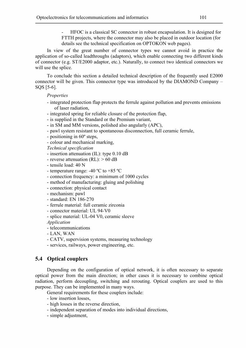
Optoelectronics for telecommunications and informatics 101
- HFOC is a classical SC connector in robust encapsulation. It is designed for FTTH projects, where the connector may also be placed in outdoor location (for details see the technical specification on OPTOKON web pages).
In view of the great number of connector types we cannot avoid in practice the application of so-called leadthroughs (adaptors), which enable connecting two different kinds of connector (e.g. ST/E2000 adaptor, etc.). Naturally, to connect two identical connectors we will use the splice.
To conclude this section a detailed technical description of the frequently used E2000 connector will be given. This connector type was introduced by the DIAMOND Company – SQS [5-6].
Properties
- integrated protection flap protects the ferrule against pollution and prevents emissions of laser radiation,
- integrated spring for reliable closure of the protection flap, - is supplied in the Standard or the Premium variant, - in SM and MM versions, polished also angularly (APC), - pawl system resistant to spontaneous disconnection, full ceramic ferrule, - positioning in 60º steps, - colour and mechanical marking,
Technical specification - insertion attenuation (IL): type 0.10 dB - reverse attenuation (RL): > 60 dB - tensile load: 40 N - temperature range: -40 ºC to +85 ºC - connection frequency: a minimum of 1000 cycles - method of manufacturing: gluing and polishing - connection: physical contact - mechanism: pawl - standard: EN 186-270 - ferrule material: full ceramic zirconia - connector material: UL 94-V0 - splice material: UL-04 V0, ceramic sleeve
Application - telecommunications - LAN, WAN - CATV, supervision systems, measuring technology - services, railways, power engineering, etc.
5.4 Optical couplers
Depending on the configuration of optical network, it is often necessary to separate optical power from the main direction; in other cases it is necessary to combine optical radiation, perform decoupling, switching and rerouting. Optical couplers are used to this purpose. They can be implemented in many ways. General requirements for these couplers include:
- low insertion losses, - high losses in the reverse direction, - independent separation of modes into individual directions, - simple adjustment,
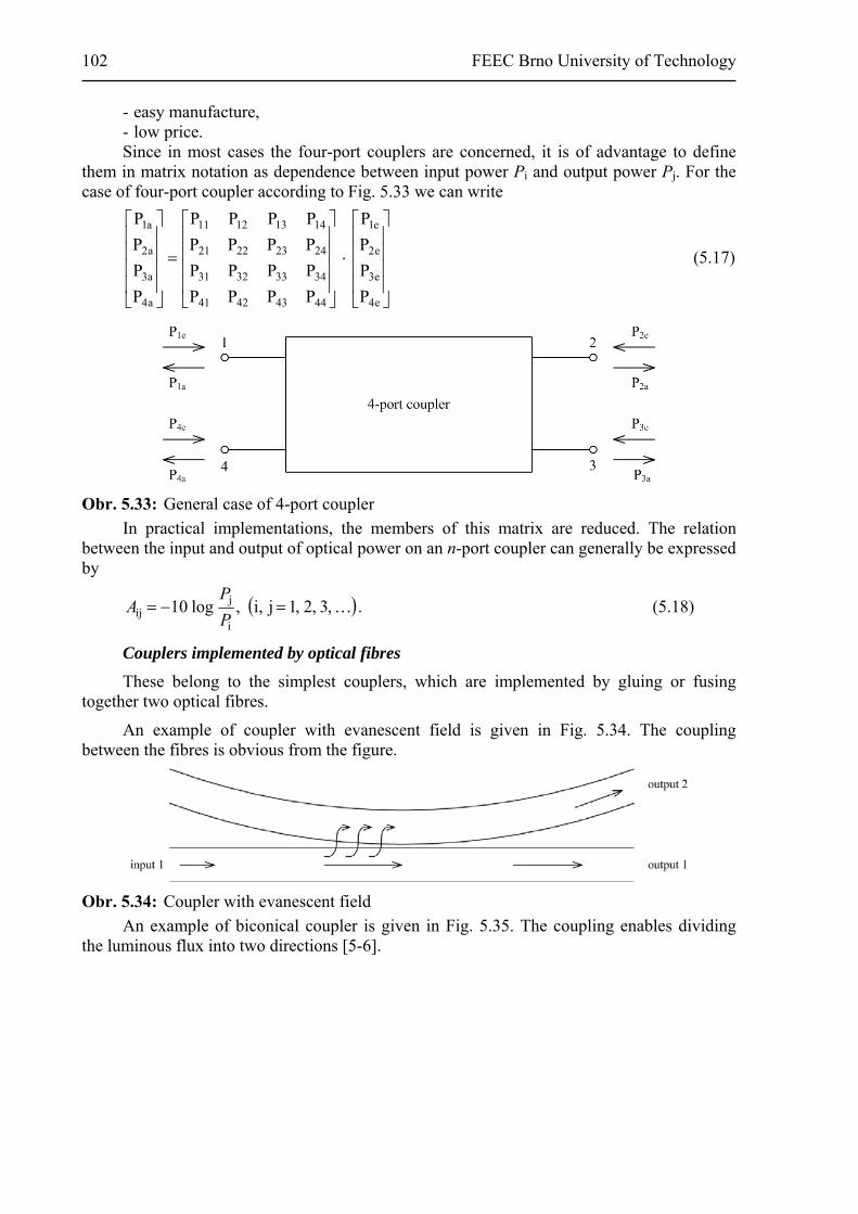
102 FEEC Brno University of Technology
- easy manufacture, - low price. Since in most cases the four-port couplers are concerned, it is of advantage to define
them in matrix notation as dependence between input power Pi and output power Pj. For the case of four-port coupler according to Fig. 5.33 we can write
e4
e3
e2
e1
44434241
34333231
24232221
14131211
a4
a3
a2
a1
P
P
P
P
PPPP
PPPP
PPPP
PPPP
P
P
P
P
(5.17)
Obr. 5.33: General case of 4-port coupler
In practical implementations, the members of this matrix are reduced. The relation between the input and output of optical power on an n-port coupler can generally be expressed by
,3,2,1j,i,log10i
jij
P
PA . (5.18)
Couplers implemented by optical fibres
These belong to the simplest couplers, which are implemented by gluing or fusing together two optical fibres.
An example of coupler with evanescent field is given in Fig. 5.34. The coupling between the fibres is obvious from the figure.
Obr. 5.34: Coupler with evanescent field
An example of biconical coupler is given in Fig. 5.35. The coupling enables dividing the luminous flux into two directions [5-6].

Optoelectronics for telecommunications and informatics 103
Obr. 5.35: Biconical coupling of optical fibres
Frequently applied couplers are directional couplers in the form of Y, as shown in Fig. 5.36. They are used to couple and decouple light in optical routes and in measuring technology. Light can be delivered either from fibre 1 to fibres 2 and 3 or vice versa. Fibres 2 and 3 are ground to the shape of Y.
Obr. 5.36: Y-coupler
The optical parameters are expressed by the matrix
dB
0
34
3
34
0
8,3
7,3
8,3
0
PS
. (5.19)
The slight difference in the division of powers in fibres 2 and 3 is due to the non-uniformity of grinding and gluing the two fibre halves.
Various couplings can be obtained by displacing the fibres axially against each other. In the case of step-index fibres, the coupling depends on the overlap of surfaces (see Fig. 5.37). Optical relays, switches, etc. operate on this principle. Fixing a fibre (fibres) to a metallic reed controlled by magnetic field (analogy to reed relays) will enable switching optical power in this way (see Fig. 5.38).
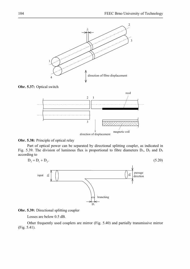
104 FEEC Brno University of Technology
Obr. 5.37: Optical switch
Obr. 5.38: Principle of optical relay
Part of optical power can be separated by directional splitting coupler, as indicated in Fig. 5.39. The division of luminous flux is proportional to fibre diameters D1, D2 and D3 according to
3 1 2D D D . (5.20)
Obr. 5.39: Directional splitting coupler
Losses are below 0.5 dB.
Other frequently used couplers are mirror (Fig. 5.40) and partially transmissive mirror (Fig. 5.41).
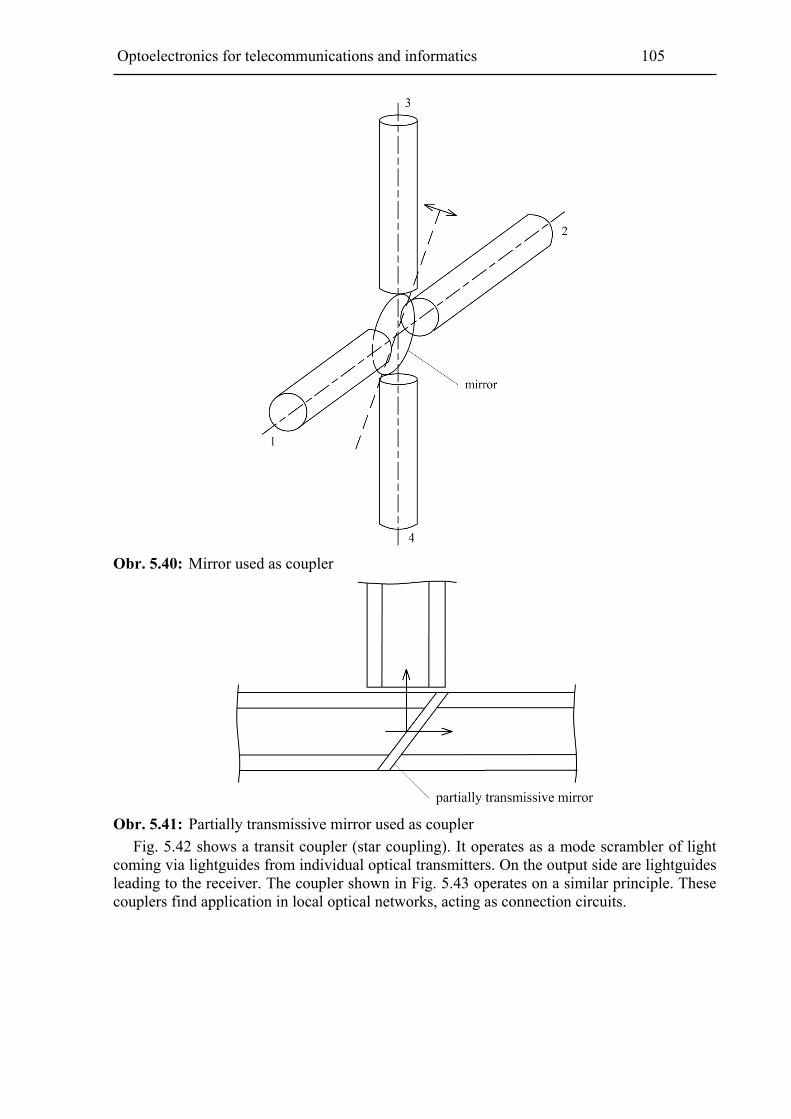
Optoelectronics for telecommunications and informatics 105
Obr. 5.40: Mirror used as coupler
Obr. 5.41: Partially transmissive mirror used as coupler
Fig. 5.42 shows a transit coupler (star coupling). It operates as a mode scrambler of light coming via lightguides from individual optical transmitters. On the output side are lightguides leading to the receiver. The coupler shown in Fig. 5.43 operates on a similar principle. These couplers find application in local optical networks, acting as connection circuits.
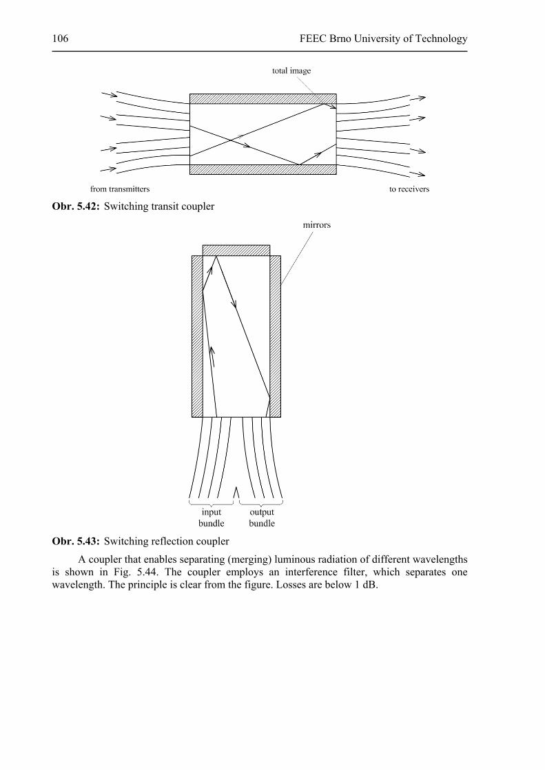
106 FEEC Brno University of Technology
Obr. 5.42: Switching transit coupler
Obr. 5.43: Switching reflection coupler
A coupler that enables separating (merging) luminous radiation of different wavelengths is shown in Fig. 5.44. The coupler employs an interference filter, which separates one wavelength. The principle is clear from the figure. Losses are below 1 dB.

Optoelectronics for telecommunications and informatics 107
Obr. 5.44: Wavelength coupler
These couplers can be used to implement duplex operation between two stations. They are sometimes referred to as wavelength division multiplexing (WDM). Most frequently used wavelengths are λ1 = 850 nm and λ2 = 1300 nm.
This brings us to the problems of mixing and separating various wavelengths from optical fibre. These problems will be dealt with in greater detail later.
6 Source of light
Radiation sources form one of the basic parts of optoelectronic telecommunication link. Although any source of light can in principle be used as a source of optical radiation, the application, for example, of an electric bulb is for present-day requirements out of the question because of its low energy and unfavourable radiation characteristics. In laboratories concerned with sources of radiation very intensive studies are therefore conducted into sources based on the solid phase that generate radiation at room temperature. These are semiconductor sources, with the focus on light-emitting diodes and laser diodes.
The main requirements placed on optical sources are the following: - maximum efficiency of the conversion of electrical energy to radiant energy, - generation of radiation on such wavelengths where the attenuation of current optical
fibres is the lowest, - generation of radiation at room temperature, - high reliability and long lifetime (problem of lasers), - easy modulation over a wide range, above all via changing the injection (supply)
current, - high monochromatism or coherence of generated radiation, - the narrowest possible directional characteristic of out-going radiation, - easy connectibility of generated radiation to optical fibre, - small dimensions and weight.

108 FEEC Brno University of Technology
For optical telecommunications the following types of sources come into consideration: - incoherent – light-emitting semiconductor diodes (LED - Light Emitting Diode)
coherent – lasers: mainly semiconductor diodes (LD – Laser Diode), for special purposes also gas, solid-state, and multiline lasers.
In first approximation, light-emitting diodes (LED) are cheap and easily available, with long lifetime and easy to modulate. However, they have a large divergence of the output beam and radiate a lower output (in comparison with LD) on all wavelengths that are suitable for telecommunication transmissions.
Laser semiconductor sources (LD) feature higher radiated output, lower spectral width, high efficiency of coupling to fibre, and the possibility of modulating to higher frequencies (GHz, Gbit.s-1). On the other hand, they require higher supply and temperature stabilization; they are the most likely cause of errors in optical routs (stand-by redundancy is introduced but their lifetime is steadily increasing) and are more expensive.
From the viewpoint of small dimensions, easy connection to optical fibre and easy modulation, the two elements (LED and LD) are frequently used in the telecommunication practice. For less demanding applications, where it is not necessary to maintain directionality of optical beam, and for transmissions over shorter distances the LED semiconductor sources are used. For transmissions over longer distances, where it is necessary to radiate in a narrow beam and where several wavelengths need to be transmitted (wavelength division multiplexing – WDM) the laser semiconductor diodes (LD) are used.
6.1 Light-emitting diodes
Semiconductor infrared electroluminescence diodes (LED) are P-N structures, mostly on the basis of GaAs, polarized in the forward direction. On the P-N junction minority carriers are injected, part of which do not combine radiantly. The simplest structure is shown schematically in Fig. 6.1.
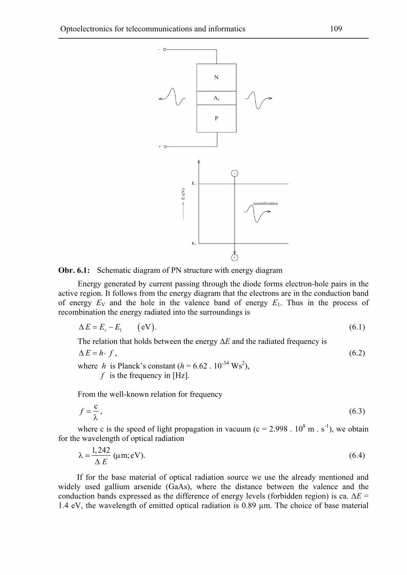
Optoelectronics for telecommunications and informatics 109
Obr. 6.1: Schematic diagram of PN structure with energy diagram
Energy generated by current passing through the diode forms electron-hole pairs in the active region. It follows from the energy diagram that the electrons are in the conduction band of energy EV and the hole in the valence band of energy E1. Thus in the process of recombination the energy radiated into the surroundings is
1 eV .vE E E (6.1)
The relation that holds between the energy ΔE and the radiated frequency is
,E h f (6.2)
where h is Planck’s constant (h = 6.62 . 10-34 Ws2), f is the frequency in [Hz].
From the well-known relation for frequency
cf , (6.3)
where c is the speed of light propagation in vacuum (c = 2.998 . 108 m . s-1), we obtain for the wavelength of optical radiation
1,242( m;eV).
E
(6.4)
If for the base material of optical radiation source we use the already mentioned and widely used gallium arsenide (GaAs), where the distance between the valence and the conduction bands expressed as the difference of energy levels (forbidden region) is ca. ΔE = 1.4 eV, the wavelength of emitted optical radiation is 0.89 µm. The choice of base material
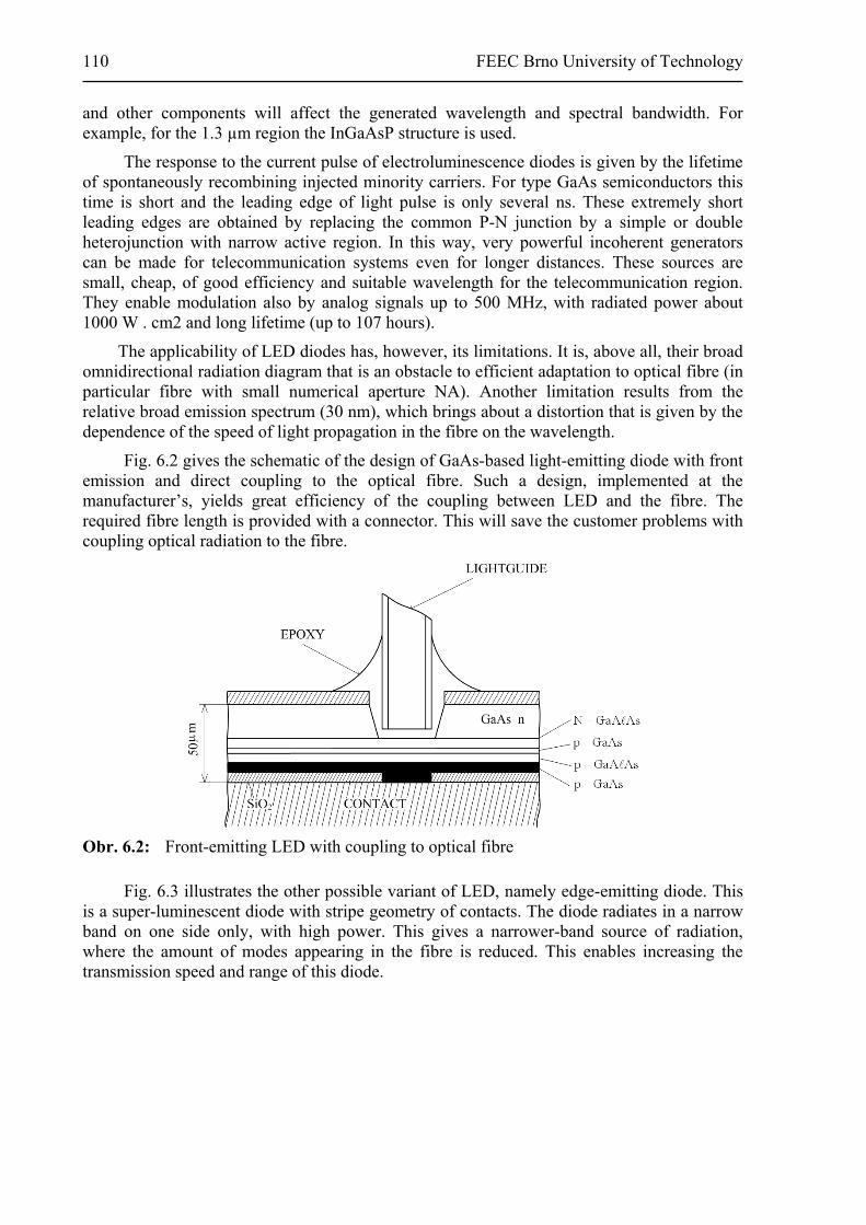
110 FEEC Brno University of Technology
and other components will affect the generated wavelength and spectral bandwidth. For example, for the 1.3 µm region the InGaAsP structure is used.
The response to the current pulse of electroluminescence diodes is given by the lifetime of spontaneously recombining injected minority carriers. For type GaAs semiconductors this time is short and the leading edge of light pulse is only several ns. These extremely short leading edges are obtained by replacing the common P-N junction by a simple or double heterojunction with narrow active region. In this way, very powerful incoherent generators can be made for telecommunication systems even for longer distances. These sources are small, cheap, of good efficiency and suitable wavelength for the telecommunication region. They enable modulation also by analog signals up to 500 MHz, with radiated power about 1000 W . cm2 and long lifetime (up to 107 hours).
The applicability of LED diodes has, however, its limitations. It is, above all, their broad omnidirectional radiation diagram that is an obstacle to efficient adaptation to optical fibre (in particular fibre with small numerical aperture NA). Another limitation results from the relative broad emission spectrum (30 nm), which brings about a distortion that is given by the dependence of the speed of light propagation in the fibre on the wavelength.
Fig. 6.2 gives the schematic of the design of GaAs-based light-emitting diode with front emission and direct coupling to the optical fibre. Such a design, implemented at the manufacturer’s, yields great efficiency of the coupling between LED and the fibre. The required fibre length is provided with a connector. This will save the customer problems with coupling optical radiation to the fibre.
Obr. 6.2: Front-emitting LED with coupling to optical fibre
Fig. 6.3 illustrates the other possible variant of LED, namely edge-emitting diode. This
is a super-luminescent diode with stripe geometry of contacts. The diode radiates in a narrow band on one side only, with high power. This gives a narrower-band source of radiation, where the amount of modes appearing in the fibre is reduced. This enables increasing the transmission speed and range of this diode.
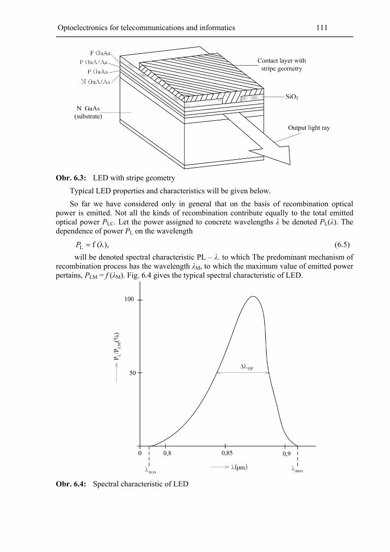
Optoelectronics for telecommunications and informatics 111
Obr. 6.3: LED with stripe geometry
Typical LED properties and characteristics will be given below.
So far we have considered only in general that on the basis of recombination optical power is emitted. Not all the kinds of recombination contribute equally to the total emitted optical power PLC. Let the power assigned to concrete wavelengths λ be denoted PL(λ). The dependence of power PL on the wavelength
),(fL P (6.5)
will be denoted spectral characteristic PL – λ. to which The predominant mechanism of recombination process has the wavelength λM, to which the maximum value of emitted power pertains, PLM = f (λM). Fig. 6.4 gives the typical spectral characteristic of LED.
Obr. 6.4: Spectral characteristic of LED
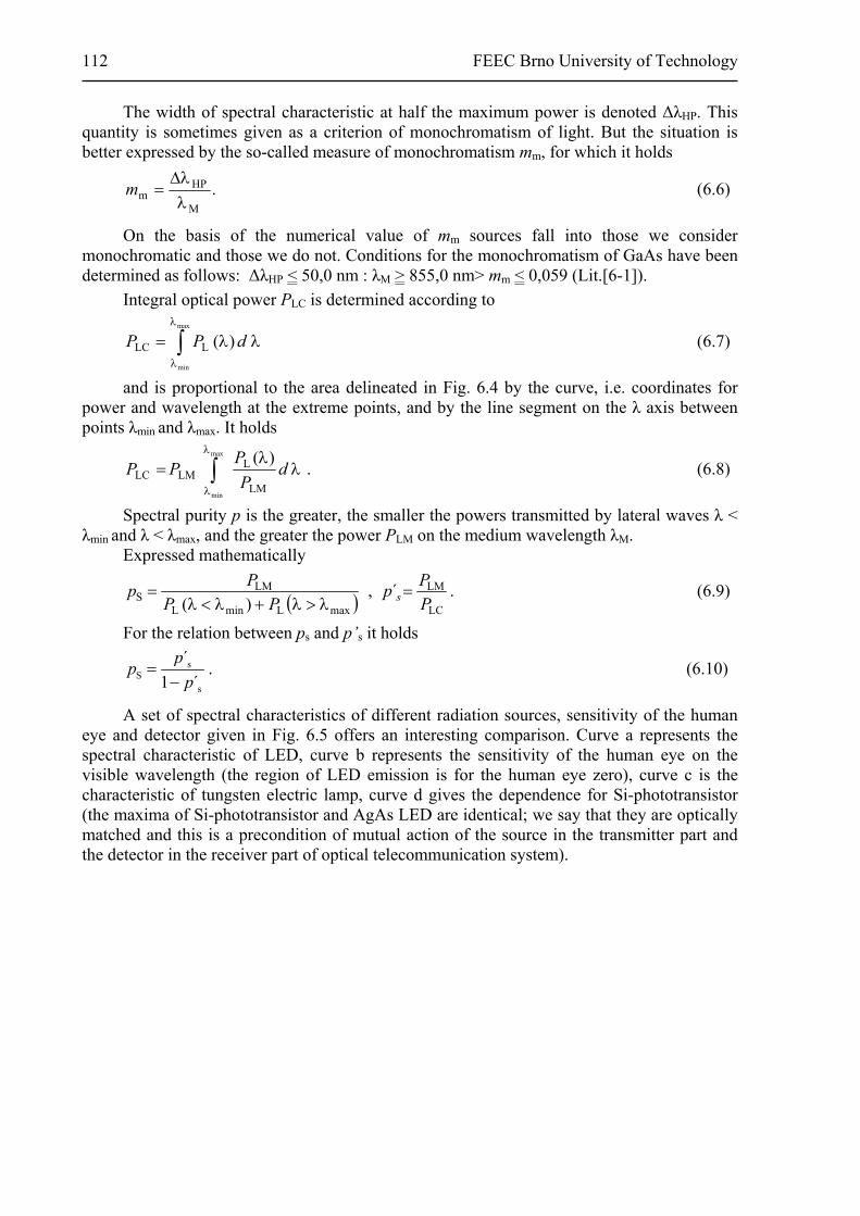
112 FEEC Brno University of Technology
The width of spectral characteristic at half the maximum power is denoted ΔλHP. This quantity is sometimes given as a criterion of monochromatism of light. But the situation is better expressed by the so-called measure of monochromatism mm, for which it holds
.M
HPm
m (6.6)
On the basis of the numerical value of mm sources fall into those we consider monochromatic and those we do not. Conditions for the monochromatism of GaAs have been determined as follows: ΔλHP < 50,0 nm : λM > 855,0 nm> mm < 0,059 (Lit.[6-1]).
Integral optical power PLC is determined according to
max
min
)(LLC dPP (6.7)
and is proportional to the area delineated in Fig. 6.4 by the curve, i.e. coordinates for power and wavelength at the extreme points, and by the line segment on the λ axis between points λmin and λmax. It holds
max
minLM
LLMLC
)(d
P
PPP . (6.8)
Spectral purity p is the greater, the smaller the powers transmitted by lateral waves λ < λmin and λ < λmax, and the greater the power PLM on the medium wavelength λM. Expressed mathematically
LC
LM
maxLminL
LMS ,
)( P
Pp
PP
Pp s
. (6.9)
For the relation between ps and p’s it holds
sS
s
´
1 ´
pp
p
. (6.10)
A set of spectral characteristics of different radiation sources, sensitivity of the human eye and detector given in Fig. 6.5 offers an interesting comparison. Curve a represents the spectral characteristic of LED, curve b represents the sensitivity of the human eye on the visible wavelength (the region of LED emission is for the human eye zero), curve c is the characteristic of tungsten electric lamp, curve d gives the dependence for Si-phototransistor (the maxima of Si-phototransistor and AgAs LED are identical; we say that they are optically matched and this is a precondition of mutual action of the source in the transmitter part and the detector in the receiver part of optical telecommunication system).

Optoelectronics for telecommunications and informatics 113
Obr. 6.5: Relative spectral characteristics
Electrooptic characteristic PL = f(PD) renders the dependence of optical power PL on electrical input of the diode PD = UFIF. Typical dependence is given in Fig. 6.6.
Obr. 6.6: Optical power vs. current
Quantum efficiency is established from the relation
L
D
.P
ηP
(6.11)

114 FEEC Brno University of Technology
Polar radiation plot of diodes is given as an example in Fig. 6.7.
Obr. 6.7: Polar radiation plot of LED
Of no less importance are the dynamic properties of LED, defined by the response of light to a jump in current. Rise time is the time necessary for the optical power to increase from the 10% of peak value of PLM to 90% (it is usually about 1 ns). Delay time is the time between the pulse beginning and the moment when PL reaches 10% of the maximum value. These times depend on the dynamic of recombination processes, on the junction capacity and on parasitic capacities of the casing and leads.
To a certain extent, light-emitting diodes depend on the supply current (spectral characteristic gets shifted towards higher wavelengths), which may lead to a change in temperature.
Exact values of the parameters and characteristics for individual types of light-emitting semiconductor diodes can be found in manufacturers’ catalogues.
6.2 Laser diodes
The laser diode (LD – Light Amplification by Stimulated Emission of Radiation Diode) is based, as the name itself suggests, on the amplification of light via stimulated emission of radiation.
In its design the laser diode does not differ much from the lay-out of edge-emitting LED but, in addition, it must meet some requirements that enable emitting coherent radiation.
In the following, only the basic principle of the laser function will be described; for in-depth study the reader is referred to [6-1] and [6-2].
The laser consists of two basic parts: - wavelength amplifier, - feedback resonator.
In the interaction of electromagnetic field with a solid, three basic types of junction between the fundamental and the excited state appear, namely absorption of radiation (junction to a higher energy state) and spontaneous and stimulated emissions (junction from

Optoelectronics for telecommunications and informatics 115
the excited state to the fundamental state). Spontaneous emission of radiation begins spontaneously and randomly some time (about 10-8 s) after excitation. Stimulated emission is triggered by direct interaction with the standing electromagnetic field. Due to this interaction the optical radiation originating in the element in which this type of junction predominates is coherent.
To achieve this effect, external energy must be applied to ensure such an out-of-equilibrium state where the number of atoms or molecular systems of the active region in excited state will be greater than in the basic state. Then in such a structure of the active region the predominant interaction between the field and the substance is stimulated emission and not absorption, and the optical radiation propagating in this region is amplified. This state is referred to as population inversion.
In population inversion the speed of emission transitions Wemission must be greater than the speed of absorption Wabsorption. In keeping with the energy levels the speed of emission will be proportional to
c c v v~ ( ) ( ) ( - υ)[1- ( - υ)]emiseW n W F W n W h F W h dW. (6.12)
v v c c~ ( - υ) F ( - υ) ( )[1 ( )]absorpceW n W h W h n W F W dW, (6.13)
where Fc and Fv are the Fermi-Dirac distribution functions
cFc
1( ) .
1 expF W p
W W
kT
(6.14)
vFv
1( ) ,
( )1 exp
F W hW h W
kT
where hυ is the energy of emitted photons nc, nv are the state densities in the conduction and valence bands, WFc, WFv are apparent Fermi levels valid for the conduction and valence bands. An important relation follows from conditions (6.12) and (6.13) for the amplification of optical radiation
Fc Fv υ.W W h (6.15)
The above relation is generally valid for semiconductors or for a medium that can amplify light of frequency υ. At the same time it is a necessary condition for light amplification but not sufficient for light generation. For the latter it is necessary to satisfy the feedback condition for the appearance of oscillations, i.e. to prepare a structure that enables introducing positive feedback with a sufficient feedback factor. The resonance properties of the Fabry-Perot cavity (see Fig. 6.8) are used for this purpose. In principle, this cavity is formed by two parallel partially transmitting mirrors placed at a distance LR on opposite sides of the semiconductor material, with the active region between them.

116 FEEC Brno University of Technology
Obr. 6.8: Schematic of semiconductor laser
The feedback condition can be written as
R
1n ( ) ,g L
R (6.16)
where R is the coefficient of mirror reflection, α is the coefficient of optical losses, g is the gain of active medium, LR is the length of resonator. Equation (6.16) is used to establish the threshold gain of active medium necessary for the generation of coherent light
prahR
1 1ln .g
L R
(6.17)
With the simplification that the Fabry-Perot cavity is a one-dimensional resonator in which the optical wave propagates in axial direction, the basic selection of modes is given by the requirement of integer number of half-waves between the reflection surfaces
R ,2
m Ln
(6.18)
where m is 1, 2, 3, …, λ is the wavelength,
Optoelectronics for telecommunications and informatics 117
n is the refractive index of cavity medium. For practical applications, for the purpose of achieving radiation directionality, the resonator is usually partially transmitting from one side only. Inciting the semiconductor laser structures by injection on the P-N junction is the simplest and most efficient method of achieving population inversion. Of practical importance are lasers based on double heterojunction. The optical field and the minority carriers are concentrated very effectively in a very narrow active region. The Fabry-Perot resonator is often replaced by a better resonator, as is the case of laser with distributed feedback (DFB) or laser with the Bragg reflection (Distributed Bragg Reflector); the schematic of the latter is given in Fig. 6.9. The indicated optical grating forms a frequency-selective reflector.
Obr. 6.9: Semiconductor laser with Bragg reflection
It is evident that the design of LD will affect the characteristics of radiant energy balance, spectral dependence, temperature dependence, etc.
A typical spectral characteristic of laser diode is shown in Fig. 6.10. Even in the case of sharp resonator tuning to the wavelength λM the radiant intensity does not pertain to only a single wavelength (absolute monochromatism) but is divided continuously in a certain interval of wavelengths. The radiant intensity (power) increases with increasing current. Increasing temperature will shift the spectral characteristic to higher wavelengths.

118 FEEC Brno University of Technology
Obr. 6.10: Spectral characteristic of laser
Another important laser characteristic is the dependence of emitted optical power on the amplitude of current. The graph of this function, PL = f (IM), is given in Fig. 6.11. It is apparent from the graph that with increasing temperature the characteristic gets shifted. It can also be seen that the characteristics are almost ideally linear so that in pulse operation the current amplitude modulation of luminous flux can be used.
Obr. 6.11: Dependence of emitted optical power on current amplitude
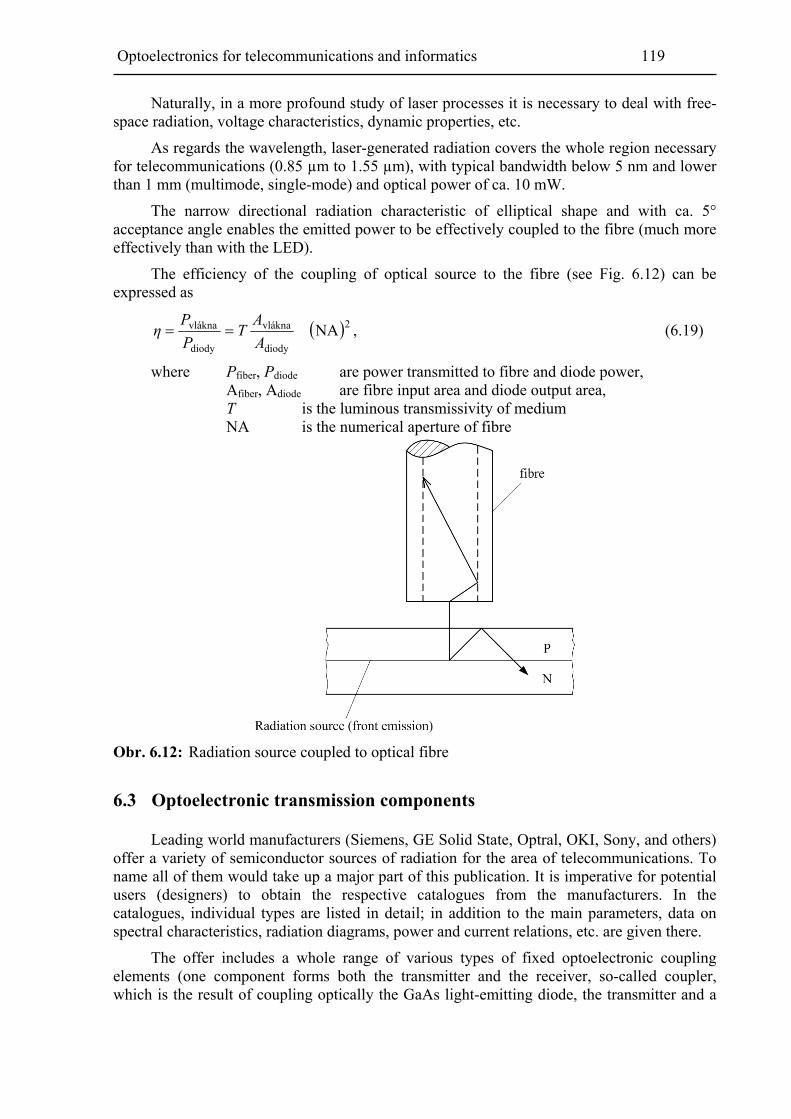
Optoelectronics for telecommunications and informatics 119
Naturally, in a more profound study of laser processes it is necessary to deal with free-space radiation, voltage characteristics, dynamic properties, etc.
As regards the wavelength, laser-generated radiation covers the whole region necessary for telecommunications (0.85 µm to 1.55 µm), with typical bandwidth below 5 nm and lower than 1 mm (multimode, single-mode) and optical power of ca. 10 mW.
The narrow directional radiation characteristic of elliptical shape and with ca. 5° acceptance angle enables the emitted power to be effectively coupled to the fibre (much more effectively than with the LED).
The efficiency of the coupling of optical source to the fibre (see Fig. 6.12) can be expressed as
2diody
vlákna
diody
vlákna NAA
AT
P
Pη , (6.19)
where Pfiber, Pdiode are power transmitted to fibre and diode power, Afiber, Adiode are fibre input area and diode output area, T is the luminous transmissivity of medium NA is the numerical aperture of fibre
Obr. 6.12: Radiation source coupled to optical fibre
6.3 Optoelectronic transmission components
Leading world manufacturers (Siemens, GE Solid State, Optral, OKI, Sony, and others) offer a variety of semiconductor sources of radiation for the area of telecommunications. To name all of them would take up a major part of this publication. It is imperative for potential users (designers) to obtain the respective catalogues from the manufacturers. In the catalogues, individual types are listed in detail; in addition to the main parameters, data on spectral characteristics, radiation diagrams, power and current relations, etc. are given there.
The offer includes a whole range of various types of fixed optoelectronic coupling elements (one component forms both the transmitter and the receiver, so-called coupler, which is the result of coupling optically the GaAs light-emitting diode, the transmitter and a

120 FEEC Brno University of Technology
silicon NPN phototransistor as the receiver) employed to galvanically separate current circuits.
7 Light modulation and detection
It is clear that transmitting information by means of optical radiation is only possible if the luminous flux is influenced one way or another. In keeping with the signal transmitted we speak of modulation while the reverse process is called demodulation. At the receiver end an optical detector must be connected which converts optical radiation back to electric signal.
7.1 Modulation methods
In optical transmission, too, generally known modulation methods are used, such as amplitude, frequency, and phase modulations. In the transmission of analog signals amplitude modulation with direct modulation of radiant intensity (AM-IM) is mostly used or also frequency modulation using the carrier frequency. Analog transmission methods are used with advantage in the transmission of TV signal. In the receiver it is then necessary to evaluate the changes in intensity, and in the demodulator to restore the original signal. For the transmission the original analogue signal can be converted to digital signal and the PCM-IM, PFM-IM, and PWM-IM modulation principles can be used.
When analogue modulation of the transmitting element is used, the relatively good linear dependence of transmitted power on excitation current is made use of. In comparison with digital transmission the requirements for signal-to-noise ratio are stricter and, also, the linearity of the attenuation and the phase characteristics need to be taken into consideration.
Modulation properties of LD
An advantage of semiconductor lasers is that direct modulation can be used, i.e. modulation current can be superimposed directly on the constant injection current, which sets the operating point on the output characteristic.
In analogue modulation it is of advantage to set the bias voltage just above the threshold current. In analyses made for a small modulation signal ([7-1], [7-2]), a mathematical representation was proposed, which is given by a system of two non-linear differential equations. From the two equations the following conclusions can be drawn: in the modulation characteristic a resonance peak can be expected as a result of the interaction of photon population and concentration of injected electrons. For excitation current I the resonance frequency fr is given approximately by
1
2p
re f p
1 1MHz ,
2
I If
I
(7.1)
where τe is the lifetime of electrons, τf is the lifetime of photons, Ip is the threshold current.
If typical values for the semiconductor laser are considered, e.g. Ip = 190 mA, τe = 4 ns, τf = 1 ps, and the laser is excited by the constant current I = 205 mA, we obtain from (7.1) fr = 7.07 . 108 Hz. The frequency response of a laser with the above parameters is shown in Fig. 7.1.
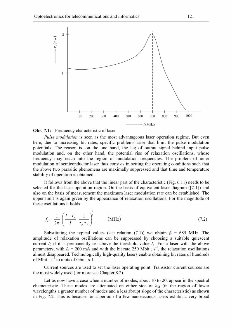
Optoelectronics for telecommunications and informatics 121
Obr. 7.1: Frequency characteristic of laser
Pulse modulation is seen as the most advantageous laser operation regime. But even here, due to increasing bit rates, specific problems arise that limit the pulse modulation potentials. The reason is, on the one hand, the lag of output signal behind input pulse modulation and, on the other hand, the potential rise of relaxation oscillations, whose frequency may reach into the region of modulation frequencies. The problem of inner modulation of semiconductor laser thus consists in setting the operating conditions such that the above two parasitic phenomena are maximally suppressed and that time and temperature stability of operation is obtained.
It follows from the above that the linear part of the characteristic (Fig. 6.11) needs to be selected for the laser operation region. On the basis of equivalent laser diagram ([7-1]) and also on the basis of measurement the maximum laser modulation rate can be established. The upper limit is again given by the appearance of relaxation oscillations. For the magnitude of these oscillations it holds
.MHz1
2
1 2
1
fe
pr I
IIf
(7.2)
Substituting the typical values (see relation (7.1)) we obtain fr = 685 MHz. The amplitude of relaxation oscillations can be suppressed by choosing a suitable quiescent current I0 if it is permanently set above the threshold value Ip. For a laser with the above parameters, with I0 = 200 mA and with the bit rate 250 Mbit . s-1, the relaxation oscillations almost disappeared. Technologically high-quality lasers enable obtaining bit rates of hundreds of Mbit . s-1 to units of Gbit . s-1.
Current sources are used to set the laser operating point. Transistor current sources are the most widely used (for more see Chapter 8.2).
Let us now have a case when a number of modes, about 10 to 20, appear in the spectral characteristic. These modes are attenuated on either side of λM (in the region of lower wavelengths a greater number of modes and a less abrupt slope of the characteristic) as shown in Fig. 7.2. This is because for a period of a few nanoseconds lasers exhibit a very broad

122 FEEC Brno University of Technology
radiation spectrum if they are operated with pulse modulation with bias voltage below the threshold of stimulated radiation. It is the result of the big jump in electron density in the time intervals between peaks of attenuated output oscillations of the laser. This high density of electrons provides sufficient gain to give rise to a number of modes. This phenomenon can be prevented by introducing a constant injection current whose value is just above its threshold.
Obr. 7.2: Spectral characteristic of laser
Modulation properties of LED
Light-emitting diodes can with advantage be modulated also internally, i.e. with the aid of injection current. Extensive use is made of the linear static modulation characteristic, which gets curved only at higher current values, due to thermal phenomena (see Fig. 6.6).
Due to the dynamic properties of LED (lifetime of injected electrons, voltage dependence of the p-n junction capacity) there is a delay in the diode response with respect to the injection current, and the leading and trailing edges of input modulation pulses are slowed down. These phenomena then limit the modulation frequency band. The maximum modulation frequency is approximately determined from the relation [7-1]
1.
2 e
f
(7.3)
Substituting again the typical values τe = 1 to 2 ns (lifetime of injected electrons) yields the maximum modulation frequency of LED in the range from 100 to 200 MHz.
In order to achieve higher modulation limits in pulse modulation, and for this purpose also to shorten the time delay te between the excitation jump current Ie and the appearance of output radiation, it is necessary to polarize the LED with a voltage whose value is close to the diffusion voltage ud. The modulation properties of LED are determined to a great extent by the design of the LED itself. And last but not least, it is necessary to properly match the generator output impedance with the low input impedance of the diode.
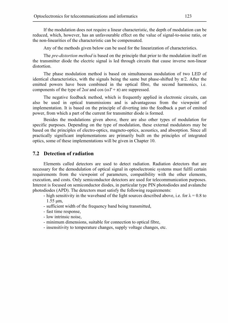
Optoelectronics for telecommunications and informatics 123
If the modulation does not require a linear characteristic, the depth of modulation can be reduced, which, however, has an unfavourable effect on the value of signal-to-noise ratio, or the non-linearities of the characteristic can be compensated.
Any of the methods given below can be used for the linearization of characteristics.
The pre-distortion method is based on the principle that prior to the modulation itself on the transmitter diode the electric signal is led through circuits that cause inverse non-linear distortion.
The phase modulation method is based on simultaneous modulation of two LED of identical characteristics, with the signals being the same but phase-shifted by π/2. After the emitted powers have been combined in the optical fibre, the second harmonics, i.e. components of the type of 2ωt and cos (ωT + π) are suppressed.
The negative feedback method, which is frequently applied in electronic circuits, can also be used in optical transmissions and is advantageous from the viewpoint of implementation. It is based on the principle of diverting into the feedback a part of emitted power, from which a part of the current for transmitter diode is formed.
Besides the modulations given above, there are also other types of modulation for specific purposes. Depending on the type of modulation, these external modulators may be based on the principles of electro-optics, magneto-optics, acoustics, and absorption. Since all practically significant implementations are primarily built on the principles of integrated optics, some of these implementations will be given in Chapter 10.
7.2 Detection of radiation
Elements called detectors are used to detect radiation. Radiation detectors that are necessary for the demodulation of optical signal in optoelectronic systems must fulfil certain requirements from the viewpoint of parameters, compatibility with the other elements, execution, and costs. Only semiconductor detectors are used for telecommunication purposes. Interest is focused on semiconductor diodes, in particular type PIN photodiodes and avalanche photodiodes (APD). The detectors must satisfy the following requirements:
- high sensitivity in the waveband of the light sources described above, i.e. for λ = 0.8 to 1.55 μm,
- sufficient width of the frequency band being transmitted, - fast time response, - low intrinsic noise, - minimum dimensions, suitable for connection to optical fibre, - insensitivity to temperature changes, supply voltage changes, etc.

124 FEEC Brno University of Technology
Obr. 7.3: Absorption of various detector materials
The detectors used are thus mostly elements with p-n junction. They are based on separating pairs of charge carriers, i.e. electrons and holes, which result from optical radiation being absorbed by the detector. Materials that have sufficient light absorbance in the above wavelength band are Ge, Si, GaAs, InGaAsP, and InGaAs. Their spectral coefficients of absorption αa are given in Fig. 7.3. The figure also gives the corresponding depth of radiation penetration into the material x0, which is defined by the relation
a
01
x (7.4)
When radiation of power P0 hits the detector surface, the process of absorption is given by the relation
a-α xOx 1 1 e ,P R P (7.5)
where R is the coefficient of detector surface reflection. This coefficient gives the magnitude of the part of incident power that does not penetrate into the semiconductor and is thus lost for useful processing. To prevent this and to enhance the overall detection efficiency, an antireflection layer of λ/4 thickness is applied to the functional surface of detector. The layer acts like an impedance transformer ([7-1]).
Relation (7.5) reveals the physical significance of penetration depth x0: it is a depth for which (7.4) holds, i.e. it is the distance from the detector surface, where 63% of incident power is absorbed.
From Fig. 7.3 we can also read the frequency limitation of application for individual materials. All the materials mentioned have a clearly expressed limit wavelength of application. For GaAs it is about 0.9 μm, for Si 1.1 μm, for InGaAsP 1.2 to 1.6 μm, and for Ge 1.7 μm.
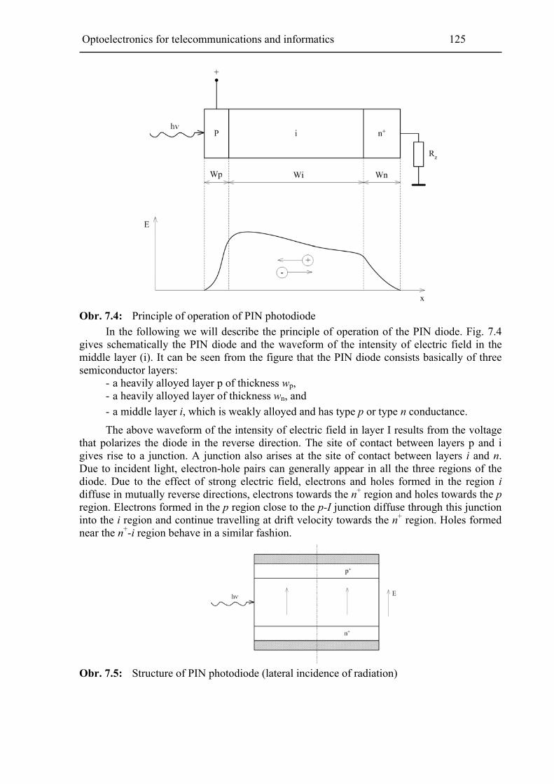
Optoelectronics for telecommunications and informatics 125
Obr. 7.4: Principle of operation of PIN photodiode
In the following we will describe the principle of operation of the PIN diode. Fig. 7.4 gives schematically the PIN diode and the waveform of the intensity of electric field in the middle layer (i). It can be seen from the figure that the PIN diode consists basically of three semiconductor layers:
- a heavily alloyed layer p of thickness wp, - a heavily alloyed layer of thickness wn, and
- a middle layer i, which is weakly alloyed and has type p or type n conductance.
The above waveform of the intensity of electric field in layer I results from the voltage that polarizes the diode in the reverse direction. The site of contact between layers p and i gives rise to a junction. A junction also arises at the site of contact between layers i and n. Due to incident light, electron-hole pairs can generally appear in all the three regions of the diode. Due to the effect of strong electric field, electrons and holes formed in the region i diffuse in mutually reverse directions, electrons towards the n+ region and holes towards the p region. Electrons formed in the p region close to the p-I junction diffuse through this junction into the i region and continue travelling at drift velocity towards the n+ region. Holes formed near the n+-i region behave in a similar fashion.
Obr. 7.5: Structure of PIN photodiode (lateral incidence of radiation)
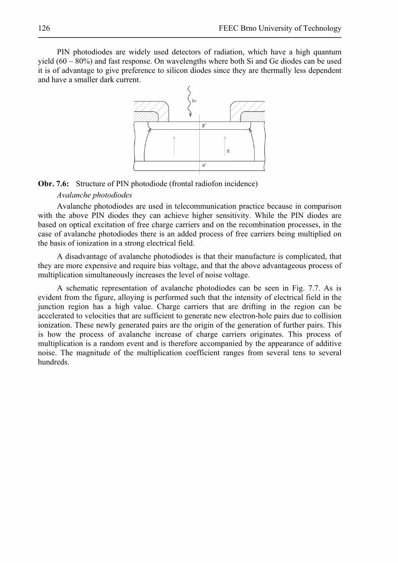
126 FEEC Brno University of Technology
PIN photodiodes are widely used detectors of radiation, which have a high quantum yield (60 – 80%) and fast response. On wavelengths where both Si and Ge diodes can be used it is of advantage to give preference to silicon diodes since they are thermally less dependent and have a smaller dark current.
Obr. 7.6: Structure of PIN photodiode (frontal radiofon incidence)
Avalanche photodiodes
Avalanche photodiodes are used in telecommunication practice because in comparison with the above PIN diodes they can achieve higher sensitivity. While the PIN diodes are based on optical excitation of free charge carriers and on the recombination processes, in the case of avalanche photodiodes there is an added process of free carriers being multiplied on the basis of ionization in a strong electrical field.
A disadvantage of avalanche photodiodes is that their manufacture is complicated, that they are more expensive and require bias voltage, and that the above advantageous process of multiplication simultaneously increases the level of noise voltage.
A schematic representation of avalanche photodiodes can be seen in Fig. 7.7. As is evident from the figure, alloying is performed such that the intensity of electrical field in the junction region has a high value. Charge carriers that are drifting in the region can be accelerated to velocities that are sufficient to generate new electron-hole pairs due to collision ionization. These newly generated pairs are the origin of the generation of further pairs. This is how the process of avalanche increase of charge carriers originates. This process of multiplication is a random event and is therefore accompanied by the appearance of additive noise. The magnitude of the multiplication coefficient ranges from several tens to several hundreds.
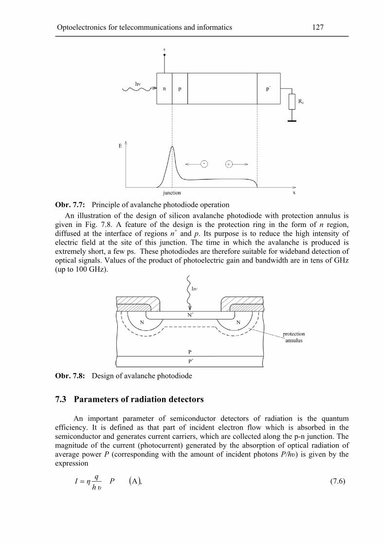
Optoelectronics for telecommunications and informatics 127
Obr. 7.7: Principle of avalanche photodiode operation
An illustration of the design of silicon avalanche photodiode with protection annulus is given in Fig. 7.8. A feature of the design is the protection ring in the form of n region, diffused at the interface of regions n+ and p. Its purpose is to reduce the high intensity of electric field at the site of this junction. The time in which the avalanche is produced is extremely short, a few ps. These photodiodes are therefore suitable for wideband detection of optical signals. Values of the product of photoelectric gain and bandwidth are in tens of GHz (up to 100 GHz).
Obr. 7.8: Design of avalanche photodiode
7.3 Parameters of radiation detectors
An important parameter of semiconductor detectors of radiation is the quantum efficiency. It is defined as that part of incident electron flow which is absorbed in the semiconductor and generates current carriers, which are collected along the p-n junction. The magnitude of the current (photocurrent) generated by the absorption of optical radiation of average power P (corresponding with the amount of incident photons P/hυ) is given by the expression
,APυh
qηI (7.6)

128 FEEC Brno University of Technology
where η is the quantum efficiency. Relation (7.6) allows estimating the sensitivity of a typical PIN diode: expressing the sensitivity Ad as a ratio of incident photocurrent to optical power, then
.A.W 1υh
qη
P
IAd (7.7)
(In the expression, h = 6,626.10-34 is Planck’s constant, q = 1,6 .10-19 C is the charge of electron.)
The frequency properties are influenced primarily by the photodiode design. From the viewpoint of detector connection it is necessary to know the impedance and time constants of the detector.
Relative spectral sensitivity is a dimensionless quantity. It gives the ratio of spectral sensitivity at a given wavelength to spectral sensitivity at maximum dependence.
No less important parameters are the dark current with non-illuminated detector, and the temperature dependence of detectors.
Another important parameter is the level of noise voltage. It determines the minimum value of detected power of incident radiation. The quantity PNEP (NEP – noise equivalent power) is introduced for this purpose. This power is defined as the power of incident radiation that generates on the detector the same effective voltage value as the noise voltage. The incident radiation is assumed to be sine-modulated. The value of PNEP is established by measuring the noise properties of detector and is obtained from the relation [1-2]
,W.Hz 1/2
f
šDNEP
Uf
UPP (7.8)
where Us is the effective value of noise voltage (V),
Uf is the effective value of photovoltage (V),
Δf is the amplifier bandwidth (Hz),
PD is the optical power incident on detector surface; effective value is
considered (W).
The effective value of noise voltage depends on the bandwidth of selective amplifier. In most cases it is recalculated for the 1 Hz width. For practical purposes and for the comparison of detectors the concepts of detectivity D and normalized detectivity Dn have been introduced, which are given by the relations
,:1
SDDP
D nNEP
(7.9)
where S is the detector surface (m2).
In Tables, for example, the designation D (0.85; 800; 1) means that the value D is considered for a wavelength of 0.85 μm, incident radiation was interrupted at a frequency of 800 Hz, and the bandwidth of selective amplifier considered is 1 Hz.
Let us return to the avalanche photodiode. The increased sensitivity is proportional to the multiplication factor and it holds
,fIMI O (7.10)

Optoelectronics for telecommunications and informatics 129
where If is the primary photocurrent corresponding to incident optical power, given by relation (7.6). The relation holds for small photocurrents.
For M0 it further holds
,
1
1n
D
O
U
UkM
(7.11)
where U is the reverse voltage of diode, UD is the breakdown voltage, n is a constant covering the basic properties of material and the alloying profile, etc., and k is the proportionality constant. The dependence of multiplication coefficient on voltage in reverse direction is given in Fig. 7.9.
Obr. 7.9: Dependence of multiplication constant on diode voltage in reverse direction
The multiplication coefficient is further dependent on the modulation frequency of optical radiation, and approximately it holds
,1 O
O
Mj
MM
(7.12)
where ω is the modulation frequency of optical radiation, and, MO is the multiplication coefficient for ω = 0.
The same as with sources of radiation, leading manufacturers offer a wide variety of radiation detectors. In prospectuses and catalogues, the required detector type can be chosen by detector parameters given in the preceding chapter and for the required applications [7-2], [7-3] and [7-4].
8 Optoelectronic telecommunication systems
A range of optoelectronic telecommunication systems are in operation today, whose technical solution depends on the nature of the signal being transmitted (for example, digital
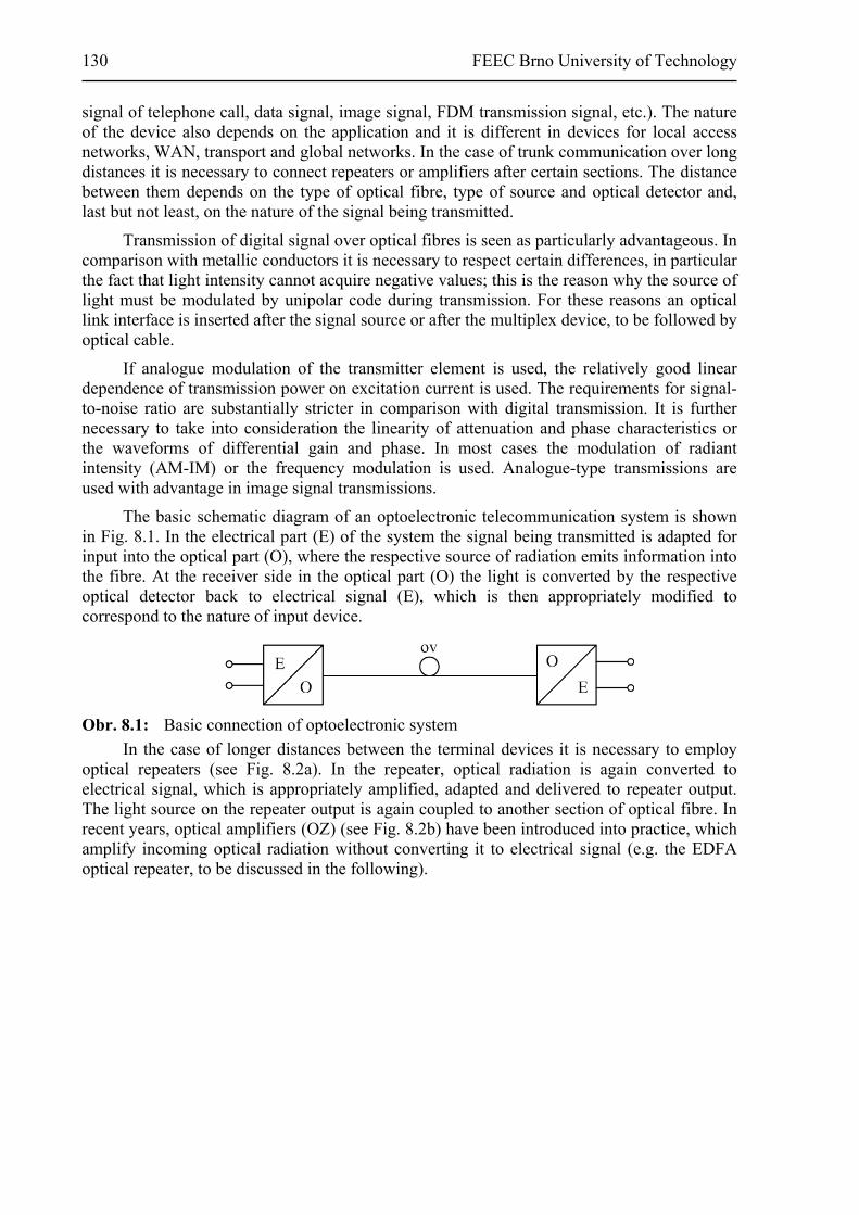
130 FEEC Brno University of Technology
signal of telephone call, data signal, image signal, FDM transmission signal, etc.). The nature of the device also depends on the application and it is different in devices for local access networks, WAN, transport and global networks. In the case of trunk communication over long distances it is necessary to connect repeaters or amplifiers after certain sections. The distance between them depends on the type of optical fibre, type of source and optical detector and, last but not least, on the nature of the signal being transmitted.
Transmission of digital signal over optical fibres is seen as particularly advantageous. In comparison with metallic conductors it is necessary to respect certain differences, in particular the fact that light intensity cannot acquire negative values; this is the reason why the source of light must be modulated by unipolar code during transmission. For these reasons an optical link interface is inserted after the signal source or after the multiplex device, to be followed by optical cable.
If analogue modulation of the transmitter element is used, the relatively good linear dependence of transmission power on excitation current is used. The requirements for signal-to-noise ratio are substantially stricter in comparison with digital transmission. It is further necessary to take into consideration the linearity of attenuation and phase characteristics or the waveforms of differential gain and phase. In most cases the modulation of radiant intensity (AM-IM) or the frequency modulation is used. Analogue-type transmissions are used with advantage in image signal transmissions.
The basic schematic diagram of an optoelectronic telecommunication system is shown in Fig. 8.1. In the electrical part (E) of the system the signal being transmitted is adapted for input into the optical part (O), where the respective source of radiation emits information into the fibre. At the receiver side in the optical part (O) the light is converted by the respective optical detector back to electrical signal (E), which is then appropriately modified to correspond to the nature of input device.
Obr. 8.1: Basic connection of optoelectronic system
In the case of longer distances between the terminal devices it is necessary to employ optical repeaters (see Fig. 8.2a). In the repeater, optical radiation is again converted to electrical signal, which is appropriately amplified, adapted and delivered to repeater output. The light source on the repeater output is again coupled to another section of optical fibre. In recent years, optical amplifiers (OZ) (see Fig. 8.2b) have been introduced into practice, which amplify incoming optical radiation without converting it to electrical signal (e.g. the EDFA optical repeater, to be discussed in the following).
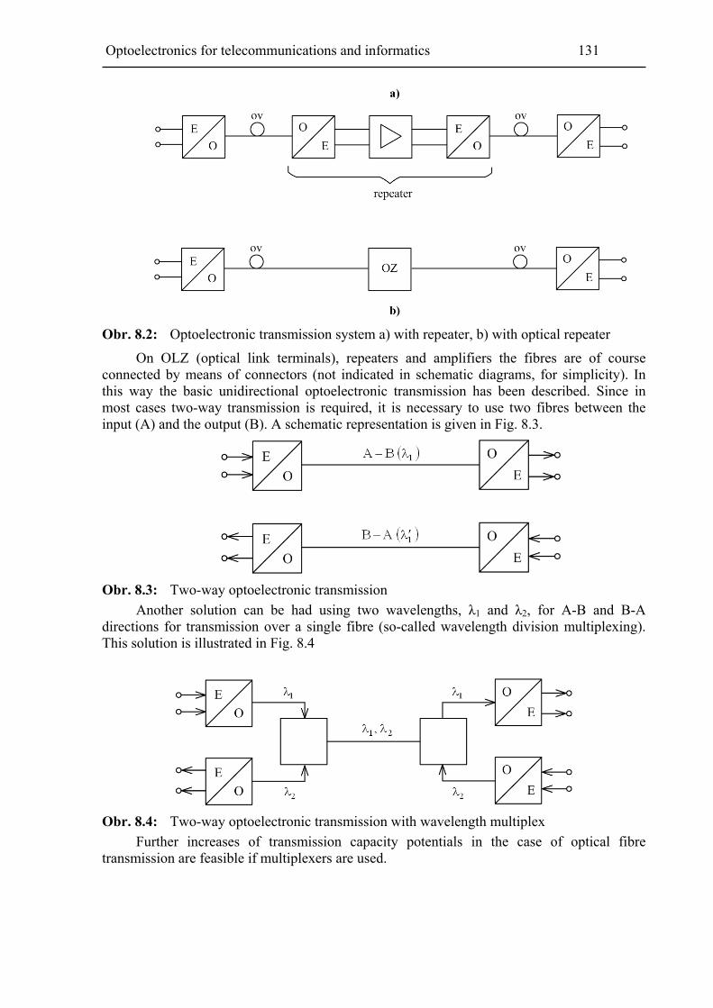
Optoelectronics for telecommunications and informatics 131
Obr. 8.2: Optoelectronic transmission system a) with repeater, b) with optical repeater
On OLZ (optical link terminals), repeaters and amplifiers the fibres are of course connected by means of connectors (not indicated in schematic diagrams, for simplicity). In this way the basic unidirectional optoelectronic transmission has been described. Since in most cases two-way transmission is required, it is necessary to use two fibres between the input (A) and the output (B). A schematic representation is given in Fig. 8.3.
Obr. 8.3: Two-way optoelectronic transmission
Another solution can be had using two wavelengths, λ1 and λ2, for A-B and B-A directions for transmission over a single fibre (so-called wavelength division multiplexing). This solution is illustrated in Fig. 8.4
Obr. 8.4: Two-way optoelectronic transmission with wavelength multiplex
Further increases of transmission capacity potentials in the case of optical fibre transmission are feasible if multiplexers are used.
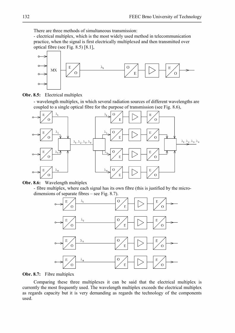
132 FEEC Brno University of Technology
There are three methods of simultaneous transmission: - electrical multiplex, which is the most widely used method in telecommunication practice, when the signal is first electrically multiplexed and then transmitted over optical fibre (see Fig. 8.5) [8.1],
Obr. 8.5: Electrical multiplex
- wavelength multiplex, in which several radiation sources of different wavelengths are coupled to a single optical fibre for the purpose of transmission (see Fig. 8.6),
Obr. 8.6: Wavelength multiplex
- fibre multiplex, where each signal has its own fibre (this is justified by the micro-dimensions of separate fibres – see Fig. 8.7).
Obr. 8.7: Fibre multiplex
Comparing these three multiplexes it can be said that the electrical multiplex is currently the most frequently used. The wavelength multiplex exceeds the electrical multiplex as regards capacity but it is very demanding as regards the technology of the components used.

Optoelectronics for telecommunications and informatics 133
The above examples form the basis of optoelectronic telecommunication systems. Systems that operate on their basis are higher-order digital systems, analogue systems, broadband systems (enabling both voice and video transmission), data transfer systems, etc. They are used not only in telecommunications but also in other sectors such as transport, automation, power engineering, etc.
In view of the application of these systems it is obvious that besides transmission parameters their reliability, supervision, location and error suppression must also be dealt with.
In the following sub-chapters we will be concerned with the basic problems of these systems and made familiar with some real systems.
8.1 Basic problems of optoelectronic systems
In this part we will outline some important problems concerning the reliable operation of optoelectronic systems. From a systems point of view, there are the following options in the design of a real device.
Type of signal being transmitted, from the viewpoint of the system: a) Digital - corresponding bit error rate, - bit rate. b) Analogue - corresponding width of transmitted band, - distortion. c) Radio - corresponding width of transmitted band, - distortion. d) Image - width of transmitted band - distortion.
In all the above cases it is necessary to consider the range of operating temperatures. Transmitter parameters: - input impedance, - maximum values of input signal, - radiation wavelength, - value of optical power, - corresponding power of supply source. Radiation source parameters: - radiation wavelength, - spectral bandwidth, - forward current, - overall optical power, - range of operating temperatures, - rise time and fall time. Fibre parameters: - type of fibre, - refractive index, - fibre attenuation, - numerical aperture,

134 FEEC Brno University of Technology
- distortion, - jacket and core diameters, - mechanical properties of fibre. Cable parameters: - number of fibres (groups), - diameter of fibre with coating, - cable diameter, - weight (in kilograms per kilometre), - minimum bend diameter. Detector parameters: - forward current, - operating wavelength, - output power, - range of operating temperatures, - rise time and fall time. Receiver parameters: - output impedance, - input level of signal, - optical sensitivity, - dynamic range, - rise time of output signal (analogue, digital), - corresponding power of supply source.
It is obvious from the above overview that when designing a system it is necessary to take into consideration many factors. In the first place, it is necessary to know the nature of information signal, i.e. digital or analogue signal. Another important factor is the route length, i.e. the distance between the transmitter and the receiver. Signal parameters need to be known too. What is a sufficient signal-to-noise ratio in the case of analogue signal? What is the bit error rate in digital signal? If the basic parameters are known, it is possible to proceed with the design of the system.
The design of an optoelectronic system is based on the following steps: - determination of the type of signal for information transmission, - definition of the bandwidth, - determination of the signal-to-noise ratio if analogue signal is used, - definition of the probability of error occurrence if analogue signal is used, - definition of the probability of error occurrence if digital signal is used (the minimum
value for digital transmission is PE = 10-9), - determination of transmission length, - selection of suitable optical fibre with respect to splice attenuation, - calculation of the fibre bandwidth for the system under consideration (the value is in
terms of MHz . km-1), - calculation of the power reserve (difference between output power and input
sensitivity of receiver), - determination of overall fibre attenuation with respect to length, - addition of losses on connectors, - addition of losses on splices, - reserve for temperature changes (1 dB), - reserve for time changes (2 dB), - the sum of the above attenuations gives the total system attenuation
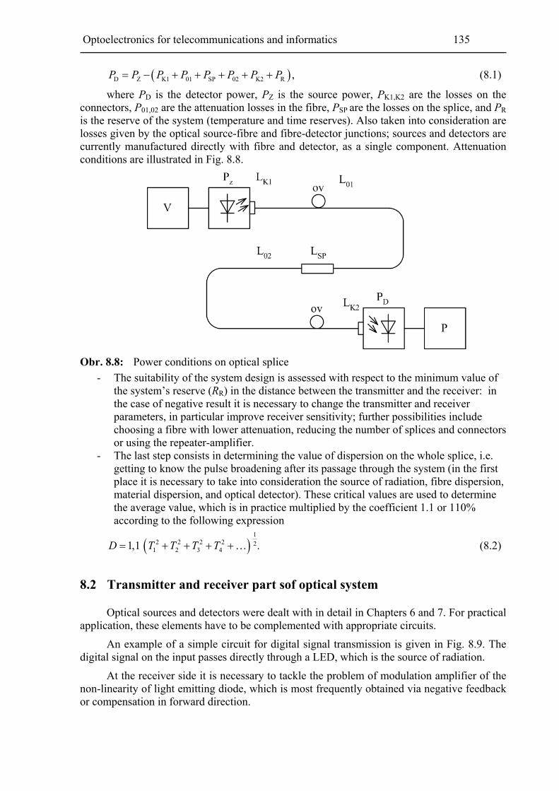
Optoelectronics for telecommunications and informatics 135
D Z K1 01 SP 02 K2 R ,P P P P P P P P (8.1)
where PD is the detector power, PZ is the source power, PK1,K2 are the losses on the connectors, P01,02 are the attenuation losses in the fibre, PSP are the losses on the splice, and PR is the reserve of the system (temperature and time reserves). Also taken into consideration are losses given by the optical source-fibre and fibre-detector junctions; sources and detectors are currently manufactured directly with fibre and detector, as a single component. Attenuation conditions are illustrated in Fig. 8.8.
Obr. 8.8: Power conditions on optical splice
- The suitability of the system design is assessed with respect to the minimum value of the system’s reserve (RR) in the distance between the transmitter and the receiver: in the case of negative result it is necessary to change the transmitter and receiver parameters, in particular improve receiver sensitivity; further possibilities include choosing a fibre with lower attenuation, reducing the number of splices and connectors or using the repeater-amplifier.
- The last step consists in determining the value of dispersion on the whole splice, i.e. getting to know the pulse broadening after its passage through the system (in the first place it is necessary to take into consideration the source of radiation, fibre dispersion, material dispersion, and optical detector). These critical values are used to determine the average value, which is in practice multiplied by the coefficient 1.1 or 110% according to the following expression
1
2 2 2 2 21 2 3 41,1 .D T T T T (8.2)
8.2 Transmitter and receiver part sof optical system
Optical sources and detectors were dealt with in detail in Chapters 6 and 7. For practical application, these elements have to be complemented with appropriate circuits.
An example of a simple circuit for digital signal transmission is given in Fig. 8.9. The digital signal on the input passes directly through a LED, which is the source of radiation.
At the receiver side it is necessary to tackle the problem of modulation amplifier of the non-linearity of light emitting diode, which is most frequently obtained via negative feedback or compensation in forward direction.
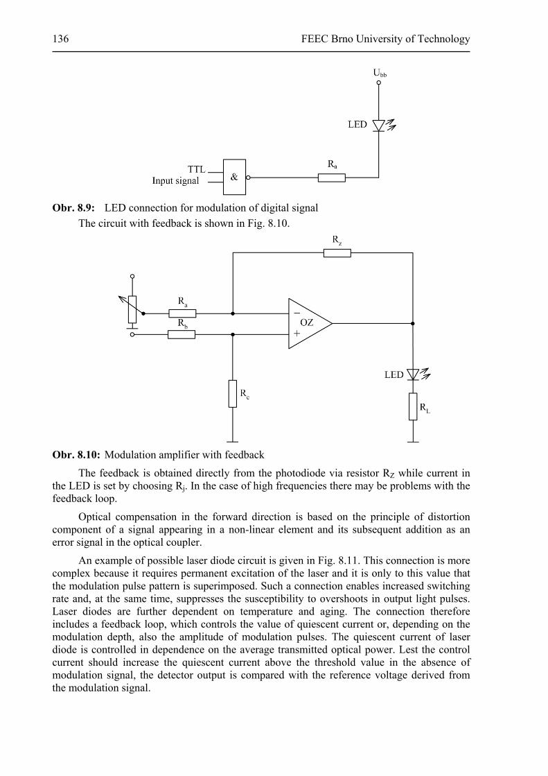
136 FEEC Brno University of Technology
Obr. 8.9: LED connection for modulation of digital signal
The circuit with feedback is shown in Fig. 8.10.
Obr. 8.10: Modulation amplifier with feedback
The feedback is obtained directly from the photodiode via resistor RZ while current in the LED is set by choosing Rj. In the case of high frequencies there may be problems with the feedback loop.
Optical compensation in the forward direction is based on the principle of distortion component of a signal appearing in a non-linear element and its subsequent addition as an error signal in the optical coupler.
An example of possible laser diode circuit is given in Fig. 8.11. This connection is more complex because it requires permanent excitation of the laser and it is only to this value that the modulation pulse pattern is superimposed. Such a connection enables increased switching rate and, at the same time, suppresses the susceptibility to overshoots in output light pulses. Laser diodes are further dependent on temperature and aging. The connection therefore includes a feedback loop, which controls the value of quiescent current or, depending on the modulation depth, also the amplitude of modulation pulses. The quiescent current of laser diode is controlled in dependence on the average transmitted optical power. Lest the control current should increase the quiescent current above the threshold value in the absence of modulation signal, the detector output is compared with the reference voltage derived from the modulation signal.
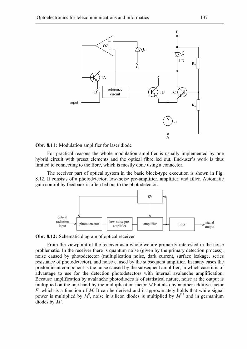
Optoelectronics for telecommunications and informatics 137
Obr. 8.11: Modulation amplifier for laser diode
For practical reasons the whole modulation amplifier is usually implemented by one hybrid circuit with preset elements and the optical fibre led out. End-user’s work is thus limited to connecting to the fibre, which is mostly done using a connector.
The receiver part of optical system in the basic block-type execution is shown in Fig. 8.12. It consists of a photodetector, low-noise pre-amplifier, amplifier, and filter. Automatic gain control by feedback is often led out to the photodetector.
Obr. 8.12: Schematic diagram of optical receiver
From the viewpoint of the receiver as a whole we are primarily interested in the noise problematic. In the receiver there is quantum noise (given by the primary detection process), noise caused by photodetector (multiplication noise, dark current, surface leakage, series resistance of photodetector), and noise caused by the subsequent amplifier. In many cases the predominant component is the noise caused by the subsequent amplifier, in which case it is of advantage to use for the detection photodetectors with internal avalanche amplification. Because amplification by avalanche photodiodes is of statistical nature, noise at the output is multiplied on the one hand by the multiplication factor M but also by another additive factor F, which is a function of M. It can be derived and it approximately holds that while signal power is multiplied by M2, noise in silicon diodes is multiplied by M2.3 and in germanium diodes by M3.

138 FEEC Brno University of Technology
Obr. 8.13: Equivalent diagram of input circuit of receiver
Equivalent diagram of the input circuit of optical signal receiver with direct detection is given in Fig. 8.13. It consists of a photodetector with internal amplification M and a load circuit. For the signal-to-noise ratio it holds
22
ts
2n ett b d
eq
12 ,
2 4
m I MP
Pq I I I M F M K f
R
(8.3)
where Ps/Pn is the ratio of signal power to noise power, m is the modulation index, M(ω) is the multiplication factor of photodiode, is is the photoelectric current (of both signal and background) (A), It is the current excited by signal (A), Ib is the current excited by background, Id is the photodetector dark current (A), Δf is the electrical bandwidth of detection system (s-1), F(M) is the factor of noise increase due to internal amplification process, Req is the equivalent resistance of photodetector and input circuit of amplifier (Ω), υet is the effective thermal noise, inclusive of thermal noise of detector, load resistance, and subsequent amplifier (K),
2vI is the average quadratic value of noise spike fIIIqI dbt
2v 2 ,
I2 is the effective value of the square of thermal noise fR
kI
eq
ef2 4 ,
q is the elementary charge 1,6 . 10-19C.
Relation (8.3) can be used to determine the minimum Ps/Pn ratio in dependence on the multiplication factor M, with which the noise spike caused by the average optical signal, background and dark current is multiplied to a level identical to the level of the thermal noise of subsequent amplifier. The calculation can also be made for photodiodes without internal amplification, in which case M = 1.
The Ps/Pn ratio is an important value in the design of optical system. In view of the absolute level of optical signal powers this ratio is a limiting factor from the viewpoint of the cut-off frequency of the system. This dependence is for the PIN photodetector shown in Fig. 8.14.

Optoelectronics for telecommunications and informatics 139
Obr. 8.14: Dependence of required average optical power at receiver input on frequency with Ps/Pn parameter for PIN photodiode
For the case when an avalanche photodiode is used as the detector, the dependence is shown in Fig. 8.15.
Obr. 8.15: Dependence of required average optical power at receiver input on frequency with Ps/Pn parameter for APD photodiode
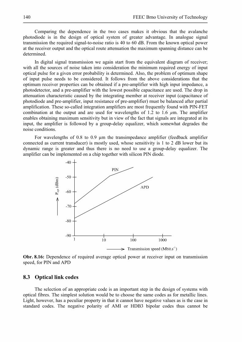
140 FEEC Brno University of Technology
Comparing the dependence in the two cases makes it obvious that the avalanche photodiode is in the design of optical system of greater advantage. In analogue signal transmission the required signal-to-noise ratio is 40 to 60 dB. From the known optical power at the receiver output and the optical route attenuation the maximum spanning distance can be determined.
In digital signal transmission we again start from the equivalent diagram of receiver; with all the sources of noise taken into consideration the minimum required energy of input optical pulse for a given error probability is determined. Also, the problem of optimum shape of input pulse needs to be considered. It follows from the above considerations that the optimum receiver properties can be obtained if a pre-amplifier with high input impedance, a photodetector, and a pre-amplifier with the lowest possible capacitance are used. The drop in attenuation characteristic caused by the integrating member at receiver input (capacitance of photodiode and pre-amplifier, input resistance of pre-amplifier) must be balanced after partial amplification. These so-called integration amplifiers are most frequently found with PIN-FET combination at the output and are used for wavelengths of 1.2 to 1.6 µm. The amplifier enables obtaining maximum sensitivity but in view of the fact that signals are integrated at its input, the amplifier is followed by a group-delay equalizer, which somewhat degrades the noise conditions.
For wavelengths of 0.8 to 0.9 µm the transimpedance amplifier (feedback amplifier connected as current transducer) is mostly used, whose sensitivity is 1 to 2 dB lower but its dynamic range is greater and thus there is no need to use a group-delay equalizer. The amplifier can be implemented on a chip together with silicon PIN diode.
Obr. 8.16: Dependence of required average optical power at receiver input on transmission speed, for PIN and APD
8.3 Optical link codes
The selection of an appropriate code is an important step in the design of systems with optical fibres. The simplest solution would be to choose the same codes as for metallic lines. Light, however, has a peculiar property in that it cannot have negative values as is the case in standard codes. The negative polarity of AMI or HDB3 bipolar codes thus cannot be

Optoelectronics for telecommunications and informatics 141
represented directly but in a round-about way: either by a ternary code with permanent bias voltage or by a unipolar code with information content higher than or equal to the ternary code. Another possibility is to convert bipolar signal to its equivalent binary form with subsequent transition to a suitable link code.
The selection itself and the design of code are part of the overall conception of the transmission system. The codes currently form a relatively large category so that proposing a new coding rule for a new system is practically out of the question. The following requirements are put on a link signal generated on the basis of a given rule [8-2]:
- high content of the clock cycle component, - constant dc component, - minimum bandwidth, - simple detection of bit error rate, - simple encoder and decoder circuitry, - system compatibility.
Because of the nature of optical transmission, there are additional requirements: power and linearity of the modulation characteristic of radiation source, attenuation and bandwidth of optical cable, sensitivity and noise conditions of radiation detector.
Because of their simplicity the NRZ (no return to zero) and RZ (return to zero) codes are frequently used. To eliminate the long sequence of zeros and ones an encoding and a decoding device is installed in the transmitter and receiver, where code rewriting takes place. Automatic measurement of the coefficient of bit error rate is performed via parity check sum.
Higher-order signals are transmitted using the mBnB codes, in which each word of the message being transmitted, m bits long, is recoded via a defined rule into an n-bit word(n > m).
For example, for second-order transmission systems type 1B2B link code has been chosen, which requires a two-fold transmission bandwidth but its solution of the encoder and decoder circuitry is relatively simple.
In the selection of the type of 1B2B code the following codes can be considered: CMI (Codec Mark Inversion), DMI (Differential Mark Inversion), MCMI (Modified CMI) and MDMI (Modified DMI). An example of the waveforms of link codes is given in Fig. 8.17.

142 FEEC Brno University of Technology
Obr. 8.17: Waveforms of link codes
It follows from the definition of codes that the CMI and DMI codes are assigned to the binary code while the MCMI and MDMI codes are assigned directly to the HDB3 code. On the basis of an analysis of the functional diagrams of code converters the application of the 1B2B code with direct assignment to HDB3 has been found advantageous. When choosing between the MCMI code and the MDMI code it is preferable to choose the MCMI code because the clock phase signal T is directly coupled to the trailing edge of MCMI signal (see Fig. 8.17).
The MCMI link code is used by many manufacturers (Siemens for example) in digital systems. A comparison of the normalized spectrum of MCMI code with other codes is given in Fig. 8.18, where P is the average power, and f = 1 . T-1 = 8448 kHz.
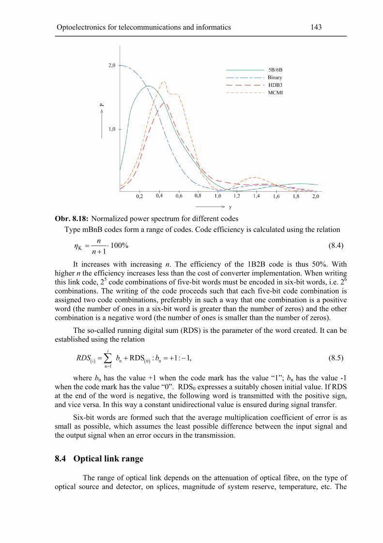
Optoelectronics for telecommunications and informatics 143
Obr. 8.18: Normalized power spectrum for different codes
Type mBnB codes form a range of codes. Code efficiency is calculated using the relation
%1001K
n
nη (8.4)
It increases with increasing n. The efficiency of the 1B2B code is thus 50%. With higher n the efficiency increases less than the cost of converter implementation. When writing this link code, 25 code combinations of five-bit words must be encoded in six-bit words, i.e. 26
combinations. The writing of the code proceeds such that each five-bit code combination is assigned two code combinations, preferably in such a way that one combination is a positive word (the number of ones in a six-bit word is greater than the number of zeros) and the other combination is a negative word (the number of ones is smaller than the number of zeros).
The so-called running digital sum (RDS) is the parameter of the word created. It can be established using the relation
n ni 0n 1
RDS : 1: 1,i
RDS b b
(8.5)
where bn has the value +1 when the code mark has the value “1”; bn has the value -1 when the code mark has the value “0”. RDS0 expresses a suitably chosen initial value. If RDS at the end of the word is negative, the following word is transmitted with the positive sign, and vice versa. In this way a constant unidirectional value is ensured during signal transfer.
Six-bit words are formed such that the average multiplication coefficient of error is as small as possible, which assumes the least possible difference between the input signal and the output signal when an error occurs in the transmission.
8.4 Optical link range
The range of optical link depends on the attenuation of optical fibre, on the type of optical source and detector, on splices, magnitude of system reserve, temperature, etc. The
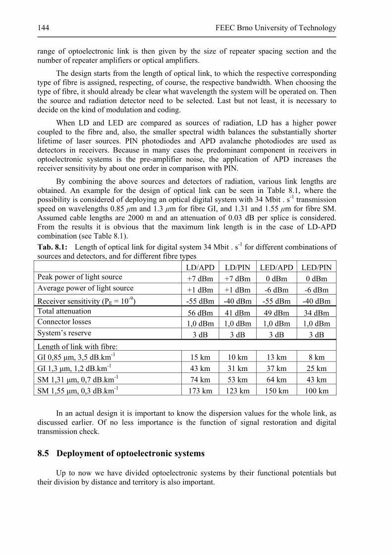
144 FEEC Brno University of Technology
range of optoelectronic link is then given by the size of repeater spacing section and the number of repeater amplifiers or optical amplifiers.
The design starts from the length of optical link, to which the respective corresponding type of fibre is assigned, respecting, of course, the respective bandwidth. When choosing the type of fibre, it should already be clear what wavelength the system will be operated on. Then the source and radiation detector need to be selected. Last but not least, it is necessary to decide on the kind of modulation and coding.
When LD and LED are compared as sources of radiation, LD has a higher power coupled to the fibre and, also, the smaller spectral width balances the substantially shorter lifetime of laser sources. PIN photodiodes and APD avalanche photodiodes are used as detectors in receivers. Because in many cases the predominant component in receivers in optoelectronic systems is the pre-amplifier noise, the application of APD increases the receiver sensitivity by about one order in comparison with PIN.
By combining the above sources and detectors of radiation, various link lengths are obtained. An example for the design of optical link can be seen in Table 8.1, where the possibility is considered of deploying an optical digital system with 34 Mbit . s-1 transmission speed on wavelengths 0.85 μm and 1.3 μm for fibre GI, and 1.31 and 1.55 μm for fibre SM. Assumed cable lengths are 2000 m and an attenuation of 0.03 dB per splice is considered. From the results it is obvious that the maximum link length is in the case of LD-APD combination (see Table 8.1).
Tab. 8.1: Length of optical link for digital system 34 Mbit . s-1 for different combinations of sources and detectors, and for different fibre types
LD/APD LD/PIN LED/APD LED/PINPeak power of light source +7 dBm +7 dBm 0 dBm 0 dBmAverage power of light source +1 dBm +1 dBm -6 dBm -6 dBm
Receiver sensitivity (PE = 10-9) -55 dBm -40 dBm -55 dBm -40 dBmTotal attenuation 56 dBm 41 dBm 49 dBm 34 dBmConnector losses 1,0 dBm 1,0 dBm 1,0 dBm 1,0 dBmSystem’s reserve 3 dB 3 dB 3 dB 3 dB
Length of link with fibre:GI 0,85 μm, 3,5 dB.km-1 15 km 10 km 13 km 8 km
GI 1,3 μm, 1,2 dB.km-1 43 km 31 km 37 km 25 km
SM 1,31 μm, 0,7 dB.km-1 74 km 53 km 64 km 43 km
SM 1,55 μm, 0,3 dB.km-1 173 km 123 km 150 km 100 km
In an actual design it is important to know the dispersion values for the whole link, as discussed earlier. Of no less importance is the function of signal restoration and digital transmission check.
8.5 Deployment of optoelectronic systems
Up to now we have divided optoelectronic systems by their functional potentials but their division by distance and territory is also important.
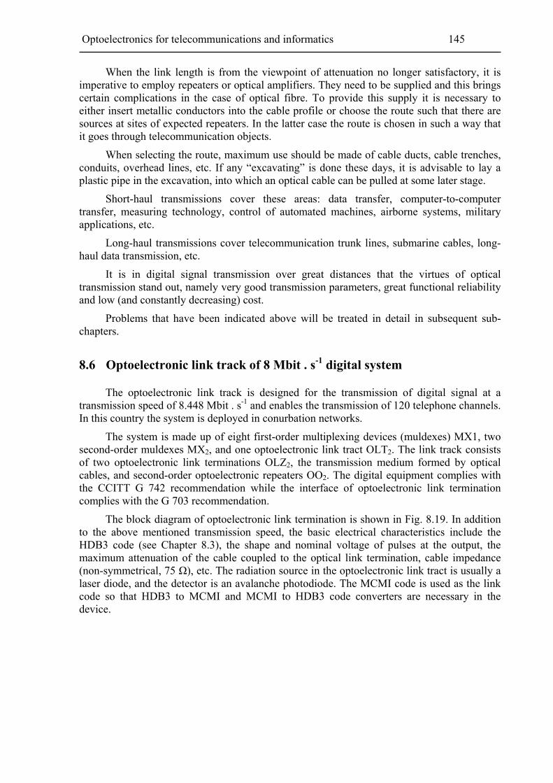
Optoelectronics for telecommunications and informatics 145
When the link length is from the viewpoint of attenuation no longer satisfactory, it is imperative to employ repeaters or optical amplifiers. They need to be supplied and this brings certain complications in the case of optical fibre. To provide this supply it is necessary to either insert metallic conductors into the cable profile or choose the route such that there are sources at sites of expected repeaters. In the latter case the route is chosen in such a way that it goes through telecommunication objects.
When selecting the route, maximum use should be made of cable ducts, cable trenches, conduits, overhead lines, etc. If any “excavating” is done these days, it is advisable to lay a plastic pipe in the excavation, into which an optical cable can be pulled at some later stage.
Short-haul transmissions cover these areas: data transfer, computer-to-computer transfer, measuring technology, control of automated machines, airborne systems, military applications, etc.
Long-haul transmissions cover telecommunication trunk lines, submarine cables, long-haul data transmission, etc.
It is in digital signal transmission over great distances that the virtues of optical transmission stand out, namely very good transmission parameters, great functional reliability and low (and constantly decreasing) cost.
Problems that have been indicated above will be treated in detail in subsequent sub-chapters.
8.6 Optoelectronic link track of 8 Mbit . s-1 digital system
The optoelectronic link track is designed for the transmission of digital signal at a transmission speed of 8.448 Mbit . s-1 and enables the transmission of 120 telephone channels. In this country the system is deployed in conurbation networks.
The system is made up of eight first-order multiplexing devices (muldexes) MX1, two second-order muldexes MX2, and one optoelectronic link tract OLT2. The link track consists of two optoelectronic link terminations OLZ2, the transmission medium formed by optical cables, and second-order optoelectronic repeaters OO2. The digital equipment complies with the CCITT G 742 recommendation while the interface of optoelectronic link termination complies with the G 703 recommendation.
The block diagram of optoelectronic link termination is shown in Fig. 8.19. In addition to the above mentioned transmission speed, the basic electrical characteristics include the HDB3 code (see Chapter 8.3), the shape and nominal voltage of pulses at the output, the maximum attenuation of the cable coupled to the optical link termination, cable impedance (non-symmetrical, 75 Ω), etc. The radiation source in the optoelectronic link tract is usually a laser diode, and the detector is an avalanche photodiode. The MCMI code is used as the link code so that HDB3 to MCMI and MCMI to HDB3 code converters are necessary in the device.
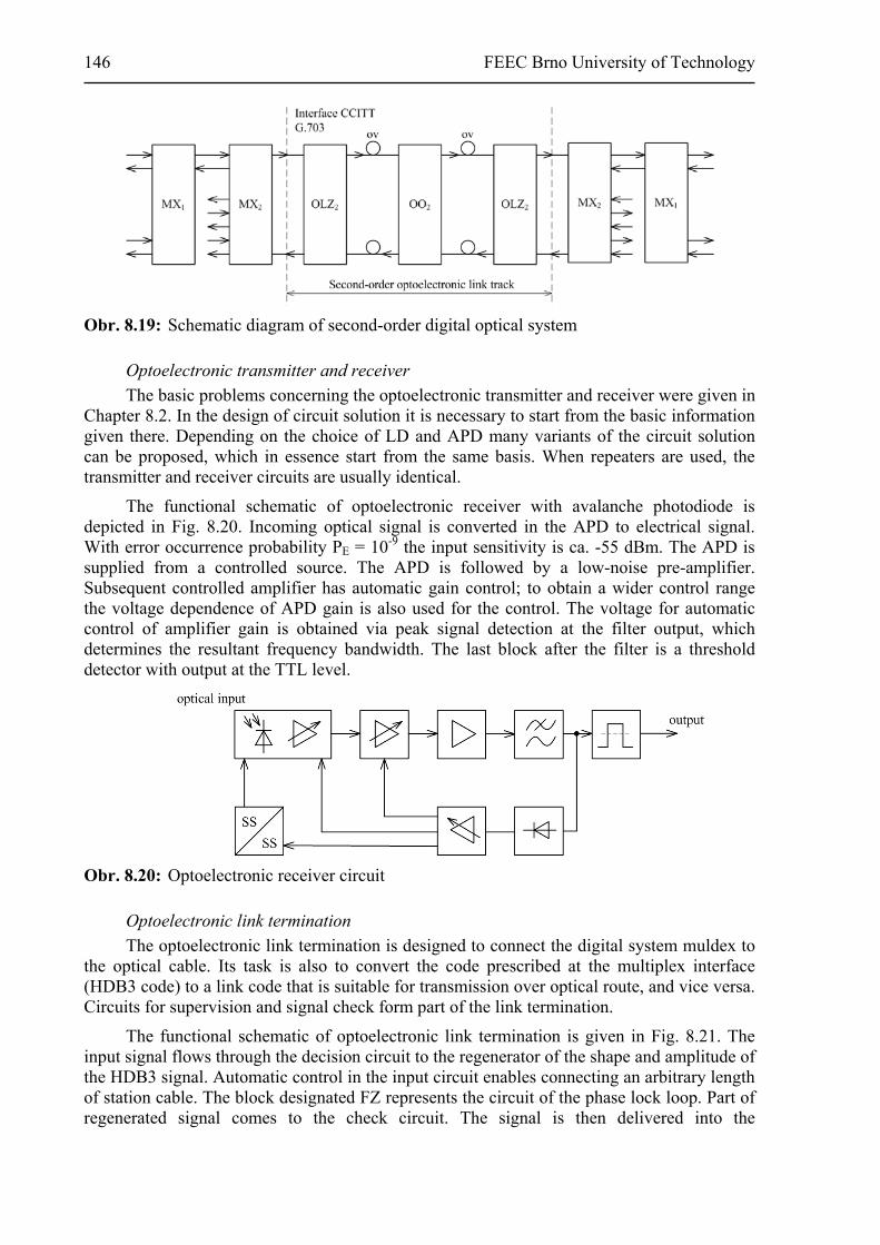
146 FEEC Brno University of Technology
Obr. 8.19: Schematic diagram of second-order digital optical system
Optoelectronic transmitter and receiver
The basic problems concerning the optoelectronic transmitter and receiver were given in Chapter 8.2. In the design of circuit solution it is necessary to start from the basic information given there. Depending on the choice of LD and APD many variants of the circuit solution can be proposed, which in essence start from the same basis. When repeaters are used, the transmitter and receiver circuits are usually identical.
The functional schematic of optoelectronic receiver with avalanche photodiode is depicted in Fig. 8.20. Incoming optical signal is converted in the APD to electrical signal. With error occurrence probability PE = 10-9 the input sensitivity is ca. -55 dBm. The APD is supplied from a controlled source. The APD is followed by a low-noise pre-amplifier. Subsequent controlled amplifier has automatic gain control; to obtain a wider control range the voltage dependence of APD gain is also used for the control. The voltage for automatic control of amplifier gain is obtained via peak signal detection at the filter output, which determines the resultant frequency bandwidth. The last block after the filter is a threshold detector with output at the TTL level.
Obr. 8.20: Optoelectronic receiver circuit
Optoelectronic link termination
The optoelectronic link termination is designed to connect the digital system muldex to the optical cable. Its task is also to convert the code prescribed at the multiplex interface (HDB3 code) to a link code that is suitable for transmission over optical route, and vice versa. Circuits for supervision and signal check form part of the link termination.
The functional schematic of optoelectronic link termination is given in Fig. 8.21. The input signal flows through the decision circuit to the regenerator of the shape and amplitude of the HDB3 signal. Automatic control in the input circuit enables connecting an arbitrary length of station cable. The block designated FZ represents the circuit of the phase lock loop. Part of regenerated signal comes to the check circuit. The signal is then delivered into the
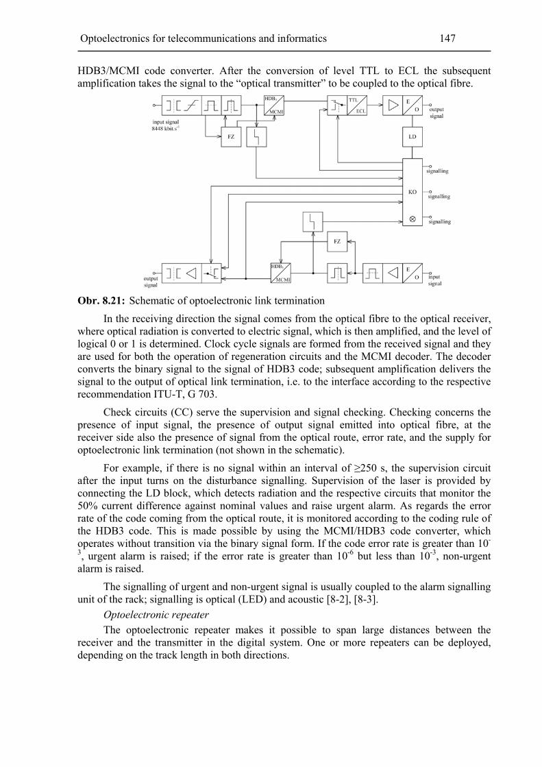
Optoelectronics for telecommunications and informatics 147
HDB3/MCMI code converter. After the conversion of level TTL to ECL the subsequent amplification takes the signal to the “optical transmitter” to be coupled to the optical fibre.
Obr. 8.21: Schematic of optoelectronic link termination
In the receiving direction the signal comes from the optical fibre to the optical receiver, where optical radiation is converted to electric signal, which is then amplified, and the level of logical 0 or 1 is determined. Clock cycle signals are formed from the received signal and they are used for both the operation of regeneration circuits and the MCMI decoder. The decoder converts the binary signal to the signal of HDB3 code; subsequent amplification delivers the signal to the output of optical link termination, i.e. to the interface according to the respective recommendation ITU-T, G 703.
Check circuits (CC) serve the supervision and signal checking. Checking concerns the presence of input signal, the presence of output signal emitted into optical fibre, at the receiver side also the presence of signal from the optical route, error rate, and the supply for optoelectronic link termination (not shown in the schematic).
For example, if there is no signal within an interval of ≥250 s, the supervision circuit after the input turns on the disturbance signalling. Supervision of the laser is provided by connecting the LD block, which detects radiation and the respective circuits that monitor the 50% current difference against nominal values and raise urgent alarm. As regards the error rate of the code coming from the optical route, it is monitored according to the coding rule of the HDB3 code. This is made possible by using the MCMI/HDB3 code converter, which operates without transition via the binary signal form. If the code error rate is greater than 10-
3, urgent alarm is raised; if the error rate is greater than 10-6 but less than 10-3, non-urgent alarm is raised.
The signalling of urgent and non-urgent signal is usually coupled to the alarm signalling unit of the rack; signalling is optical (LED) and acoustic [8-2], [8-3].
Optoelectronic repeater
The optoelectronic repeater makes it possible to span large distances between the receiver and the transmitter in the digital system. One or more repeaters can be deployed, depending on the track length in both directions.

148 FEEC Brno University of Technology
The functional schematic of repeater is given in Fig. 8.22. Here the input optical signal is converted to electric signal, amplified and regenerated. Then it is prepared for conversion to optical signal (the same circuits as in the optical link termination).
Repeater operation needs supply. Supply is either from a local source or by means of metallic conductors, which are attached in the cable core together with optical fibres. An example of the supply for the repeater and also remote supervision of the repeater is illustrated in Fig. 8.22. Using a metallic line, the laser output is signaled and checked and the repeater input is also checked, inclusive of the rate of error occurrence. In the repeater the MCMI code is again converted to the HDB3 code, which then initiates the respective circuits; after amplification and transmission over the metallic line it is evaluated as an alarm signal in the respective terminal station.
New elements, so-called optical amplifiers, have recently come to be applied in optical transmissions; they do not require the O/E and reverse E/O signal conversion. These are universal elements. They will be dealt with in greater detail in Chapter 8.16.
Obr. 8.22: Schematic of optoelectronic repeater with remote supervision
8.7 Optoelectronic link track of 34 Mbit . s-1 digital system
The digital optoelectronic track is designed for two-way transmission of digital signals at a transmission speed of 34.368 Mbit . s-1 along two optical fibres. It is part of a third-order digital transmission system, which enables the transmission of 480 telephone channels, as well as transfer of data, radio modulation, and TV signal.
The optoelectronic track is formed by two third-order optoelectronic link terminations, optical medium, and, depending on the link length, repeaters. At each end the whole system is composed of 16 first-order multiplex devices, 4 second-order multiplex devices, and one third-order multiplex device.
The code prescribed for digital systems is HDB3 with a transmission speed of 34.368 Mbit . s-1. The functional and electrical parameters of contact circuits for multiplex interface are defined in the ITU-T G.703 and G.823 recommendations.
Again, the optical transmitter and receiver are part of the link termination. The design of the termination is usually such that optoelectronic converters (LD, LED, APD, and PIN) and various transmission wavelengths can be changed easily.
Optoelectronic link termination
The functional schematic of the transmitter and receiver of optoelectronic link termination is given in Fig. 8.23.

Optoelectronics for telecommunications and informatics 149
Obr. 8.23: Schematic of third-order optoelectronic link termination
The input signal (from the multiplex device) is delivered into the regenerative circuits of the HDB3 block, where the signal is first processed in an automatic corrector. Its task is to remove the frequency-dependent attenuation of the connecting cable between the multiplex device and the optoelectronic link termination and to obtain in the decision circuit a pulse shape that is optimum from the viewpoint of resistance to disturbance and symbol interference.
The signal is then converted to unipolar signal suitable for optical transmission and conducted via a scrambler to the HDB3/5B6B code converter.
The task of the scrambler is to convert the non-uniformly distributed ones and zeros of the binary block to pseudorandom signals with more or less uniform temporal distribution of energy. In the HDB3/5B6B coder the input signal is first converted in the HDB3/NRZ converter to NRZ code according to the coding algorithm.
The practical implementation of the NRZ/5B6B code converter is such that the signal encoded in NRZ is first delivered to a series/parallel converter. Five-bit parallel-arranged words come from the converter output to the addresses of PROM memory, where the conversion itself of five-bit words to six-bit words takes place. A parallel/series converter is inserted at the PROM memory output, which provides for the conversion of the six-bit word back to the series form.
Via the next block of the optical transmitter, information in the form of radiation is transmitted into the optical fibre. Time-base circuits, check circuits (CC), supervision circuits, supply circuits, etc. form part of the transmitter of optoelectronic link termination.
In the receiver the optical signal is converted back to an electrical signal, which is conducted to the amplifier whose gain can be controlled by the voltage of automatic sensitivity balance. In dependence on the optical power at the receiver input the gain is changed such that the level of output signal of optoelectronic receiver remains almost constant. The signal is then conveyed to a low-pass filter, which corrects the frequency response of optical receiver to an optimum from the viewpoint of symbol interference of output pulses. At the output of optical receiver we again obtain a unipolar signal encoded in 5B6B, at a level of 1 V and 75 Ω load, which characterizes the internal interface of the optoelectronic and electrical part of receiver.
The task of the next block of 5B6B code regeneration is the time, shape and amplitude regeneration of the signal of this code. The presence or absence of the signal is evaluated in the check circuit.

150 FEEC Brno University of Technology
Analogously to the transmission side, the last three blocks are blocks that ensure decoding, i.e. the conversion of the 5B6B code, via descrambler, to the HDB3 code, which is required for the defined interface.
8.8 Optoelectronic linhk track of 140 Mbit . s-1 digital system
The optoelectronic link track is designed for the 140 Mbit . s-1 transmission speed, with transmission over gradient-index fibre or single-mode fibre, operating most frequently on the 1.31 μm wavelength. In the design it is essentially an analogy to the preceding solution.
Using the LD source and type GI fibre, repeater spacing of almost 30 km can be obtained; with the SI fibre the utmost limit is about 120 km.
Again in compliance with the ITU-T recommendations, the incoming input signal from the electrical interface, encoded in CMI, is corrected for transmission over optical fibre. For this reason the input signal is processed in the automatic corrector, regenerated, decoded, and conveyed to the scrambler. Then it is converted to the 5B6B binary link code. In the optoelectronic transmitter block the electrical signal is transformed into optical signal.
8.9 Optoelectronic link track of 565 Mbit . s-1 digital system
Digital systems of the fifth order markedly enhance the economic aspect of information transmission but at the cost of more demanding requirements placed on the technical level of devices. These systems are suitable for long transport routes. Their transmission speed is 565 Mbit . s-1, they are deployed on single-mode fibres, and they use the operating region of the 1.31 μm and 1.55 μm wavelengths. In essence, they are a multiplex of 4 systems of 140 Mbit . s-1 transmission speed using the time or wavelength division multiplex. The application of single-mode fibre puts increased demands on coupling the radiation to the fibre, on connectors, splices, etc. On the other hand, the high transmission speed places high demands on the optical transmitter, which must generate pulses of extremely narrow spectral width.
The functional schematic of the system is given in Fig. 8.24. The multiplexer (MUX) mentioned earlier combines 4 x 140 Mbit . s-1 systems; the remaining blocks are basically identical to the third-order system described above. The difference is only in the design of circuitry, which must provide higher transmission speeds. The application of scrambler (descrambler) is mostly limited and integrated to 140 Mbit . s-1. Synchronization is performed via phase lock. Supply, signalling and supervision circuits also form part of the optoelectronic link termination.

Optoelectronics for telecommunications and informatics 151
Obr. 8.24: Schematic of fifth-order optoelectronic link termination
The 565 Mbit . s-1 transmission speed corresponds to 7680 telephone channels or eight colour TV channels.
Similar circuits for optical interface – OLT “plate” (optical link termination) are implemented for SDH systems, specifically for STM-1 with 0.155 Gbit . s-1 transmission speed, STM-4 with 0.622 Gbit . s-1 transmission speed, STM-16 with 2.5 Gbit . s-1 transmission speed, possibly also STM-64 and STM-256 with 10 and 40 Gbit . s-1 transmission speeds, respectively.
The design of OLT will, of course, be different from different manufacturers but at the inputs and outputs they must respect the relevant ITU standards. The dominant parameters are distortion and error rate, above all in dependence on the required higher transmission speeds.
Further increases in the transmission capacity of fibres in the order of tens of Gbit. s-1 or more are implemented on the principles of wavelength multiplexes (see Chapter 8.16).
8.10 Optoelectronic systems for transmission of analogue modulation
Current world trends in the digitization of telecommunication networks give strong preference to the transmission of digital signals over optical fibres but even so the transmission of analogue signals has and will have its justification. In some respects the transmission of analogue signal over fibre is problematic while in the case of TV signal transmission its advantageous features stand out.
Problems appearing in the transmission of analogue signals arise from the non-linearity of elements. Under regular conditions in optical fibre with non-linear properties they need not be taken into consideration. Problems only begin to appear at higher powers. The case of detectors is in this respect similar. The main problem consists in the output characteristics of semiconductor sources of radiation. From the viewpoint of these transmissions it is imperative to linearize the operating part of the characteristic.
The most frequently used modulations are the direct intensity modulation IM and the pulse frequency modulation PFM – IM.
The IM method is suitable when power superluminescence diodes are used, which have a relatively good linear characteristic for less demanding applications, for example short-haul links. For more demanding links (greater distance, higher frequency, TV signal) the
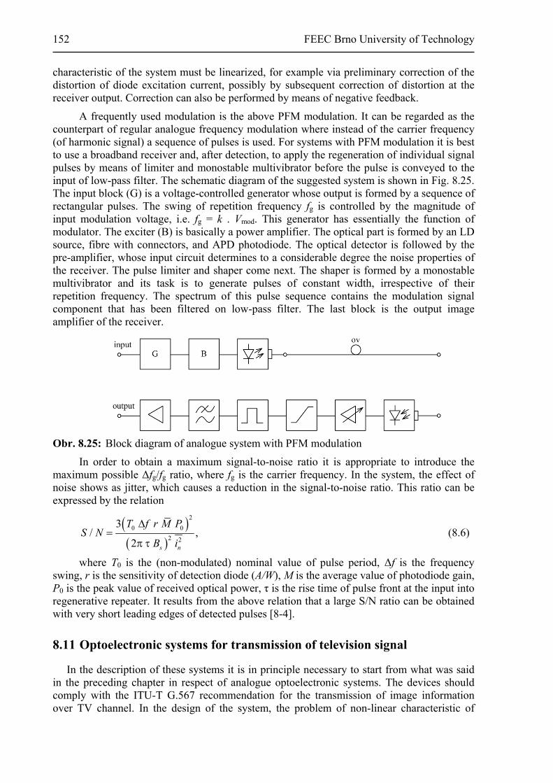
152 FEEC Brno University of Technology
characteristic of the system must be linearized, for example via preliminary correction of the distortion of diode excitation current, possibly by subsequent correction of distortion at the receiver output. Correction can also be performed by means of negative feedback.
A frequently used modulation is the above PFM modulation. It can be regarded as the counterpart of regular analogue frequency modulation where instead of the carrier frequency (of harmonic signal) a sequence of pulses is used. For systems with PFM modulation it is best to use a broadband receiver and, after detection, to apply the regeneration of individual signal pulses by means of limiter and monostable multivibrator before the pulse is conveyed to the input of low-pass filter. The schematic diagram of the suggested system is shown in Fig. 8.25. The input block (G) is a voltage-controlled generator whose output is formed by a sequence of rectangular pulses. The swing of repetition frequency fg is controlled by the magnitude of input modulation voltage, i.e. fg = k . Vmod. This generator has essentially the function of modulator. The exciter (B) is basically a power amplifier. The optical part is formed by an LD source, fibre with connectors, and APD photodiode. The optical detector is followed by the pre-amplifier, whose input circuit determines to a considerable degree the noise properties of the receiver. The pulse limiter and shaper come next. The shaper is formed by a monostable multivibrator and its task is to generate pulses of constant width, irrespective of their repetition frequency. The spectrum of this pulse sequence contains the modulation signal component that has been filtered on low-pass filter. The last block is the output image amplifier of the receiver.
Obr. 8.25: Block diagram of analogue system with PFM modulation
In order to obtain a maximum signal-to-noise ratio it is appropriate to introduce the maximum possible Δfg/fg ratio, where fg is the carrier frequency. In the system, the effect of noise shows as jitter, which causes a reduction in the signal-to-noise ratio. This ratio can be expressed by the relation
2
0 0
2 2
3/ ,
2 s n
T f r M PS N
B i
(8.6)
where T0 is the (non-modulated) nominal value of pulse period, Δf is the frequency swing, r is the sensitivity of detection diode (A/W), M is the average value of photodiode gain, P0 is the peak value of received optical power, τ is the rise time of pulse front at the input into regenerative repeater. It results from the above relation that a large S/N ratio can be obtained with very short leading edges of detected pulses [8-4].
8.11 Optoelectronic systems for transmission of television signal
In the description of these systems it is in principle necessary to start from what was said in the preceding chapter in respect of analogue optoelectronic systems. The devices should comply with the ITU-T G.567 recommendation for the transmission of image information over TV channel. In the design of the system, the problem of non-linear characteristic of

Optoelectronics for telecommunications and informatics 153
optical source comes again into the foreground. Direct intensity modulation cannot be adopted because this non-linearity is not adapted to the non-linear channel. The image signal is therefore first converted (modulated) to the 70 MHz frequency, which is then used to modulate the optical transmitter. To put it more precisely, the basic image signal band of 0 to 6 MHz is modulated to an intermediate frequency of 70 ± 4 MHz, and vice versa. It is only now that the transmitting optical element in the receiver block can be modulated by intensity modulation. For these purposes the GI fibre of 0.85 μm wavelength is used most frequently. An example of the system, its functional connection, is shown in Fig. 8.26.
Obr. 8.26: Functional schematic of TV signal transmission over optical fibre
At the receiver side, the optical radiation is converted back to intermediate frequency, which is then converted to the basic band in the demodulator. For the image signal transmission the signal quality is defined according to the S/N ratio at the receiver output according to the relation
2
2tep
2/ ,
2e
m P r aS N
P r B i
(8.7)
where 2tepi is the average value of thermal noise current, P is the average value of
received optical power, m is the modulation index (ca. 0.8), r is the diode response (0.5 A/W for the PIN diode), a is the ratio of the brightness component of image signal to the total TV signal (0.7), and B is the receiver noise bandwidth (typically 5 – 6 MHz). From the practical viewpoint good results for the S/N ratio are obtained with input power into receiver P2 = 0.2 – 0.3 W. Transmitted optical power P1 = 1 mW can be considered. If connector losses of 1 dB and a system reserve of 6 dB are considered, an optical fibre attenuation of 28 dB can be considered, to which a distance of 7 km between transmitter and receiver would correspond in the case of GI fibre. The radiation source used is laser. If single-mode fibres are used, the spanning distance is increased.
8.12 Optoelectronic transmission systems for short distances
These systems are designed for (from the viewpoint of bandwidth and transmission speed) less demanding transmissions, in particular in local networks. The aim has been to design universal devices for the transmission of both analogue and digital signals, up t a transmission rate of 2 or 8 Mbit . s-1, possibly also digital telephone transmission for four subscribers.
8.13 Optoelectronic systems for industrial applications
These systems are also designed for transmission over short distances. They make full use of the advantages of transmission via optical radiation and are designed for data (signal) transmission in computer and automation technologies, transport, and at sites with a high level of electromagnetic interference (high-voltage switching stations), etc.
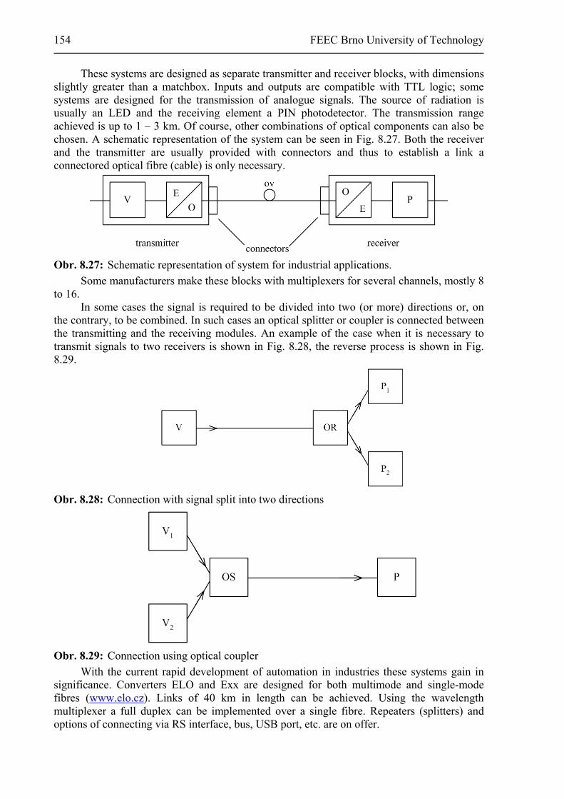
154 FEEC Brno University of Technology
These systems are designed as separate transmitter and receiver blocks, with dimensions slightly greater than a matchbox. Inputs and outputs are compatible with TTL logic; some systems are designed for the transmission of analogue signals. The source of radiation is usually an LED and the receiving element a PIN photodetector. The transmission range achieved is up to 1 – 3 km. Of course, other combinations of optical components can also be chosen. A schematic representation of the system can be seen in Fig. 8.27. Both the receiver and the transmitter are usually provided with connectors and thus to establish a link a connectored optical fibre (cable) is only necessary.
Obr. 8.27: Schematic representation of system for industrial applications.
Some manufacturers make these blocks with multiplexers for several channels, mostly 8 to 16. In some cases the signal is required to be divided into two (or more) directions or, on the contrary, to be combined. In such cases an optical splitter or coupler is connected between the transmitting and the receiving modules. An example of the case when it is necessary to transmit signals to two receivers is shown in Fig. 8.28, the reverse process is shown in Fig. 8.29.
Obr. 8.28: Connection with signal split into two directions
Obr. 8.29: Connection using optical coupler
With the current rapid development of automation in industries these systems gain in significance. Converters ELO and Exx are designed for both multimode and single-mode fibres (www.elo.cz). Links of 40 km in length can be achieved. Using the wavelength multiplexer a full duplex can be implemented over a single fibre. Repeaters (splitters) and options of connecting via RS interface, bus, USB port, etc. are on offer.
Optoelectronics for telecommunications and informatics 155
8.14 Local optical networks
Historically, the local optical network (LON) has evolved from the local area network (LAN), with the metallic transmission medium being replaced by optical fibre. Although the nature of the network does not change, there are certain differences, both advantages and drawbacks, inherent in optical transmission.
The local network as such refers to a transmission or communication system that guarantees data transmission among a theoretically infinite number of stations over a common transmission medium, and the whole of which is installed on the premises of a single user. These networks are mostly installed in industrial enterprises, schools, business companies, etc.
In comparison with metallic lines used in LAN (coaxial cables or shielded pair) the optical fibre offers higher transmission speeds, larger bandwidth, perfect resistance to electromagnetic interference, and galvanic separation of inputs and outputs. A disadvantage can be seen in the difficult splicing and in large optical power losses in directional couplers.
The local network can be characterized by the following basic criteria: - transmission medium, - transmission speed, - network topology, - method of user access to the network, - architecture. Transmission medium Most frequently, multimode media of larger core diameter and larger numerical aperture
are used. This choice will yield high-quality fixed and demountable fibre splices, easy handling, and effective coupling of radiant energy from radiation sources to the fibre. On the other hand, all this is at the expense of the attenuation values and bandwidth of such fibres. The dimensions of frequently used fibres are 50/125 µm, 62.5/125 µm, 100/140 µm, and others. In some cases single-mode fibres are also used, in particular for larger distances and higher transmission speeds.
Transmission speed According to transmission speed, local networks are divided into three groups:
- up to 10 Mbit . s-1 (low-speed networks), - up to 100 Mbit . s-1 (medium-speed networks), - over 100 Mbit . s-1 (high-speed networks).
In low-speed networks the application of optical fibres cannot be seen as most advantageous, unless a medium with strong electromagnetic field is concerned or perfect galvanic separation of both ends is required. An important LON requirement is a low price of transmission facilities. For this reason the 850 nm operating wavelength is mostly used, with LED diodes as radiation sources and PIN diodes as receivers.
In medium-speed networks and, in particular, high-speed networks the pros of optical transmission become significant. It should be noted that maximum transmission speed is not identical to information throughput of the network. The actual values mainly depend on the network access methods and usually they are about 70% of the transmission speed given. With higher transmission speeds the integration of data, video, voice, and services can be taken into consideration.

156 FEEC Brno University of Technology
Network topology The fundamental question of network topology is the connection of the terminal (station). In the case of metallic conductors, high-impedance connection of terminals is possible, but this connection cannot be implemented optically because it results in extremely high power losses in the directional coupler. An example of passive connection to the terminal is shown in Fig. 8.30a. In the case of connecting several terminals it is necessary to use active connection, which is in essence formed by a repeater with connected terminal (see Fig. 8.30b).
Obr. 8.30: Terminal connection a) passive, b) active
For small LON the passive star topology can be used. The principle is clear from Fig. 8.31. The active star topology can be implemented on a similar principle.
Obr. 8.31: Passive star topology
The ring topology is frequently used with advantage in LON. Examples of the passive and the active rings are given in Figs 8.32 and 8.33, respectively. From the viewpoint of secure transmission it is of advantage to use ring topology with two fibres. The connection of terminal device to such a network is shown in Fig. 8.34. When there is a failure in the first fibre, operation is re-directed to the second, backup, fibre. In the case of fibre outage between terminals fibre looping (dashed line) is performed on neighbouring terminals and operation may continue without break. The optical relay in the figure provides for “bypassing” the terminal, be it for passivity reason or in the case of failure.
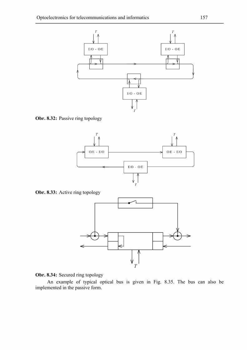
Optoelectronics for telecommunications and informatics 157
Obr. 8.32: Passive ring topology
Obr. 8.33: Active ring topology
Obr. 8.34: Secured ring topology
An example of typical optical bus is given in Fig. 8.35. The bus can also be implemented in the passive form.

158 FEEC Brno University of Technology
Obr. 8.35: Bus topology
So-called mixed topologies, implemented from passive and active topologies, are often used.
So-called hybrid topologies in local networks take advantage of metallic conductors for lower transmission speeds and lower network levels (buses) while for higher levels and higher transmission speeds they use optical fibres (ring topology). An example of this topology is given in Fig. 8.36.
Obr. 8.36: Hybrid topology
In the design of topologies it is of advantage to give preference to the wavelength division multiplexer.
LAN are used with advantage in administrative buildings, institutes, schools, etc., where mixed and hybrid topologies find application, most frequently of the star-ring or star-bus type.
Network reliability is then one of the most important parameters.
Access methods
The term medium access control (MAC) is taken to mean a communication protocol that assures that the transmission capacity of a common transmission device is shared by and allocated to the connected active stations. MAC is a protocol of the physical layer or the link layer (will be dealt with later) and thus fundamentally influences the capacity of local networks.
Allocation of the time frame is one of the most widely used methods. The methods of user access to the network are divided into two groups: deterministic methods (when the sequence of network access is determined) and random methods. Two most frequently used deterministic methods are: method of allocating time frames to individual subscribers
Optoelectronics for telecommunications and informatics 159
(Cambridge Ring), where each subscriber transmits a short message at a determined instant of time, and the so-called method of allocating the control token (Token Passing), when the right to transmit is passed among subscribers. This right is limited in time lest the subscriber should block the network.
The method of allocating time frames in the network requires a control station; the method of token passing does not require a control station but for a number of functions (determining the network clock cycle, equalizing the time shift, and coping with exceptional states) one station becomes the so-called active monitor [8-5].
The above methods have been standardized, e.g. the Token Passing method in ISO DIS 8802/4, DIS 8802/5 [8-6], [8-7]. There are also methods with register insertion, selection methods, methods of call and reply, methods of time-division multiplexing (TDMA) and the method of rotating minipackets (ISO DIS 8802/7, [8-8]).
Random (stochastic) methods are referred to by abbreviations CSNA/CD or CSMA/CA
(for Carrier –Sensing Multiple Access/Collision Detected or Collision Avoided) methods when collision is detected (or avoided) from the signal level, i.e. a situation when two subscribers simultaneously start transmitting. In optical networks collision is detected from the signal shape, not from the signal level. The methods are advantageous mainly for low-speed transmissions; at higher speeds the transmission redundancy is increased. From the viewpoint of network the bus and tree topologies are better suited to these methods. Standardization has taken place in this area too; for example, ISO DIS 8802/3 defines the CSMA/CD access method ([8-9]).
Architecture
Similar to data and computer networks, local networks start from the well-known ISO-OSI (Open Systems Interconnection) layer model. The model contains seven layers, the so-called physical, link, network, transport, relation, presentation, and application layers. Communication between systems takes place between identical layers while communication in the system takes place in the form simple commands and acknowledgements between the layer under consideration and the nearest higher and lower layers. The physical transmission medium itself is mostly included in the physical layer.
The OSI layer model was initially developed for data networks with packet commutation; for local networks there are some differences. In the first place, the link layer is different; it is divided into two parts (sub-layers).The lower layer is called medium access control (MAC) while the upper part (sub-layer) is the logic link control. In parallel with all the layers is the control of subscriber station (or the SMT/NMT network). At the input (output) of the LLC layer to the higher layer there must always be a buffer store. If the store is common for both receiving and transmitting transmissions, the so-called semiduplex architecture is concerned; if there are separate stores, the station has a duplex architecture. As regards the higher layers (relation, presentation, and application layers) they form part of the computer equipment of the network and in the local network they can be included in the intelligence of the devices served.
Let us now have a closer look at the lowest four layers:
Physical layer The physical layer of LON includes the MAC (which may include CNL (connection of the type of CNL – connectionless)). The CNL service consists in the ability to transmit separate data units (blocks, packets, frames) from one source point of access service to one or more addressed source points of service access without establishing a connection. Another variant of the service, type CON (Connection Oriented), assumes establishing connection

160 FEEC Brno University of Technology
between stations. This solution assumes a larger header volume, the throughput of the network is reduced and the implementation is more demanding.
Link layer Two types of link protocol are distinguished: logic link control LLC with CNL (type LLC 1) and CON (type LLC 2). Type CNL service is represented, for example, by the TOP/MAP architecture while LLC 2 is a costly and complicated protocol. The complicated header is compensated by high transmission speed and is not therefore critical.
Network layer The well-known protocol X.25 is in this layer; it is of the CON type because of its
universal application in public data networks. A counterpart to X.25 is the CNL network protocol designed in DIS 8473, where either the zero function (non-active protocol) or the full protocol can be chosen, depending on the type of functions that are to be provided. Transport layer
Five classes of type CON protocol are defined in the recommendations (ISO 8073 and ITU-T X.24), which differ in the manner of providing different functions. The simplest is class 0 and is satisfactory in the case that the link layer protocol (LLC) provides the control of data flow, security, and multiplex. If terminal multiplexing is not available in the link layer, higher layers (2, 3 or 4) must be implemented. The selection of the class of transport protocol depends on the service provided by the network layer. In principle, if the network layer service is of the CON type, an arbitrary protocol can be used but preference is given to classes 0 and 2 because of header length minimization. For the CNL service only class 4 is necessary.
Type CNL transport protocol is the subject of standard proposal (DIS 8473) with two procedures: via the CNL network service and via the CON network service (optional).
The choice of layers and type of service (CNL/CON) is in principle a matter of application and a compromise between cost and performance. Disregarding the simplest solution based only on the physical layer, the basic LON variant may contain the second layer with LLC 1 or LLC 2 protocol (two variants). If the network or transport layer is included, again with type CON or CNL service, we obtain another 8 variants. Because of this potentially great number of variants it is in the case of LON suitable to perform a certain reduction in order to reduce the number of possibilities. The choice is made with a view to application needs in such a way that all the necessary functions are assured. For practical implementation, 4 to 8 out of 18 possible variants are recommended.
The simplest LON is built on the basis of type CON and CNL link protocols, which provide interconnection via a bridge for local networks. If large networks need to be interconnected, interconnecting in the network layer is more advantageous than in the transport layer. The best network protocol of the CON type is the X.25 packet protocol. The packet protocol also enables interconnecting with the public data network and, at the same time, implementing the higher layers of standard protocols without any or only minimum modification.
The development of technologies for LON keeps going on and new networks are constantly being put into operation. The most frequently occurring topologies are today active ring topologies with the deterministic access method and also passive star topologies with the stochastic access method. Active star topology with the CSMA/CD access method is also often used. In most cases the wavelength of the radiation of the first window, i.e. 0.85 μm is used but in the case of longer distances the region of the second window, i.e. 1.3 μm is used. Different wavelengths can be used also for the wavelength division multiplexer.
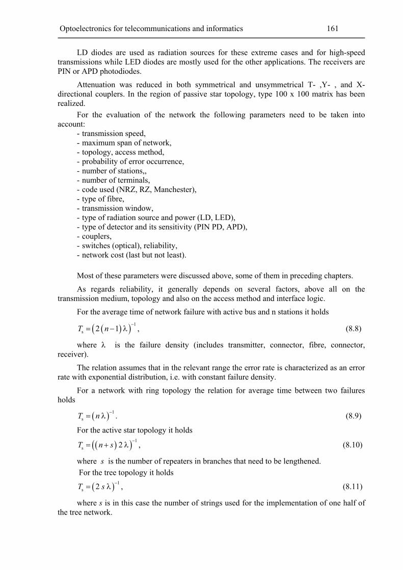
Optoelectronics for telecommunications and informatics 161
LD diodes are used as radiation sources for these extreme cases and for high-speed transmissions while LED diodes are mostly used for the other applications. The receivers are PIN or APD photodiodes.
Attenuation was reduced in both symmetrical and unsymmetrical T- ,Y- , and X-directional couplers. In the region of passive star topology, type 100 x 100 matrix has been realized.
For the evaluation of the network the following parameters need to be taken into account:
- transmission speed, - maximum span of network, - topology, access method, - probability of error occurrence, - number of stations,, - number of terminals, - code used (NRZ, RZ, Manchester), - type of fibre, - transmission window, - type of radiation source and power (LD, LED), - type of detector and its sensitivity (PIN PD, APD), - couplers, - switches (optical), reliability, - network cost (last but not least).
Most of these parameters were discussed above, some of them in preceding chapters.
As regards reliability, it generally depends on several factors, above all on the transmission medium, topology and also on the access method and interface logic.
For the average time of network failure with active bus and n stations it holds
1
s 2 1 ,T n
(8.8)
where λ is the failure density (includes transmitter, connector, fibre, connector, receiver).
The relation assumes that in the relevant range the error rate is characterized as an error rate with exponential distribution, i.e. with constant failure density.
For a network with ring topology the relation for average time between two failures holds
1
s .T n (8.9)
For the active star topology it holds
1
s 2 ,T n s
(8.10)
where s is the number of repeaters in branches that need to be lengthened.
For the tree topology it holds
1
s 2 ,T s (8.11)
where s is in this case the number of strings used for the implementation of one half of the tree network.

162 FEEC Brno University of Technology
For the active loop topology it holds for the average time between failures
.12 1s
nT (8.12)
In order to increase reliability, the network is often doubled. Some practical implementations of local optical networks
C&C Net Loop 6830
This local optical network was designed by the Japanese company NEC Corporation. The doubled optical fibre network consists of a central station (CS) and several terminal data stations (TDS), which are interconnected by this network. The basic schematic of this ring topology is given in Fig. 8.37. CS mostly has the function of network control while TDS forms the interface for the connection of various terminal devices.
Obr. 8.37: Concept of NET LOOP 6830 network
Basic characteristics of the network: - transmission speed 32 Mbit . s-1, - network range 2 km, - double-ring topology, - synchronous or asynchronous operation, - maximum number of TDS stations 64, - RZ code, - multimode gradient fibre (50/125 µm), - first transmission window, - radiation source NDL 4103 A (NEC), GaA1As DH LED, - radiation detector NDL 2102 (NEC) Si PIN FD, - error occurrence probability PE = 10-10.
Transmission is realized using the TOKEN method, data are transferred by means of packets (HDLC procedures), and transmission of video signals is also possible.
Schematic diagram of the module of optical interface is given in Fig. 8.38 [8-10].

Optoelectronics for telecommunications and informatics 163
Obr. 8.38: Optical interface module
Example of FDDI (Fibre Distributed Data Interface) network FDDI defines ring topology LON with these parameters:
- transmission speed 100 Mbit . s-1 - network range as much as 100 km, - double-ring topology, - maximum number of stations 500, - code 4B/5B, - gradient multimode fibre 62.5/125 μm or 85/125 µm, - wavelength regions of first or second transmission windows, - radiation source LED, LD, - radiation detector PIN PD.
FDDI enables building a high-capacity bus of computers or other LAN networks on the
premises of industrial plants, institutions, etc. The conversion of different protocols, speeds, data formats, etc. of these networks is performed by the so-called gateway. One variant of the FDDI network is shown in Fig. 8.39. As can be seen in the figure, various local networks are connected to this network (ETHERNET acc. to IEEE 802.3 recommendation, TOKEN RING acc. to IEEE 802.5 recommendation) as well as a private branch exchange (PBX). Building such networks enables easier integration of PBX exchanges and computers, and also simultaneous integration of LAN, LON and ISDN networks (integrated services digital network).

164 FEEC Brno University of Technology
Obr. 8.39: Variant of FDDI network
High transmission speed also enables creating links among computers, between computers and peripheral units (multiprocessor systems, systems CAD, CAE, and CAM) using the FDDI “Back-end” network.
When the double-ring topology is used, the second fibre is used not only for the reserve but also for transmission, and network throughput can thus be increased to 200 Mbit . s-1. In practical implementations the first fibre mostly interconnects all the subscribers (primary line) while the second fibre interconnects only selected subscribers (secondary line), as shown in Fig. 8.40. Type A station (connection to both fibres) contains one MAC (Media Access Controller) block and two PHY/PMD (Physical Media Dependent) blocks, which provide connection to both fibres. Type B stations lack this feature; they can only be connected to one ring (1 MAC block and 1 PHY/PMD block). Type B stations are less important stations.
Obr. 8.40: Configuration of network with double ring
The cable itself contains two optical fibres provided with a connector. In the case of station A one fibre forms the above-mentioned primary network, the other fibre forms the

Optoelectronics for telecommunications and informatics 165
secondary network. In the case of station B the same cable transmits incoming signals along one fibre and outgoing signals along the other fibre.
When there is a failure in one fibre (not necessarily a mechanical failure, also increased error rate, etc.), operation passes onto the other fibre within a few milliseconds. When there is a failure in the cable between stations, alternate operation is chosen depending on the topology shown in Fig. 8.41.
Obr. 8.41: Change in configuration in case of cable failure
FDDI uses the 4B5B code, which allows obtaining a lower modulation speed of 125 Mbit . s-1 and using cheaper components, manufactured by the LED technology, in the implementation of the transmitter and receiver.
The network itself is formed by stations connected in series in closed ring. Information is successively transmitted from one station to another. The station has the right to transmit as soon as it receives the “carrier”, which is a special packet that circulates along the ring after the last information packet. Its format is given in Fig. 8.42. Each station in the network supervises the carrier circulation time, from which the network load can be inferred. In the case of heavy load it is possible to transmit only the group of high-priority packets (designated synchronous). The other transmissions can only take place when the circulation time of the “carrier” is shorter than an agreed time value.
Obr. 8.42: Carrier and information packet formats: PA – PREAMBLE separator for synchronous receivers, SD – separator for indicating the packet beginning, FC – control bits for ensuring priority access to transmission medium, DA – address of station receiver, SA – address of station transmitter, INFO – information (data, 4500 bytes at the most), FCS – protection, EDF – separator for indicating the end of transmitting information, EDT – separator for indicating the end of transmission on the carrier, FS – control bits for indication of transmission errors.

166 FEEC Brno University of Technology
The time of “carrier” run tRT is directly proportional to the operational load on the ring. For ordinary operation it is guaranteed that the value of tRT never exceeds 2 . topr (topr is the reference quantity of carrier circulation). Stations with synchronous operation are guaranteed at least one transmission in every interval 2 . topr.
The total synchronous operational load is given by the sum of synchronous operational loads of all stations. If tRT < topr the operational load is small and at that moment asynchronous operation can start. Operation importance is given by the priorities. This solution of time supervision represents a simple and efficient means of controlling the operation on the ring, with the possibility of dynamic priority in dependence on operational load.
All failure functions are revealed when tRT > 2 . topr. In such cases it is necessary to launch procedures for failure localization as well as procedures for network reconfiguration.
The circuits AM 7984 and AM 7985 implement the functions of the PHY block, i.e. parallel-to-series data conversion for optical transmitter, series-to-parallel data conversion, 4B/5B coding, and compensation of the time shift of synchronization clock pulses.
The circuit AM 79083 implements access to transmission medium, inclusive of carrier restoration. It contains the detector and address generator, register of normal and error reports from transmission medium, generator and canceller of own carriers, detector and generator of CRC protection polynomial, and register of status word and failure states
FDDI is a powerful network that offers great possibilities and was expected to become number one in LON but it failed to achieve supremacy. Specific design elements for this network (optical cables, connectors) were to have ensured the production of and market for these elements but the development took an easier path – towards Ethernet [8-11].
LON FIBERCOM This local optical network is designed for industrial applications, offices, laboratories,
schools, the military, and others, enabling mutual interconnection of microcomputers, PC, terminals, printers, modems, and other devices provided with standard interface. It is a follow-up to the Ethernet standard, i.e. a compatible device.
Basic network characteristics:
- transmission speed 100 Mbit . s-1, - network range 2 km, - ring topology, - maximum number of stations 1024, - access method CSMA/CD, - compatible operating systems: MS-DOS, CP[M, Unix, - gateways: SNA/SDLC, Ethernet, X.25, HDLC. The network is shown in Fig. 8.43 [8-12].
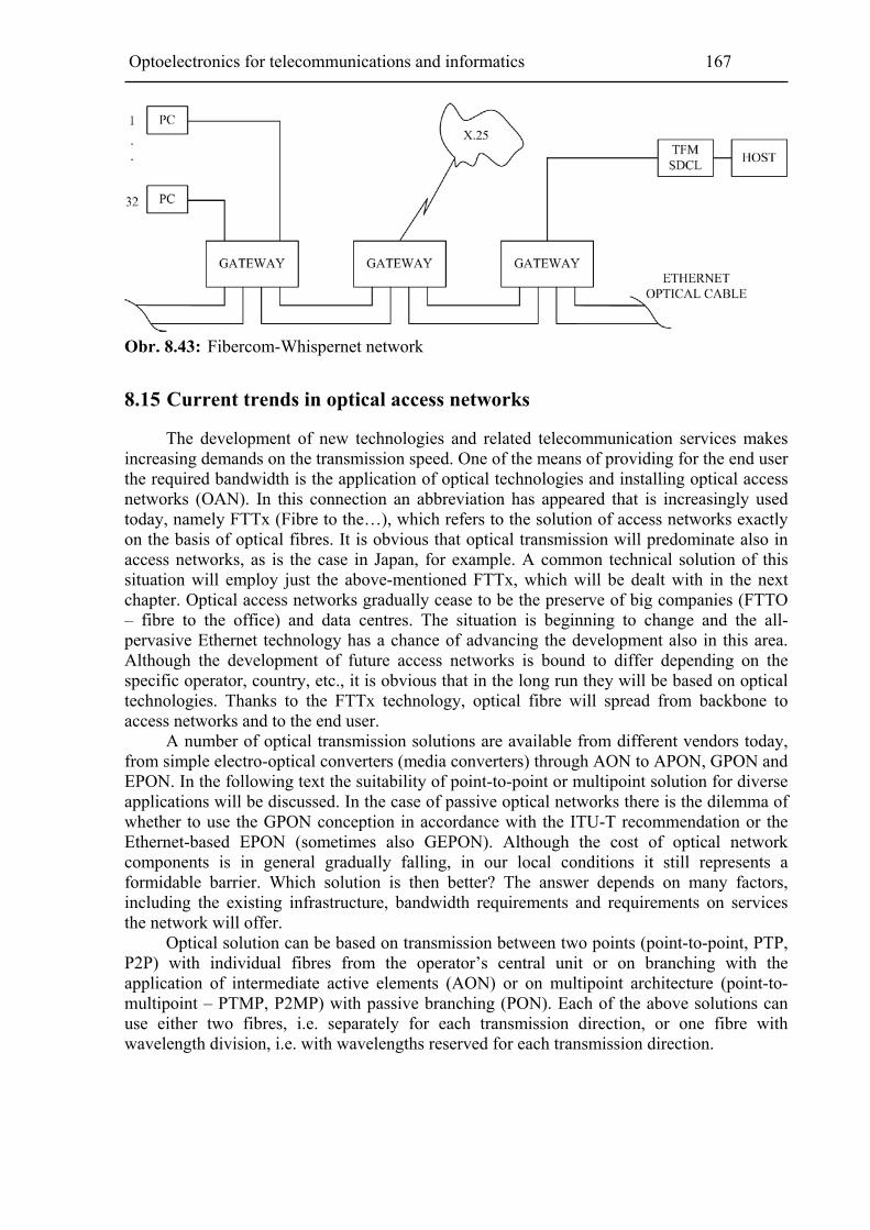
Optoelectronics for telecommunications and informatics 167
Obr. 8.43: Fibercom-Whispernet network
8.15 Current trends in optical access networks
The development of new technologies and related telecommunication services makes increasing demands on the transmission speed. One of the means of providing for the end user the required bandwidth is the application of optical technologies and installing optical access networks (OAN). In this connection an abbreviation has appeared that is increasingly used today, namely FTTx (Fibre to the…), which refers to the solution of access networks exactly on the basis of optical fibres. It is obvious that optical transmission will predominate also in access networks, as is the case in Japan, for example. A common technical solution of this situation will employ just the above-mentioned FTTx, which will be dealt with in the next chapter. Optical access networks gradually cease to be the preserve of big companies (FTTO – fibre to the office) and data centres. The situation is beginning to change and the all-pervasive Ethernet technology has a chance of advancing the development also in this area. Although the development of future access networks is bound to differ depending on the specific operator, country, etc., it is obvious that in the long run they will be based on optical technologies. Thanks to the FTTx technology, optical fibre will spread from backbone to access networks and to the end user. A number of optical transmission solutions are available from different vendors today, from simple electro-optical converters (media converters) through AON to APON, GPON and EPON. In the following text the suitability of point-to-point or multipoint solution for diverse applications will be discussed. In the case of passive optical networks there is the dilemma of whether to use the GPON conception in accordance with the ITU-T recommendation or the Ethernet-based EPON (sometimes also GEPON). Although the cost of optical network components is in general gradually falling, in our local conditions it still represents a formidable barrier. Which solution is then better? The answer depends on many factors, including the existing infrastructure, bandwidth requirements and requirements on services the network will offer. Optical solution can be based on transmission between two points (point-to-point, PTP, P2P) with individual fibres from the operator’s central unit or on branching with the application of intermediate active elements (AON) or on multipoint architecture (point-to-multipoint – PTMP, P2MP) with passive branching (PON). Each of the above solutions can use either two fibres, i.e. separately for each transmission direction, or one fibre with wavelength division, i.e. with wavelengths reserved for each transmission direction.

168 FEEC Brno University of Technology
PON (Passive Optical Network) Passive optical network (PON) is composed of OLT (Optical Line Termination) located in the CO (Central Office) and a set of interconnected ONT (Optical Network Terminal), which serve to terminate the fibre and convert optical signal to electric signal (usually located on the customer’s premises). Both devices (PLT and ONT) require voltage supply. PON got its name due to the fact that on the route between OLT and ONT it does not use active elements that need to be supplied but uses splitters and couplers to divide and distribute the fiber transmission capacity among end users – usually 32 end users over a distance of 10-20 km. And since this is a shared network, it is sometimes also referred to as P2MP (Pont To Multipoint). AON (Active Optical Network) Active optical network (AON) is very similar to passive optical network (PON) although there are three main differences. Along the route it does not use passive elements; it uses elements of the Ethernet network for outdoor application, which provide access to the fibre and aggregation. Instead of sharing the transmission bandwidth among several end users, this solution prefers a reserved channel for each user so that the channel is fully bidirectional, unlike in ADSL, where upload does not equal download. Because of its technology, this architecture is often referred to as P2P (Point To Point). The third difference in comparison with PON is the maximum route length. In PON the most remote end user must be 10 to 20 km from CO (in dependence on concrete conditions and the number of splitters used). On the other hand, the distance limit for AON is ca. 80 km, in dependence on the number of users that are to be served. In this case the number of users is given by the number of switches used and not by the infrastructure itself, as was the case of PON. The basic functional units forming the optical access network are:
- Optical line termination (OLT), which is provided by the function of network interface between the access network and the network providing telecommunication services, - Optical distribution network (ODN), which is a set of optical transmission devices between OLT and ONU, - Optical network units (ONU), which provide the functions of interface between the optical and the metallic parts of access networks, - Optical network terminals (ONT), which provide the functions of subscriber interface between subscriber terminals and access network (VoIP, video, data), see Fig. 8.44.
Obr. 8.44: Block diagram of access network
From the viewpoint of optical network units (ONU) in optical access networks and the manner of their execution, i.e. depending on where in the network the optical fibre is terminated, different types of optical access networks are distinguished; the following are usually given as the basic types:

Optoelectronics for telecommunications and informatics 169
- FTTC (Fibre To The Curb), optical fibres are brought to the subscriber’s optical switchbox and the terminal points of the network are connected to it via metallic cables,
- FTTB (Fibre To The Building), optical fibres are brought to the subscribers’ buildings and individual subscribers are connected via internal network,
- FTTO (Fibre To The Office), optical fibres are brought to a device (PC), - FTTH (Fibre To The Home), optical fibres are brought as far as subscriber sockets, - FTTCab (Fibre To The Cabinet), optical fibres are brought to rooms of subscribers
with great demands for transmission capacity. The main function of access networks consists in providing transport services in the
duplex mode. Signal transmission in both directions can be provided in several ways: - Simplex with SDM (Space Division Multiplex); transmission in either direction is provided along one optical fibre,
- Duplex with WDM (Wavelength Division Multiplex); along one optical fibre, with 1550 nm wavelength for downstream, and 1310 nm wavelength for upstream,
- Duplex with FDM (Frequency Division Multiplex); one optical fibre and one wavelength are used for signal transmission in both directions, transmission directions are frequency-divided.
The parameter that determines the nature of access network is the type of transmission track used in the distribution part of network:
- point-point P2P (Point-to-Point), e.g. direct connection of OLT and ONT, - multipoint P2M (Point-to-Multipoint), e.g. passive optical network.
Optical splitters
Optical splitters are network elements that enable optical transmission medium to be shared by a great number of subscribers. In the FTTH systems, which are operated in PON networks, they are usually bidirectional passive elements that have one input port and several (2 – 128) output ports. In downstream direction, the signal coming from the OLT to the input port of splitter is divided into the required number of partial signals, which are then distributed via output ports to individual ONU units. In the opposite (upstream) direction the splitter combines the signals coming from individual ONU units into a single signal, which is further distributed to OLT.
Splitters are passive network elements that only perform the splitting or merging of optical signals, without any further modification. Depending on the type and manufacturing technology, they can operate either in a certain transmission band or over its whole width. Using a splitter will insert attenuation in the optical route, whose value depends on the number of output ports and is given in dB, see Table 8.2 (for a division ratio of 1:32) [8-13], [8-14].
Tab. 8.2: Values of insertion attenuation for PLC splitter Telecordia GR-1209
1 x 4 1 x 8 1 x 16 1 x 32
Wavelength [nm] 1260 – 1650
Value of insertion attenuation [dB] 6,6 9,8 12,7 15,8
Maximum value of insertion attenuation [dB] 7,1 10,2 13,2 16,6
Splitters can be cascaded in dependence on network topology. But it is necessary to comply with the ITU-T recommendations, which regulate the attenuation values inserted in the optical route due to splitter application.
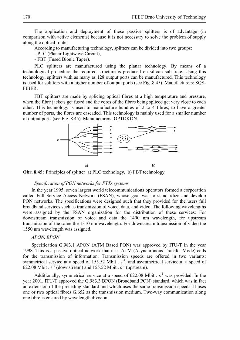
170 FEEC Brno University of Technology
The application and deployment of these passive splitters is of advantage (in comparison with active elements) because it is not necessary to solve the problem of supply along the optical route. According to manufacturing technology, splitters can be divided into two groups:
- PLC (Planar Lightwave Circuit), - FBT (Fused Bionic Taper).
PLC splitters are manufactured using the planar technology. By means of a technological procedure the required structure is produced on silicon substrate. Using this technology, splitters with as many as 128 output ports can be manufactured. This technology is used for splitters with a higher number of output ports (see Fig. 8.45). Manufacturers: SQS-FIBER.
FBT splitters are made by splicing optical fibres at a high temperature and pressure, when the fibre jackets get fused and the cores of the fibres being spliced get very close to each other. This technology is used to manufacture bundles of 2 to 4 fibres; to have a greater number of ports, the fibres are cascaded. This technology is mainly used for a smaller number of output ports (see Fig. 8.45). Manufacturers: OPTOKON.
Obr. 8.45: Principles of splitter a) PLC technology, b) FBT technology
Specification of PON networks for FTTx systems
In the year 1995, seven largest world telecommunications operators formed a corporation called Full Service Access Network (FSAN), whose goal was to standardize and develop PON networks. The specifications were designed such that they provided for the users full broadband services such as transmission of voice, data, and video. The following wavelengths were assigned by the FSAN organization for the distribution of these services: For downstream transmission of voice and data the 1490 nm wavelength, for upstream transmission of the same the 1310 nm wavelength. For downstream transmission of video the 1550 nm wavelength was assigned.
APON, BPON
Specification G.983.1 APON (ATM Based PON) was approved by ITU-T in the year 1998. This is a passive optical network that uses ATM (Asynchronous Transfer Mode) cells for the transmission of information. Transmission speeds are offered in two variants: symmetrical service at a speed of 155.52 Mbit . s-1, and asymmetrical service at a speed of 622.08 Mbit . s-1 (downstream) and 155.52 Mbit . s-1 (upstream).
Additionally, symmetrical service at a speed of 622.08 Mbit . s-1 was provided. In the year 2001, ITU-T approved the G.983.3 BPON (Broadband PON) standard, which was in fact an extension of the preceding standard and which uses the same transmission speeds. It uses one or two optical fibres G.652 as the transmission medium. Two-way communication along one fibre is ensured by wavelength division.

Optoelectronics for telecommunications and informatics 171
GPON
In the year 2003, ITU-T approved the specification G.984.1 GPON (Gigabit Capable PON), which starts from the G.983.X specification. It enlarges the G.983.1 specification as regards the speed while preserving the principles of broadband access system. For transmission it employs ATM cells and also the GEM (GPON Encapsulation Method) method. This method is used to transmit GPON frames, which are of variable lengths. ATM cells and GEM frames or their fragments are transmitted together in frames of fixed 125 μm length. This enables making use of packet-oriented services such as Ethernet or IP (Internet Protocol). Transmission speeds are offered in two variants: symmetrical service at speeds of 1244.16 Mbit . s-1 and 2488.32 Mbit . s-1, and asymmetrical service (downstream) at speeds of 1244.16 Mbit . s-1 and 2488.32 Mbit . s-1, and upstream at 155.52 Mbit . s-1, 622.08 Mbit . s-1, and 1244.16 Mbit . s-1.
EPON
By endorsing the IEEE 802.3ah specification, IEEE assured the introduction of Ethernet in access networks. This specification is usually referred to as EPON (Ethernet Based PON) or also EFMF (Ethernet In First Mile Fibre). The aim was to bring the Ethernet standard to the very user and thus to simplify the coupling of local networks. For the transmission in both directions Ethernet frames of fixed 2 ms length are used. EPON is designed for the multipoint network sharing one transmission medium but point-to-point communication can be emulated (P2PE Point To Point Emulation). The IEEE 802.3ah standard specifies two types of interface, which differ in the dynamics and optical powers. Type 1000Base-PX10 is designed for application over distances of up to 10 km, with maximum branching 1:16. Type 1000Base-PX20 is designed for distances of up to 20 km, with maximum branching 1:32. The transmission speed was set at 1244.26 Mbit . s-1, symmetrical.
Triple Play Services in FTTH Systems
The current trend among telecommunications operators and providers of broadband services is to offer the end user the broadest possible transmission band and the related services. Growing competition and desired cost-effectiveness makes operators implement ever new services. One of them is the “Triple Play” service. This is a new generation of services that offer transmission of voice, data, and video. The basic services are not billed singly since they are included in the flat rate for the connection to broadband network. Services that are beyond the frame of basic services are billed.
Methods of distributing video signal
Offering a wide choice of video and voice services is the main trend among telecommunications operators. No wonder, because they form a major part of their income. Much effort is therefore invested not only in deploying new services but also in seeking the most suitable transmission form that could introduce more services at the same time, without the need of extending the transmission bandwidth; this would increase the provider’s income. Video services offered within the frame of “Triple Play” are distributed among users in two ways, namely through the so-called overlay PON (Video Overlay Passive Optical Network) or through IPTV (TV over Internet Protocol).
For video transmission, overlay PON networks use the 1550 nm wavelength, which has been reserved for this service by ITU-T. The signal together with the data flow (data and voice) is transmitted to the user along one optical fibre, for which the 1490 nm wavelength is reserved using the wavelength division multiplex WDM. Both analogue and digital signals can be transmitted. At the user side the video signal is separated in the ONT unit (by means of
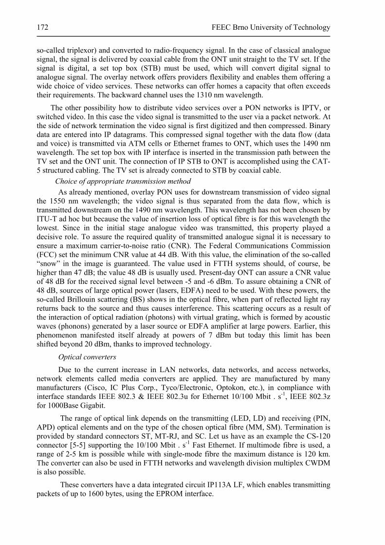
172 FEEC Brno University of Technology
so-called triplexor) and converted to radio-frequency signal. In the case of classical analogue signal, the signal is delivered by coaxial cable from the ONT unit straight to the TV set. If the signal is digital, a set top box (STB) must be used, which will convert digital signal to analogue signal. The overlay network offers providers flexibility and enables them offering a wide choice of video services. These networks can offer homes a capacity that often exceeds their requirements. The backward channel uses the 1310 nm wavelength.
The other possibility how to distribute video services over a PON networks is IPTV, or switched video. In this case the video signal is transmitted to the user via a packet network. At the side of network termination the video signal is first digitized and then compressed. Binary data are entered into IP datagrams. This compressed signal together with the data flow (data and voice) is transmitted via ATM cells or Ethernet frames to ONT, which uses the 1490 nm wavelength. The set top box with IP interface is inserted in the transmission path between the TV set and the ONT unit. The connection of IP STB to ONT is accomplished using the CAT-5 structured cabling. The TV set is already connected to STB by coaxial cable.
Choice of appropriate transmission method
As already mentioned, overlay PON uses for downstream transmission of video signal the 1550 nm wavelength; the video signal is thus separated from the data flow, which is transmitted downstream on the 1490 nm wavelength. This wavelength has not been chosen by ITU-T ad hoc but because the value of insertion loss of optical fibre is for this wavelength the lowest. Since in the initial stage analogue video was transmitted, this property played a decisive role. To assure the required quality of transmitted analogue signal it is necessary to ensure a maximum carrier-to-noise ratio (CNR). The Federal Communications Commission (FCC) set the minimum CNR value at 44 dB. With this value, the elimination of the so-called “snow” in the image is guaranteed. The value used in FTTH systems should, of course, be higher than 47 dB; the value 48 dB is usually used. Present-day ONT can assure a CNR value of 48 dB for the received signal level between -5 and -6 dBm. To assure obtaining a CNR of 48 dB, sources of large optical power (lasers, EDFA) need to be used. With these powers, the so-called Brillouin scattering (BS) shows in the optical fibre, when part of reflected light ray returns back to the source and thus causes interference. This scattering occurs as a result of the interaction of optical radiation (photons) with virtual grating, which is formed by acoustic waves (phonons) generated by a laser source or EDFA amplifier at large powers. Earlier, this phenomenon manifested itself already at powers of 7 dBm but today this limit has been shifted beyond 20 dBm, thanks to improved technology.
Optical converters
Due to the current increase in LAN networks, data networks, and access networks, network elements called media converters are applied. They are manufactured by many manufacturers (Cisco, IC Plus Corp., Tyco/Electronic, Optokon, etc.), in compliance with interface standards IEEE 802.3 & IEEE 802.3u for Ethernet 10/100 Mbit . s-1, IEEE 802.3z for 1000Base Gigabit.
The range of optical link depends on the transmitting (LED, LD) and receiving (PIN, APD) optical elements and on the type of the chosen optical fibre (MM, SM). Termination is provided by standard connectors ST, MT-RJ, and SC. Let us have as an example the CS-120 connector [5-5] supporting the 10/100 Mbit . s-1 Fast Ethernet. If multimode fibre is used, a range of 2-5 km is possible while with single-mode fibre the maximum distance is 120 km. The converter can also be used in FTTH networks and wavelength division multiplex CWDM is also possible.
These converters have a data integrated circuit IP113A LF, which enables transmitting packets of up to 1600 bytes, using the EPROM interface.
Optoelectronics for telecommunications and informatics 173
The CS-1200 series supports 1 Gbit . s-1, Gigabit Ethernet. It fulfils the recommendations IEEE 802.3zD2 GBIC (Gigabit Interface Converters) and MSA (Multi Source Agreement).
In the VCSEL (Vertical Cavity Surface Emitting Laser) transmitting part the 850 nm wavelength can be used. For single-mode transmission on the 1310 nm wavelength the FP (Fabry-Perot) laser is used while for the 1550 nm wavelength the DFB (Distributed Feedback) laser is used, which allows the deployment of the CWDM multiplex, with 20 nm channel spacing in the 1310-1610 nm waveband. For the MM fibre the range is up to 550 , for the SM fibre it is as much as 120 km. Optical output can be solved using duplex connectors SC and LC or Bi-Di (bidirectional) single connectors LC and SC.
The receiving part consists of a high-sensitivity GaAs PIN or InGaAs Pin photodiode, with high sensitivity, possibly also with application of optical amplifier. The receiver enables using the waveband of 1100 to 1600 nm.
The converters also satisfy the respective standards for the supply and for the diagnostics of function and failure conditions.
At the exchange side the converters are mounted in switchboards (box – chassis) with connection via UTP cables to switches. A network made up in this way can be monitored from the viewpoint of failure conditions (supervision system).
Work is currently continuing on changing over to higher speeds, 10 Gbit . s-1, with commensurably increased range. Standards XENPAK, X2, XFP, and SFP+.
8.16 Optoelectronic multipley systems
The present information explosion makes increasing demands on the number of transmitted channels and this is the reason why signals are multiplexed on links. The following methods of multiple transmission are in existence:
- frequency division multiplex: individual signals are transferred to higher frequency bands and so-called modulation groups are formed which are modulated to an optical signal generated by laser or light-emitting diode. The whole multiplex system remains in the region of electronic circuits; the potentials of this multiple transmission are limited by the parameters of sources of optical radiation,
- time division multiplex: each signal is assigned a time interval in which at the transmitting side the transmitter and at he receiving side the receiver of the given signal are connected,
- electronic multiplex: not a binary signal but a multiple signal is transmitted along one fibre, which increases the transmission speed n-times,
- space division multiplex: it uses several fibres to transmit different signals, - wavelength division multiplex: it makes use of the possibility of radiation from
various sources of light of different wavelengths, which are modulated by individual information sources (the respective “windows” in regions of minimum fibre attenuation are used for the transmission),
- hybrid multiplex: it represents the combination of wavelength division multiplex with electronic multiplex (enabling maximum exploitation of the transmission potentials of fibre).
In view of the fact that as regards the exploitation of transmission capacity of optical fibre the most advantageous is the wavelength division multiplex (hybrid multiplex)

174 FEEC Brno University of Technology
we will deal with it in detail below. The other principles, given earlier, are generally known and some of them trivial (see space division multiplex).
The classical optoelectronic link, described on several earlier occasions, enables one-way operation between the transmitter and receiver (simplex link); when more fibres are used, the space division multiplex can be formed (Fig. 8.46a). If two-way operation along one fibre is needed, connection according to Fig. 8.46b can be used, i.e. duplex connection. In such a connection, transmitter V1 and receiver P1 operate together on wavelength λ1, transmitter V2 and receiver P2 on wavelength λ2. Wavelengths from the fibre are combined and divided in a duplexer. In the case of using several radiation emitters on different wavelengths, coupled by means of multiplexer to one optical fibre, we speak about wavelength division multiplexer. At the receiver side, the demultiplexer is connected, whose task is to divide the respective wavelengths for individual receivers (Fig. 8.46c). To implement an n-channel link it is necessary to have n modulators, n optical sources and n detectors, one WDM (Wavelength Division Multiplexing) multiplexer and one demultiplexer (the pair is referred to as WDM muldex). Simple non-selective optical termination can be used in the function of multiplex. Optical demultiplexers, which must be implemented as optical filters, are more complex.
Obr. 8.46: Principle of multiplex a) space division multiplex, b) duplex, c) wavelength division multiplex
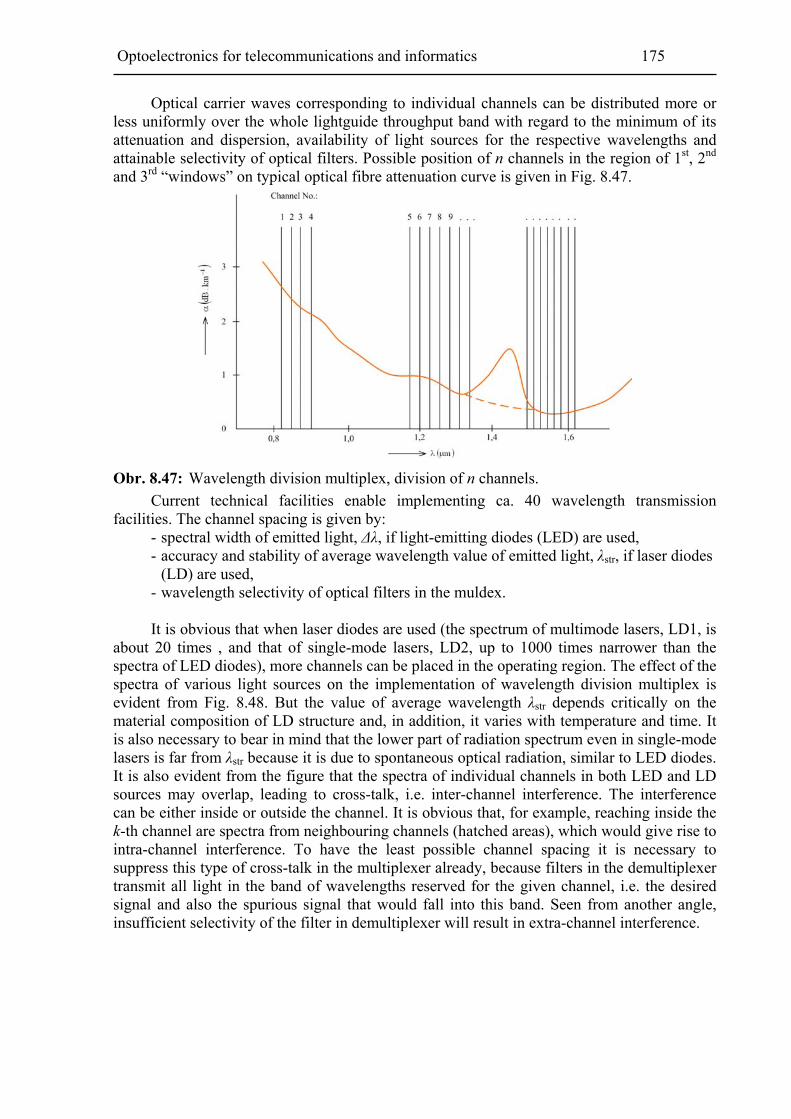
Optoelectronics for telecommunications and informatics 175
Optical carrier waves corresponding to individual channels can be distributed more or less uniformly over the whole lightguide throughput band with regard to the minimum of its attenuation and dispersion, availability of light sources for the respective wavelengths and attainable selectivity of optical filters. Possible position of n channels in the region of 1st, 2nd and 3rd “windows” on typical optical fibre attenuation curve is given in Fig. 8.47.
Obr. 8.47: Wavelength division multiplex, division of n channels.
Current technical facilities enable implementing ca. 40 wavelength transmission facilities. The channel spacing is given by:
- spectral width of emitted light, Δλ, if light-emitting diodes (LED) are used, - accuracy and stability of average wavelength value of emitted light, λstr, if laser diodes
(LD) are used, - wavelength selectivity of optical filters in the muldex. It is obvious that when laser diodes are used (the spectrum of multimode lasers, LD1, is
about 20 times , and that of single-mode lasers, LD2, up to 1000 times narrower than the spectra of LED diodes), more channels can be placed in the operating region. The effect of the spectra of various light sources on the implementation of wavelength division multiplex is evident from Fig. 8.48. But the value of average wavelength λstr depends critically on the material composition of LD structure and, in addition, it varies with temperature and time. It is also necessary to bear in mind that the lower part of radiation spectrum even in single-mode lasers is far from λstr because it is due to spontaneous optical radiation, similar to LED diodes. It is also evident from the figure that the spectra of individual channels in both LED and LD sources may overlap, leading to cross-talk, i.e. inter-channel interference. The interference can be either inside or outside the channel. It is obvious that, for example, reaching inside the k-th channel are spectra from neighbouring channels (hatched areas), which would give rise to intra-channel interference. To have the least possible channel spacing it is necessary to suppress this type of cross-talk in the multiplexer already, because filters in the demultiplexer transmit all light in the band of wavelengths reserved for the given channel, i.e. the desired signal and also the spurious signal that would fall into this band. Seen from another angle, insufficient selectivity of the filter in demultiplexer will result in extra-channel interference.

176 FEEC Brno University of Technology
Obr. 8.48: Spectra of LED, LD1 and LD2
On the basis of what has been said we can define channel spacing as the difference of two close wavelengths of optical radiation
.j1j (8.13)
The value Δλ depends on the radiation sources used and on the design of optical multiplexers and demultiplexers.
The spacing and wavelength selectivity of WDM multiplexer and demultiplexer are given by the pass-band width and the steepness of the sides of optical filter attenuation characteristics.
An important parameter of muldexes is their insertion loss. Insertion loss defines the losses that arise due to the passage of optical radiation through multiplexer or demultiplexer; they can be expressed by the relation
j vstj
j výst
10 log dB .P
aP
(8.14)
It is obvious that the value of insertion loss will be different for each wavelength. Optical multiplexer or demultiplexer is defined (evaluated) by the maximum value of insertion attenuation for the given type of system.
Another parameter for the evaluation of WDM multiplexer is cross-talk attenuation. It is expressed by the ratio of power Pλj vst to power Pλj, λi výst, where Pλj vst is the power of radiation entering the system on the wavelength λj while Pλj, λi výst is the power of radiation on the wavelength λj on the output for the wavelength λi.
.dBlog10výstij
vstjji
P
Pa (8.15)
The main task of the WDM multiplexer is thus to multiplex light beams from individual sources into a single lightguide. With small channel spacing the multiplexer must also contain wavelength-selective members (optical filters) for the purpose of suppressing intra-channel interference. The division of light beam into individual rays by wavelength is performed in demultiplexer. Demultiplexer must always contain wavelength-selective members; in some cases just the selectivity of photodetectors is made use of.
In duplex links, when the transmitter and receiver are connected to the same end of optical fibre, at least a coupler must be inserted between this pair and the fibre otherwise cross-talk would appear between the transmitter and receiver.

Optoelectronics for telecommunications and informatics 177
Wavelength-selective members used in muldex design are in most cases reciprocal, i.e. they can be used for both multiplexing and demultiplexing by simply interchanging the inputs and outputs. Depending on the method they use for their function, they can be divided into two groups:
- interference members, - dispersion members. Interference selective members make use of interference filters, which make light waves
either reflect from the filter or pass through the filter, depending on the wavelength of light. The filter itself is formed by 10 to 40 thin layers of dielectric material with alternately changing refractive index. A high reflectance for certain wavelengths is obtained by a suitable structure of the filter. The design of a demultiplexer with interference filters is shown in Fig. 8.49. The lenses are formed by glass cylinders, in which refractive index decreases from the axis to the rim so that the passing light beam gets focused. Insertion attenuation of muldexes with such filters increases roughly in proportion to the number of channels
Obr. 8.49: Interference demultiplexer
j dB ,a n (8.16)
a can therefore be used for multiplexers with a lower number of channels. Attenuation increases by n-fold reflection or by the passage of light through filters. The radiation sources may be both LED and LD diodes.
Dispersion filters make use of the separation of light, for example, by a prism or various optical gratings.
When light passes through a prism (Fig. 8.50), then due to the double refraction on border surfaces there is a refraction angle υ
min 2 arcsin sin ,2
n
(8.17)
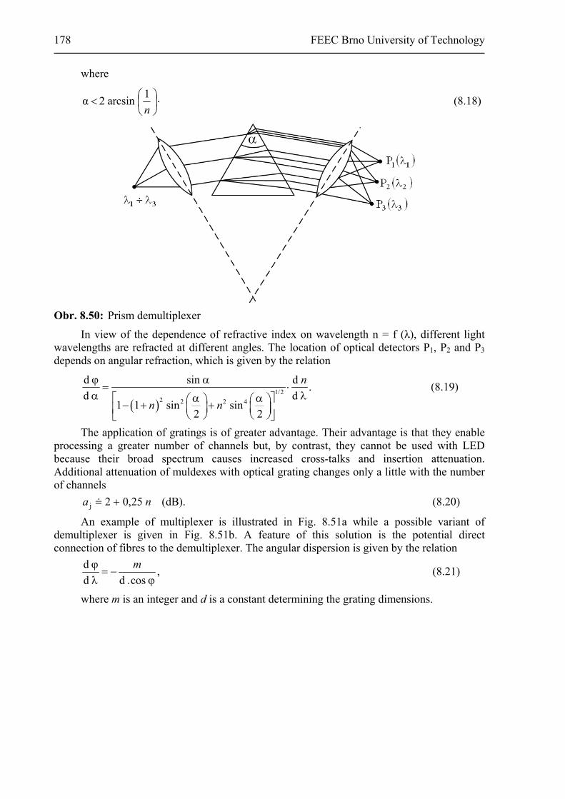
178 FEEC Brno University of Technology
where
n
1arcsin2α (8.18)
Obr. 8.50: Prism demultiplexer
In view of the dependence of refractive index on wavelength n = f (λ), different light wavelengths are refracted at different angles. The location of optical detectors P1, P2 and P3 depends on angular refraction, which is given by the relation
1/2
2 2 2 4
d sin d.
d d1 1 sin sin
2 2
n
n n
(8.19)
The application of gratings is of greater advantage. Their advantage is that they enable processing a greater number of channels but, by contrast, they cannot be used with LED because their broad spectrum causes increased cross-talks and insertion attenuation. Additional attenuation of muldexes with optical grating changes only a little with the number of channels
).dB(25,02j na (8.20)
An example of multiplexer is illustrated in Fig. 8.51a while a possible variant of demultiplexer is given in Fig. 8.51b. A feature of this solution is the potential direct connection of fibres to the demultiplexer. The angular dispersion is given by the relation
d,
d d .cos
m
(8.21)
where m is an integer and d is a constant determining the grating dimensions.
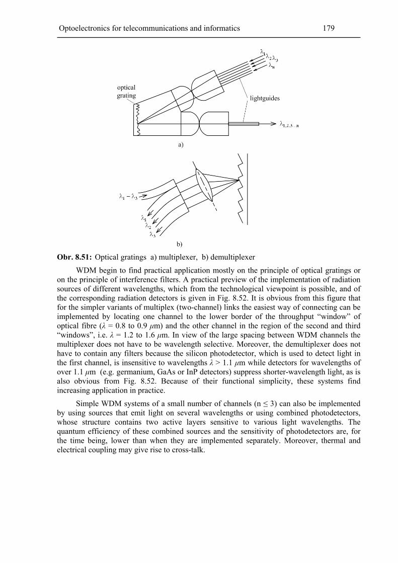
Optoelectronics for telecommunications and informatics 179
Obr. 8.51: Optical gratings a) multiplexer, b) demultiplexer
WDM begin to find practical application mostly on the principle of optical gratings or on the principle of interference filters. A practical preview of the implementation of radiation sources of different wavelengths, which from the technological viewpoint is possible, and of the corresponding radiation detectors is given in Fig. 8.52. It is obvious from this figure that for the simpler variants of multiplex (two-channel) links the easiest way of connecting can be implemented by locating one channel to the lower border of the throughput “window” of optical fibre (λ = 0.8 to 0.9 μm) and the other channel in the region of the second and third “windows”, i.e. λ = 1.2 to 1.6 μm. In view of the large spacing between WDM channels the multiplexer does not have to be wavelength selective. Moreover, the demultiplexer does not have to contain any filters because the silicon photodetector, which is used to detect light in the first channel, is insensitive to wavelengths λ > 1.1 μm while detectors for wavelengths of over 1.1 μm (e.g. germanium, GaAs or InP detectors) suppress shorter-wavelength light, as is also obvious from Fig. 8.52. Because of their functional simplicity, these systems find increasing application in practice.
Simple WDM systems of a small number of channels (n ≤ 3) can also be implemented by using sources that emit light on several wavelengths or using combined photodetectors, whose structure contains two active layers sensitive to various light wavelengths. The quantum efficiency of these combined sources and the sensitivity of photodetectors are, for the time being, lower than when they are implemented separately. Moreover, thermal and electrical coupling may give rise to cross-talk.
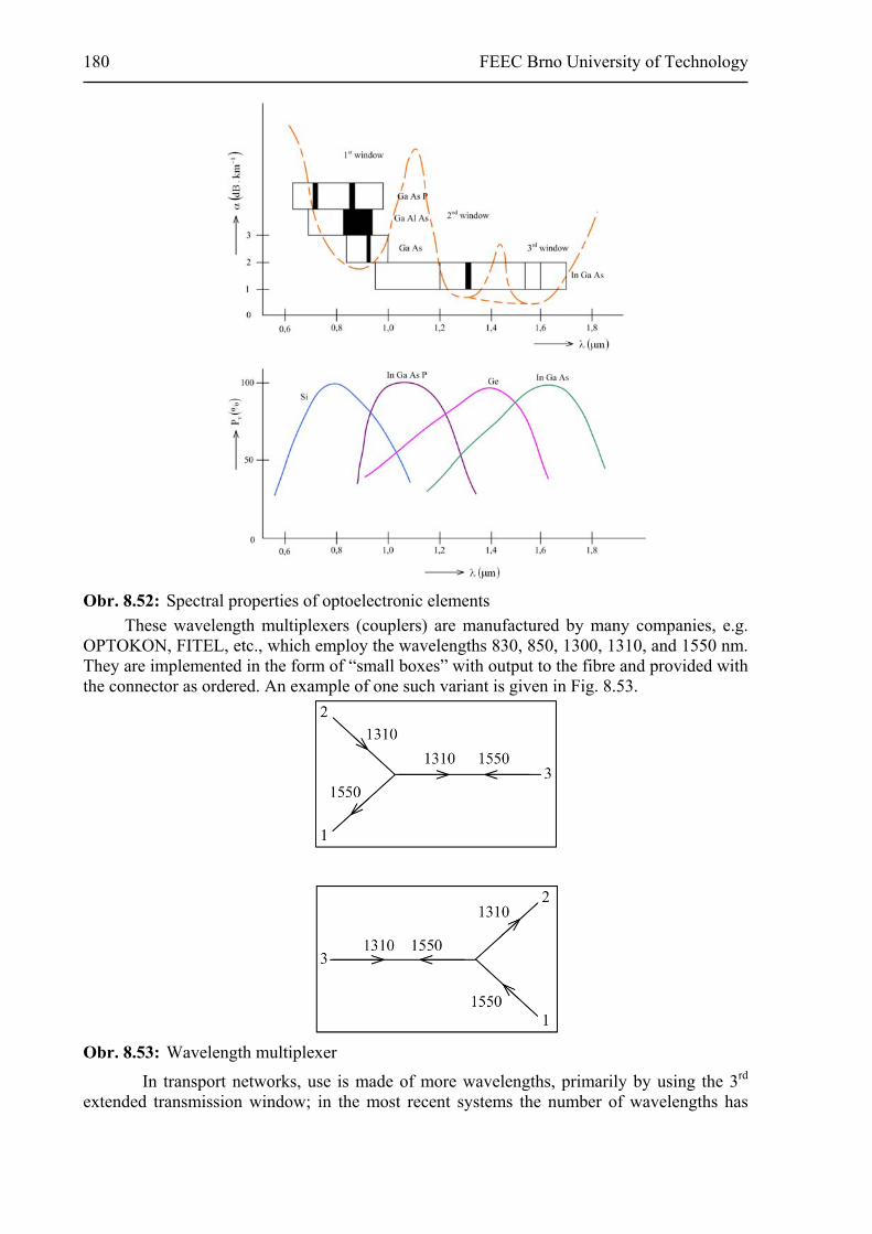
180 FEEC Brno University of Technology
Obr. 8.52: Spectral properties of optoelectronic elements
These wavelength multiplexers (couplers) are manufactured by many companies, e.g. OPTOKON, FITEL, etc., which employ the wavelengths 830, 850, 1300, 1310, and 1550 nm. They are implemented in the form of “small boxes” with output to the fibre and provided with the connector as ordered. An example of one such variant is given in Fig. 8.53.
Obr. 8.53: Wavelength multiplexer
In transport networks, use is made of more wavelengths, primarily by using the 3rd extended transmission window; in the most recent systems the number of wavelengths has

Optoelectronics for telecommunications and informatics 181
been increased into the removed “hump” on the attenuation curve (type All Wave fibres) as indicated by dashed line in Fig. 8.52.
Let us in the following have a look at these wavelength systems.
The initial wavelength multiplex uses for the transmission only two or three wavelengths, mostly in two-way operation on one optical fibre. The passive wavelength multiplexer WDM is a simple and cheap device.
WWDM technology
The wide wavelength division multiplexing (WWDM) mostly uses four wavelengths in the 850 nm region (multimode optical fibres) or in the 1300 and 1310 nm regions (multimode or single-mode optical fibres). Most frequently, the WWDM technology is employed for the transmission of Gigabit and 10 Gigabit Ethernet. Individual wavelengths of the WWDM multiplex have typically a spacing of 25 nm.
DWDM technology
The dense wavelength division multiplexing (DWDM) uses minimum spacing between individual channels so that it can implement tens of wavelengths in one fibre. Single-mode lasers and narrow-band interference filters are used in these cases. In addition, it is necessary to assure sufficient frequency stability and extremely narrow spectral lines. Laser stability is ensured either from outside (via injection synchronization, phase lock) or using distributed feedback or the Bragg mirrors. Since the selectivity of optical filters is of the order of 10 THz at best, the division of channels must be performed on intermediate frequency by means of electric filters, i.e. the receiver must contain a scrambler and a local oscillator in the form of frequency-stabilized highly coherent optical source.
In practical designs it is necessary to bear in mind that the range of individual channels will be different (the differences are quite large) and the worst transmission properties of a particular channel in the multiplex must be considered (or the worst channels not used).
The deployment of DWDM systems in commercial operation was conditional on the development and economically mastered production of key components such as erbium-doped fibre amplifiers (EDFA), multiplex and demultiplex units, and narrow-band laser transmitters. Thanks to the progress in the field of development and production but also thanks to the considerable demand for transmission capacity, the DWDM systems at the beginning of the 20th century began to be deployed in backbone transmission routes. The first functional DWDM devices came to the Czech Republic in the spring of 1999.
ITU-T recommendation G.694.1 “Spectral grids for WDM applications: DWDM frequency grid” specifies individual transmission channels in the wavelength region from 1490 nm (200.95 THz) to 1620 nm (186.00 THz) (so-called S, C and L bands). ITU-T recommendation G.694.1 specifies the spacing of individual channels in the range of 100 GHz, beginning on 186.00 THz (spacing ca. 0.8 nm) or twice as many channels with 50 GHz spacing (ca. 0.4 nm). In DWDM transmissions the required signal-to-noise ratio increases with increasing transmission speed in the channel. For example, for STM-16 (2.5 Gbit . s-1) 18 – 20 dB SNR is sufficient for good-quality transmission; for STM-64 (10 Gbit . s-1) 22 dB are required while for STM-256 (40 Gbit . s-1) ca. 25 dB are required. For good-quality transmission it is necessary for the actual wavelength of the channel (so-called maximum power wavelength) not to deviate from the prescribed wavelength (i.e. the nominal wavelength) by more than ± 0.2 of the spacing of carriers. For a 100 GHz spacing of the carriers it follows that the actual wavelength must be within the ± 20 GHz tolerance (this

182 FEEC Brno University of Technology
corresponds to ± 0.16 nm). The bandwidth of an optical signal transmitted in one channel depends on the bandwidth of the original modulating signal and it can be further impaired (extended) by using an inappropriate modulation technique.
CWDM technology
Coarse wavelength division multiplexing (CWDM) came into being as a cheaper variant of DWDM. The CWDM technology is a form of wavelength multiplexing that uses a larger spacing between individual transmission channels than is the case in the classical DWDM technology. In the recommendation ITU-T G.671 it was specified that the spacing of individual channels should be less than 50 nm; for the 1550 nm wavelength it should be 8 nm. It was only the advent of fix specification of individual wavelengths that provided a basis for the extensive development and mass deployment of this technology. In the year 2002, the Standards Commission of ITU issued the recommendation ITU-T G.694.2 “Spectral grids for WDM applications: CWDM wavelength grid.” Standard G.694.2 defines the size of spacing of individual wavelength channels for use in CWDM technology such that laser diodes could be used as radiation sources without cooling being required. Also, the individual wavelengths were chosen such that they were compatible with the conventional wavelengths 1310 nm and 1550 nm.
All the wavelengths of the CWDM technology (18 channels are available) can only be used with type “Metro” fiber, in other words with full spectrum according to the G.652.C standard. “Metro” is a type of fibre that is manufactured without increased attenuation in the region of the 1360 to 1450 nm wavelengths. In current cases of the existing optical routes, however, only the standard single-mode fibre 9/125 μm is mostly available, which corresponds to the ITU-T G.652 standard; 12 channels are available, with wavelengths of 1290, 1310, 1330, 1350, 1470, 1490, 1510, 1530, 1550, 1570, 1590, and 1610 nm.
CWDM finds application in metropolitan optical networks and in the optical-fibre solution of the “last mile” problematic. In access networks, xDSL providers can use CWDM to connect the digital loop carrier (DLC) to the central exchange. CWDM is most often used in point-to-point communication or in ring topologies of up to four nodes. CWDM can transmit Gigabit Ethernet over distances of up to 80 km; at STM-16 speeds (2.5 Gbit . s-1) the range is about 50 km.
Optical amplifiers
Optical amplifiers are used with advantage in wavelength division multiplexing systems. Unlike repeaters, they enable restoring luminous flux in the fibre without the necessity of converting it to electric form. These amplifiers are universal elements that amplify both analogous and digital signals of arbitrary transmission speed.
Optical fibre amplifiers EDFA (Erbium Doped Fibre Amplification)
A simplified block diagram of the EDFA amplifier is given in Fig. 8.54. The amplifier is formed by the so-called laser pump and a special optical fibre, which is doped with rare-earth elements (erbium, et al.). Due to the laser pump emission (of 980 nm or 1480 nm wavelength) coupled to a special fibre of several metres in length, atoms of doped element are excited to a higher energy level. The energy obtained from the laser pump radiation is thus temporarily stored in the atoms. This energy is released due to the presence of the signal being transmitted, whose energy calls forth stimulated emission of radiation, which is of the same wavelength and phase as the signal transmitted. This amplifies the transmitted optical signal. Optical fibre amplifiers enable increasing the signal level by as much as 50 dB (one channel, C – band). Via internal arrangement of the amplifier a wide range of the amplified band can be obtained and thus the signal can be amplified in the C and L bands simultaneously.

Optoelectronics for telecommunications and informatics 183
Various possibilities of deployment in an optical transmission system result from the principle of EDFA function. Basically, the amplifiers can be applied in four manners ([8-16]):
- Booster – which is located right after the optical transmitter; it serves to amplify its signal to a maximum level that can be coupled to the fibre. It must be capable of accommodating a relatively large input signal from optical transmitter.
- In-line amplifier – which is located on the optical fibre route; it amplifies a small input signal to a maximum output signal.
- Pre-amplifier - serves to amplify very low signal levels to a level that is sufficient for a correct functioning of optical amplifier at the end of transmission route. The requirement put on the pre-amplifier is to have a minimum internal noise.
- Compensation of losses in optical networks (CATV) – in optical community antenna television the reduction of signal level is primarily due to the requirement to divide the optical signal into several fibres. Before being divided the signal is amplified by means of EDFA such that the same signal level is obtained in output fibres as in the original fibre.
These amplifiers are manufactured as single-channel EDFA amplifiers, WDM amplifiers, and CATV amplifiers.
Obr. 8.54: Principle of optical EDFA amplifier
Optical Raman amplifiers
he Raman type of amplifiers is used to amplify an optical signal. It is practically just a laser source of radiation connected to the optical route. To amplify the optical signal the Raman scattering on particles of the waveguide material is used. With this scattering there is, among other things, a shift of energy from the lower wavelengths (wavelength of Raman pump radiation) to higher wavelengths (wavelengths of the signal being transmitted) and consequently an amplification of the signal. A simplified connection diagram is shown in Fig. 8.55.
Obr. 8.55: Optical Raman amplifier
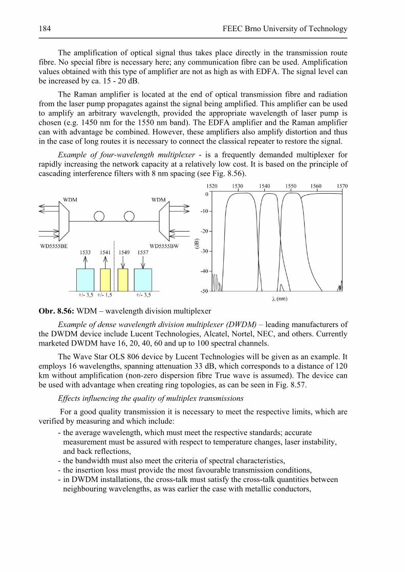
184 FEEC Brno University of Technology
The amplification of optical signal thus takes place directly in the transmission route fibre. No special fibre is necessary here; any communication fibre can be used. Amplification values obtained with this type of amplifier are not as high as with EDFA. The signal level can be increased by ca. 15 - 20 dB.
The Raman amplifier is located at the end of optical transmission fibre and radiation from the laser pump propagates against the signal being amplified. This amplifier can be used to amplify an arbitrary wavelength, provided the appropriate wavelength of laser pump is chosen (e.g. 1450 nm for the 1550 nm band). The EDFA amplifier and the Raman amplifier can with advantage be combined. However, these amplifiers also amplify distortion and thus in the case of long routes it is necessary to connect the classical repeater to restore the signal.
Example of four-wavelength multiplexer - is a frequently demanded multiplexer for rapidly increasing the network capacity at a relatively low cost. It is based on the principle of cascading interference filters with 8 nm spacing (see Fig. 8.56).
Obr. 8.56: WDM – wavelength division multiplexer
Example of dense wavelength division multiplexer (DWDM) – leading manufacturers of the DWDM device include Lucent Technologies, Alcatel, Nortel, NEC, and others. Currently marketed DWDM have 16, 20, 40, 60 and up to 100 spectral channels.
The Wave Star OLS 806 device by Lucent Technologies will be given as an example. It employs 16 wavelengths, spanning attenuation 33 dB, which corresponds to a distance of 120 km without amplification (non-zero dispersion fibre True wave is assumed). The device can be used with advantage when creating ring topologies, as can be seen in Fig. 8.57.
Effects influencing the quality of multiplex transmissions
For a good quality transmission it is necessary to meet the respective limits, which are verified by measuring and which include:
- the average wavelength, which must meet the respective standards; accurate measurement must be assured with respect to temperature changes, laser instability, and back reflections,
- the bandwidth must also meet the criteria of spectral characteristics, - the insertion loss must provide the most favourable transmission conditions, - in DWDM installations, the cross-talk must satisfy the cross-talk quantities between
neighbouring wavelengths, as was earlier the case with metallic conductors,

Optoelectronics for telecommunications and informatics 185
Obr. 8.57: OLS 806 in “ring application”
- the back reflection may be different in individual channels and the values need to be
kept within tolerances, mainly with a view to system stability, - the peak power of individual channels must satisfy the respective tolerances, - the type of fibre used is a separate and very important consideration.
An example of the spectral characteristics of four-wavelength multiplexer is shown in Fig. 8.58. In the case of new installation, when the deployment of DWDM system is assumed, the technical parameters can be selected to meet the operator’s requirement. This principle is currently implemented in the construction of transport networks of many operators, using the so-called “Telehouses”.
A substantially more difficult situation exists as regards the future exploitation of already installed fibres for the needs of DWDM.
In the first place, earlier fibres (ITU G.652) are not optimal for DWDM. Relatively large chromatic dispersion in the 1550 nm band limits the link range and compensation is necessary for longer routes.
Obr. 8.58: Spectrum of wavelength division multiplexer
All the effects given above influence transmission and they must be taken into consideration in the design of networks.

186 FEEC Brno University of Technology
Application potentials of wavelength division multiplexers in academic computer network of universities One of the first applications is the deployment of two-wavelength multiplexer in the experimental network of the Department of Telecommunications (DT). The system demonstrates its functionality and enables the measurement of elements. The system was used to demonstrate its application in the supervision for optical cables. Its connection is shown in Fig. 8.59.
Obr. 8.59: Implementation and connection of WDM in DT network
Experimental DWDM transmission in CESNET project
Given as an example will be the results of a DWDM transmission that was realized by CESNET workers [8-17]. The experiment was to prove, and it did prove, the possibility of two-way transmission by (2x4) 10 Gbit . s-1 Ethernet (GE) channels over a distance of 210 km without the necessity of connecting the EDFA link amplifier. This is the distance between Prague and Brno and the fibre used was standard single-mode fibre (G.652).
At the receiving and the transmitting sides 4 DWDM channels were combined (divided) by means of multiplexers (demultiplexers) with a phased series of waveguides. Following the transmitter, the signals were amplified in EDFA with 22 dB output power, and transmitted via polarization-independent insulators into a 210 km long standard single-mode fibre (G.652); the wavelength complied with the ITU-T standard, channels 34-37; channels 31, 32, 33, and 38 for reverse direction. Optical power of transmitters ca. 1 mW.
At the receiving side 4 DWDM channels were separated by polarization-independent optical circulator and amplified by low-noise EDFA pre-amplifier (Pvyst = 10 dBm). Chromatic dispersion of the fibre was compensated using the temperature-tuned DWDM Bragg grating (FBG); individual channels were demultiplexed via AWG (Array Waveguide Grating) and delivered to XENPAX receivers.
Optoelectronics for telecommunications and informatics 187
The results were evaluated by measuring the channel spacing and error rate. On the basis of analysis the hypothesis was formulated of potential 16 x 10 Gbit . s-1 transmission over a distance of up to 250 km (using EDFA with higher output power).
Further prospects of DWDM multiplexers
Increasing the speed will continue to be the main trend in further development. The maximum number of channels is being increased to 128 – 160. In experimental work as many as 1024 channels have been achieved. Other parallel bands, C and L, begin to be used. The universality of transmission medium increases, enabling e.g. the Gbit, 10 Gbit, Ethernet, and STM 64 transmissions. If systems with a capacity of 1.6 Tbit . s-1 are deployed today in backbone networks, this value can be expected to increase to 20 Tbit . s-1. As regards the distance, the use of Raman scattering and soliton transponders will increase the DWDM range to thousands of kilometres.
Network flexibility will be markedly increased by the application of Cross-Connects; they enable assuring the reconfiguration and stand-by of spectral channels in several milliseconds. These elements are currently implemented with a switching capacity of 1024 x 1024, the switching being performed on a chip by means of micro-electromechanical mirrors; the switching is 16 times faster than in current electronic switches.
Summing up we can say that these new technologies markedly enhance the offer of new services and transmission potentials in optical communications.
8.17 TV optical fibre links
The principle of cable television (CATV – Community Antenna Television) consists in that the TV centre receives television programmes from TV transmitter, satellite or directly from local studio and converts them to ordinary television bands and channels. The latter are then distributed through a single broadband branched cable with amplifiers. Every house or home can subscribe to the whole television programme on offer. Abroad, this service is used extensively. Not only does it enable increasing the number of channels, inclusive of satellite reception, but it also assures high quality reception of the signal, in particular at sites of weak reception (valleys, cities, etc.).
It is obvious that this service primarily attracts the interest of subscribers, in particular today, when operators offer Internet and telephone services.
Interest in the construction of these links also poses the question whether it would be of greater advantage to use optical fibre instead of the currently used coaxial cable. Fundamentally, the same problem is concerned here as outlined in the solution of FTTH networks.
Optical fibres are currently used by CATV operators for long-haul transmissions between the centre and a city (urban satellite); subscribers continue being connected via cheaper coaxial cables.
Already in present-day conditions we can see that three areas, namely telecommunications, radio-communications and computer technology begin to fuse, being increasingly dependent on one another.
However, the situation today is characterized by lack of coordination from the technical viewpoint and also as regards standardization, software, etc. The need will thus arise for systems with different internal architectures to cooperate. At the interfaces of these networks adapters will have to be installed that will interconnect and adapt the individual systems.
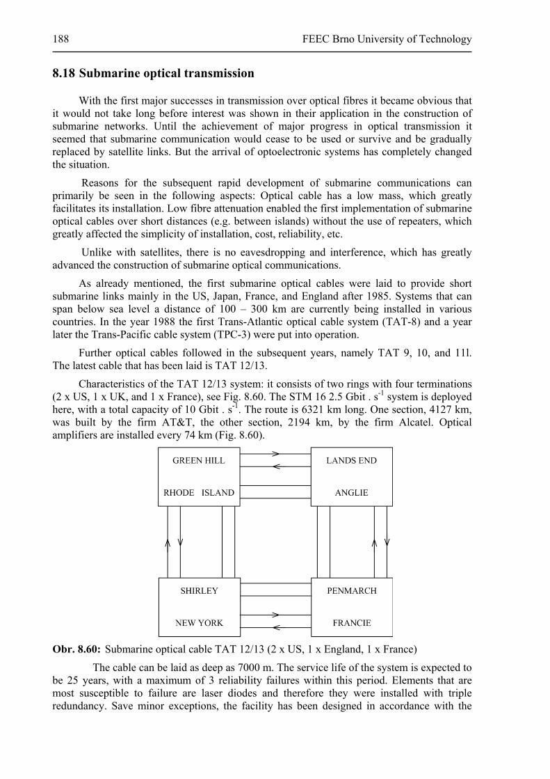
188 FEEC Brno University of Technology
8.18 Submarine optical transmission
With the first major successes in transmission over optical fibres it became obvious that it would not take long before interest was shown in their application in the construction of submarine networks. Until the achievement of major progress in optical transmission it seemed that submarine communication would cease to be used or survive and be gradually replaced by satellite links. But the arrival of optoelectronic systems has completely changed the situation.
Reasons for the subsequent rapid development of submarine communications can primarily be seen in the following aspects: Optical cable has a low mass, which greatly facilitates its installation. Low fibre attenuation enabled the first implementation of submarine optical cables over short distances (e.g. between islands) without the use of repeaters, which greatly affected the simplicity of installation, cost, reliability, etc.
Unlike with satellites, there is no eavesdropping and interference, which has greatly advanced the construction of submarine optical communications.
As already mentioned, the first submarine optical cables were laid to provide short submarine links mainly in the US, Japan, France, and England after 1985. Systems that can span below sea level a distance of 100 – 300 km are currently being installed in various countries. In the year 1988 the first Trans-Atlantic optical cable system (TAT-8) and a year later the Trans-Pacific cable system (TPC-3) were put into operation.
Further optical cables followed in the subsequent years, namely TAT 9, 10, and 11l. The latest cable that has been laid is TAT 12/13.
Characteristics of the TAT 12/13 system: it consists of two rings with four terminations (2 x US, 1 x UK, and 1 x France), see Fig. 8.60. The STM 16 2.5 Gbit . s-1 system is deployed here, with a total capacity of 10 Gbit . s-1. The route is 6321 km long. One section, 4127 km, was built by the firm AT&T, the other section, 2194 km, by the firm Alcatel. Optical amplifiers are installed every 74 km (Fig. 8.60).
Obr. 8.60: Submarine optical cable TAT 12/13 (2 x US, 1 x England, 1 x France)
The cable can be laid as deep as 7000 m. The service life of the system is expected to be 25 years, with a maximum of 3 reliability failures within this period. Elements that are most susceptible to failure are laser diodes and therefore they were installed with triple redundancy. Save minor exceptions, the facility has been designed in accordance with the

Optoelectronics for telecommunications and informatics 189
respective ITU-T recommendations. As a result, similar facilities could be built in the US, France and UK, which can communicate with one another. The system has its own check and failure modes.
Submarine optical cable TPC 5 interconnects the US, Japan, and Hawaii. FLAG (Fiberoptic Link Around the Globe), a cable-optic system of over 27 000 km in length, interconnects the UK, Egypt, India, Thailand, Hong Kong, China, Korea, and Japan.
The latest major achievement is the AFRICA TWO optical network interconnecting 40 countries around the African continent, length over 40 000 km.
Optical fibres for submarine cables undergo special testing. The design of the cable is more or less classical; optical fibres are in the centre of cable core (mostly in tubes or chambers), after which there is the protective tube (Cu, Al), and then the strength and protection elements. The cable diameter ranges between 20 and 50 mm. Cable manufacturers can deliver cables in runs equal to repeater section lengths, i.e. about 70 km.
8.19 Installation of optical routes
The same as with “classical” transmission systems, the installation of an optoelectronic transmission facility can be divided into the indoor (exchange) part and the outdoor (cable) part.
As regards the indoor installation of optical link termination, this is essentially a matter of providing the rack with blocks (cassettes). The optical transmitting element (the same as the receiving element) has its output connected via fibre directly to the connector. A direct connection to the optical distribution box is thus made possible. The optical distribution box (provided it is deployed) is used to terminate the optical cable and distribute the individual fibres to the respective optical link terminations.
The construction of the outdoor part will now be dealt with in detail. What is concerned here is the interconnection of two terminal devices by a cable. Optical cable (similar to the metallic one) can be laid in the following mediums: air, earth, cable duct, conduit (tunnel), cable trench (pipes), water, residential and industrial buildings.
Conditions for laying the cable may be quite different even within the individual mediums. Extreme conditions are therefore always considered in which the cable will be operated without changes in transmission parameters. Each of the above mediums offers specific possibilities of cable damage. For example, a cable laid in earth can be damaged by extreme temperature changes, severe frost causing soil movement, vicinity of hot springs, presence of oil, animals, earthquakes, landslides, and other circumstances.
In the case of overhead lines some of the above factors need to be considered but, in addition, also wind, rain, snow, ice, sunshine, falling stones, birds, and insects.
All the factors given above are of natural character. But there are also artificial factors, where we include the effects of fire and smoke, road transport, action of oil and vapours, building activities, and vandalism.
It is therefore evident that the cable should resist all these effects and this may be helped by suitable cable-laying and selection of the route.
The very laying and handling of optical cable can be of minimal or small but also severe effects on transmission parameters. Impairment may stem from bending the fibre, fibre microbends, fibre deformation, and admission of moisture. The ideal state would be if the

190 FEEC Brno University of Technology
optical fibre in the installed cable had the same properties as the individual fibres before being twisted to form the cable core in the factory.
The above fibre microbends are a failure caused by normal forces acting on the cable. The longitudinal axis of the fibre is not straight, it is wavy. The deviation of the actual axis from the ideal one is usually ca. 1 μm and the period of axis ripple is in millimetres to centimetres. Normal forces acting along the fibre can arise during manufacturing but also, not infrequently, during cable laying or due to changes in cable dimension caused by temperature fluctuation. The problem with temperature appeared, for example, in the Czechoslovak optical cable (at extreme negative temperatures). Susceptibility to microbending also depends on the refractive index difference between the core and the jacket, and also on the diameters of the optical fibre core and jacket.
In the case of fibre (cable) bends, optical losses increase from certain limits onwards. There is also a danger that cracks will eventually appear in the fibre, leading to its rupture. In the course of bending, longitudinal forces appear in the fibre, and normal forces also act on it.
An even higher degree of fibre degradation is its deformation, no matter whether due to twisting, bending, handling, stressing, etc.
Moisture also reduces the tensile strength of fibre and cuts the time to static failure. Increased optical losses can be the consequence. In winter, cable moisture may freeze up and make the fibre break.
Protecting the fibre against moisture is difficult because filler materials are not fully impermeable. The following measures are therefore taken, either separately or in combination:
- protection by air pressure, - barrier against moisture, - filler material.
All the above factors need to be considered when selecting the cable route and when laying the cable.
While being laid, the cable is exposed, for a short-time, to high tensile stress. It is important not to exceed the tensile force limit as declared by the manufacturer; otherwise the fibres will start cracking. The cable is manufactured in very long runs (1000 – 2500 m, sometimes 10 000 m) and thus it is opportune to use such a laying technology that the runs do not need to be cut. When pulling the optical cable in, it is necessary to use an automatic power-cutting device (dynamometer), which will stop the pulling procedure when the tensile force increases.
Currently the most frequently used method is blowing the optical cables by air pressure into HDPE protection tubes. The cable is thus better protected against external effects and damage. In the case of failure, the damaged run is easy to replace. The principle consists in the cable being borne by air pressure. In Italy, for example, they have cables borne by water. Depending on the terrain, 2 to 6 km (maximum 10 km) of cable can be blown in (for longer runs, a tandem blower must be used).
In towns, cable ducts are used for laying cables in order to avoid frequent digging up of pavements and roads. The ducts are made up of pipes, into which the HDPE tube is pulled, and the optical cable goes into the latter. In recent years, cable ducts (multichannels) by the SITEL company have proved to be good (Fig. 8.61).
All types of cable can be laid in multichannels (four-, six- or nine-way ducts). The system is designed for the dry process of construction, without the necessity of using

Optoelectronics for telecommunications and informatics 191
concrete, and it can be used for the construction of both subsurface and deep-buried cable ducts. Square cross-sections enable cables to be pulled in faster and more easily thanks to lower friction forces acting on the cable itself. The whole system is installed section by section, with individual splices being sealed with rubber packing and locked by four elastic steel clips.
The basic features of this technology include: materials stability and robustness, potentially high concentration of cables in a small space, speed of installation, possibility of parallel installation, and reduction of piping to individual tubes.
Obr. 8.61: Multichannels (cable duct)
Apart from these classical methods of laying the cable, some “novelties” have come to be used.
MCS (Micro Cabling System) method
Micro cabling systems NSC are an expedient alternative to laying and installing optical cables and optical cable joints in the construction of new access networks. Optical cables designed for these systems are laid in roads or pavements (MCS-Road) or in sewage drains (MSC-Drain). The MSC-Road and MSC-Drain micro cabling systems are mutually compatible and also compatible with the existing conventional optical cable networks.
MSC-Road Micro Cabling System
This is a system of special micro cables, which are made up of a thick-walled copper tube with optical fibres; the tube is protected by polyethylene (PE) jacket, see Fig. 8.62.
Obr. 8.62: Optical cable in MSC-Road version
Outside diameter of micro-cables is 7 mm (for a maximum of 60 optical fibres) or ca. 9.6 mm (for a maximum of 120 fibres). Micro-cables contain 2, 24, 26, 48, 60 or 144 optical fibres. Individual fibres are identified by their colour marking.
For optical micro-cables to satisfy the parameters declared by the manufacturer it is necessary to respect the minimum admissible radius of micro-cable bending (ca. 70 mm) and the maximum admissible tensile force (1 000 N). For the splicing of optical micro-cables, underground waterproof cable joints of the type of U-60 and U-144 were developed; they are

192 FEEC Brno University of Technology
made of stainless steel and placed in roads, pavements, etc. These cable joints can resist heavy loads. The two types of cable joints enable straight (continuous) joining of optical micro-cables to a maximum capacity of 60 fibres (U-60) or 144 fibres (U-144).
In the installation, the optical micro-cable is laid in a groove milled in the road, pavement or another type of surface. The depth is chosen between 60 and 120 mm. After milling (cutting, grinding) the groove, it is cleaned and dried, e.g. by hot air blown into the groove under pressure. The optical micro-cable is placed in the groove and, using a thrust ring, it is pressed to the groove bottom. A cord of foam polyethylene (functioning as filler material and thermal insulator) and then a cord of foam rubber (functioning as a thrust element) are pressed onto the micro-cable in the groove. Eventually, the groove is filled with a suitable sealing compound.
The above is a Siemens patented system. It is suitable for installation in high-quality roads, in large-area facilities, where up to 1 km of cable can be laid in a day (excavation work not included) [8-18].
MCS-Drain Micro-Cabling System
This special optical micro-cable is formed by a thick-walled aluminium tube with optical fibres, armoured with a continuous layer of steel wires. This armouring arrests the tensile forces and protects the cable against rodents. There is a polyethylene (PE) jacket over the armouring. Outside diameter of the aluminium tube is about 6 mm, the diameter of the whole cable (including PE jacket) is ca. 10.6 mm. For the optical micro-cables to satisfy the parameters declared by the manufacturer it is necessary to respect the minimum admissible radius of micro-cable bending (ca. 100 mm) and the maximum admissible tensile force (1 500 N).
In the installation, the optical cable is laid in sewage drains, which are first cleaned with water under high pressure. After cleaning, the optical cable is smoothly pulled into the drains, where it is fixed in the upper part of the piping.
Overhead optical cables
In the course of constructing optical routes, it is sometimes necessary to mount the cables on poles. This is done using self-supporting cables or bearer wires. Spacing between poles must be chosen such that the cable is not exposed to tensile stress beyond admissible limit. Ice accretion, wind and temperature changes must be considered in this choice. The line must be suitably anchored to prevent any motion of the poles. It is a good practice to locate the optical cable at the top of the pole because there it is best protected against damage during line maintenance. If there is a danger that the jacket might be damaged by rodents, the cable must be armoured.
The choice of a suitable method for stretching the cable is also important. During installation, attention must be paid to keeping the minimum radius of bending. It is recommended to suspend the cable from a bearer wire that has been stretched in advance.
Underwater cable laying
Another possibility of laying cables is underwater laying. The cable is laid under or on the bed of creeks, rivers, lakes or shallow waters. The cables can be installed loose in trenches or in pipes or they can be laid from ships as floating cables. In most cases they are mechanically covered. The cables are armoured to be additionally protected against the river stream and their waterproofness is usually increased by the filling material. Cables laid in waters where fishing is practised need double armouring.
Optoelectronics for telecommunications and informatics 193
Application of microtubes
This is the latest trend in the construction of optical networks of the type of FTTH, when a PE microtube is brought to the subscriber, into which one or two optical fibres are then blown. Fibres can be blown to a distance of 2 to 6 km. Cable joints and directional couplers for micro tubes have been worked out.
When the respective runs have been installed in the proper places, their splicing can start.
The splicing of optical fibres was dealt with in detail in Chapter 5.
The methods for splicing optical cable jackets are based on the usual methods of splicing metallic cable jackets. The cable joint must:
- restore the integrity of cable jacket, inclusive of the mechanical continuity of the strength member,
- protect spliced optical fibres against the effects of cable environment, - provide appropriate conditions for housing the spliced fibres and their reserves.
In keeping with the criteria for the splicing of cables with plastic jackets, it will hold for optical cables:
- the sleeve material must be compatible with the jacket material, and the temperature used in splicing should not fundamentally affect the physical structure of the plastics, metals, and glues used,
- the proposed technologies must enable laying the cables in earth, swamp or an available cable chamber,
- it must be possible to use the technology in heat, frost and moisture, - the method must allow opening the cable joint and closing it again without
interrupting the links in operation, - the cable joint must be robust as regards mechanical effects, - economic criteria need to be taken into consideration too.
Fibres in the cable joint are arranged in such a way that fibre reserve is located in the fibre space for possible repairs and adaptations in the cable joint. Already in the process of installation it is in most cases necessary to repeat fibre splicing until the required splice attenuation is obtained. The radius of the laid fibre must be small with respect to the cable joint dimensions but not so small that the fibre should be damaged due to static fatigue. This necessarily leads to specific requirements for laying the fibre in the cable joint cavity. The methods of implementation differ depending on the cable joint design and number of fibres.
The splicing of optical cable jackets is based on the application of contractible thermoplastic materials. The sleeve can be made of this material in the form of tube, longitudinally combined tube or strip. The internal side of the sleeve and strip can be coated with a material which melts under heat and thus a waterproof closure is obtained between the contracted sleeve and the cable jacket.
The quality of cable joints is evaluated in order to assess their resistance to failure in the given medium. This resistance is usually examined by testing. The respective tests fall into three basic groups:
Mechanical requirements
- cable joint resistance to pressure, - cable joint resistance to impact, - resistance to tension, - resistance to bending in sleeve neck,
194 FEEC Brno University of Technology
- resistance to vibrations. Electrical requirements - resistance to induced (short-circuit) voltages, - electrical capacitance. Environmental effects - cyclic temperature changes, - immersion of cable joint in water, - resistance to chemicals, - resistance to fungi and blight, - resistance to overpressure in the cable joint.
The programme of testing should cover the whole range of manufactured cable joint sizes and configurations.
The basic cable section usually includes several manufacturing runs. When determining the transmission parameters of a section it is necessary to take into consideration not only the properties of the cable runs used but (in addition to other factors) also the effect of splices and connectors, and the effect of the coupling of modes that affect the bandwidth and attenuation size.
The transmission properties of manufacturing runs, splices and connectors have a certain occurrence probability, which often needs to be taken into consideration with a view to an economic design of the route.
Attenuation of the basic cable section is given by the sum m
n n s c.a L a x a y, (8.22)
where n is the attenuation coefficient of n-th fibre, Ln is the length of n-th fibre, m is the total number of fibres, as is the average splice attenuation, x is the number of splices in the section, ac is the average connector attenuation, and y is the number of connectors.
The values an, as and ac can be obtained as average values or they can be calculated using the standard deviation.
Two approaches can be used to form the basic cable section:
1. To select fibres from one category given for the manufacturing runs and assume the highest value of the selected category.
2. To select fibres from various categories on condition that attenuation of the basic section will not exceed the required attenuation. In that case the real attenuation coefficient is equal to the attenuation coefficient of n-th fibre.
From the practical viewpoint it is necessary to maintain certain reserve attenuation for potential additional splices and cable branching devices, for losses due to aging and temperature changes. For losses in splices and connectors the average value is considered. In the design of concrete routes it is necessary to take into consideration statistical changes of these parameters.
When the cable has been laid and is connected at both ends to optical link terminations, it is possible to address the final measurements.

Optoelectronics for telecommunications and informatics 195
Results of the measurement of link routes must correspond to the respective technical conditions and recommendations of ITU-T. Also, the stability of the values measured and the overall reliability of the system must be proved.
The most widely monitored route parameters include the sensitivity of optical receivers (in loop operation), measurement of bandwidth, measurement of attenuation, and measurement of error rate.
Detection (search for) optical cables
Metallic pair can be embedded in the core (or jacket) of optical fibre to enable measuring the cable insulation state and detection of a buried cable. But many cables are fully dielectric and then there are difficulties with the detection of the buried cable.
For this reason, markers are added to the cable after certain distances. The markers are easy to identify by a locator and the cable can be traced. The location and depth of the cable can be established with very high precision.
Cable systems
This group covers mechanical technologies for the splicing and termination of optical cables.
Optical cable joint (splicing module), type 2500LG, is a separate optical cable joint for universal application. Its cover is made of reinforced thermoplastic material, which provides the cable joint with very good mechanical, climatic, and chemical protection. In the basic version, the cable joint is provided with three cassettes for storing fused or mechanical splices of optical fibres. Equipped with the cassettes, the cable joint has a capacity of 24 fibre splices (fused or mechanical). An additional extension cassette D-182563 can be included in the cable joint. From among the available cassettes, 3 cassettes of the type UC-54 can be located in the cable joint. These cassettes enable extending the cable joint capacity up to 54 fused splices while using the mechanical sandwich protection of splices. The basic splice package contains all the components necessary for installing two cables (o.d. 10 ÷ 21.6 mm) into the main cable joint inputs. The only consumable that needs to be ordered for cable joint installation separately is the filler material, so-called encapsulant, which is used to fill up the cable joint and which prevents water from penetrating into the inner space of the cable joint (see Fig. 8.63).
Basic properties and features:
- universal application, - capacity 24 optical fibre splices, with extension cassettes up to 30 or 54 splices, - possible application of: mechanical fibre splices, fused fibre splices with thermally
contractible protection of splices, fused fibre splices with mechanical sandwich protection of splices.
Type 3000 optical cable joint can hold up to four such cassettes (36 splices each), with a
resultant capacity of 144 fibre splices.

196 FEEC Brno University of Technology
Obr. 8.63: Optical splicing module
Optical distribution boxes, LGX series
Optical distribution boxes of the LGX series are designed to terminate or interconnect optical cables inside buildings. Together with accessories, optical distribution boxes form a modular, easy-to-extend unit. They can be placed in 19”, 21” (ETSI) or 23” racks or they can be fixed directly on a wall. The basis of LGX series is formed by individual racks. By their function, the racks fall into:
- termination racks – are used to terminate fibres on connectors, - storage racks for splices – are used to store fused fibre splices and their reserves, either
when fusing pigtails or when directly fusing fibres from different cables, - storage boxes for connection modules – are used to store redundant runs, - optical connection modules, - combination racks – serve as a combination of storage and termination racks.
Racks thus enable the fusing of pigtails and their termination on connector panels. The capacity of individual boxes can be 24, 72 or 144 fibres. The boxes are 43.2 cm (17”) wide and 27.9 cm (11”) deep. The height differs from type to type, and it ranges from 12.7 cm (5”) to 53.4 cm (21”).
Some distribution boxes are installed in the Laboratory for transmission media (see Fig. 8.64).
Obr. 8.64: Optical distribution boxes

Optoelectronics for telecommunications and informatics 197
8.20 Free-space optical communication
Free-space optical links are implemented as links in closed spaces, free space (the atmosphere), and outer space.
Free-space optical links in closed spaces are implemented via optical fibreless modems (two-point modems or with connection to LON, etc.), which make servicing much more comfortable. Transmission to headphones is possible, e.g. TV sound accompaniment or in facilities for video-conferencing or interpreting. This area also includes wireless telephony, remote control of TV sets, and supervision and control of other devices. In all these cases the transmission is of high quality and without interference; in the case of interpretation facility there is the added advantage that eavesdropping outside the room is impossible (in contrast to similar electromagnetic facilities). IR radiation cannot get out of a closed space. Energy transmission between the transmitter and the receiver can proceed:
- directly, by directional radiation, - indirectly, by diffuse radiation (e.g. be reflection from wall surfaces).
Directional radiation is made use of when establishing point-to-point links. Diffuse radiation is used to establish connection among several terminals.
In the transmission using IR radiation a sufficiently strong field must be created in the closed space with receivers. High-quality transmission is conditional on uniform and sufficient radiation. The required optical emitted power is of the order of units to tens of watts. In large spaces it is advisable to have decentralized radiation, i.e. to use a greater number of radiators and these should be located as high as possible. It is good practical experience to install radiators close to the ceiling and tilt them into the space.
Directional radiation
Radiant energy propagates from the source of radiation in all directions at the velocity of light c; radiant energy crossing a surface per unit time is called radiant flux through surface. Radiant flux Pe gives the power transmitted by IR radiation and is measured in watts.
Radiant intensity Ie of a point source in a certain direction from this source is taken to mean the differential ratio of radiant flux Pe, which emanates from the source in this direction into a small solid angle Ω, and this solid angle
1ee W . s r .
d PI
d
(8.23)
Radiant intensity Ee gives the differential ratio of radiant flux Pe incident on an elementary part of an area A to the size of this area
2ee W . m ,
d PE
d A (8.24)
where
2 1 1 2 2e e o2
cos cosd . ,
d A d AP L
r
(8.25)
Le is the radiation (W s r-1 m-2),
d A1 is the element of transmitter surface (m2),
d A2 is the element of receiver surface (m2),
ε1 is the radiation angle of transmitter,

198 FEEC Brno University of Technology
ε2 is the radiation angle of receiver,
r is the distance between transmitter and receiver (m),
Ωo is s r.
The intensity of the radiation incident on an area from isotropic point source changes, by the cosine law, with radiation direction deviation ε from the normal to this area and with the square of distance r
.cos2e
e r
IE (8.26)
In the case that the area of receiver inlet opening is larger than the area formed by the radiant beam, it holds that the intensity of radiation incident on the receiver decreases with the square of distance r
e 2
1.E
r (8.27)
The passing beam of radiant intensity Ee is further reduced by energy dE per distance dx
e
e
dx.d E
kE
(8.28)
By solving differential equation (8.28) for initial and boundary conditions we obtain relation (8.29), which gives the losses due to absorption by environment along the whole distance r between the transmitter and the receiver
-kre O e .E E (8.29)
Since in practice we will never achieve a situation that the area of inlet opening of receiver A is at least equal to the beam trace A1 (A1 > A), the energy losses due to the difference between inlet opening area of receiver and beam trace area will be expressed by the ratio of these areas
.1A
A (8.30)
The quality of reflection areas of receiver and transmitter (if used) are expressed by reflectance coefficients ρp and ρv, with ρp and ρv < 1. After substituting we obtain the expression for energy incident on receiver in directional radiation
-kr
e O p v 2
e. ,
rE E (8.31)
where Ee is the energy incident on receiver (W),
EO is the transmitted energy (W), 1
1. AA ,
A is the area of receiver inlet opening (m2), A1 is the area of transmitter beam trace (m2), p is the reflectance coefficient of receiver area, v is the reflectance coefficient of transmitter area k is the extinction coefficient = 3,90 . 10-4 m-1 (for λ = 0,9μm), r is the distance (m).

Optoelectronics for telecommunications and informatics 199
These relations can be used when solving problems of information transmission using sharply directed IR radiation over large distances. In transmissions in closed spaces the atmosphere attenuation can be neglected since it has been established that attenuation in the range of currently used wavelengths does not exceed the value 0.6%, even in the case of 100% humidity [8.21].
Diffuse radiation
The total power of IR radiation depends to a considerable degree on the room dimensions and the material of surfaces. The higher the reflectance coefficient of material surface ρ, the lower the necessary IR radiant power is. The reflectance coefficient ρ is a function of incidence angle α, wavelength λ and polarization p, i.e. ρ = f (α, λ and p). The reflectance coefficient decreases with increasing incidence angle. Typical values for the region of the 1st window:
- white wall 0.75 – 0.85, - red wall 0.40 – 0.50, - blue wall 0.05 – 0.20, - black wall 0.01, - white paper 0.80 – 0.85, - black velvet 0.005, - white wood 0.35 – 0.50, - dark wood 0.10 – 0.20
Let us assume that the reflectance coefficient of all the surfaces that delineate the given
space is the same, equal to ρ, and that in time Δt, which is the average time of wave propagation on the path between the radiator and the reflection surface of reflectance ρ, average power Pstr is emitted. After the first reflection, part of the emitted power, which is equal to ρ Pstr, remains inside the space. At the instant of second reflection 2Δt the power has the value Pstr + ρ Pstr and therefore power P2 inside the space has the value P2 = ρ (Pstr + ρ Pstr). At the instant of k-th reflection kΔt the power inside the space is
2 kk stř stř stř stř .P P P P P (8.32)
Since the reflectance coefficient is 0 < ρ < 1, we can write
střk .
(1 )
PP
(8.33)
In a closed space volume the state of equilibrium occurs: power emitted from the radiator will compensate the absorption by delineating surfaces. The average IR radiation inside the closed space will be 1/(1-ρ) times greater than emitted power.
If several different materials of different reflectance coefficients are used inside a closed space (which is often the case in practice), then it is necessary in relation (8.33) to substitute for the value of reflectance coefficient ρ the average value ρ of all the inner surfaces. This value is calculated from the relation
1 1 2 2 n n
1 2 n
,A A A
A A A
(8.34)
where n21, AAA are the areas of individual surfaces,
1, 2 n are the reflectance coefficients of individual surfaces.

200 FEEC Brno University of Technology
It will be proved in the following that in the transmission via IR radiation the closed space behaves as an inertia element, which eventually turns out to be a limiting factor of the whole transmission system. The radiation velocity is finite. Information transmission is made possible by changing an arbitrary parameter of radiation. Technically the simplest thing is to modulate the intensity of radiant flux, which means that the instantaneous emitted power Po is a function of time. It is obvious that in time t + dt the instantaneous power Po will already have a different value and all the preceding signals, which after multiple reflections strike the receiver at this instant (t + dt), will show as disturbance signals.
Let us assume that in an arbitrary system for information transmission inside a closed space by means of IR radiation there is attenuation, which is caused by m reflections, with the m-th reflection not representing the disturbance value of reception. The attenuation is the result of k-th reflection, after which the value of radiant power in a closed volume equals
kOO ,
PP
m (8.35)
where
.0,0log1log
log
k
mk
Let the period of modulation frequency of transmission system be equal to T. In time T there will be
t
Tk
(8.36)
reflections. The average time of wave propagation in a closed volume is tied by the geometrical dimensions of the closed space by the mutual relation
4,
Vt
c A (8.37)
where V is the volume of the room (m3),
A is the total area of surfaces delineating the given volume (m2),
c is the velocity of light propagation in vacuum (m . s-1),
substituting (8.35) and (8.36) and solving (8.37) for Tf 1max we obtain
max
. logHz .
4 . log
c Af
V m
(8.38)
This relation enables determining the maximum carrier frequency for single- and multi-channel systems of information transmission by means of IR radiation inside a closed space [8-22].
From relation (8.38) it is also evident that the highest carrier frequency is largely affected by the closed space dimensions, more exactly by the ratio of the room surface to the room volume.
Another factor that influences the result is the reflectance coefficient of all surfaces inside a closed space. The actual number of reflections m inside a closed space is difficult to establish but it can be assumed to range between 100 and 100 000. With increasing reflectance coefficient ρ the number of reflections increases, and vice versa.

Optoelectronics for telecommunications and informatics 201
Modulation of optical radiation
For optical transmitters in the 0.8 to 0.9 μm wavelength range LED diodes with direct modulation of the modulation signal are used. Emitted radiation does not propagate evenly over the whole space; most energy is emitted in the direction of optical axis, i.e. the straight line normal to the chip plane or passing through its centre. An idea of the distribution of radiant energy can be obtained from the radiation characteristics. For practical purposes it is of advantage to determine the graphic dependence of output optical power on the distance from the source and on the angle (from the optical axis), as shown in Fig. 8.65.
Obr. 8.65: Power vs. distance curves for free-space transmission
To obtain higher radiant powers several LED diodes are placed in one plane, which forms the so-called radiator. The number of diodes in the radiator can be 6, 12 or even much more.
For example, a radiator for monophonic and stereophonic transmission of signals can be set up, for example TV sound accompaniment in flats. The radiator can have six LEDs with cooler and reflector on each diode.
The power radiator is formed by 12 IR LEDs with cooler and reflector. The total emitted power is 200 mW, which guarantees good reception within ca. 15 m. The radiation characteristic of radiator is given in Fig. 8.66.

202 FEEC Brno University of Technology
Obr. 8.66: Radioation characteristic of radiator
For transmissions over greater distances (also in the case of a higher number of channels) an even higher power is necessary. For example, a radiator with 167 LEDs can be used, whose radiation angle is 60º.
Obr. 8.67: Diffuse coverage: a) in a meeting room, b) around a table
For the detection of radiation a silicon-based PIN photodiode is usually used, whose characteristic has sensitivity on the same wavelength as that of the above radiation source.
In the design it is necessary to take into account also potential reception disturbance due to light sources in the room (fluorescent lamp, etc.). In all such cases simple filters are used, which filter the undesirable radiation components (simple filters such as film, special glass, etc.). Without filtering, an increase in noise of up to 50% can appear in some bands.
The frequently used modulation methods include FM modulation and FSK modulation. In many devices the PSK-IM modulation is used.
For the diffuse coverage of a space it is necessary to place a radiator in each corner as close to the ceiling as possible and to tilt them under 20º - 40º into the space. Radiators must
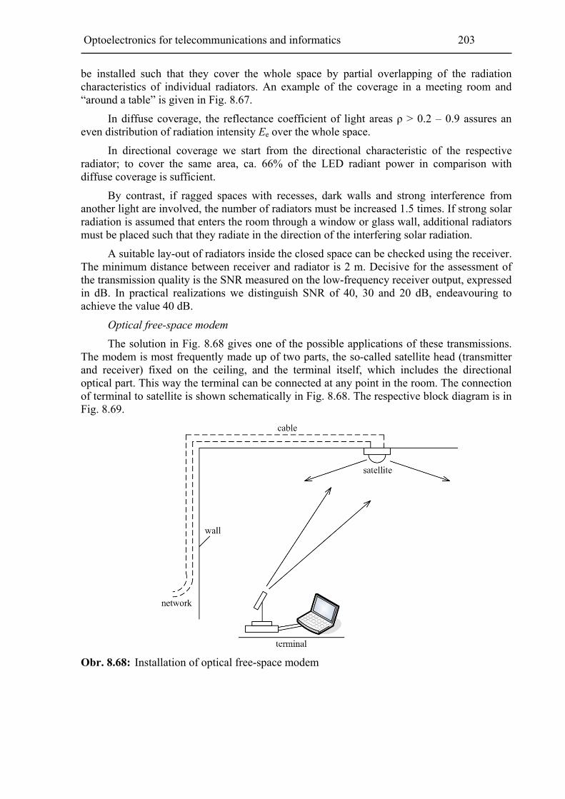
Optoelectronics for telecommunications and informatics 203
be installed such that they cover the whole space by partial overlapping of the radiation characteristics of individual radiators. An example of the coverage in a meeting room and “around a table” is given in Fig. 8.67.
In diffuse coverage, the reflectance coefficient of light areas ρ > 0.2 – 0.9 assures an even distribution of radiation intensity Ee over the whole space.
In directional coverage we start from the directional characteristic of the respective radiator; to cover the same area, ca. 66% of the LED radiant power in comparison with diffuse coverage is sufficient.
By contrast, if ragged spaces with recesses, dark walls and strong interference from another light are involved, the number of radiators must be increased 1.5 times. If strong solar radiation is assumed that enters the room through a window or glass wall, additional radiators must be placed such that they radiate in the direction of the interfering solar radiation.
A suitable lay-out of radiators inside the closed space can be checked using the receiver. The minimum distance between receiver and radiator is 2 m. Decisive for the assessment of the transmission quality is the SNR measured on the low-frequency receiver output, expressed in dB. In practical realizations we distinguish SNR of 40, 30 and 20 dB, endeavouring to achieve the value 40 dB.
Optical free-space modem
The solution in Fig. 8.68 gives one of the possible applications of these transmissions. The modem is most frequently made up of two parts, the so-called satellite head (transmitter and receiver) fixed on the ceiling, and the terminal itself, which includes the directional optical part. This way the terminal can be connected at any point in the room. The connection of terminal to satellite is shown schematically in Fig. 8.68. The respective block diagram is in Fig. 8.69.
Obr. 8.68: Installation of optical free-space modem

204 FEEC Brno University of Technology
Obr. 8.69: Block diagram of optical transmission
In practical implementations, diffuse radiation with a range of over 10 km is used. The devices achieve 100 Mbit . s-1 transmission speeds. The type of modulation used is FSK-IM (PSK-IM). The radiation sources are usually LED diodes of the wavelength λ = 0.88 μm, and PIN PD detectors. The modem operates in half- or full-duplex. An approximate direction-adjustment of the facility is made for the terminal – satellite transmission.
Optical free-space links in free space
These links are designed, above all, for rapidly establishing communication without the necessity of laying cables. These links are ”line-of-sight” links, i.e. highly directional and, in comparison with radio links their operation is not conditional on frequency allocation by CTU. Using these links, it is no problem to span roads, valleys, etc. The disadvantages of these links include the difficulty of bringing transmitter into phase with receiver, and the not always 100% reliability of the links, which depends on fog, flying flocks of birds, etc. Development in this area is focused on seeking methods that increase the resistance of transmission to atmospheric events [8.23].
This kind of transmission is currently implemented by the laser beam, with the optical power divided among several parallel beams for the sake of increased reliability.
Transmissions are most frequently realized at speeds of 155 Mbit . s-1 over distances from hundreds of metres to 1.2 to 3 km. The wavelengths used are 785 nm, 850 nm, and 1550 nm. Wavelength multiplexers with speeds of up to 10 Gbit . s-1 have already been installed.
The total link attenuation between the transmitter and receiver can be expressed by the relation
dBpatm12vc aaaaa (8.39)
where av is the attenuation in transmitter system,
Optoelectronics for telecommunications and informatics 205
a12 is the attenuation by propagation,
aatm is the attenuation due to atmospheric phenomena,
ap is the attenuation due to receiver system.
Attenuation due to propagation a12 is given by the ratio of optical intensities on the beam axis at the receiver and transmitter sites. In the remote radiation zone the divergent Gaussian beam can be approximated by spherical wave. For attenuation due to propagation the following relation can be derived
dBlog2012O
O12 LL
La
(8.40)
where LO is the so-called auxiliary length.
To be able to express LO the diameter of optical transmitter system DTXA and the planar angular width of transmitted beam φ1 must be known. The two quantities are obtained by measuring.
Atmospheric attenuation aatm is divided into two components: constant attenuation, i.e. attenuation in the “pure” atmosphere, and random additive attenuation of the real atmosphere.
In the power balance in free-space links it is necessary, the same as in fibre links, to consider the reserve, error rate, signal-to-noise ratio, and, in addition, short-time fading, and wave interference in turbulent atmosphere. Certain problems arise with vibrations of fixing brackets and when these links are deployed in new buildings, which may have the tendency to “slide” (before they “settle”), etc.
It is obvious that not all of the negative effects will come about at the same time and everywhere. Id depends on the respective localities, buildings, and flocks of birds flying above the town centre, etc.
These facilities are offered by many firms under firm names such as CANON –ANOBEM, CBL-Laser Link, SONA-SONA beam. The current top product in this area is Tere Scope 10GE (10 Gigabit Ethernet) of the MRV Company, with an operation range of up to 850 m. Those interested can find more details on the respective web pages.
8.21 Optical filters
Filters change the spectral distribution of the energy of emitted radiation or they almost evenly weaken the radiation in a certain, relatively broad region of the spectrum. The effect of filters is characterized by the coefficient of spectral transmissivity τ(λ) as a function of the wavelength of emitted radiation according to the relation
1 , (8.41)
where
e
?!e (8.42)
is the spectral coefficient of reflectance, and
and
e
e (8.43)
206 FEEC Brno University of Technology
is the spectral coefficient of absorption.
By the law of energy conservation the sum of reflected, absorption and passed radiation must be equal to incident energy. It must therefore hold
.1i (8.44)
Let us finally define the coefficient of spectral transmissivity τ(λ) by the relation
,e
e
(8.45)
which describes the filter transmissivity for radiation: for example, the value τ(500 nm) = 0.7 means that radiation of wavelength 500 nm is absorption- and reflection-weakened by 30% during throughput. The spectral coefficient of own transmissivity is
vste
výste
i
(8.46)
and the coefficient of own absorption αi(λ)
eλ eλvst výst
ieλ vst
,
(8.47)
where we relate the output or absorbed radiant flux to the input flux and not to the total incident radiation.
In view of the above, the function τ(λ) can be determined either using α(λ) (so-called absorption filters) or using ρ(λ) (so-called interference filters). Using low-absorption interference filters the so-called colour dividers can be designed.
The region of wavelength of incident radiation is divided into a part through which radiation has passed and a part with reflected radiation. From the viewpoint of radiation receiver it is most important that at the output of optical radiation receiver the ratio of radiator signal to the signal of noisy background should be as large as possible.
The need for filtering was mentioned in connection with information transmissions inside closed spaces, where the matter in question was to filter the undesirable disturbance components of daylight and lighting. This problem is relatively easy to solve using an optical high-pass filter (the above disturbance components are in lower wavelengths). The application in multiplex systems requires a more challenging solution using interference filters.
Undesirable disturbing light can today be filtered directly, using commercial photodiodes with embedded optical filters. Optical filters made of coloured glass achieve a high degree of throughput, e.g. filter RG 700: 1% at λ = 750 nm, 80% at λ = 800 nm, and 97% at λ = 860 nm; filter RG 850: 1% at λ = 820 nm, 80% at λ = 870 nm, and 97% at λ = 920 nm.
Optical filters can be used to implement filters of the type of low-pass, high-pass, band-pass, and notch filter, just like in electrical technology.
It is even possible to make use of the favourable properties of optoelectronic elements when, for example, a combination of optical high-pass filter and a photodiode behaves as an optical pass-band filter with cut-off frequencies λmez1 and λmez2.
In some simple applications it has been found of advantage (also because of availability) to use a non-exposed but developed reversal film (Agfa CT 18, Fomachrom D 18). Using such films, the interference caused by fluorescent lamp can be limited and the effect of daylight strongly reduced.

Optoelectronics for telecommunications and informatics 207
In practical implementations using high-quality filters (coloured glass) the signal-to-noise ratio is often reduced by more than 15 dB.
There are also filters on the basis of phototropic glass, in which the throughput coefficient is reduced via short-time radiation. They begin to find application as optical memories in data processing. They are also frequently used as adaptive grey filters in sunglasses.
Dispersion filters can also be used for the purpose of filtering, when the decomposition is performed by prism or optical grating. When the prism is used, optical losses are 5 – 7 dB (but the cost is high and mass production difficult).
Optical gratings are of much promise; their optical losses are ca. 2 – 4 dB, the cost is low and mass production relatively easy.
Absorption filters
Material used for absorption filters is, above all, suitable coloured glass. While the effect of a specific filter on radiation is described by the coefficient τ(λ), to calculate the transmissivity for various filter thicknesses we need the coefficient τi(λ). It holds τi(λ) > τ(λ) since the coefficient τi(λ) does not include reflection losses. In the filter calculation the following relation is sufficient
.21 xi (8.48)
where x is the coefficient of surface reflectance given by the relation
2
x´x
x´x
x
nn
nn (8.49)
and can thus be determined from the refractive index or as the so-called reflection factor (1 – 2 x) from the catalogues of coloured glass [8.26].
The coefficients τi1(λ) and τi2(λ) for two filters of the same material and thicknesses d1 and d2 are given by the relation
,21 d
1i
d
2i (8.50)
so that using relation (8.49) recalculation to any arbitrary thickness of colour filter is possible. Large thicknesses narrow down the transmissivity region but, on the other hand, they reduce the transmissivity through the filter.
Combining different filters into a beam of rays, we obtain the total transmissivity coefficient as the product of the transmissivity coefficients of the individual filters
21 (8.51)
Thus a filter system can be realized by transmissivity curves that cannot be realized by individual filters.
The characteristic of the filter given above is mostly bell-shaped; if rare earth oxides are used, narrow bands of absorption and transmissivity can be obtained. Typical curves of the transmissivity of glass absorption filters are given in Fig. 8.70.

208 FEEC Brno University of Technology
Obr. 8.70: Transmissivity curves of glass absorption filters
Interference filters
Interference filters can realize transmissivity curves that are unattainable with the aid of absorption filters. This mainly concerns the possibility of implementing line and narrow-band filters, in which for optional wavelengths λ0 the maximum transmissivity τmax(λ0) attains as much as 0.4, and which transmit in only a very narrow band of wavelengths. The filtering effect is the result of multiple reflections between semi-transmissive layers. Two semi-transmissive layers with an interlayer (interlayers) are deposited onto a glass plate, whose thickness d determines the wavelength λ0 with maximum transmissivity in a plane normal to the incidence plane. For light that is incident at an angle the transmissivity and reflectance values are different and this must be taken into account. The production of interference filters is currently on such a high level that even this problem is solved satisfactorily, as will be seen later.
Another possible application consists in vapour-deposition of a wedge interlayer, which yields a variable interference filter. The transmissivity band λ0 ± Δλ gets shifted with the coordinate of the respective part of the filter. These filters are applied in the design of simple monochromator.
The theoretical design and calculation of the filters are relatively complicated in view of the existing amount of combinations of different transparent layers. We start from an analytical description as in the case of high-frequency lines. For individual filter layers the cascade matrix
1
2 1 2cos sin
,2 2
j sin cos
n d n dj
nAn d n d
n
(8.52)
holds, where n is the refractive index of the layer,
λ is the wavelength,
d is the layer thickness.

Optoelectronics for telecommunications and informatics 209
For the structure of an interference filter made up of n layers, the resultant cascade matrix is determined
n
v ii=1Σ .A A (8.53)
Let matrix Av have the form
11 12v
21 22
,m m
Am m
(8.54)
then by [8.28] the relation between reflected and transmitted light is given by
0 11 12 21 22
0 11 12 21 22
,R am bm cm m
A am bm cm m
(8.55)
where R0 is the amplitude of reflected light in input medium,
A0 is the amplitude of incident light in input medium,
a, b, c are coefficients dependent on refractive index and propagation angle in input and output mediums,
m11, m12, m21, m22 are the elements of a matrix that is the product of k matrices.
k22
k21
k12
k11
i22
i21
i12
i11
2221
1211
mm
mm
mm
mm
mm
mm (8.56)
Elements of the i-th matrix only depend on optical properties (i.e. refractive index and thickness of the layer) and the propagation angle in the i-th layer. The schematic diagram of the filter is given in Fig. 8.71.
Obr. 8.71: Principle of interference filter
The following denotation is used in the figure: k is the number of layers, d1 – dk is the thickness of layers, n1 – nk is the refraction angle of layers, n0 is the refraction angle of input medium, nk+1 is the refraction angle of output medium, φ0 is the incidence angle of light, φk+1 is the angle at which light leaves the filter,

210 FEEC Brno University of Technology
φ1 – φk is the angle at which light propagates in individual layers.
More details, inclusive of the calculation of coefficients a, b, and c, and the description of elements of the i-th matrix can be found in [8-25].
For the theoretical and general cases when the filter does not absorb any light, it will hold for the transmissivity
1T R. (8.57)
All the considerations have up to now concerned polarized light. If we consider (non-polarized) light, we can perform a replacement of filter solution by two components, one of which, P, lies in the incidence plane, and the other component, S, is normal to the incidence plane.
For the intensity of natural light I it holds
p s ,2 2
I II (8.58)
where Ip is the intensity of light polarized in incidence plane, Is is the intensity of light polarized perpendicularly to incidence plane.
For the ratio of reflected to incident light intensities it thus holds
dsdp
rsrp
r
r
II
II
I
I
(8.59)
and for the ratio of refracted to incident light it holds
.dsdp
lsld
d
l
II
II
I
I
(8.60)
For the determination of R for perpendicular incidence it will hold (Ip = Is) 2
0
0
,R
RA
(8.61)
for oblique incidence
.22
2
os
os
2
op
op
A
RA
R
R (8.62)
On the assumption that the thicknesses of individual filter layers can be chosen arbitrarily, a number of various filter combinations can be obtained. It has been found that for practical realization two kinds of filter have significant properties.
a) filters with the structure HLHL LHLH
where H is a layer of high refractive index, and L is a layer of low refractive index. For the layer thickness it holds
HHH cos4
n
Zd (8.63)
and
LL L
.4 cos
Zd
n
(8.64)

Optoelectronics for telecommunications and informatics 211
The reflectance increases with increasing number of layers, and for a certain wavelength Z almost 100% reflectance can be attained. The waveform for this type of filter is shown in Fig. 8.72a.
b) filters with the structure HLHL … HLLH … HLH feature a twofold layer LL, with theoretical zero reflectance being attained. The waveform of this type of filter is shown in Fig. 8.72b.
Obr. 8.72: Interference filter variants: a) structure HLHL … LHLH, b) structure HLHL … HLLH …HLH
The theoretical design for the following practical realization is very demanding. Programs for the calculation of filters have been written. They enable choosing the following filter structures [8-26], [8-27], [8-28]
- HLHL … LHLH, - HLH … HLLH … HLH, - an arbitrary combination of 3 types of layer (H, L, M), - different structures.
Designation M is used for a layer with medium refractive index. Seven filter parameters are further defined:
- number of layers, - refractive index of input medium, - refractive index of output medium, - refractive index of layers, - layer thickness,

212 FEEC Brno University of Technology
- range of wavelengths of incident light, i.e. the range in which we want to establish the spectral characteristics of filter.
Thus the filter characteristic can mainly be influenced by an appropriate refractive index of the respective medium (e.g. SiO2 with a refractive index of 1.49, TiO2 with a refractive index of 2.3, ZnS with a refractive index of 2.35), by a change in the number of layers, and by a change in layer thickness. With increasing number of layers the reflectance at basic wavelength and in its neighbourhood increases up to 100%, and simultaneously the steepness of characteristic increases. With increasing thickness, the maximum reflectance gets shifted towards higher wavelengths.
It has turned out in filter analysis that minor deviations in thickness and refractive index from the set values are of no substantial effect on the nature of dependence. Concrete values change, for example, such that for a change in layer thickness within (-5: +5) and in refractive index within (-0.02: +0.02) from the set values they are less than 1 dB. Refractive index deviations of individual layers within (-0.02: +0.02) shift the transmissivity band within 1 – 2 nm. Thickness deviations are of greater effect: for example, deviations within (-5: +5nm) shift the transmissivity band by as much as 8 nm, deviations within (-10: +10 nm) by as much as 15 nm, and deviations within (-15: +15 nm) by as much as 40 nm.
A changing incidence angle affects the filter waveform according to relations (8.63) and (8.64). By Snell’s law, with increasing incidence angle there is also an increase in the angles at which light propagates in individual layers. It is obvious that under constant thicknesses and refractive indices increasing angle of propagation reduces the fundamental wavelength. It can be said that with increasing incidence angle the filter characteristics get shifted towards lower wavelengths. However, for small incidence angles (smaller than 10º) the difference in comparison with perpendicular incidence is negligible.
So far we have only considered the appearance of the 1st maximum of reflectance in cases when the phase difference in layers is equal to π, and the appearance of the 1st minimum of reflectance when the phase difference is equal to 2π. From the theoretical viewpoint the phase differences π, 3π, 5π … (for which reflectance maxima appear) are equivalent and similarly for 2π, 4π, 6π … when reflectance minima appear.
If the fundamental wavelength Z is chosen, on which the 1st reflectance maximum appears, we can write that the k-th maximum appears for the wavelength
12k
k
Z (8.65)
and the k-th minimum appears for the wavelength
k .2
Z
k (8.66)
If, for example, we choose the 850 nm wavelength (the region of 1st maximum), then 2nd and 3rd maxima will be on the 283 nm and 170 nm wavelengths, respectively. Similarly with the minima: the first lies on the wavelength 425 nm, the second and third minima on the wavelengths 212.5 nm and 142 nm, respectively. Mutual spacing of wavelengths is very suitable for practical applications.
Two filter variants (according to [8-27]) are given in Fig. 8.73.
a) structure of the filter HLHL … LHLH number of layers: ll, refractive index of layer - H – : 2.3,
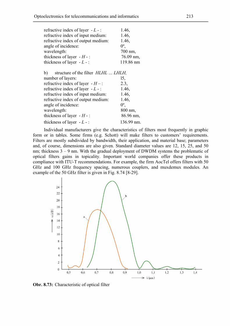
Optoelectronics for telecommunications and informatics 213
refractive index of layer - L - : 1.46, refractive index of input medium: 1.46, refractive index of output medium: 1.46, angle of incidence: 0º, wavelength: 700 nm, thickness of layer - H - : 76.09 nm, thickness of layer - L - : 119.86 nm b) structure of the filter HLHL … LHLH, number of layers: l5, refractive index of layer - H – : 2.3, refractive index of layer - L - : 1.46, refractive index of input medium: 1.46, refractive index of output medium: 1.46, angle of incidence: 0º, wavelength: 800 nm, thickness of layer - H - : 86.96 nm,
thickness of layer - L - : 136.99 nm.
Individual manufacturers give the characteristics of filters most frequently in graphic form or in tables. Some firms (e.g. Schott) will make filters to customers’ requirements. Filters are mostly subdivided by bandwidth, their application, and material base; parameters and, of course, dimensions are also given. Standard diameter values are 12, 15, 25, and 50 nm; thickness 3 – 9 nm. With the gradual deployment of DWDM systems the problematic of optical filters gains in topicality. Important world companies offer these products in compliance with ITU-T recommendations. For example, the firm AocTel offers filters with 50 GHz and 100 GHz frequency spacing, numerous couplers, and muxdemux modules. An example of the 50 GHz filter is given in Fig. 8.74 [8-29].
Obr. 8.73: Characteristic of optical filter
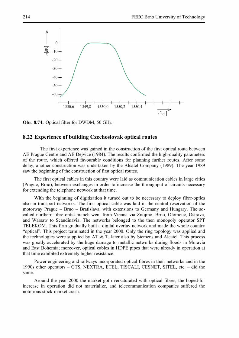
214 FEEC Brno University of Technology
Obr. 8.74: Optical filter for DWDM, 50 GHz
8.22 Experience of building Czechoslovak optical routes
The first experience was gained in the construction of the first optical route between AE Prague Centre and AE Dejvice (1984). The results confirmed the high-quality parameters of the route, which offered favourable conditions for planning further routes. After some delay, another construction was undertaken by the Alcatel Company (1989). The year 1989 saw the beginning of the construction of first optical routes.
The first optical cables in this country were laid as communication cables in large cities (Prague, Brno), between exchanges in order to increase the throughput of circuits necessary for extending the telephone network at that time.
With the beginning of digitization it turned out to be necessary to deploy fibre-optics also in transport networks. The first optical cable was laid in the central reservation of the motorway Prague – Brno – Bratislava, with extensions to Germany and Hungary. The so-called northern fibre-optic branch went from Vienna via Znojmo, Brno, Olomouc, Ostrava, and Warsaw to Scandinavia. The networks belonged to the then monopoly operator SPT TELEKOM. This firm gradually built a digital overlay network and made the whole country “optical”. This project terminated in the year 2000. Only the ring topology was applied and the technologies were supplied by AT & T, later also by Siemens and Alcatel. This process was greatly accelerated by the huge damage to metallic networks during floods in Moravia and East Bohemia; moreover, optical cables in HDPE pipes that were already in operation at that time exhibited extremely higher resistance.
Power engineering and railways incorporated optical fibres in their networks and in the 1990s other operators – GTS, NEXTRA, ETEL, TISCALI, CESNET, SITEL, etc. – did the same.
Around the year 2000 the market got oversaturated with optical fibres, the hoped-for increase in operation did not materialize, and telecommunication companies suffered the notorious stock-market crash.

Optoelectronics for telecommunications and informatics 215
Currently in this country, only sporadic construction of optical routes takes place; routes are being moved (in connection with motorway construction) and wavelength multiplexers are being connected in operationally overloaded fibres.
The construction of FTTH networks currently attracts much attention. In 2007 a pilot network of the type of FTTH was launched in Bohuňovice. The project was realized with EU support funding. In addition to the conventional potentials of this network, automated reading of water consumption is envisaged (and consequently also the supervision of the water-supply pipeline).
Optical cables are in most cases installed by specialized firms, which are properly equipped for this work. Equipment and devices for “fibre-optic” are costly. The basic outfit includes blowing equipment, air compressor, fibre cleaver, splicing machine, optical power source and meter, and reflectometer (OTDR). Tools, cleaning facilities, etc. are indispensable. After installation the final measurements are performed, by the direct method and OTDR (from both ends A and B) and the route is then handed over to the operator.
8.23 Experience of building metropolitan optical network in Brno
After graduating from the Technical University of Brno (TUB) in 1968 the author of the present book was with the firm Czechoslovak Telecommunications, trunk transmission division. After transferring to TUB, he participated, among other things, in building the TUB data network, which was formed by interconnecting individual localities by coaxial (mostly self-supporting) cables and radio links.
After the arrival of “optics” the author (together with Ing. O. Dostal, CSc. – Masaryk University) took part in the first pilot project of optical interconnection of the computer centres of MU and TUB, using an optical cable (ca. 4 km long).
In the first stage, MU and TUB discussed with SPT TELECOM the possibility of the network being built by the latter. After lengthy and unsuccessful negotiations, MU and TUB decided in 1993 to build their own private optical computer network under the name Brno Academic Computer Network (BACN). Because of limited funding and the high cost (in terms of money and time) of buried cables, the network was built using self-supporting optical cable installed on Brno roofs. The terminal devices for the network are also very expensive and therefore, with regard to the price, self-supporting gradient fibre 62.5/125 μm without metallic element was chosen. The cable contained a total of 8 MM optical fibres. Cables for indoor lines have 4 fibres. Outdoor and indoor fibres are fused and housed in cable joints. These cable joints are placed in lockable cabinets to prevent access to them. At each point where a router is mounted, the indoor fibres are brought to a distribution box. The whole network was operated on ETHERNET at 10 Mbit . s-1.
The second stage of building the BACN network was started at the turn of 1996 by the implementation of the “Project of the development of Brno Academic Computer Network” and by upgrading the network. The aim of the project was to extend the network to further localities and enable further institutions to connect to the backbone optical network. The project was funded from the Dynamic Development fund. For the interconnection of localities 8 single-mode fibres (SI) and 4 gradient fibres (GI) were used.
In subsequent years, buried routes were mainly built and this was done either by building new routes to university localities (in view of their importance) or by additionally laying cables in trenches dug out by other firms building private cable networks. Because of the shift in the requirements of the network technologies used the currently laid cables have

216 FEEC Brno University of Technology
only single-mode fibres, mostly 48 or 96 fibres (SI). The firms NETPROSYS and AVENET participated significantly in the development of the network.
When the network began to be built, much emphasis was placed on the maximum possible extension of the network. In the course of time, requirements for increased network quality and bandwidth came to be raised. At that time it was considered convenient to build a new backbone network (ATM), which in addition to high-speed transmissions brings a number of further services. Among them is the possibility of creating virtual networks, which are absolutely necessary in medical applications. Changes were made in the localities Botanická (UVT MU), Obilní trh (Faculty of Medicine, MU) and Kotlářská (Faculty of Science, MU). These changes and the effort to make maximum use of network potentials led to subsequent adjustments in the network distribution system in both the Metropolitan network and some localities. The most dramatic change concerned the Kotlářská locality (the most important locality as regards network operation), where the whole network topology was changed. The changes that were made increased the speed of ETHERNET from 10 Mbit . s-1 to 155 Mbit . s-1.
Exploiting the changes made gave rise to new applications in the field of medicine and initiated the realization of larger systems that provided students and lecturers with access to databases containing, for example, X-ray photographs of patients from various periods of treatment, results of tomographic examinations, angio-examinations, etc. Implementing the Obilní trh node enabled deploying this technology straight at the data source.
A further stage in building the BACN network began only in 2001 because thanks to the preceding highly positive changes made in the backbone network there was no urgent need to rebuild it. At that time a new advanced alternative appeared, namely to build a new backbone network based on the gigabit Ethernet technology. The new gigabit backbone network was built in the year 2002. While building this network, there was a radical change: until the end of last century a network was built by the method of successive steps, i.e. as new requirements for communication appeared and financial resources became available, the network topology was gradually defined. The new gigabit backbone network was built by the big bang method, i.e. the network structure and topology were defined at the very beginning and the building process was then affected by allocation of funds. Today the network contains over 90 important and basic nodes. Currently, the total length of optical fibres and cables amounts to more than 150 km. Through the Masaryk University node the network is connected with Prague via a 2.5 Gbit . s-1 link. From Prague the connection is worldwide.
An ever increasing network with growing numbers of users thus came into being. The network (BACN) currently interconnects universities, Academy-of-Science sites, courts of justice, tax offices, governmental offices, hospitals and other facilities with access to the network. The building of BACN falls into several stages. A new stage of building the BACN network mostly starts when upgrading the power and extent of the network is possible or when new funding is allocated. The users of this network include Vodafone, O2, and other organizations. The schematic diagram of the current network is shown in Fig. 8.75.
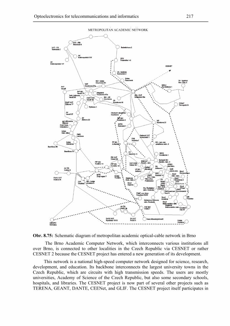
Optoelectronics for telecommunications and informatics 217
Obr. 8.75: Schematic diagram of metropolitan academic optical-cable network in Brno
The Brno Academic Computer Network, which interconnects various institutions all over Brno, is connected to other localities in the Czech Republic via CESNET or rather CESNET 2 because the CESNET project has entered a new generation of its development.
This network is a national high-speed computer network designed for science, research, development, and education. Its backbone interconnects the largest university towns in the Czech Republic, which are circuits with high transmission speeds. The users are mostly universities, Academy of Science of the Czech Republic, but also some secondary schools, hospitals, and libraries. The CESNET project is now part of several other projects such as TERENA, GEANT, DANTE, CEENet, and GLIF. The CESNET project itself participates in

218 FEEC Brno University of Technology
the development of medical applications with other EU countries (e.g. the university in Bologna) in an effort to design pilot projects for the European Union.
Obr. 8.76: Schematic diagram of high-speed computer network for science, research and education – CESNET 2
The CESNET 2 network is connected to the European network GEANT, which is an
association of 30 operators of national academic networks in Europe. In mid 2004 the GEANT project concentrated on further developing the European academic backbone network called GEANT 2.The project is scheduled for 4 years. At present, the speed of GEANT network is up to 10 Gbit . s-1 (see Fig. 8.77).

Optoelectronics for telecommunications and informatics 219
Obr. 8.77: Schematic layout of GEANT embracing national academic networks
Examples of network exploitation
Apart from the standard application of the Internet, the network is utilized for editing journals, E-learning, and voice and video transmission; current interest is focused on the transmission of medical data, pictures, and videoconferencing.
The interdisciplinary project MeDiMed (Metropolitan Digital Imaging System in Medicine) solves problems of medical applicability, legal aspects, and problems of the technical assurance itself.
It is concerned with building a metropolitan archive, so-called PACS (Picture Archiving and Communication System), and with interconnecting hospital modalities (diagnostic facilities) such as ultrasound (US), digital mammography (DMG), computer tomography (CT), magnetic resonance (MR), etc.
The aim is to exploit medical informatics for increasing the quality of medical operativeness and medical care, and for improving the conditions of medical research and teaching of graduates in medicine.
Solving these problems involves archiving image data, transmission of high-quality pictorial information between individual sites (hospitals) with which the patient came into contact during treatment, holding remote consultations with specialists or preparing a plan and simulation of future treatment.

220 FEEC Brno University of Technology
The result is easier and quicker formulation of correct diagnosis, avoidance of repeated examinations, savings in patient’s and doctor’s time and thus also financial means.
This system, which is part of the MeDiMed project, was set up for processing, transmitting and archiving medical information and data in 1999. In that same year the first modalities were connected to the system. One of the primary tasks of the system was the conversion of data into the DICOM (Digital Imaging Communications in Medicine) format. In the year 2000, after the basic trial period, the research workers obtained much specific information concerning the potentials and limitations of the installed PACS system.
DICOM is a format for archiving medical data that has gained worldwide acknowledgement. This format is also used by the MeDiMed project and its PACS central archive for data archiving and transmission. The format must contain all the data necessary for the archived studies to have a trustworthy informative value such as the key words of the study for easy retrieval, description of the study and possibly the procedure adopted in the treatment, and visual documentation.
Information transmitted for the MeDiMed project represents a very sensitive matter since patient’s personal data are involved which no unauthorized person must get hold of. Hospitals make heavy demands on the security of transmitted data. Researchers therefore concentrate on two important facts:
- Securing the BACN network against physical damage or getting hold of important information. For the sake of sufficient security of sensitive data on servers and archiving devices the main servers were placed in a separate, physically partitioned and locked section. The arrangement is similar in the stand-by centre of the Faculty of Medicine of Masaryk University in Brno.
- Getting hold of information about patients via the network. This method of endangering patient’s information is in optical fibre transmission of data protected by a secret method of data ciphering. The archived data are protected by a number of access and protection passwords. The archiving system is divided into several levels, which protect the whole system. Authenticated access provides a further protection of the data and system. The application of firewalls is an important form of protecting data against abuse. Before the input into the transmission network the central PACS servers terminate in a firewall, which ensures the filtering of operation. At the hospital side there is a compiler firewall (administered by the PACS system), which is connected to the hospital boundary router. In this way the security of the PACS system is assured.
A range of diverse hospital workplaces are currently connected to the metropolitan PACS server. Decisive in the identification of individual workplaces is today the IP address of the workstations of the respective workplace. This solution is fully satisfactory only for sources of image data or viewing stations used only by a single user. An alternative to authenticated access is a logical requirement on the part of doctors (on duty in other hospitals, mobile surgeries, doctors working at home, …). This problem was solved by assigning private unique IP addresses to individual users. Another step in this direction consisted in determining the device that would determine one’s private IP address using the PKI (Private Key Infrastructure). The solution chosen was the application of USB keys.
A very important advantage of the project consists in that it is supported by the technology of an instruction and research subsystem, which is expected to greatly enhance the level of teaching undergraduate and postgraduate students of medicine. The solution is conceived such that it fully meets the requirements of compatibility with systems working in

Optoelectronics for telecommunications and informatics 221
real operation; the aim is to create for the user an environment that basically does not differ from real operational systems.
This is closely related to the problem of providing and securing pictorial studies that are suitable for research and instruction purposes as part of the instruction system. All information is removed (or modified) that might reveal patient’s identity but with a maximum informative value of the study being preserved. In 2004 the development of an anonymization module was completed that enabled transmitting selected anonymized studies to the database of the instruction and research system.
A pictorial study that has been included in the instruction system must be provided with a standard description of patient’s problem, with the treatment procedure attached. A set of key words must also be provided to enable simple retrieval of study materials.
Tremendous advances in the development of medicine and diverse technical devices and instruments, together with the great potentials of diagnostics and medical examination, offer new possibilities of exploiting the PACS picture system. Until recently the situation was such that the application of this information remained on the level of doctor’s subjective evaluation. Today, performing a number of examinations (most frequently CT and MR because these methods can provide 3D information on patient’s internal structures) and their mutual evaluation offers the possibility of creating 3D models (modelling of bones and tissues based on the above CT and MR examinations), planning surgical and reconstruction operations, simulations of operation procedures, tool navigation and aiming, and, last but not least, a realistic training of the operation using a simulator. This new possibility began to be developed beyond the initial frame of the MeDiMed project by 3D modelling of tissues on the basis of CT/MR data. Starting from a design of clinically utilizable system of processing CT and MR data for creating 3D computer models of human tissues, the so-called “Virtual development and application centre” was established. Virtual only because it involves highly interdisciplinary cooperation in the fields of state-of-the-art medicine, mechanical engineering, and information technology. To build a unified centre embracing all the necessary fields would be very demanding in terms of funding, personnel and technology. Thus workers engaged in this programme remain in their current position and communicate via the CESNET 2 network. This solution in the form of virtual centre is of great advantage because it saves time (of doctors and technicians) and capacities of very special and costly equipment (CT, MR, 3D printers, software, etc.) necessary for the creation of 3D computer models. Since a future extension of the exploitation of pictorial information is envisaged, the establishment of “only” a virtual centre has the added advantage of easy connection of further localities to the project.
For example, doctors of Thomayer Faculty Hospital (TFH) have shown much interest in this area because they need neurosurgical consultations with the Central Military Hospital (CMH) in Střešovice when treating complicated polytraumata (mostly victims of road accidents) and do not have their own neurosurgical team. They are often challenged to decide whether to continue a treatment within accident surgery or to send the patient to the neurosurgery ward for immediate operation. A strict requirement on the part of CMH specialist is that the consultation for TFH must not tax them too much. Therefore they insist on processing the picture under consultation in their standard environment. In practice this means including the TFH pictures under consultation in the CMH system as if pictures from their specialized centre were concerned.
In addition to increased quality of treatment, the impeccably working MeDiMed system also brings savings in cost and storage room. Information archived today by PACS needed formerly a great amount of paper, rolls of film and other material, the purchase price of which

222 FEEC Brno University of Technology
was not exactly cheap. With the MeDiMed system, which operates without much financial demand, there are savings both in cost and in the storage room that was formerly necessary for such an amount of materials [8-30], [8-31], [8.32].
8.24 Selected examples of optical networks of various operators
As mentioned earlier, the year 2000 witnessed a boom in the construction of optical cable networks. Czech firms competed in laying cables, which eventually led to the current glut of fibre capacities, which are not in operation. Some examples of the construction of networks for various operators will be given below.
The firm Czechoslovak Communications, later Czech Telecom, now Telefónica O2 is one of the big (if not monopolistic) operators, above all thanks to the huge access (subscriber) networks. It was one of the first pioneers in the construction of an optical link, 4 km long, between the Automatic Exchange (AE) in Prague-Centre and the AE in Prague-Dejvice, where the installation of 8-fibre gradient cable (manufactured by the Japanese firm SUMITOMO) was tested.
Subsequently, further junction cables were installed between exchanges all over the Czech Republic with the aim of increasing the channel capacities in large cities.
Around the year 1985 numerous local optical networks were built, as well as optical networks in HV switching stations, in engineering plants, etc.
The first long-distance optical cable using SI fibres connected Prague, Brno, and Bratislava (it is buried in the motorway central reservation), later it was extended to cover Germany and Hungary. Another, northern branch was later built from Vienna via Brno, Olomouc, Ostrava, and Warsaw to Scandinavia.
After the 1990s the Czech Telekom network started to be digitized. Construction by the method of “digital overlay network” (DON) was chosen; the construction was finished towards the end of 2000. The optical circuits built assure failure-free operation. The O2 network is shown schematically in Fig. 8.78. Basically, the network has been completed, and currently wave multiplexers are being deployed along the backbone route. The network is based on optical cables made by the firms OFS (Lucent Technologies AT&T) and Samsung. It has some 30000 km of optical cables, which roughly corresponds to 800 000 km of fibres. The cables have 24, 48 or 96 fibres. From the competitors’ viewpoint, O2 has most fibres and uniform coverage with termination in the centres of cities.
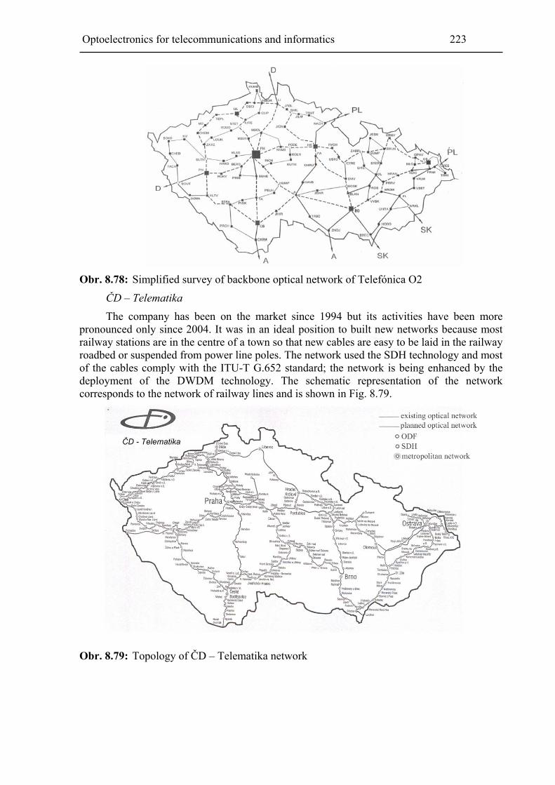
Optoelectronics for telecommunications and informatics 223
Obr. 8.78: Simplified survey of backbone optical network of Telefónica O2
ČD – Telematika
The company has been on the market since 1994 but its activities have been more pronounced only since 2004. It was in an ideal position to built new networks because most railway stations are in the centre of a town so that new cables are easy to be laid in the railway roadbed or suspended from power line poles. The network used the SDH technology and most of the cables comply with the ITU-T G.652 standard; the network is being enhanced by the deployment of the DWDM technology. The schematic representation of the network corresponds to the network of railway lines and is shown in Fig. 8.79.
Obr. 8.79: Topology of ČD – Telematika network

224 FEEC Brno University of Technology
Obr. 8.80: Topology of ČEZ ICT Services
The services offered include: voice services, Internet connection, IP protocol services,
hire-out of fibres (SM 9/125 μm), hire-out of circuits (from 2 Mbit . s-1 to 2.5 Gbit . s-1). Security supervision and monitoring of the network [8-33].
ČEZ ICT Services network
The company ČEZ ICT Services, a.s., ranks with advanced providers of fully convergent ICT services. Through its own huge infrastructure it provides attractive ICT services in interesting groupings and with a varied range of applications. The special position of the company is based on the contractual association with its owner, the parent company ČEZ, a.s.
Many years’ experience in the area of providing services for power engineering is a tested means to complex and highly professional services of guaranteed high quality.
In connection with the expansionist policy of the parent company ČEZ, the ČEZ ICT Services Company participates in consultation and integration solutions both at home and abroad, from proposing the design through to its practical implementation.
The company is a member of the international association of power engineering operators 4cE (For Connecting Europe), a member of RIPE (Reseaux IP Europeens), APVTS (Association of operators of public telecommunications networks), and NIX.CZ (Neutral Internet eXchange).
The total length of the company’s backbone optical network exceeds 7 000 km. The nodes, which are mainly located in power engineering facilities (power plants, switching stations, etc.) and in regional and former district capitals as well as in other locations all over the Czech Republic, are equipped with transmission technologies allowing digital transmission in 64 kbit . s-1 to 2.5 Gbit . s-1 capacities. The backbone network utilizes the wavelength division multiplex (DWDM), synchronous digital hierarchy (SDH), and
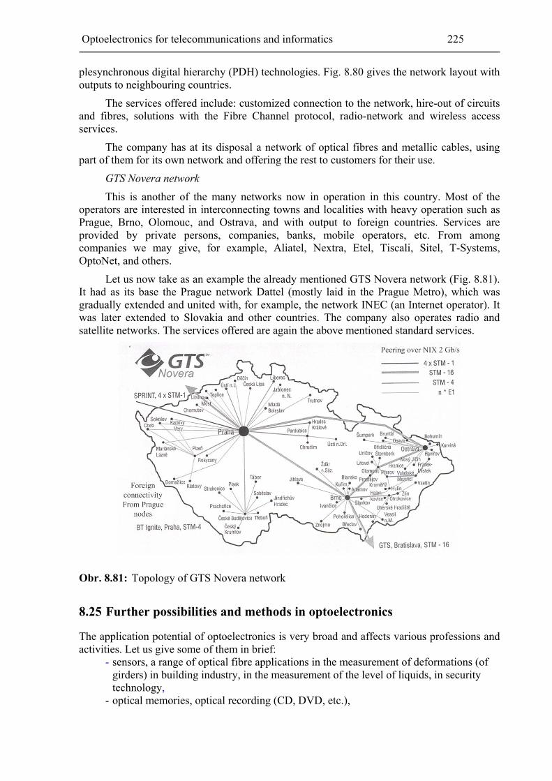
Optoelectronics for telecommunications and informatics 225
plesynchronous digital hierarchy (PDH) technologies. Fig. 8.80 gives the network layout with outputs to neighbouring countries.
The services offered include: customized connection to the network, hire-out of circuits and fibres, solutions with the Fibre Channel protocol, radio-network and wireless access services.
The company has at its disposal a network of optical fibres and metallic cables, using part of them for its own network and offering the rest to customers for their use.
GTS Novera network
This is another of the many networks now in operation in this country. Most of the operators are interested in interconnecting towns and localities with heavy operation such as Prague, Brno, Olomouc, and Ostrava, and with output to foreign countries. Services are provided by private persons, companies, banks, mobile operators, etc. From among companies we may give, for example, Aliatel, Nextra, Etel, Tiscali, Sitel, T-Systems, OptoNet, and others.
Let us now take as an example the already mentioned GTS Novera network (Fig. 8.81). It had as its base the Prague network Dattel (mostly laid in the Prague Metro), which was gradually extended and united with, for example, the network INEC (an Internet operator). It was later extended to Slovakia and other countries. The company also operates radio and satellite networks. The services offered are again the above mentioned standard services.
Obr. 8.81: Topology of GTS Novera network
8.25 Further possibilities and methods in optoelectronics
The application potential of optoelectronics is very broad and affects various professions and activities. Let us give some of them in brief:
- sensors, a range of optical fibre applications in the measurement of deformations (of girders) in building industry, in the measurement of the level of liquids, in security technology,
- optical memories, optical recording (CD, DVD, etc.),

226 FEEC Brno University of Technology
- laser printers, - holography (3D recording), - medicine (diagnostics, ophthalmology, surgery), - spectral analysis, - displays, - broad application in industries, - measurement technology.
A more detailed description would be beyond the scope of the present publication.
To conclude this sub-chapter, let us stress in brief two areas that are connected with our thematics.
Security technology - this concerns the problematic of using optical fibres (cables) in the protection of objects (airports and similar). These systems are based on microbends in fibres caused by the fibres being trod on or by touching a fence in which the fibres are built in. They are referred to as perimetric security systems. Changes in the fibre are detected and evaluated and subsequently alarm may be raised. These are very reliable systems. For details the reader is referred to the technical manual of the firm Security technologies [8-34].
From the viewpoint of the optoelectronic systems described above it is necessary to draw up a design of the system, calculate the technical parameters and propose the project. Using a software solution can in many cases make this work easier. In network design it is possible to use, for example, the OPTISIM program [8-35] or the MATLAB & Simulink program kit (HUMUSOFT [8-36]). Leading design firms include INTAR, SUDOP, etc.
8.26 Health protection during work with optical links
When laying and installing optical cables it is necessary to observe the respective safety-at-work regulations, in particular those concerning work in cable cellars, work with inflammable materials, and work in public communications spaces.
When working with optical cables, workers will get in touch with organic solvents, substances that form the filler material, and the glass material of the optical fibres themselves. In all these situations, increased standards of personal hygiene must be observed. Special attention must be paid to optical glass fibres, which must be cleaved, cleaned and otherwise handled during installation. Glass splinters are particularly dangerous since they can cause injuries to the skin and eyes. It is therefore imperative to handle the fibre with utmost care and gather all glass splinters in a special case (box) with some oil in it.
During the work with optical cables, human health can be at risk also due to light radiation, which in telecommunications systems is between 780 and 1650 nm (visible light region 400 – 700 nm). With these wavelengths living tissues can at excessive intensity be damaged. Considering the powers of sources of optical radiation, which range form several mW up to 1 or 2 W during pulsed mode, the human eye is at risk of burnt retina, inflammation or cataract of the lens of the eye.
Even higher powers occur in free-space communication, where the LD transmission elements are combined into high-power radiators.
In the course of building, maintaining and repairing optical telecommunication cables light sources are being disconnected from the optical fibre, fibre ends containing radiation are being handled, optical connectors are being disconnected, etc. It is therefore necessary to respect the following principles:
Optoelectronics for telecommunications and informatics 227
- The distance from which the active area of an optical element (fibre, connector, etc.) is being observed from which radiation is emitted must not be less than 25 cm.
- Places from which optical radiation is emitted can be viewed through optical devices (magnifying glass, microscope) only with the radiation source turned off.
9 Measuring methods in optical communications
The development of optoelectronic telecommunication systems has entailed the development of new measuring methods and instruments for the measurement of the parameters of fibres, cables and other optoelectronic elements. At first glance it might seem that the measuring methods are analogous to the methods used for metallic lines but in fact they are markedly different. Take, for example, the measurement of attenuation: the name is the same in both cases, the theoretical foundation is the same but the approach is completely different. The difference in measuring methods is given by the specific properties and behaviour of light.
Leading manufacturers of optoelectronics currently offer a whole range of measuring devices that feature simple operation and rapid measurement. The instruments are in most cases provided with standardized connectors for optical radiation input and output.
For the area of optical measurement numerous recommendations have been worked out in IEC, ITU-T and DIN, others are in the stage of preparation and much has still to be done, in metrology in particular.
Optical measuring methods can be divided from various points of view; in the following we will stick to this division:
Measurement on optical fibres; - optical measurement - mechanical measurement. Transmission measurement on optical fibres: - measurement of attenuation, - measurement of dispersion, - measurement of polarization mode dispersion, - measurement of backscatter; - measurement of bandwidth. Measurement of optoelectronic components. Special measuring methods.
Measuring instruments.
Another division can be from the viewpoint of application: for example, measuring methods for the manufacture of optical fibres, measuring methods for the manufacture of optical cables, measuring methods for the installation of cables, and measuring methods for operational measurement.
From the viewpoint of building an optical track the following measurement must be taken into account:
- preparatory measurement (prior to acceptance inspection and prior to installation), - measurement during cable installation, - measurement on an installed route, - final measurement (acceptance inspection after installation), - measurement during device installation,

228 FEEC Brno University of Technology
- regular check measurement of operation, - localization of possible failures on optical track, - check measurement of time stability of devices, - permanent check of the working of the whole optical system, - experimental measurement.
Most of the measurement consists in establishing the parameters of optical fibre and the properties of optoelectronic modules of the system. The measurement set includes a permanent check of the working of the system, which consists in electrical measurement of error rate and its evaluation.
9.1 Methods of optical fibre excitation for measuring purposes
Since the lightguide is never ideally straight and cylindrical but exhibits random bends and cross-section ellipticity, rays propagating in it are also liable to random changes. New modes can be formed on fibre inhomogeneities that were not present in the mode distribution before this inhomogeneity and, on the contrary, modes can disappear (by emission into the jacket or by absorption) that till then participated in the transmission. This event is known as mode overflow, the so-called mode conversion.
After a certain passage through optical fibre (of several units to hundreds of metres) there is a certain balance in the distribution of power into individual modes, so-called stable mode distribution. This state is highly desirable for the conditions of correct measurement of optical fibre parameters.
When this requirement is not respected the measurement can, due to the existence of differential attenuation, carry an error that completely distorts the results. When measuring close to the source in particular, the mode distribution changes and does not guarantee measurement reproducibility.
Conditions of stable mode distribution also for verification on short sections can be approximated by using special devices inserted between the source and the fibre being measured. It is possible to use:
- couplers, - mode scramblers, - mode filters.
Couplers are used for specific coupling of optical power to the fibre being measured, i.e. with exactly determined numerical aperture and with the required size of beam trace. The couplers can be of the classical type, i.e. made up of lenses and diaphragms or of the fibre type, with a fibre of suitable parameters.
In the mode scrambler heavy decoupling (mixing) of modes takes place, which leads to a homogeneous distribution of power on its output [9-41].
The mode filter is used to remove undesirable higher modes before the input to the unit being measured.
Coupler realizations for a fibre of 50 μm in diameter and theoretical numerical aperture NA = 0.2, inclusive of the coupling condition, are standardized in IEC. According to this recommendation, the mode distribution can be considered stable when after the passage of radiation through a fibre 2 m long the beam half-width measured in the near region is 26 ± 2 μm and the numerical half-aperture measured in the far region is NA = 0.11 ± 0.02.
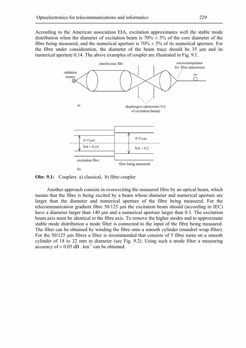
Optoelectronics for telecommunications and informatics 229
According to the American association EIA, excitation approximates well the stable mode distribution when the diameter of excitation beam is 70% ± 5% of the core diameter of the fibre being measured, and the numerical aperture is 70% ± 5% of its numerical aperture. For the fibre under consideration, the diameter of the beam trace should be 35 μm and its numerical aperture 0.14. The above examples of coupler are illustrated in Fig. 9.1.
Obr. 9.1: Couplers a) classical, b) fibre coupler
Another approach consists in overexciting the measured fibre by an optical beam, which
means that the fibre is being excited by a beam whose diameter and numerical aperture are larger than the diameter and numerical aperture of the fibre being measured. For the telecommunication gradient fibre 50/125 μm the excitation beam should (according to IEC) have a diameter larger than 140 μm and a numerical aperture larger than 0.3. The excitation beam axis must be identical to the fibre axis. To remove the higher modes and to approximate stable mode distribution a mode filter is connected to the input of the fibre being measured. The filter can be obtained by winding the fibre onto a smooth cylinder (mandrel wrap filter). For the 50/125 μm fibres a filter is recommended that consists of 5 fibre turns on a smooth cylinder of 18 to 22 mm in diameter (see Fig. 9.2). Using such a mode filter a measuring accuracy of ± 0.05 dB . km-1 can be obtained.

230 FEEC Brno University of Technology
Obr. 9.2: Mode filter
Perfect stable mode distribution can be obtained in such a way that a 1000 m section of so-called dummy fibre (pre-fibre) is inserted between the transmitter and the fibre being measured, as shown in Fig. 9.3.
Obr. 9.3: Efficiency of mode filtering
The filter quality can be assessed using the filter efficiency criterion ΔΘ according to the relation
%,1002
12
Θ
ΘΘΘ
(9.1)
where Θ1 is the angle of a beam exiting a fibre element 1 km long, Θ2 is the angle of a beam exiting a fibre 2 m long, coupled to a mode filter (see Fig. 9.3).
Mode scramblers can also act as mode filters: because of the coupling of higher modes in mode scramblers, they act as filters. Examples of a mechanical scrambler and a serpentine scrambler (the fibre is intertwined with seven cylinders of 1 cm in diameter, their centres are spaced 1.3 cm) are given in Fig. 9.4. Mode scramblers made from different types of fibre are shown in Fig. 9.5. The first of them, made up of different bits of fibre, is frequently used in
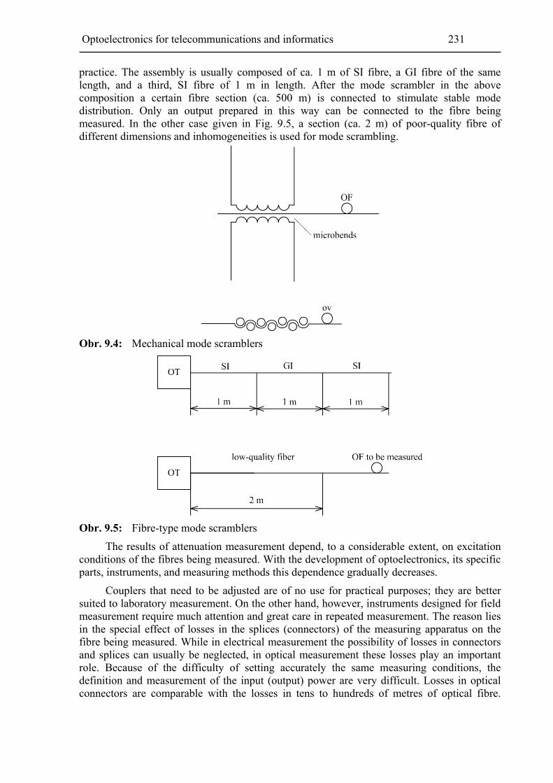
Optoelectronics for telecommunications and informatics 231
practice. The assembly is usually composed of ca. 1 m of SI fibre, a GI fibre of the same length, and a third, SI fibre of 1 m in length. After the mode scrambler in the above composition a certain fibre section (ca. 500 m) is connected to stimulate stable mode distribution. Only an output prepared in this way can be connected to the fibre being measured. In the other case given in Fig. 9.5, a section (ca. 2 m) of poor-quality fibre of different dimensions and inhomogeneities is used for mode scrambling.
Obr. 9.4: Mechanical mode scramblers
Obr. 9.5: Fibre-type mode scramblers
The results of attenuation measurement depend, to a considerable extent, on excitation conditions of the fibres being measured. With the development of optoelectronics, its specific parts, instruments, and measuring methods this dependence gradually decreases.
Couplers that need to be adjusted are of no use for practical purposes; they are better suited to laboratory measurement. On the other hand, however, instruments designed for field measurement require much attention and great care in repeated measurement. The reason lies in the special effect of losses in the splices (connectors) of the measuring apparatus on the fibre being measured. While in electrical measurement the possibility of losses in connectors and splices can usually be neglected, in optical measurement these losses play an important role. Because of the difficulty of setting accurately the same measuring conditions, the definition and measurement of the input (output) power are very difficult. Losses in optical connectors are comparable with the losses in tens to hundreds of metres of optical fibre.

232 FEEC Brno University of Technology
Moreover, even in types of the highest quality there are certain fluctuations in losses in repeated installation, which are difficult to define generally.
In the first place, they are losses due to connector design tolerances, in particular axial misalignment, imperfect contact of fibre edges, and faulty fibre cleavage. In practice this means the impossibility to measure with a greater accuracy than these uncertain losses in connectors. Since connectors are deployed on the transmitting as well as the receiving side, we are faced here with a fundamental limitation of the potential measuring accuracy (above all the measurement of optical powers). For these reasons the measurement of optical fibres is conducted at both ends and the average value is then established [9-2].
Formation of optical flux
Laser diodes (LD) or light-emitting diodes (LED) are used as stabilized sources. The output level of LD depends on temperature and reflected light. To remove changes caused by this dependence the output level is monitored and, using the feedback loop, the output level is stabilized.
A stabilized source operating on the 1.3 μm wavelength requires the surrounding temperature to be strictly stabilized. This stabilization is provided using a feedback circuit and the Peltier cooling element, see Fig. 9.6.
Obr. 9.6: Stabilized optical source circuit
The temperature characteristic of the output level of stabilized optical source with LD has in the temperature range 5 - 50 ºC a deviation of less than 0.05 dB.
At a constant temperature, LEDs have a stable output level for a long time and with extremely high reliability. But output level is very sensitive to effects of surrounding temperature. If a surrounding temperature sensor with a diode for temperature compensation is used, adequate stability can be obtained. The temperature characteristic of the output level of stabilized optical source with LED has in the temperature range 5 – 50 ºC a deviation of less than 0.5 dB for the 0.85 μm and 1.3 μm bands.
The wavelength of the spectral width of light emitted by stabilized source must also be stabilized. For the sake of measurement accuracy the emitted average wavelength must be around 5 nm.
Some instruments are equipped with temperature control, which eliminates changes in wavelength oscillation caused by changes in surrounding temperature. The light-emitting elements used are LED. Due to their high temperature stability they are also suitable for the measurement of transmission bandwidth.
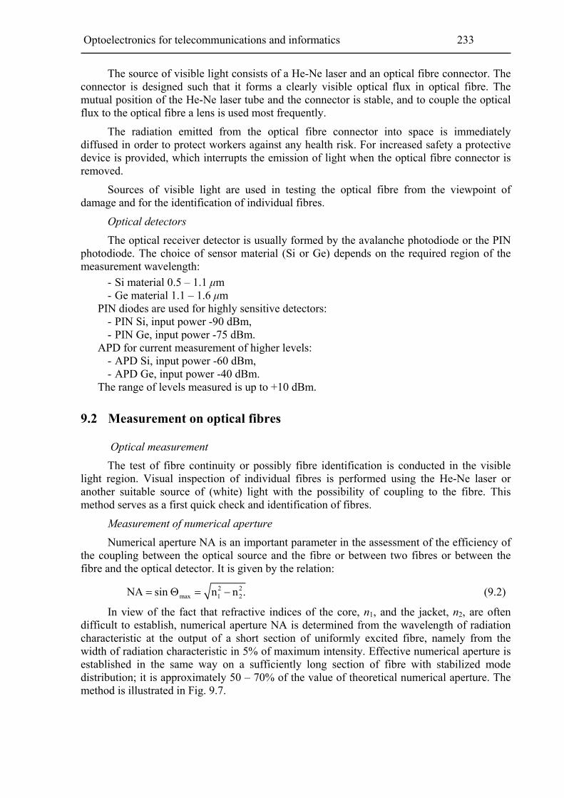
Optoelectronics for telecommunications and informatics 233
The source of visible light consists of a He-Ne laser and an optical fibre connector. The connector is designed such that it forms a clearly visible optical flux in optical fibre. The mutual position of the He-Ne laser tube and the connector is stable, and to couple the optical flux to the optical fibre a lens is used most frequently.
The radiation emitted from the optical fibre connector into space is immediately diffused in order to protect workers against any health risk. For increased safety a protective device is provided, which interrupts the emission of light when the optical fibre connector is removed.
Sources of visible light are used in testing the optical fibre from the viewpoint of damage and for the identification of individual fibres.
Optical detectors
The optical receiver detector is usually formed by the avalanche photodiode or the PIN photodiode. The choice of sensor material (Si or Ge) depends on the required region of the measurement wavelength:
- Si material 0.5 – 1.1 μm - Ge material 1.1 – 1.6 μm
PIN diodes are used for highly sensitive detectors: - PIN Si, input power -90 dBm, - PIN Ge, input power -75 dBm.
APD for current measurement of higher levels: - APD Si, input power -60 dBm, - APD Ge, input power -40 dBm.
The range of levels measured is up to +10 dBm.
9.2 Measurement on optical fibres
Optical measurement
The test of fibre continuity or possibly fibre identification is conducted in the visible light region. Visual inspection of individual fibres is performed using the He-Ne laser or another suitable source of (white) light with the possibility of coupling to the fibre. This method serves as a first quick check and identification of fibres.
Measurement of numerical aperture
Numerical aperture NA is an important parameter in the assessment of the efficiency of the coupling between the optical source and the fibre or between two fibres or between the fibre and the optical detector. It is given by the relation:
2 2max 1 2NA sin n n . (9.2)
In view of the fact that refractive indices of the core, n1, and the jacket, n2, are often difficult to establish, numerical aperture NA is determined from the wavelength of radiation characteristic at the output of a short section of uniformly excited fibre, namely from the width of radiation characteristic in 5% of maximum intensity. Effective numerical aperture is established in the same way on a sufficiently long section of fibre with stabilized mode distribution; it is approximately 50 – 70% of the value of theoretical numerical aperture. The method is illustrated in Fig. 9.7.

234 FEEC Brno University of Technology
Obr. 9.7: Measurement of numerical aperture
The fibre is coupled to the optical transmitter via a suitable coupler. At the fibre output, the optical receiver (detector) is mounted on a swing arm; it detects radiant intensity in dependence on the size of angle Θ measured from the fibre axis.
The dependence of the level of emitted optical power Popt on angle Θ from the end of GI fibre of 2 m in length is given in Fig. 9.8.
Obr. 9.8: Radiation characteristic of GI fibre of 2 m in length
Interference method for measuring refractive index profile. We distinguish two methods, destructive and non-destructive. In the destructive method, a thin slice is separated from the optical fibre and, irradiated by laser, it is examined under interference microscope. The precise value of refractive index is calculated from interference lines. In the non-destructive method the fibre, irradiated by laser and immersed in inert liquid, is examined also under interference microscope.
Measurement of refractive index profile by the near-field method. A lens is placed at the fibre output and a photodiode on the swing arm performs the detection; the recording can be displayed on a screen. In this way the waveform of surface density of radiant intensity is obtained, see Fig. 9.9.
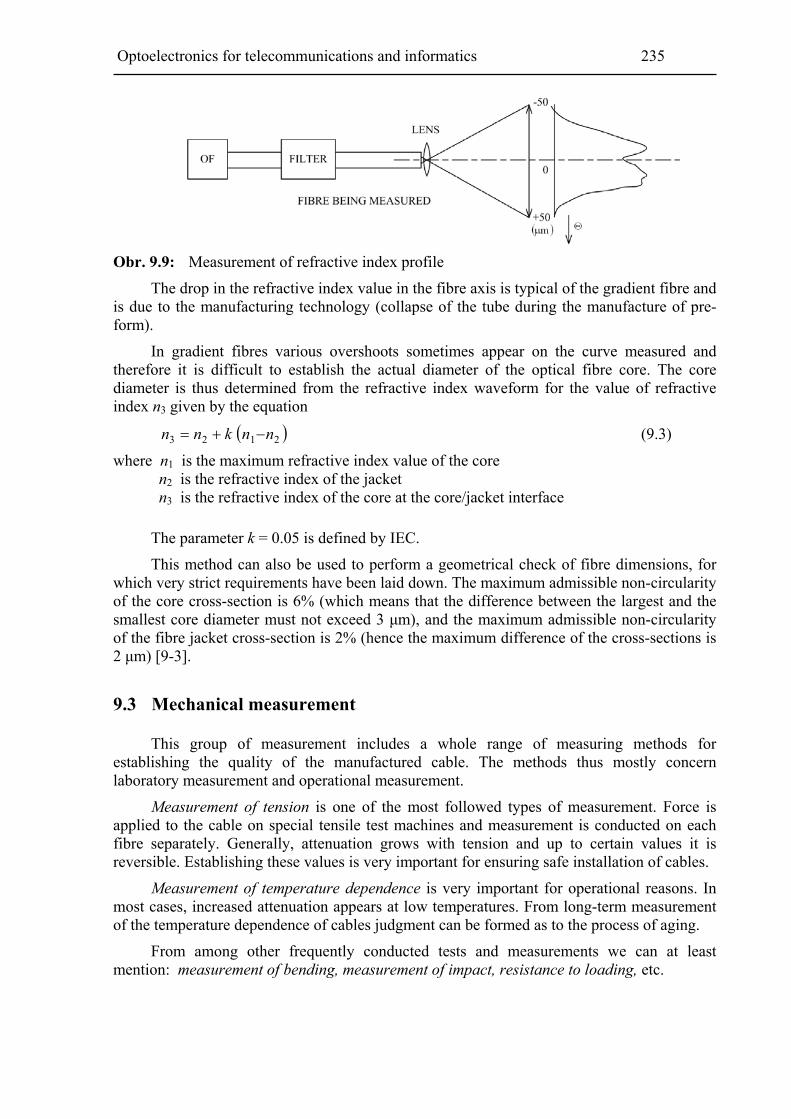
Optoelectronics for telecommunications and informatics 235
Obr. 9.9: Measurement of refractive index profile
The drop in the refractive index value in the fibre axis is typical of the gradient fibre and is due to the manufacturing technology (collapse of the tube during the manufacture of pre-form).
In gradient fibres various overshoots sometimes appear on the curve measured and therefore it is difficult to establish the actual diameter of the optical fibre core. The core diameter is thus determined from the refractive index waveform for the value of refractive index n3 given by the equation
2123 nnknn (9.3)
where n1 is the maximum refractive index value of the core n2 is the refractive index of the jacket n3 is the refractive index of the core at the core/jacket interface
The parameter k = 0.05 is defined by IEC.
This method can also be used to perform a geometrical check of fibre dimensions, for which very strict requirements have been laid down. The maximum admissible non-circularity of the core cross-section is 6% (which means that the difference between the largest and the smallest core diameter must not exceed 3 μm), and the maximum admissible non-circularity of the fibre jacket cross-section is 2% (hence the maximum difference of the cross-sections is 2 μm) [9-3].
9.3 Mechanical measurement
This group of measurement includes a whole range of measuring methods for establishing the quality of the manufactured cable. The methods thus mostly concern laboratory measurement and operational measurement.
Measurement of tension is one of the most followed types of measurement. Force is applied to the cable on special tensile test machines and measurement is conducted on each fibre separately. Generally, attenuation grows with tension and up to certain values it is reversible. Establishing these values is very important for ensuring safe installation of cables.
Measurement of temperature dependence is very important for operational reasons. In most cases, increased attenuation appears at low temperatures. From long-term measurement of the temperature dependence of cables judgment can be formed as to the process of aging.
From among other frequently conducted tests and measurements we can at least mention: measurement of bending, measurement of impact, resistance to loading, etc.

236 FEEC Brno University of Technology
9.4 Transmission measurement on optical fibres
Most of this measurement came to be used to establish the quality of optoelectronic transmission systems.
Measurement of optical power
The measurement of optical power is one of the basic types in the area of optical measurement. This measurement is performed via converting the power of optical beam, which is emitted directly by different optical sources or emanates from optical fibre, to electric signal by means of an optoelectronic (O/E) converter.
An optical power meter consists of three parts: indicator, sensor, and adaptor, see Fig. 9.10. The adaptor adapts the light flux from a source or fibre such that it is best adapted to the sensor dimension, and thus maximum optical power can be delivered to the sensor. The sensor converts optical power to electric power. The indicator serves to display the electric signal on a screen.
Obr. 9.10: Measurement of optical power
These parts of the optical power meter can be exchangeable so that the device can be used for measuring the required wavelength range of the power being measured, and for various types of signal reception.
The measurement enables establishing
- operation of opto/electronic converters and modules (or transmitter and receiver), - losses in fibres (fibre attenuation), - losses in the splices of parts of optical route, - function of passive optical elements (attenuation networks, connectors, optical
switching arrays).
The measurement is conducted on the respective wavelength, which can be set in advance. The choice depends on the electro/optical and opto/electronic converters used, which are fundamental elements of sources and receivers.
The block diagram of an optical power meter is given in Fig. 9.11. To increase the receiver sensitivity, an optical signal chopper with subsequent synchronous detection is used in addition to the generally known blocks (CU stand for control unit). The sensitivity is thus increased by ca. 20 dB.

Optoelectronics for telecommunications and informatics 237
Obr. 9.11: Block diagram of optical power meter
Measurement of attenuation
Attenuation represents the basic and most important transmission parameter and is an overall measure of optical power losses in the optical signal propagation through the fibre. Using the well-known definition, the attenuation of optical fibre between two points (1, 2 – input, output) is determined from the relation
1
2
10 log dB ,P
AP
(9.4)
where P1, P2 are the optical powers (W) for wavelength λ. In the case of stable mode distribution in the fibre, specific fibre attenuation can be
defined for wavelength λ
-1dB.km ,A
(9.5)
where (km) is the distance between point 1 and point 2.
The measurement of attenuation is mostly performed only for discrete wavelengths of 850 nm, 1300 nm, 1310 nm or 1550 nm. The spectral characteristic of attenuation is mainly important to fibre manufacturers.
IEC recommends three methods for the measurement of fibre attenuation:
- cut-back method, - insertion loss method, - backscattering method. Because of its high sensitivity, the cut-back method is recommended as a reference
method (although it is a destructive method). After coupling the optical power from a stabilized optical source (with connected internal or external transmit unit T.J. – coupler, filter) to the measured fibre (Fig. 9.12) of length l, the power is measured at point 2 at the end of the fibre (power meter). With the coupling conditions unchanged, the fibre is cleaved ca. 2 m from the beginning (at point l) and output P1 is measured. Attenuation and specific attenuation of the fibre are calculated using relations (9.4) and (9.6). An accuracy of 0.01 dB . km-1 can be achieved by this method.

238 FEEC Brno University of Technology
Obr. 9.12: Measurement of attenuation by cut-back method
The insertion loss method also requires measuring in two steps. This is an operational
method and is particularly suitable in the case of connectored fibres and cables. In the first place, the measuring equipment must be calibrated via interconnecting the source and the detector (see Fig. 9.13). After measuring we obtain the value of power P1. The fibre being measured is then connected between the optical transmitter and the power meter, and the value of power P2 is obtained. Attenuation and specific attenuation of the fibre are again determined using relations (9.4) and (9.5). In this case, the attenuation measured consists of fibre attenuation and attenuation of the splice of the fibre being measured. In the measurement of connectored cables, the measurement precision is a function of the connector used and is usually worse than 0.2 dB.
Obr. 9.13: Measurement of attenuation by insertion loss method

Optoelectronics for telecommunications and informatics 239
Obr. 9.14: Operational measurement of attenuation, using insertion loss method
The method is used in practice also in such a way that on each side of the route (A, B) both the source (transmitter) and the power meter (receiver) are located. The method proceeds in four steps: two measurements are first made on each side via connecting the power meters to sources (calibration), and two measurements with the fibre connected in both directions. A simplified fundamental schematic is given in Fig. 9.14. The four values of optical power obtained, P11, P12, P21, P22, are used to calculate the operational attenuation of fibre according to the relation
2211
2112
PP
PPA (9.6)
The specific attenuation can be calculated by substituting into (9.7) and (9.6).
If in the above method we want to establish losses in the splices, we use for calibration fibres of 2 to 3 m in length and of the same kind as the fibre being measured. On the assumption that the coupling losses of connecting the reference cable and the cable being measured are the same and the attenuation of reference cable can be neglected, then the attenuation obtained in this way corresponds to losses in the cable alone.
The backscattering method (the principle is described below) for the measurement of fibre attenuation is based on a completely different principle. In the two preceding methods optical power was measured after passage through the fibre while in this method the time dependence of backscattered optical power P (or the level) during pulse propagation in the fibre is evaluated, which yields information on the quality of the whole fibre in dependence on its length (see Fig. 9.15). From this dependence we can establish the attenuation of a homogeneous section of fibre according to the relation
dBlog52
1
P
PA (9.7)
Obr. 9.15: Measurement of attenuation in a splice (fibre values are known)

240 FEEC Brno University of Technology
and the specific attenuation by substituting relation (9.8) into relation (9.6). The meter, an optical reflectometer, is much more complicated than the power meter and, consequently, also more expensive. However, using a display and recorder, the method provides information not only about fibre attenuation but also about the fibre quality (failures, defects) along the whole of its length.
The measurement of attenuation in a splice belongs to important measurements in the construction of optical routes. Immediately after fusing (or otherwise joining) sections of optical fibre it is absolutely necessary to measure and check the quality of the splice made. If the splice is found to be of poor quality, the splice must be made again.
The measurement of attenuation in a splice is laborious and time-consuming, and requires much care. There are two ways how to proceed in practice:
- using the manufacturer’s parameters of the fibres being joined, - without knowing the attenuation of the fibres being joined.
In the first case, the sections of the two fibres to be joined by splice S are from the viewpoint of attenuation known from the measurement protocols provided by the manufacturer. Prior to making the splice S, the level P1 is measured on the side of the first fibre section (see Fig. 9.15). Subsequent to making the splice S, the level P2 is measured on the output of the section being joined. The splice attenuation is determined from the relation
dB221S aPPA , (9.8)
where a2 dB is the attenuation from factory protocols for a specific length and transmission wavelength.
In the second case, when the attenuation of the sections being joined is not known, the procedure is as follows. Prior to fusing, the level P1 is measured on the output of the first section. A provisional splice PS is made (see Fig. 9.16) and the level is measured on the output of the spliced section P2. After the provisional splice, in the direction from the input, the fibre is interrupted and the level P3 is measured. The definite splice DS is made and the value of power level P4 is found. Attenuation V2 of the section being joined is then
2 3 2 dB .A P P (9.9)
Attenuation in the definite splice is
DS 1 4 2 dB .A P P A (9.10)

Optoelectronics for telecommunications and informatics 241
Obr. 9.16: Measurement of attenuation in a splice (fibre values are not known)
In the measurement of connector attenuation a special reference fibre of 2 – 3 m in length is used. It is connected between the transmitter and the receiver, and the level of optical power P1 is measured. The reference fibre is replaced with a fibre obtained by joining two short sections by a connector (the fibre must be of the same length and type as the reference fibre). The level P2 is measured and the connector attenuation is established from the relation
K 1 2 dB .A P P (9.11)
Measurement of backscatter
The backscattering method is an effective means of diagnosing optical fibres. The method provides a detailed picture of the attenuation and possible fluctuations in geometrical and physical parameters along the fibre, inclusive of failure localization.
The method is based on evaluating the time dependence of backscattered power of a narrow optical pulse coupled to the fibre. Backscattered light detected at its input comes from the Fresnel reflections from refractive index discontinuity and from Rayleigh’s scattering on microscopic fluctuations of glass refractive index. The amount of backscattered light is directly proportional to the passing optical power. Changing the intensity of backscattered light enables measuring the fibre attenuation.
The fibre length can be established from the time delay of the reflection from the rear end of fiber with respect to the reflection from the input end.
An analysis of backscattered light provides a picture of the fibre homogeneity (inhomogeneity), and allows monitoring whether the mode distribution has become stable.
Great advantages of the method are its non-destructive nature and the possibility of measuring from one fibre end.
To get a mathematical representation of backscatter signal it is necessary to perform an analysis of light energy on an element of optical fibre, then to consider light scattering on a
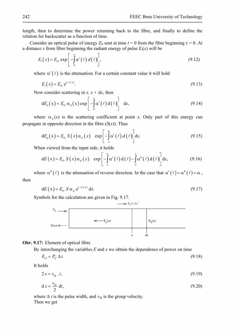
242 FEEC Brno University of Technology
length, then to determine the power returning back to the fibre, and finally to define the relation for backscatter as a function of time.
Consider an optical pulse of energy E0 sent at time t = 0 from the fibre beginning x = 0. At a distance x from fibre beginning the radiant energy of pulse Ei(x) will be
i O
0
exp ,w
E x E d
(9.12)
where is the attenuation. For a certain constant value it will hold
i O e .xE x E (9.13)
Now consider scattering in x, x + dx, then
w
d O d
0
d x x exp d d ,E E x
(9.14)
where d (x) is the scattering coefficient at point x. Only part of this energy can
propagate in opposite direction in the fibre (S(x)). Thus
w
p O d
o
d x exp dE E S x x d x.
(9.15)
When viewed from the input side, it holds
w x
O d
o o
d x exp d d d ,E E S x x x
(9.16)
where is the attenuation of reverse direction. In the case that ,
then
2 α xO dd x e dE E S x. (9.17)
Symbols for the calculation are given in Fig. 9.17.
Obr. 9.17: Element of optical fibre
By interchanging the variables E and x we obtain the dependence of power on time
O OE P t. (9.18)
It holds
sk2 . ,x v t (9.19)
skd d ,2
vx t (9.20)
where Δ t is the pulse width, and vsk is the group velocity. Then we get

Optoelectronics for telecommunications and informatics 243
.eS5,0t tvskdO
vtPP (9.21)
It is clear from the result that backscatter power is dependent on input power Po, pulse width Δt and on the fibre parameters S and αd (αd are losses due to Raileigh’s scattering per unit of length).
The coefficient of backscattering S for a fibre with step refractive index is calculated according to the relation
2
21
3,
8S
n
(9.22)
for a fibre with parabolic refractive index
2
21
,4
Sn
(9.23)
where
2 21 2 .n n (9.24)
The resultant exponential curvature depends on the size of attenuation and on group velocity.
When choosing the pulse width it is necessary to accept a compromise between the requirement for photodiode sensitivity and the resolution power. With increasing pulse length the maximum measurable total attenuation increases but the accuracy of length measurement decreases. The power of reflected radiation is ca. 50 to 60 dB lower than a passing optical pulse and this makes heavy demands on the device sensitivity.
For reasons given above, the design of optical reflectometer is continuously being perfected. Principles known from information theory (problems of signal and noise reception) are applied such as correlation methods and frequency synthesis methods. Also, memories are employed, in which certain values of attenuation of reflected pulses are stored and their average values are evaluated (this reduces measurement errors caused by receiver noise). A more detailed discussion of these methods would be beyond the scope of this publication; this is rather a matter for specialists in the area of measurement in telecommunications.
The fundamental principle and method of backscatter measurement are obvious from the block diagram shown in Fig. 9.18. For the measurement itself it is sufficient to connect the fibre being measured to the input connector of the reflectometer.

244 FEEC Brno University of Technology
Obr. 9.18: Block diagram of pulse reflectometer
The reflectometer is composed of a source of optical pulses, an optical system for splitting the optical beam, and an optical receiver with evaluation of the time interval between the sent pulse and the reflected pulse.
The source is a semiconductor laser with a minimum power of 5-15 mW at 10 ns pulse width. The optical system with lenses and semi-transmissive mirror serves to couple optical power to the fibre and deliver reflected light back to the detector so that the ratio is 1:1; 50% of optical power flowing through the optical splitter is lost for the measurement.
The relations between direct and reflected radiation in the fibre have already been defined by a derived relation (9.21). To make the method clear, let us assume that the fibre exhibits a serious failure or is interrupted; the power of light PR reflected from the failure at a distance ℓ from the fibre beginning will be
R O ,2
R kP t P
(9.25)
where t is the time interval between the sent pulse and the reflected pulse, Po is the power of transmitter pulse, R is the surface reflectance, k are losses due to the optical system inclusive of beam splitting, 2α (ℓ) is the average of losses in forward and reverse direction.
For the accuracy of localizing the failure the reflectance of the surface under examination, which is very different for different damages, is of great significance. It follows from the Fresnel relations that the maximum reflection is for perpendicular light incidence, and it holds
,2
21
221
nn
nn
(9.26)
where n1 is the effective refractive index, and n2 is the refractive index of the surroundings.
For the typical core refractive index n1 = 1.5 and n2 = 0 (the case of air), which is a situation occurring in the ideal case, the result is 0.04, which corresponds to a back reflection of 4% of energy. In practice, however, the fibre fracture surface may be rough, cracked and surrounded with water (n2 = 1.33) so that a reflection of 0.1 to 1% of energy can mostly be reckoned with.

Optoelectronics for telecommunications and informatics 245
During the return passage the pulse is directed by the divider to the photodetector, where it is converted to electric pulse. The input and the output pulse are displayed simultaneously on the screen and the time interval between them is subtracted. Distance to failure is determined from the relation [9-2]
1 1
,2 2
t c t c
n n
(9.27)
where t is the time difference between the sent pulse and the returned pulse, Δt is the widening of reflected pulse due to fibre dispersion, c is the velocity of light in vacuum, and n1 is the core refractive index.
Finally, to express the total dependence of detected power of backscatter P(t) on time delay t or on the corresponding distance from the fibre end we calculate fibre attenuation from two points. The total fibre attenuation with the boundaries 1 and 2 is established from
the relation
2 1 2 1
2 12 1
1
.c 2
n P n P n P n Pa
t tn
(9.28)
The meter is usually equipped with an amplifier with logarithmic characteristic, which enables displaying sections with constant optical power losses as straight lines, whose gradient of line is a quality indicator of these losses. Any discontinuity (e.g. attenuation in splices and connectors) shows as a sudden drop in the characteristic being measured.
An example of the waveform of received power of backscatter from optical route is shown schematically in Fig. 9.19. In the example, the reflection of light on fibre input and on fibre interruption is evident. From the decreases in (losses of) attenuation on splices, attenuation can be read directly in dB if a calibrated scale is used. The line gradients give directly a picture of the size of attenuation in the fibre.
Obr. 9.19: Waveform of received backscatter power shown on a display
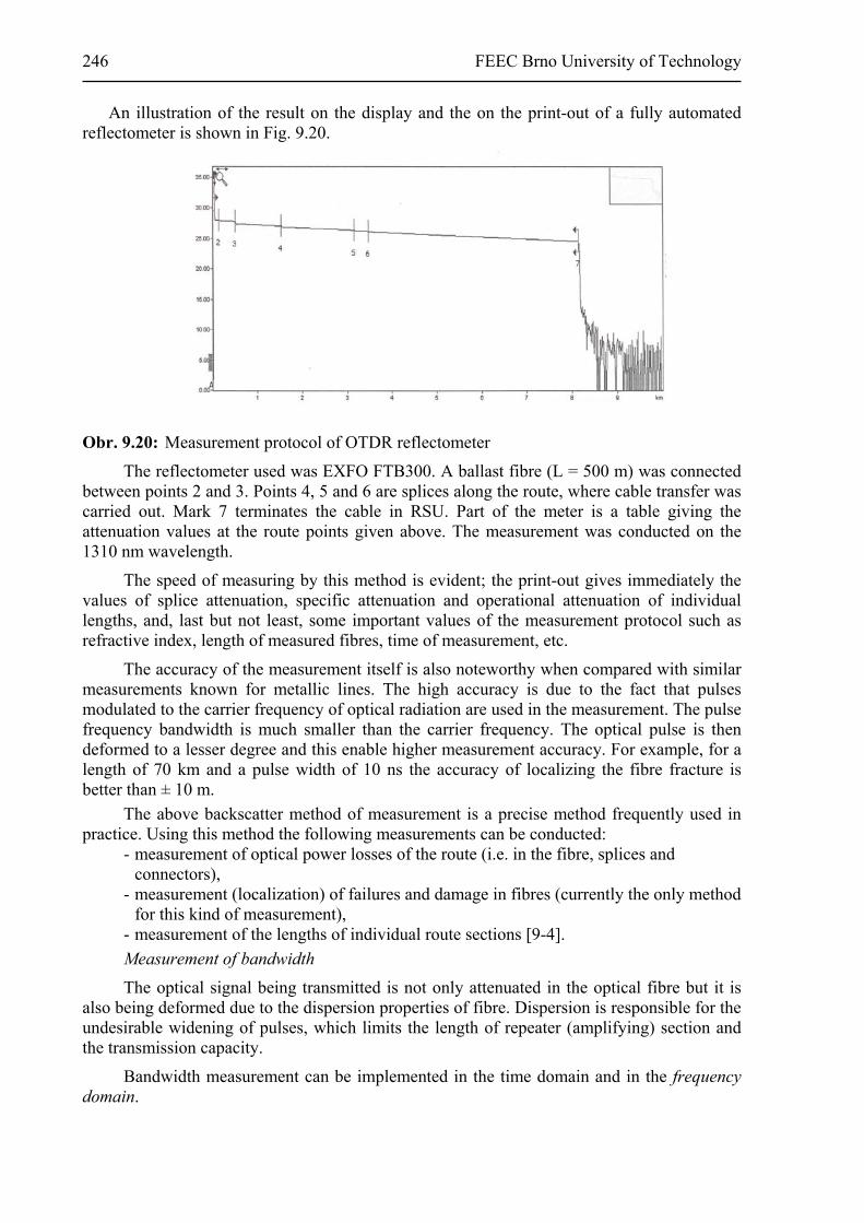
246 FEEC Brno University of Technology
An illustration of the result on the display and the on the print-out of a fully automated reflectometer is shown in Fig. 9.20.
Obr. 9.20: Measurement protocol of OTDR reflectometer
The reflectometer used was EXFO FTB300. A ballast fibre (L = 500 m) was connected between points 2 and 3. Points 4, 5 and 6 are splices along the route, where cable transfer was carried out. Mark 7 terminates the cable in RSU. Part of the meter is a table giving the attenuation values at the route points given above. The measurement was conducted on the 1310 nm wavelength.
The speed of measuring by this method is evident; the print-out gives immediately the values of splice attenuation, specific attenuation and operational attenuation of individual lengths, and, last but not least, some important values of the measurement protocol such as refractive index, length of measured fibres, time of measurement, etc.
The accuracy of the measurement itself is also noteworthy when compared with similar measurements known for metallic lines. The high accuracy is due to the fact that pulses modulated to the carrier frequency of optical radiation are used in the measurement. The pulse frequency bandwidth is much smaller than the carrier frequency. The optical pulse is then deformed to a lesser degree and this enable higher measurement accuracy. For example, for a length of 70 km and a pulse width of 10 ns the accuracy of localizing the fibre fracture is better than ± 10 m.
The above backscatter method of measurement is a precise method frequently used in practice. Using this method the following measurements can be conducted:
- measurement of optical power losses of the route (i.e. in the fibre, splices and connectors),
- measurement (localization) of failures and damage in fibres (currently the only method for this kind of measurement),
- measurement of the lengths of individual route sections [9-4].
Measurement of bandwidth
The optical signal being transmitted is not only attenuated in the optical fibre but it is also being deformed due to the dispersion properties of fibre. Dispersion is responsible for the undesirable widening of pulses, which limits the length of repeater (amplifying) section and the transmission capacity.
Bandwidth measurement can be implemented in the time domain and in the frequency domain.
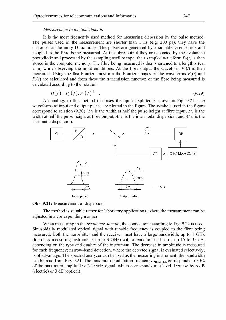
Optoelectronics for telecommunications and informatics 247
Measurement in the time domain
It is the most frequently used method for measuring dispersion by the pulse method. The pulses used in the measurement are shorter than 1 ns (e.g. 200 ps), they have the character of the unity Dirac pulse. The pulses are generated by a suitable laser source and coupled to the fibre being measured. At the fibre output they are detected by the avalanche photodiode and processed by the sampling oscilloscope; their sampled waveform P2(t) is then stored in the computer memory. The fibre being measured is then shortened to a length x (ca. 2 m) while observing the input conditions. At the fibre output the waveform P1(t) is then measured. Using the fast Fourier transform the Fourier images of the waveforms P1(t) and P2(t) are calculated and from these the transmission function of the fibre being measured is calculated according to the relation
.. 112
fPfPfH (9.29)
An analogy to this method that uses the optical splitter is shown in Fig. 9.21. The waveforms of input and output pulses are plotted in the figure. The symbols used in the figure correspond to relation (9.30) (2τ1 is the width at half the pulse height at fibre input, 2τ2 is the width at half the pulse height at fibre output, Δtvid is the intermodal dispersion, and Δtchr is the chromatic dispersion).
Obr. 9.21: Measurement of dispersion
The method is suitable rather for laboratory applications, where the measurement can be adjusted in a corresponding manner.
When measuring in the frequency domain, the connection according to Fig. 9.22 is used. Sinusoidally modulated optical signal with tunable frequency is coupled to the fibre being measured. Both the transmitter and the receiver must have a large bandwidth, up to 1 GHz (top-class measuring instruments up to 3 GHz) with attenuation that can span 15 to 35 dB, depending on the type and quality of the instrument. The decrease in amplitude is measured for each frequency; narrow-band detection, where the detected signal is evaluated selectively, is of advantage. The spectral analyzer can be used as the measuring instrument; the bandwidth can be read from Fig. 9.21. The maximum modulation frequency fmod max corresponds to 50% of the maximum amplitude of electric signal, which corresponds to a level decrease by 6 dB (electric) or 3 dB (optical).

248 FEEC Brno University of Technology
Obr. 9.22: Measurement of bandwidth
Obr. 9.23: Spectrum at fibre output
The mutual relation between dispersion Δt and bandwidth S = fmod max is given by the relation
-1
mod max
0, 44ns . km .t
f (9.30)
Measurement of chromatic dispersion
Method of phase shift and differential phase shift
By the ITU-T G.650 recommendation, the method of phase shift is given as the reference method for measuring the chromatic dispersion of optical fibres. A modulated radiation source of several wavelengths is used for the measurement. At the receiver side the instrument used for the detection of the test signal being received is an instrument for phase measurement such as the vector-voltmeter. The output phase measured is compared with the input phase of the signal and their difference is used to determine the change in the signal phase after the passage through the optical cable route being measured. A disadvantage of this method can be seen in the necessity to use a different fibre in the cable as the reference route in Fig. 9.24, via which information about the input phase is transmitted from the transmitter to the receiver.
Obr. 9.24: Method of phase shift

Optoelectronics for telecommunications and informatics 249
Method of delayed pulses in the time domain
This method consists in transmitting optical pulses in/on different wavelengths but with a precisely determined pulse magnitude and spacing. A comparison of the spacing of input pulses with that of the pulses received on the output is used to determine the delay due to chromatic dispersion. The connection which is similar to that in the preceding methods but without reference fibre is in Fig. 9.25.
Obr. 9.25: Method of delayed pulses
Fig. 9.26 gives an example of the connection of generator of optical pulses with given time spacing. A cascade of Bragg gratings serves as the monochromator. The pulse generator modulates the radiation of a wide-spectrum source such as LED diode. From the coming pulse the diode reflects components of selected wavelengths with certain time spacing back into the route being measured. The base is a cascade of Bragg gratings, which is formed by different gratings with sections of optical fibre between the gratings. Each of these gratings reflects radiation of different wavelength. The result of this connection is that a sequence of pulses of different wavelengths with given time spacing comes into the measured fibre of the route. After the passage through the route the time spacing of pulses changes due to the effect of chromatic dispersion. By comparing the spacing on the input with that on the output of the route being measured the values of delay due to chromatic dispersion are established.
Obr. 9.26: Method of delayed pulse, with a cascade of Bragg gratings
An example of the resultant measurement of optical route using a chromatic dispersion meter is given in Fig. 9.27 [9-5], [9-6].
Obr. 9.27: Waveform of chromatic dispersion

250 FEEC Brno University of Technology
Measurement of polarization mode dispersion (PMD)
The interferometric method of measuring PMD is based on the interference (wave addition) of low-coherence (coherence – spectral purity) of optical radiation. The block representation of the method is shown in Fig. 9.28. An interferometer is placed on the output of the optical route being measured, which separates the radiation into two branches. A fix mirror is in one branch and a movable mirror in the other branch. The movable mirror changes the phase shift between received signals of the two branches and, with the aid of interference, the delay due to PMD is shown on the detector.
Obr. 9.28: Measurement of PMD by interferometric method
A typical example of the plot obtained by this method is given in Fig. 9.29.
Obr. 9.29: Example of PMD plot of optical fibre, obtained by interferometric method
In the bottom of the figure the interferogram shows the correlation functions of two mutually perpendicular polarization planes. The pronounced peak is the autocorrelation function of the measuring signal itself, which depends on the shape of its spectrum.
This method is sometimes referred to as TINTY (Traditional Interferometry Analysis); the more recent method GINTY (General Interferometric Analysis) suppresses the effect of autocorrelation peak. In this method the resultant signal, which contains optical radiation from both branches of the interferometer, is again divided by polarization light into two mutually perpendicularly polarized components, with each of them incident on a separate detector. Interference occurs on the detectors and the two correlation components are expressed. By subtracting the interferogram we obtain the mutual correlation, and by adding up we obtain the pure autocorrelation. This method enables measuring also routes with EDFA amplifiers. It is a quick method, it is not necessary to measure individual route sections separately.
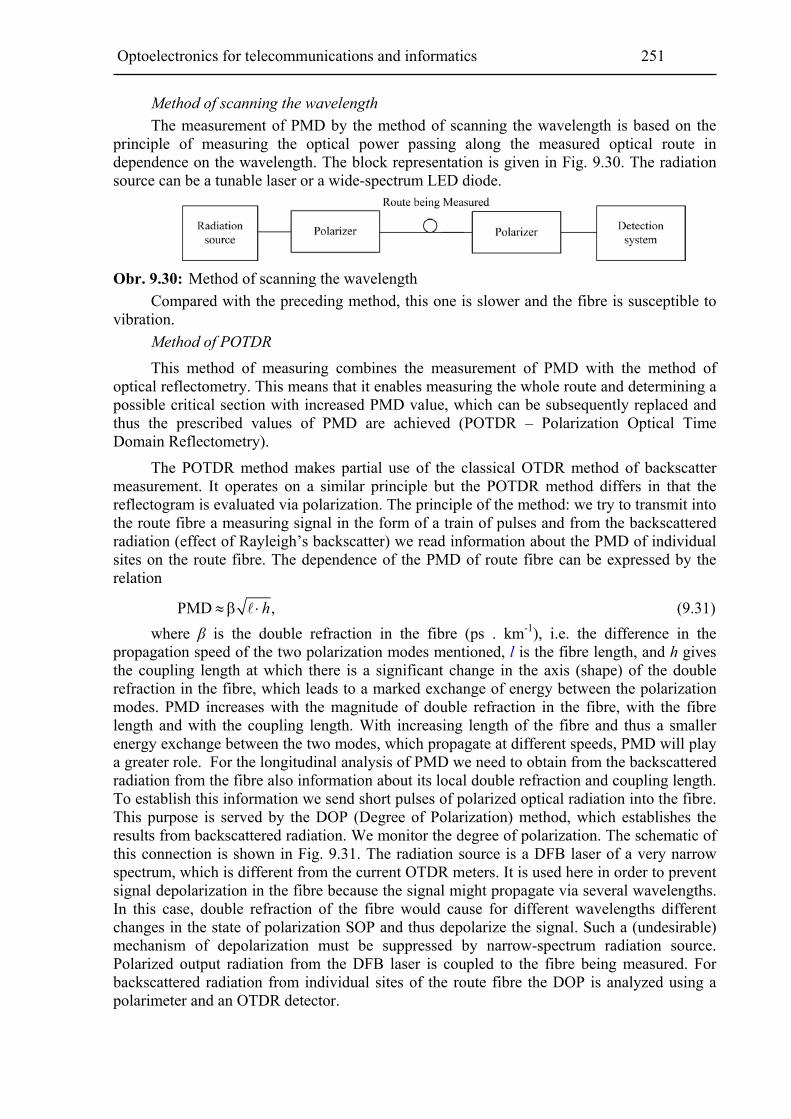
Optoelectronics for telecommunications and informatics 251
Method of scanning the wavelength
The measurement of PMD by the method of scanning the wavelength is based on the principle of measuring the optical power passing along the measured optical route in dependence on the wavelength. The block representation is given in Fig. 9.30. The radiation source can be a tunable laser or a wide-spectrum LED diode.
Obr. 9.30: Method of scanning the wavelength
Compared with the preceding method, this one is slower and the fibre is susceptible to vibration.
Method of POTDR
This method of measuring combines the measurement of PMD with the method of optical reflectometry. This means that it enables measuring the whole route and determining a possible critical section with increased PMD value, which can be subsequently replaced and thus the prescribed values of PMD are achieved (POTDR – Polarization Optical Time Domain Reflectometry).
The POTDR method makes partial use of the classical OTDR method of backscatter measurement. It operates on a similar principle but the POTDR method differs in that the reflectogram is evaluated via polarization. The principle of the method: we try to transmit into the route fibre a measuring signal in the form of a train of pulses and from the backscattered radiation (effect of Rayleigh’s backscatter) we read information about the PMD of individual sites on the route fibre. The dependence of the PMD of route fibre can be expressed by the relation
PMD ,h (9.31)
where β is the double refraction in the fibre (ps . km-1), i.e. the difference in the propagation speed of the two polarization modes mentioned, l is the fibre length, and h gives the coupling length at which there is a significant change in the axis (shape) of the double refraction in the fibre, which leads to a marked exchange of energy between the polarization modes. PMD increases with the magnitude of double refraction in the fibre, with the fibre length and with the coupling length. With increasing length of the fibre and thus a smaller energy exchange between the two modes, which propagate at different speeds, PMD will play a greater role. For the longitudinal analysis of PMD we need to obtain from the backscattered radiation from the fibre also information about its local double refraction and coupling length. To establish this information we send short pulses of polarized optical radiation into the fibre. This purpose is served by the DOP (Degree of Polarization) method, which establishes the results from backscattered radiation. We monitor the degree of polarization. The schematic of this connection is shown in Fig. 9.31. The radiation source is a DFB laser of a very narrow spectrum, which is different from the current OTDR meters. It is used here in order to prevent signal depolarization in the fibre because the signal might propagate via several wavelengths. In this case, double refraction of the fibre would cause for different wavelengths different changes in the state of polarization SOP and thus depolarize the signal. Such a (undesirable) mechanism of depolarization must be suppressed by narrow-spectrum radiation source. Polarized output radiation from the DFB laser is coupled to the fibre being measured. For backscattered radiation from individual sites of the route fibre the DOP is analyzed using a polarimeter and an OTDR detector.

252 FEEC Brno University of Technology
Obr. 9.31: Measurement of PMD by the method of DOP analysis
A strong double refraction in fibre β brings about a quick rotation of polarization state,
which leads to the depolarization of radiation within the measuring pulse, thus contributing to a reduction of the degree of polarization. A weak double refraction of fibre β will result in a high DOP measured, and vice versa. But the DOP will also depend on intermodal coupling (coupling length h). With some simplification, the situation can thus be divided into three groups:
1. fibres with weak double refraction (small β) – the DOP will be high (up to 1), irrespective of intermodal coupling. In practice, these are optical fibres with a small PMD value,
2. fibres with a strong double refraction and strong intermodal coupling (large β and short coupling length h) – the DOP will be low due to the strong double refraction (for a backscattered signal it will approximate the value 1/3) and will change rapidly due to the strong intermodal coupling. In practice, these are optical fibres with average PMD values,
3. fibres with a strong double refraction and weak intermodal coupling (large β and long coupling length h) – here, in addition to β and h, it also depends on the mutual position of SOP of polarization and on the shape of double refraction in the fibre. The DOP can then fluctuate between low and high values but it will change only slowly. In practice these are optical fibres with high PMD values.
It follows from the above that not only the DOP value itself but also the speed of DOP
change is important. The measuring instrument then performs an analysis of the results measured. Because of the considerable speed of DOP change it is first necessary to determine the average DOP value from several tens of samples. The measuring instrument then performs measurement for two states of input polarization, which yields two measurement results: DOP and DOPC (complementary), from which the DOPGEO parameter is calculated using the relation
,DOPDOPDOP 2C
2GEO (9.32)
which provides information about the real DOP value of radiation backscattered from a given section of route fibre. The measuring instrument has a parameter hDOP for monitoring the speed of DOP changes. This parameter is equal to the fibre length along which the DOP changes markedly – the quicker the DOP changes, the smaller the hDOP parameter. From an analysis of the DOP parameter of individual sections of optical fibre of route the following can be concluded:
- on sections with high DOPGEO value the PMD value will be low because the there is a small double refraction of fibre here,
Optoelectronics for telecommunications and informatics 253
- on sections with varying or low DOPGEO value and thus with a possible larger double refraction of fibre, and on the assumption that the hDOP parameter is
- small, then the PMD value will be low because there is a strong intermodal coupling in the fibre,
- average, then the PMD value will be average, - large, then the PMD value will be high because there is a weak intermodal coupling in
the fibre.
After the evaluation of the values measured, the polarization reflectogram (POTDR) will display several measurement results and graphs, above all the POTDR reflectogram, where individual cable sections and route sites can be followed. The longitudinal resolution power of this method is of the order of hundreds of metres; routes of tens of km in length can be measured. In the POTDR reflectogram display, sites with low, increased and high PMD values are presented in colour.
The second graphical representation that can be displayed is the waveform of the hDOP function, which is yet another important curve of the overall evaluation of PMD. In addition to the hDOP function, horizontal straight lines are also displayed, which mark the limit values of PMD. These limit values can be set by the users themselves.
The third (and most important) graphical representation is the DOP curve. In one graphical display several parameters can be seen in different colours – the DOP, DOPC and DOPGEO curves. The DOPGEO curve has the greatest informative value regarding the actual state of PMD.
The last possibility is the graphical representation of the curves (for both input states of POTDR polarization) of normalized Stokes parameters S1 to S3.
On top of all this, information about splice and connector sites can, of course, also be read from the final measurement protocol.
It is necessary to stress that the measurement of POTDR does not replace the total absolute values of PMD delay, which are measured using one of the interferometric methods, it only complements them.
9.5 Measurement of optoelectronic components
In our treatment so far we have had a source of radiation (LD or LED) on the input, photodiodes (PIN or APD) on the output, we have considered various passive elements, etc. and we have always assumed their failure-free operation with their intrinsic parameters. In many cases, however, it is necessary to establish the true parameters of these components, be it in connection with the manufacture or test measurement, etc.
One of the most important parameters of radiation sources is emitted power and its spectral characteristic. Optical power meters and optical spectrum analyzers are used to measure these parameters.
For measuring and checking detectors a corresponding radiation source is used together with a power meter or a selective meter.
The basic parameters of passive components (attenuation members, couplers, etc.) are insertion attenuation, directivity or division ratio. To measure these quantities, the same measuring facilities are necessary as for the measurement of attenuation of optical fibres, i.e. a stabilized radiation source and a meter of optical power.

254 FEEC Brno University of Technology
9.6 Special measurement methods
Included in this measurement category can be special laboratory measurements, research measurements, measurements with special measuring instruments, and single-purpose measurements.
Measurement with the application of spectral analyzer enables:
- measuring in a wide rage of wavelengths from 0.6 μm to 1.7 μm, depending on the structure of the elements used in the optical communication system, - a wide dynamic range for the measurement of wavelength attenuation characteristics and of the emitted spectrum of LED with a lens, - very accurate wavelength measurement with an accuracy of ± 1 nm, - measurement with high resolution power for LD, spectral measurement with an accuracy of ± 0.1 nm.
The measurement of optoelectronic telecommunication systems, in particular from the viewpoint of their development, concerns the measurement of optical power of transmission modules, the system reserve and the error rate. These measurements are performed using an optical power meter, which should be provided with probes of the measurement of the power of arbitrarily modulated optical signals and also the d.c. component.
In the measurement of the system reserve and system error rate a measuring optical attenuator is used, whose function is to simulate the optical route. It can be used with advantage to measure the linearity and sensitivity of detectors and receiver modules.
The measuring equipment for the installation and maintenance of optical track requires three basic measuring instruments: the backscatter meter (optical reflectometer) for the checking of the whole route, the optical power meter for the checking of the transmitting part, and the measuring optical attenuator for the checking of the receiving part.
Measurement of optical cable. In the course of cable installation the attenuation of individual fibres and attenuation of splices are measured using the backscatter meter. The meter is connected in the station where installation work starts. Attenuation is measured for all the fibres of each cable run before joining them to another run.
In the next step, attenuation of the splice of optical fibres of two manufacturing runs is measured. In this measurement the splice quality is the measure and if the attenuation is not low enough, the fibre splice must be made anew.
Attenuation and sometimes also dispersion are measured on an installed elementary section. Attenuation of splices is performed from the opposite end than in the case of splicing.
With an installed section, the fibre measurement is performed using an optical transmitter and receiver. At the beginning of the section the optical signal with already measured level P1 is introduced into the fibre. The input and output sides of the fibre are connected to the measuring instruments with connectors. Using a power meter the received level P2 is measured on the output. Optical attenuation of the fibre is given by the relation
L 2 1.A P P (9.33)
Each fibre is measured twice and the average of the two measurements is entered as value AL in the protocols. When the measurement is repeated, the transmitter is disconnected, its level is measured, and the receiver is also disconnected and then re-connected.
Measurement of splice attenuation in backward direction. This measurement is carried out after the installation of an elementary section from opposite direction to that in which the
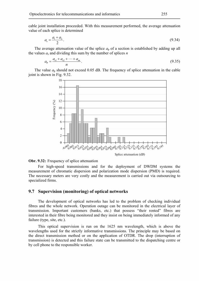
Optoelectronics for telecommunications and informatics 255
cable joint installation proceeded. With this measurement performed, the average attenuation value of each splice is determined
1 2s .
2
a aa
(9.34)
The average attenuation value of the splice ap of a section is established by adding up all the values as and dividing this sum by the number of splices n
s1 s2 snP .
a a aa
n
(9.35)
The value ap should not exceed 0.05 dB. The frequency of splice attenuation in the cable joint is shown in Fig. 9.32.
Obr. 9.32: Frequency of splice attenuation
For high-speed transmissions and for the deployment of DWDM systems the measurement of chromatic dispersion and polarization mode dispersion (PMD) is required. The necessary meters are very costly and the measurement is carried out via outsourcing to specialized firms.
9.7 Supervision (monitoring) of optical networks
The development of optical networks has led to the problem of checking individual fibres and the whole network. Operation outage can be monitored in the electrical layer of transmission. Important customers (banks, etc.) that possess “their rented” fibres are interested in their fibre being monitored and they insist on being immediately informed of any failure (type, site, etc.).
This optical supervision is run on the 1625 nm wavelength, which is above the wavelengths used for the strictly informative transmissions. The principle may be based on the direct transmission method or on the application of OTDR. The drop (interruption of transmission) is detected and this failure state can be transmitted to the dispatching centre or by cell phone to the responsible worker.
256 FEEC Brno University of Technology
The above methods can be combined. One of the registered and most elaborate systems on the market is the MLS (Monitoring Line System) system [9-7]. Details of this system, its characteristic, configuration, technical parameters, etc. are described in the literature.
10 Planar optical waveguides
The current rapid development of optoelectronic telecommunications is to a considerable extent limited by connections of the type of source-fibre-detector with their indispensable E/O and O/E conversions. In many cases this leads to very complicated solutions, where the effort concentrates on performing various functions such as splicing, switching, filtering, modulation, etc. in the optical region. Today, devices are being designed that enable combining different functions on a common substrate (slab). Implementations of this kind are of miniature dimensions and reliable, the time of optical signal passage through the complex of circuits is reduced, the power requirements (power supply) are lower, and the price is lower. Structures created in this way are (from the viewpoint of technology) commonly referred to as integrated optics (an analogy to integrated circuits in electronics). Planar optical waveguides form the basis of integrated optics.
Till now we have used optical fibres of circular cross-section to link up long sections but in integrated optics, where only short (centimeter) links are used, planar thin-layer waveguides are utilized [10-1], [10-2], [10-3].
10.1 Principle and fiction of planar lightquides
The simplest structure of a planar dielectric lightguide is shown in Fig. 10.1a. The structure is composed of three parts: substrate, dielectric layer itself, and surrounding medium (upper protection) with corresponding refractive indices ns, nf and np. Substances forming the structure should be non-absorbing and optically homogeneous. If the propagating wave is not limited because of the transverse dimensions of the waveguide, this waveguide is called two-dimensional waveguide. In this case the distribution of wave field is a function of only two variables (one transverse and one longitudinal, with respect to the direction of wave propagation). If the wave is limited in transverse direction, we obtain a three-dimensional waveguide. The three-dimensional waveguides are subdivided into strip and channel waveguides (see Fig. 10.1b). This strip or channels is usually deposited on the planar slab of optical material or created by diffusion right in the slab. Thanks to the well-tested technologies of thin layers, the manufacture of these waveguides is no problem.
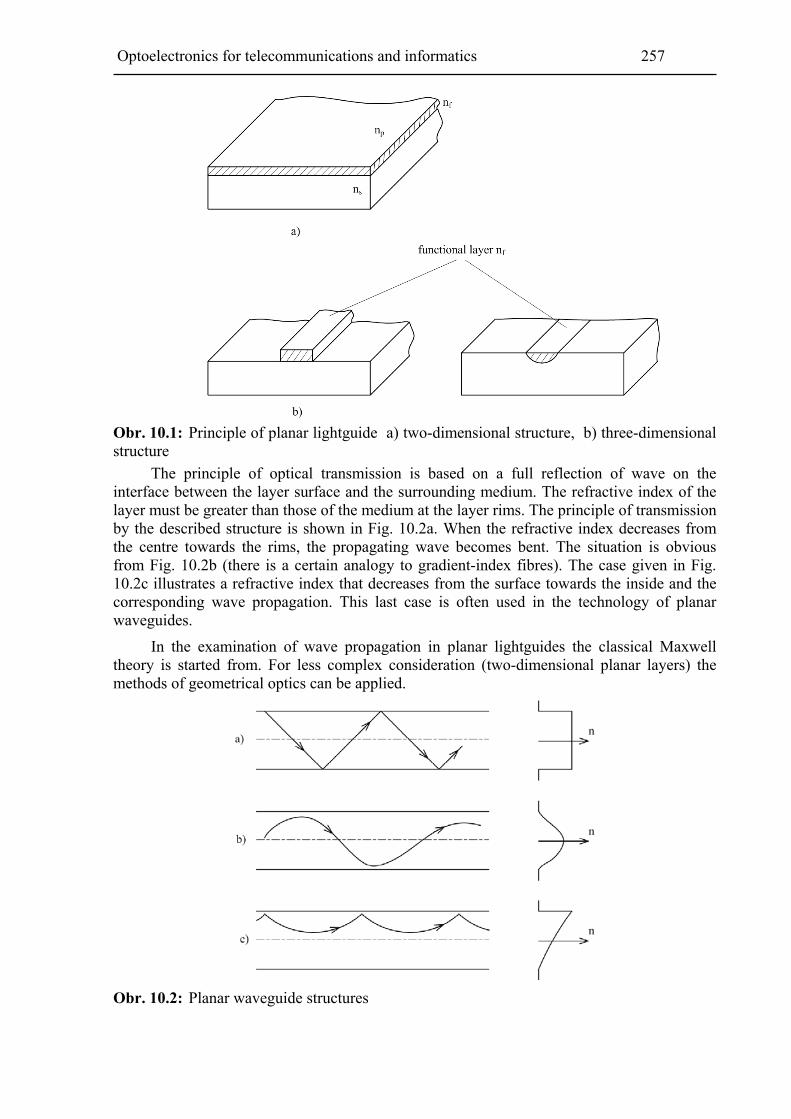
Optoelectronics for telecommunications and informatics 257
Obr. 10.1: Principle of planar lightguide a) two-dimensional structure, b) three-dimensional structure
The principle of optical transmission is based on a full reflection of wave on the interface between the layer surface and the surrounding medium. The refractive index of the layer must be greater than those of the medium at the layer rims. The principle of transmission by the described structure is shown in Fig. 10.2a. When the refractive index decreases from the centre towards the rims, the propagating wave becomes bent. The situation is obvious from Fig. 10.2b (there is a certain analogy to gradient-index fibres). The case given in Fig. 10.2c illustrates a refractive index that decreases from the surface towards the inside and the corresponding wave propagation. This last case is often used in the technology of planar waveguides.
In the examination of wave propagation in planar lightguides the classical Maxwell theory is started from. For less complex consideration (two-dimensional planar layers) the methods of geometrical optics can be applied.
Obr. 10.2: Planar waveguide structures
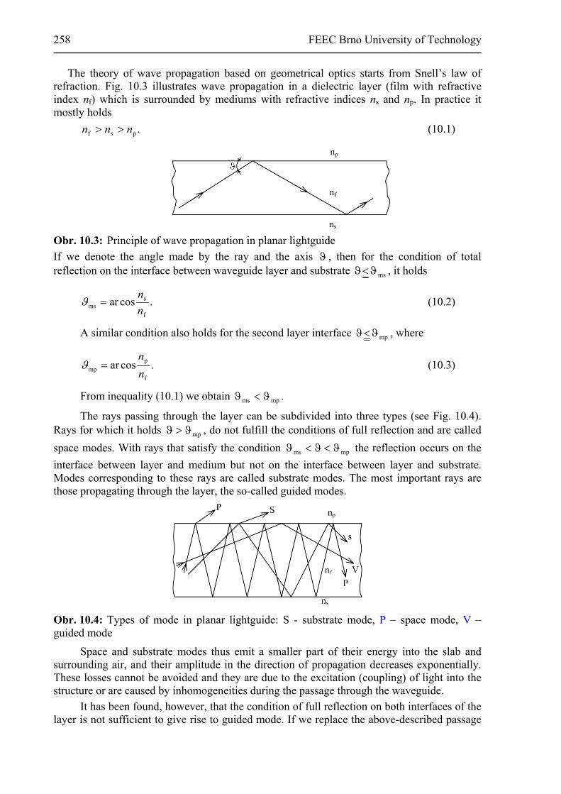
258 FEEC Brno University of Technology
The theory of wave propagation based on geometrical optics starts from Snell’s law of refraction. Fig. 10.3 illustrates wave propagation in a dielectric layer (film with refractive index nf) which is surrounded by mediums with refractive indices ns and np. In practice it mostly holds
.psf nnn (10.1)
Obr. 10.3: Principle of wave propagation in planar lightguide
If we denote the angle made by the ray and the axis , then for the condition of total reflection on the interface between waveguide layer and substrate ms , it holds
.cosarf
sms n
n (10.2)
A similar condition also holds for the second layer interface mp , where
.cosarf
pmp n
n (10.3)
From inequality (10.1) we obtain mpms .
The rays passing through the layer can be subdivided into three types (see Fig. 10.4). Rays for which it holds mp , do not fulfill the conditions of full reflection and are called
space modes. With rays that satisfy the condition mpms the reflection occurs on the
interface between layer and medium but not on the interface between layer and substrate. Modes corresponding to these rays are called substrate modes. The most important rays are those propagating through the layer, the so-called guided modes.
Obr. 10.4: Types of mode in planar lightguide: S - substrate mode, P – space mode, V – guided mode
Space and substrate modes thus emit a smaller part of their energy into the slab and surrounding air, and their amplitude in the direction of propagation decreases exponentially. These losses cannot be avoided and they are due to the excitation (coupling) of light into the structure or are caused by inhomogeneities during the passage through the waveguide.
It has been found, however, that the condition of full reflection on both interfaces of the layer is not sufficient to give rise to guided mode. If we replace the above-described passage

Optoelectronics for telecommunications and informatics 259
of light with two mutually perpendicular wave vectors it is not difficult to imagine the propagation of planar electromagnetic waves that will in different cases contain different non-zero components of electrical and magnetic fields. For the TE wave the components will be Ey, Hx and Hz while for the TH wave the components will be Hy, Ex and Ez.
The condition for the appearance of guided mode is that all the multiply reflected waves are added up in phase (and not cancelled). Consequently, the total phase change of planar wave with reflections from both interfaces must be 2πm, where m is an integer. It is thus easy to derive that only those waves (modes) can propagate through a dielectric layer that satisfy the condition
,222cosd2 fpfs1ff mΘkn (10.4)
where
2
ck is the wave number,
m is the order of the respective mode,
df is the layer thickness,
tpfs , are the phase changes for the reflection of optical wave of wavelength λ on
the interfaces functional layer/slab and functional layer/upper layer.
The field intensity waveform of these modes in the direction z can be expressed by the function exp(-iβz), where the propagation constant β is given by the relation
,sin 1f kNΘnk (10.5)
where N is the so-called effective refractive index of lightguide. For the purpose of practical evaluation of lightguide properties some quantities are
normalized. The most important among them are normalized frequency (thickness)
,21
2s
2ffn nndk (10.6)
measure of asymmetric structure
2s
2f
2c
2sn / nnnna (10.7)
and normalized refractive index of lightguide
./ 2s
2f
2s
2n nnnNb
The quantity an is mainly important in TE modes and its value is zero for perfect symmetry (ns = nc) and infinity for strong asymmetry fscs , nnnn . The maximum
value of quantity bn is 1, at the point of mode decay it is zero.
In the symmetrical type of lightguide there is no decay in mode guidance; in the aymmetric lightguide the decay begins at the value
.arctg 2/1nO a (10.8)
Where a greater transmission of modes is possible, the number of modes can be established from the relation
.2 2/12
s2f
fm nn
dN
(10.9)
The number of modes in a lightguide is basically a function of the thickness of active medium, of the difference between the refractive index of this medium and that of the slab or air.
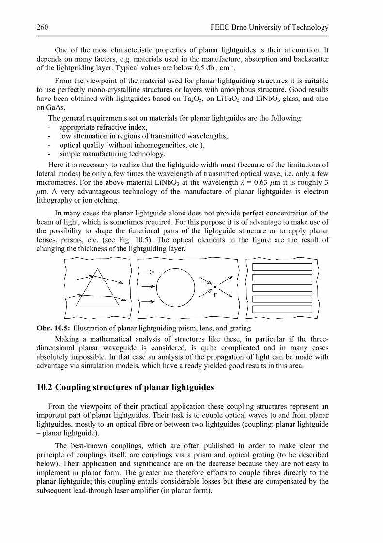
260 FEEC Brno University of Technology
One of the most characteristic properties of planar lightguides is their attenuation. It depends on many factors, e.g. materials used in the manufacture, absorption and backscatter of the lightguiding layer. Typical values are below 0.5 db . cm-1.
From the viewpoint of the material used for planar lightguiding structures it is suitable to use perfectly mono-crystalline structures or layers with amorphous structure. Good results have been obtained with lightguides based on Ta2O5, on LiTaO3 and LiNbO3 glass, and also on GaAs.
The general requirements set on materials for planar lightguides are the following: - appropriate refractive index, - low attenuation in regions of transmitted wavelengths, - optical quality (without inhomogeneities, etc.), - simple manufacturing technology.
Here it is necessary to realize that the lightguide width must (because of the limitations of lateral modes) be only a few times the wavelength of transmitted optical wave, i.e. only a few micrometres. For the above material LiNbO3 at the wavelength λ = 0.63 μm it is roughly 3 μm. A very advantageous technology of the manufacture of planar lightguides is electron lithography or ion etching.
In many cases the planar lightguide alone does not provide perfect concentration of the beam of light, which is sometimes required. For this purpose it is of advantage to make use of the possibility to shape the functional parts of the lightguide structure or to apply planar lenses, prisms, etc. (see Fig. 10.5). The optical elements in the figure are the result of changing the thickness of the lightguiding layer.
Obr. 10.5: Illustration of planar lightguiding prism, lens, and grating
Making a mathematical analysis of structures like these, in particular if the three-dimensional planar waveguide is considered, is quite complicated and in many cases absolutely impossible. In that case an analysis of the propagation of light can be made with advantage via simulation models, which have already yielded good results in this area.
10.2 Coupling structures of planar lightguides
From the viewpoint of their practical application these coupling structures represent an important part of planar lightguides. Their task is to couple optical waves to and from planar lightguides, mostly to an optical fibre or between two lightguides (coupling: planar lightguide – planar lightguide).
The best-known couplings, which are often published in order to make clear the principle of couplings itself, are couplings via a prism and optical grating (to be described below). Their application and significance are on the decrease because they are not easy to implement in planar form. The greater are therefore efforts to couple fibres directly to the planar lightguide; this coupling entails considerable losses but these are compensated by the subsequent lead-through laser amplifier (in planar form).

Optoelectronics for telecommunications and informatics 261
Prism coupling
Coupling via an optical prism enables a beam of light to be coupled (decoupled) from a radiant source to a planar lightguide, as shown in Fig. 10.6. There is a narrow air gap between the prism and the lightguide.
Obr. 10.6: Illustration of function of prism coupling component
The principle is based on a full reflection of optical wave traversing the prism on its base and exhausting power from the prism into the lightguiding layer, which happens when the propagation constants β in the prism and in the lightguides are equal. The strongest coupling occurs when the horizontal components of the wavelength vectors of the prism and the lightguides are equal; for a specific mode this always true for only one value of the angle of optical beam with respect to the plane of incidence.
For an efficient power transmission into the lightguide the following conditions must be satisfied [10-2]:
- refractive index of the layer forming the lightguide must be greater than the refractive index of the slab, i.e. n1 > n0,
- refractive index of the prism must be greater than the refractive index of the lightguiding layer, i.e. n3 > n1,
- distance between the prism base and the lightguide surface should be of the order of a tenth of wavelength λ (in the best case λ/8 to λ/4),
- constants of optical wave propagation in the prism and in the lightguide must be equal, i.e. it must hold
,sin30f Θnk (10.10)
where f is the constant of mode propagation in the layer,
k0 is the constant of optical wave propagation in vacuum /20k ,
Θ is the angle of optical beam propagation in the prism.
Coupling efficiency is somewhere about 80%; in some cases, when immersion liquid is used between the lightguide and the prism, efficiencies of over 90% have been achieved.
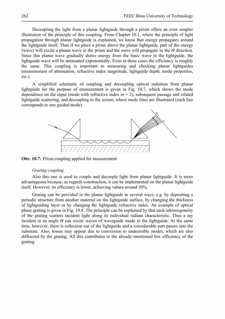
262 FEEC Brno University of Technology
Decoupling the light from a planar lightguide through a prism offers an even simpler illustration of the principle of this coupling. From Chapter 10.1, where the principle of light propagation through planar lightguide is explained, we know that energy propagates around the lightguide itself. Thus if we place a prism above the planar lightguide, part of the energy (wave) will excite a planar wave in the prism and the wave will propagate in the Θ direction. Since this planar wave gradually draws energy from the basic wave in the lightguide, the lightguide wave will be attenuated exponentially. Even in these cases the efficiency is roughly the same. This coupling is important in measuring and checking planar lightguides (measurement of attenuation, refractive index magnitude, lightguide depth, mode properties, etc.).
A simplified schematic of coupling and decoupling optical radiation from planar lightguide for the purpose of measurement is given in Fig. 10.7, which shows the mode dependence on the input (mode with refractive index m = 2), subsequent passage and related lightguide scattering, and decoupling to the screen, where mode lines are illustrated (each line corresponds to one guided mode).
Obr. 10.7: Prism coupling applied for measurement
Grating coupling
Also this one is used to couple and decouple light from planar lightguide. It is more advantageous because, as regards construction, it can be implemented on the planar lightguide itself. However, its efficiency is lower, achieving values around 30%.
Grating can be provided in the planar lightguide in several ways, e.g. by depositing a periodic structure from another material on the lightguide surface, by changing the thickness of lightguiding layer or by changing the lightguide refractive index. An example of optical phase grating is given in Fig. 10.8. The principle can be explained by that each inhomogeneity of the grating scatters incident light along its individual radiant characteristic. Thus a ray incident at an angle Θ can excite waves of waveguide mode in the lightguide. At the same time, however, there is reflection out of the lightguide and a considerable part passes into the substrate. Also, losses may appear due to conversion to undesirable modes, which are also diffracted by the grating. All this contributes to the already mentioned low efficiency of the grating.
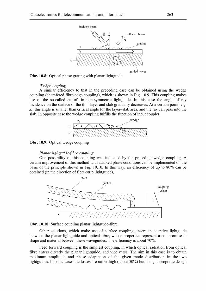
Optoelectronics for telecommunications and informatics 263
Obr. 10.8: Optical phase grating with planar lightguide
Wedge coupling A similar efficiency to that in the preceding case can be obtained using the wedge
coupling (chamfered fibre-edge coupling), which is shown in Fig. 10.9. This coupling makes use of the so-called cut-off in non-symmetric lightguide. In this case the angle of ray incidence on the surface of the thin layer and slab gradually decreases. At a certain point, e.g. xc, this angle is smaller than critical angle for the layer–slab area, and the ray can pass into the slab. In opposite case the wedge coupling fulfills the function of input coupler.
Obr. 10.9: Optical wedge coupling
Planar lightguide-fibre coupling One possibility of this coupling was indicated by the preceding wedge coupling. A
certain improvement of this method with adapted phase conditions can be implemented on the basis of the principle shown in Fig. 10.10. In this way, an efficiency of up to 80% can be obtained (in the direction of fibre-strip lightguide),
Obr. 10.10: Surface coupling planar lightguide-fibre
Other solutions, which make use of surface coupling, insert an adaptive lightguide between the planar lightguide and optical fibre, whose properties represent a compromise in shape and material between these waveguides. The efficiency is about 70%.
Feed forward coupling is the simplest coupling, in which optical radiation from optical fibre enters directly the planar lightguide, and vice versa. The aim in this case is to obtain maximum amplitude and phase adaptation of the given mode distribution in the two lightguides. In some cases the losses are rather high (about 50%) but using appropriate design

264 FEEC Brno University of Technology
adjustments they can be reduced (to a mere 10%). One possibility is to use lenses. Another possible method consists in making one end of the lightguide conic. There is also a method of V-grooves, which are obtained by etching in the silicon slab and ensure correct adjustment of the position of the fibre lightguide fronts with respect to the front of the strip planar lightguide.
Planar lightguide-planar lightguide coupling
This is a direct coupling of two planar lightguides; its efficiency depends primarily on a precise setting and adjustment of both ends of the lightguides to be coupled. An efficiency of up to 90% is obtained, depending on the kind of coupling structure. An example of this coupling is given in Fig. 10.11.
Obr. 10.11: Example of coupling two planar lightguides
10.3 Application of planar lightquides in integrated optics
Strip planar lightguides feature great potentials and methods for controlling passing coherent and incoherent optical radiation, i.e. directing, filtering, splitting, coupling and deviating it, al of this in a very small space, at a high speed of the operations carried out, and with little energy expended. As for the design, these circuits can be either implemented separately or be combined in optoelectronic chains and thus form design units based on a uniform structure and common technological processes. This gives rise to blocks of integrated optics ([10-4], [10-5], [10-6], etc.).
Also included among the currently used circuits of planar optics circuits and monolithic integrated optics can be hybrid integrated optical circuits, which employ both types of structure in combination with purely electronic processing.
A great advantage of planar optics is that it allows designing basic building elements such as sources, modulators, detectors with outputs to the planar lightguide, and combining them into integrated circuits.
Elements for optical signal distribution
These elements form the basis of the design of many members of planar optics that employ strip lightguides.
The basic elements include directional coupler, which is exhibited by every two dielectric waveguides brought so close together that their exponential fields blend together. Effective energy transmission is obtained only between such modes that have roughly the same propagation constant β. Then, in dependence on the difference of phase velocity of modes and on the local difference of the immediate phase of the propagating modes, the energy flows from one waveguide to another. By changing the mutual distances of coupled

Optoelectronics for telecommunications and informatics 265
waveguides or by changing the propagation conditions in one of the waveguides the mutual coupling can be efficiently spatially modulated and direction- or frequency-selective properties can thus be obtained. Fig. 10.12 gives examples of directional coupling.
Obr. 10.12: Examples of directional coupling a) mode synchronism b) selective couplings
Combining directional coupling with ring strip resonator enables the implementation of a highly selective narrow-band wavelength filter, see Fig. 10.13.
Obr. 10.13: Narrow-band resonance filter
Resonance properties are also a feature of structures using a profile planar or strip lightguide. Filters, resonance systems for coherent sources, and frequency multiplexers and demultiplexers can also be made.
Switch with four or eight leads can be implemented on a principle that is similar but more complicated from the viewpoint of manufacturing technology [10-5]. An example of four-lightguide switch is given in Fig. 10.14. The length of the whole switch is unbelievably small, a mere 2 mm. The optical beam either passes directly or deviates in the direction of the other lightguide..
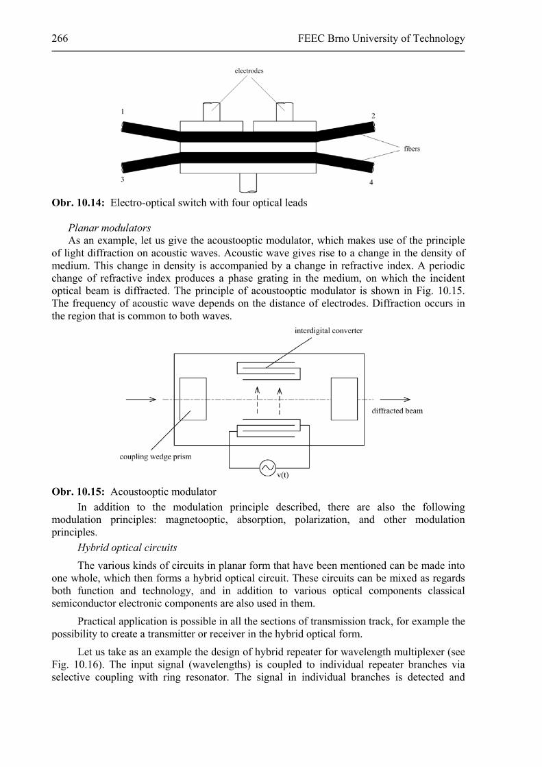
266 FEEC Brno University of Technology
Obr. 10.14: Electro-optical switch with four optical leads
Planar modulators As an example, let us give the acoustooptic modulator, which makes use of the principle
of light diffraction on acoustic waves. Acoustic wave gives rise to a change in the density of medium. This change in density is accompanied by a change in refractive index. A periodic change of refractive index produces a phase grating in the medium, on which the incident optical beam is diffracted. The principle of acoustooptic modulator is shown in Fig. 10.15. The frequency of acoustic wave depends on the distance of electrodes. Diffraction occurs in the region that is common to both waves.
Obr. 10.15: Acoustooptic modulator
In addition to the modulation principle described, there are also the following modulation principles: magnetooptic, absorption, polarization, and other modulation principles.
Hybrid optical circuits
The various kinds of circuits in planar form that have been mentioned can be made into one whole, which then forms a hybrid optical circuit. These circuits can be mixed as regards both function and technology, and in addition to various optical components classical semiconductor electronic components are also used in them.
Practical application is possible in all the sections of transmission track, for example the possibility to create a transmitter or receiver in the hybrid optical form.
Let us take as an example the design of hybrid repeater for wavelength multiplexer (see Fig. 10.16). The input signal (wavelengths) is coupled to individual repeater branches via selective coupling with ring resonator. The signal in individual branches is detected and

Optoelectronics for telecommunications and informatics 267
restored electronically. The regenerated electrical signal is then used to modulate the injection laser, and energy is coupled to the output lightguide.
Obr. 10.16: Hybrid repeater for wavelength multiplexer
By way of remark, let us mention the possibility to replace the repeater by an active planar lightguide with amplification. Its task is thus to amplify the passing light without the necessity of converting it to electrical signal. The application of these elements is limited: after two or at most three such amplifiers a classical repeater must be deployed.
It is evident that hybrid optical circuits have a promising future, in particular in view of the fact that for a long time the technology of classical electronics and that of coming optoelectronics will coexist. The hybrid technology can obviously be used to implement a whole range of necessary circuits for telecommunications.
Integrated optical circuits
These circuits make it possible to implement the earlier mentioned planar optical circuits in different combinations on a single chip. Similar to electronic integrated circuits, the task is to ensure a sufficiently high density of circuits per chip, high reliability, low price, etc. Because of their high electrooptical and acoustooptical coefficients, GaAs and GaAlAs are a suitable initial material for creating these structures. The suitability also holds from the viewpoint of technology with respect to easy epitaxy and possible implantation of electron or ion machining, etching, diffusion, etc.
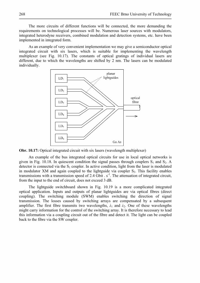
268 FEEC Brno University of Technology
The more circuits of different functions will be connected, the more demanding the requirements on technological processes will be. Numerous laser sources with modulators, integrated heterodyne receivers, combined modulation and detection systems, etc. have been implemented in integrated form.
As an example of very convenient implementation we may give a semiconductor optical integrated circuit with six lasers, which is suitable for implementing the wavelength multiplexer (see Fig. 10.17). The constants of optical gratings of individual lasers are different, due to which the wavelengths are shifted by 2 nm. The lasers can be modulated individually.
Obr. 10.17: Optical integrated circuit with six lasers (wavelength multiplexer)
An example of the bus integrated optical circuits for use in local optical networks is given in Fig. 10.18. In quiescent condition the signal passes through couplers S1 and S2. A detector is connected via the S1 coupler. In active condition, light from the laser is modulated in modulator XM and again coupled to the lightguide via coupler S2. This facility enables transmissions with a transmission speed of 2.4 Gbit . s-1. The attenuation of integrated circuit, from the input to the end of circuit, does not exceed 3 dB.
The lightguide switchboard shown in Fig. 10.19 is a more complicated integrated optical application. Inputs and outputs of planar lightguides are via optical fibres (direct coupling). The switching module (SWM) enables switching the direction of signal transmission. The losses caused by switching arrays are compensated by a subsequent amplifier. The first fibre transmits two wavelengths, λ1 and λ2. One of these wavelengths might carry information for the control of the switching array. It is therefore necessary to lead this information via a coupling circuit out of the fibre and detect it. The light can be coupled back to the fibre via the SW coupler.

Optoelectronics for telecommunications and informatics 269
Obr. 10.18: Integrated circuit of local optical network
The above illustrations of integrated optical networks give an idea of their technical applications and their merits. In the near future, they will certainly influence the design of optoelectronic transmission systems of large transmission capacities.
Obr. 10.19: Integrated switching optical circuit

270 FEEC Brno University of Technology
Conclusion The intent of this book has been to introduce the reader to the wide range of problems of
optoelectronics in telecommunications and informatics. The fundamental knowledge, state of the art, and potentials of this new field have been dealt with and its perspectives outlined.
In the introductory chapters the evolution of optoelectronics in telecommunications is given in brief, and the principles of transmission over this new medium are dealt with, including manufacture and installation. Attention is paid to the sources, modulation and detectors of light. The extent of the chapters was chosen such as to give the reader fundamental information. For a detailed study of these problems references are given to the respective literature that is available in this country.
The principal chapter is Chapter 8, which is concerned with optoelectronic telecommunication systems. Again within a limited extent, the wide range of use of optoelectronics for information transmission is mentioned. The titles of individual sub-chapters indicate the width of the problematic. It must be stressed, however, that only the essentials of individual problems are given; for in-depth knowledge it is again necessary to refer to the literature or to use other sources, preferably journals and web pages, which usually bring the latest scientific knowledge. In this respect, it is also good to bear in mind the long stretch of time between writing a book and publishing it. This is particularly appreciable in such a rapidly developing field as optoelectronics.
Chapter 9 is devoted to problems of measurement, without which the installation and operation of optoelectronic telecommunication systems are hard to imagine. The last chapter, Chapter 10, gives an introduction to problems of planar lightguides and integrated optoelectronics with focus on information transmission. The aim of the above division of book content is to provide the reader with a good overview of optoelectronics as applied in telecommunications and informatics. The book has been conceived such that in addition to being used as university texts it should also serve secondary-school and other workers interested in this new problematic.
The book should contribute to the current development of digital technology, further development and introduction of optoelectronics in the Czech telecommunication network, development of FTTx networks, FTTH in particular. The suggested path is a path in the direction of advances in telecommunications and informatics, and in society as such.
Although the book deals with a wide range of problems, it is necessary at this point to at least indicate further optoelectronics applications, which in a few years’ time will have an impact on telecommunications and informatics. This concerns primarily various digital signal processors, techniques of controlling single-mode transmission of radiation in strip and planar lightguides, making use of the principle of the interference of coherent beams, the principle of controlling the coupling of two lightguides, the principle of radiation diffraction on sound or mechanical grating, etc. Optical integrated processors enable performing a number of complex functions and processing both analogue and digital signals (analogy of electronic integrated circuits). Their speed of operation is several orders beyond the potentials of electronic integrated circuits.
Interesting scientific knowledge can be obtained from holography, which is basically a special method of recording and displaying three-dimensional objects. Computer storage systems are being developed on these principles.

Optoelectronics for telecommunications and informatics 271
Another wide area optpelectronics is the area of sensors. In telecommunications, the area of application is in the first place the solution of microtelephone receiver insets, switches, etc.
Optoelectronics is also used in ranging and range-finder systems.
Optoelectronics also finds application in transport, power engineering, medicine, commerce, army, instruction, etc.
In spite of all this success, the largest optoelectronics market is in telecommunications and informatics. The development of telecommunications and transmission of information are today unthinkable without optical fibres. Interest in optical fibres will continue to rise with their decreasing price. Provided attenuation can further be reduced, an era of plastic fibres may come. This would mean a “revolution” in optical transmission, primarily because of low prices and simple installation.
This advance will further be enhanced by prospective reduction of attenuation of optical fibres, splices, and connectors. Transmission of information over still larger distances without repeaters will be made possible.
Let us state in conclusion that in present-day and future telecommunications and informatics, i.e. in optoelectronics, the copper wire is not and will not be “dead” for a long time.

272 FEEC Brno University of Technology
References [ 1-1 ] KAO, C. – HOCKHAM, G. A. Dielectric Fibre Surface Wave-guides for Optical
Frequencies. IEEE, 1976, č.7.
[ 1-2 ] ŠAVEL, J. a kol. Přenos informací na optických kmitočtech. SNTL, Praha, 1982.
[ 1-3 ] ITU-T, G652, G653, G641. Ženeva, 1995.
[ 2-1 ] MAHLKE, G. Fiber Optic Cables. Siemens, München, 1997.
[ 2-2 ] FILKA, M. Přenosová média. Skripta VUT FEKT, Brno, 2003.
[ 2-3 ] SOCHOR, V. Optické, elektrodynamické a nelineární vlastnosti optických vláken. Academia, Praha, 1986.
[ 2-4 ] DAVID, I. Výběr optického vlákna. Telekomunikace 1998, č.10.
[ 2-5 ] KOČ, Z. Optická vlákna v telekomunikacích. Sdělovací technika, 1999, č.3.
[ 2-6 ] GUO, Y., KAO, K.C., Li, H.E., CHINAG K.S. Non-linear Photonics. Springer, New York, 2003.
[ 2-7 ] DAUM, W., KRAUSER, J., ZAMZOV, P., ZIEMANN, O. POF, Polymer Optical Fibers for Data Communication. Springer, Berlin, 2001.
[ 2-8 ] THORLABS. Catalog Volume 19. Thorlabs, Sweden, 2006.
[ 2-9 ] SCHRÖFEL, J., NOVOTNÝ, J. Optické vlnovody. SNTL, Praha, 1986.
[ 2-10] PETERKA, P., KAŠÍK, I., MATĚJEC, V. Optimální tvar průřezu vlákna pro pláště čerpané vláknové lasery a zesilovače. In. Sborník Optické komunikace, OK 2003. Praha, Agentura Action M, 2003.
[ 2-11] Firemní sborník THOR LABS. New York 2007.
[ 2-12] Firemní sborník OPTOKON. Jihlava 2007.
[2-13] HONZÁTKO, P., KAŇKA, J., MATĚJEC, V. Mikrostrukturní optická vlákna. In. Sborník Optické komunikace, OK 2002. Praha, Tech-Martek 2002.
[2-14] www.optokon.cz
[2-15] www.asm.cz
[ 3-1 ] MILLER, E.S., CHYNOWTH, A.G. Optical Fiber Telecommunications. Academic Press, London, 1979.
[ 3-2 ] MAHLKE, G. Fiber Optic Cables. Siemens, München, 1997.
[ 3-3 ] PLAVAK, M., KOVÁTS, K. Optické vlákna a káble. VUKI, Bratislava, 1992.
[ 4-1 ] MAHLKE, G. Fiber Optic Cables. Siemens, München, 1997.
[ 4-2 ] Firemní dokumentace KABELOVNA Děčín-Podmokly, 2000.
[ 4-3 ] Firemní dokumentace, SQS, 2000.
[ 4-4 ] www.belden.com
[ 4-5 ] www.kassex.cz
[ 4-6 ] www.ampnetconnect.cz
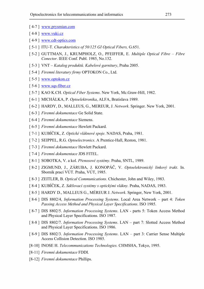
Optoelectronics for telecommunications and informatics 273
[ 4-7 ] www.prysmian.com
[ 4-8 ] www.vuki.cz
[ 4-9 ] www.cdt-optics.com
[ 5-1 ] ITU-T. Charakteristics of 50/125 GI Optical Fibers, G.651.
[ 5-2 ] GUTTMAN, J., KRUMPHOLZ, O., PFEIFFER, E. Multiple Optical Fibre – Fibre Conector. IEEE Conf. Publ. 1985, No.132.
[ 5-3 ] VNT – Katalog produktů. Kabelové garnitury, Praha 2005.
[ 5-4 ] Firemní literatury firmy OPTOKON Co., Ltd.
[ 5-5 ] www.optokon.cz
[ 5-6 ] www.sqs-fiber.cz
[ 5-7 ] KAO K.CH. Optical Fiber Systems. New York, Mc.Graw-Hill, 1982.
[ 6-1 ] MICHÁLKA, P. Optoelektronika, ALFA, Bratislava 1989.
[ 6-2 ] HARDY, D., MALLEUS, G., MEREUR, J. Network. Springer. New York, 2001.
[ 6-3 ] Firemní dokumentace Ge Solid State.
[ 6-4 ] Firemní dokumentace Siemens.
[ 6-5 ] Firemní dokumentace Hewlett Packard.
[ 7-1 ] KUBÍČEK, Z. Optické vláknové spoje. NADAS, Praha, 1981.
[ 7-2 ] SEIPPEL, R.G. Optoelectronics. A Prentice-Hall, Reston, 1981.
[ 7-3 ] Firemní dokumentace Hewlett Packard.
[ 7-4 ] Firemní dokumentace JDS FITEL.
[ 8-1 ] SOBOTKA, V. a kol. Přenosové systémy. Praha, SNTL, 1989.
[ 8-2 ] ZIGMUND, J., ZÁRUBA, J. KONOPÁČ, V. Optoelektronický linkový trakt. In. Sborník prací VÚT. Praha, VÚT, 1985.
[ 8-3 ] ZEITLER, B. Optical Communications. Chichester, John and Wiley, 1983.
[ 8-4 ] KUBÍČEK, Z. Sdělovací systémy s optickými vlákny. Praha, NADAS, 1983.
[ 8-5 ] HARDY D., MALLEUS G., MÉREUR J. Network. Springer, New York, 2001.
[ 8-6 ] DIS 8802/4, Information Processing Systems. Local Area Network – part 4: Token Passing Access Method and Physical Layer Specifications. ISO 1985.
[ 8-7 ] DIS 8802/5. Information Processing Systems. LAN - parts 5: Token Access Method and Physical Layer Specifications. ISO 1987.
[ 8-8 ] DIS 8802/7. Information Processing Systems. LAN – part 7: Slotted Access Method and Physical Layer Specifications. ISO 1986.
[ 8-9 ] DIS 8802/3. Information Processing Systems. LAN – part 3: Carrier Sense Multiple Access Collision Detection. ISO 1985.
[8-10] INOSE H. Telecommunications Technologies. CHMSHA, Tokyo, 1995.
[8-11] Firemní dokumentace FDDI.
[8-12] Firemní dokumentace Phillips.

274 FEEC Brno University of Technology
[8-13] GIRARD, A. FTTx PON, Technology and Testing. EXFO, Quebec, 2005.
[8-14] Firemní dokumentace FTTx Pon Guide. EXFO, Quebec, 2006.
[8-15] GIRARD, A. Guide to WDM Technology. EXFO, Quebec, 2002.
[8-16] HARDY, D., MALLEUS, G., MÉREUR, J. Network. Springer, New York, 2001.
[8-17] KARÁSEK, M., VOJTĚCH, J., RADIL, J. Obousměrný přenos 8 x 10GE přes 210 km standardního jednovidového vlákna bez linkového EDFA. In. Optické komunikace 2006. Action M, Praha, 2006.
[8-18] Firemní dokumentace MCS, Siemens.
[8-19] Firemní literatura, JDS FITEL, 2002.
[8-20] Firemní literatura, SQS, 2002.
[8-21] KONTROLSKIJ, I.P. Osnovy infrakrasnoj technikyI. NEI, Moskva, 1986.
[8-22] ČEKAN, V. Využití infračerveného záření pro přenos nf.signálu v uzavřených prostorech. Kandidátská disertace. VUT FEI, Brno 1988.
[8-23] WILFERT, O., KOLKA, Z., BIOLKOVÁ, V. Optická komunikace volným prostorem. In. Optické komunikace 2004. Agentura Action M, Praha 2004.
[8-24] SCHRÖDER, G. Technická optika. SNTL, Praha 1981.
[8-25] VAŠÍČEK, A. Optika tenkých vrstev. Praha, ČSAV 1986.
[8-26] DADO, M. Optoelektronika v telekomunikacích. Skripta. VŠDS, Žilina 1989.
[8-27] FILOVÁ, A., KAŠÁK, J. In. Návrh interferenčního filtru pro optický přenosový systém. Vědecké práce. VŠDS, Žilina 1988.
[8-28] DADO, M. a kol. Kapitoly z optiky pre technikov. EDIS, Žilina 1998.
[8-29] Firemní literatura, AOC TEL, 2006.
[8-30] DOSTÁL, O., FILKA, M., PETRENKO, M. First Experiences with Picture Archiving and Communication Systese in Medicine. In. Proceedings VIProm. ELMAR, Zadar, Croatia, 2002, ISBN 953-7044-01-7.
[8-31] Medicínské aplikace. Závěrečné výzkumné zprávy. Brno, ÚVT MU 2001.
[8-32] SCHMIDT, M., DOSTÁL, O., JAVORNÍK, M. MEDIMED – Regional PACS Centre in Brno. Ing EuroPACS – MIR 2004. Trieste-Italy: University of Trieste, 2004, od s.463-465. ISBN 88-8303-150-4.
[8-33] KEFURT, P. Mapový průvodce českým Internetem. Sdělovací technika, 2004.
[8-34] www.security.cz
[8-35] www.safibra.cz
[8-36] www.humusoft.cz
[8-37] HÁJEK, M., HOLOMEČEK, P. Praktické zkušenosti z měření DWDM. www.mikrokom.cz/pdf/zkusenosti-merDWDM.pdf
[8-38] GRUNTORÁD, J. Průběžná zpráva o řešení výzkumného záměru v roce 2005 [PDF dokument]. Dostupný na http://www.cesnet.cz/doc/zprava2005/
Optoelectronics for telecommunications and informatics 275
[8-39] ŠMEJKAL, K. Optické spoje v metropolitní síti. Sborník abstraktů, konference Vysokorychlostní sítě 2004. [PDF dokument]. Dostupný na http://www.vrs.pasnet.cz/vrs2004/Sbornik_vrs2004.pdf
[8-40] ITU-T Recommendation G.671: Transmission characteristics of optical components and subsystems. ITU-T, 06/2002.
[8-41] KYSELÁK, M.: Optimalizace vysokorychlostních optických přenosových tras [on-line]. Dostupný na http://www.elektrorevue.cz/clanky/06009/
[8-42] ITU-T Recommendation G.652: Characteristics of a single-mode optical fibre cable. ITU-T, 06/2005.
[8-43] ITU-T Recommendation G.653: Characteristics of a dispersion-shifted single-mode optical fibre cable. ITU-T, 06/2005.
[8-44] ITU-T Recommendation G.654: Characteristics of a cut-off shifted single-mode optical fibre and cable. ITU-T, 06/2004.
[8-45] ITU-T Recommendation G.655: Characteristics of a non-zero dispersion shifted single-mode optical fibre cable. ITU-T, 03/2006.
[8-46] ITU-T Recommendation G.656: Characteristics of a fibre and cable with non-zero dispersion for wideband optical transport. ITU-T, 06/2004.
[ 9-1 ] ŠVITORKA, Z. Úvod do problematiky měření na optických traktech. In. Měření a údržba sdělovacích kabelů. Tábor, ČSVTS, 1985.
[ 9-2 ] SCHLITTER, M., HUBIČKA, V. Sdělovací vedení. Skriptum. Praha, ČVUT, 1985.
[ 9-3 ] KUCHARSKI, M., DUBSKY, P. Měření přenosových parametrů optických vláken, kabelů a tras. Mikrokom, Praha, 2001.
[ 9-4 ] Firemní dokumentace EXFO FTB 300. EXFO, Quebec, 2002.
[ 9-5 ] Firemní dokumentace EXFO, Quebec, 2000.
[ 9-6 ] www.exfo.com
[ 9-7 ] www.sqs.fiber.cz
[10-1] ČTYROKÝ, J. Integrovaná optika. Praha, SNTL, 1986.
[10-2] ŠAVEL, J. a kol. Přenos informací na optických kmitočtech. Praha, SNTL, 1982.
[10-3] SCHRÖFEL, J., NOVOTNÝ, K. Optické vlnovody. Praha, SNTL, 1986.
[10-4] Firemní dokumentace Laser Components, 2001.
[10-5] Firemní dokumentace JDS FITEL, 2000.
[10-6] Firemní dokumentace Hewlett Packard, 1999.