Optoelectronic Materials: Transparent Conductors, Light Emittersth.fhi-berlin.mpg.de › sitesub ›...
40
Chris G. Van de Walle Materials Department, University of California, Santa Barbara with Cyrus Dreyer, Anderson Janotti, Hartwin Peelaers Audrius Alkauskas (Ctr. f. Physical Sciences and Technology, Lithuania) J. L. Lyons (Brookhaven National Lab.) Qimin Yan (Lawrence Berkeley National Lab.) Patrick Rinke (Aalto U.) Emmanouil Kioupakis (U. Michigan) Acknowledgments: NSF, DOE, ARO, ONR; XSEDE, NERSC Optoelectronic Materials: Transparent Conductors, Light Emitters Density Functional Theory and Beyond Berlin, July 21, 2015
Transcript of Optoelectronic Materials: Transparent Conductors, Light Emittersth.fhi-berlin.mpg.de › sitesub ›...

Chris G. Van de WalleMaterials Department, University of California, Santa Barbara
withCyrus Dreyer, Anderson Janotti, Hartwin PeelaersAudrius Alkauskas (Ctr. f. Physical Sciences and Technology, Lithuania)J. L. Lyons (Brookhaven National Lab.)Qimin Yan (Lawrence Berkeley National Lab.)Patrick Rinke (Aalto U.)Emmanouil Kioupakis (U. Michigan)
Acknowledgments: NSF, DOE, ARO, ONR; XSEDE, NERSC
Optoelectronic Materials:Transparent Conductors,
Light Emitters
Density Functional Theory and BeyondBerlin, July 21, 2015

Transparent conducting oxidesTransparent conducting oxides (TCOs) have many applications
Contacts in solar cells
Touchscreens
Electrodes in LCD screens
Smart windows
Possible because materials combine‐ transparency‐ conductivity

Absorption processes
Direct valence‐ to conduction‐band transition→ band gap is 3.6 eV (344 nm)→ no absorp on in visible range (even into the UV)
SnO2
Example:

Absorption processes
Direct transition between conduction bands:→ first to second conduc on band: 4.7 eV (262 nm)→ also not in visible range
SnO2
Absorption processes
Indirect transition:conduction band to conduction band
SnO2

Absorption processes
Indirect transition:→ requires addi onal momentum: e.g., from phonons
O en described by Drude model → phenomenological
SnO2

Theoretical descriptionAbsorption coefficient Fermi’s golden rule
The + signs indicates phonon emission, the – sign phonon absorption.
No fi ng parameters! → predic ve!
Delta function: conservation of energy

Computational details: SnO2
• Norm-conserving pseudopotentials• Plane-wave basis• Local Density Approximation (LDA)• Density functional perturbation theory (DFPT) to obtain phonons• Absorption calculated at 300K
SnO
c
Focus on SnO2(techniques are general)
SnO2: ‐ rutile structure‐ 6 atoms/unit cell
c direction important

Absorption spectrum
Linear on log‐log scale
Over large rangeof wavelengths:
power law!
Deviation for wavelengths < 450 nm
InfraredUV

Absorption < 450 nm
→ absorp on due to states near the band edges
CB DOS
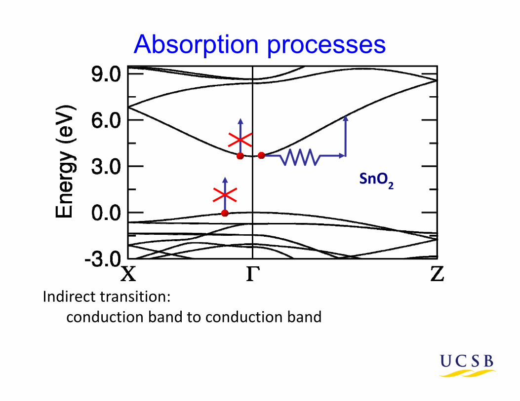
Contributions to absorption @ 300K
Emission of phonons is biggest contribution → possible even at low temperatures
Fundamental limit!
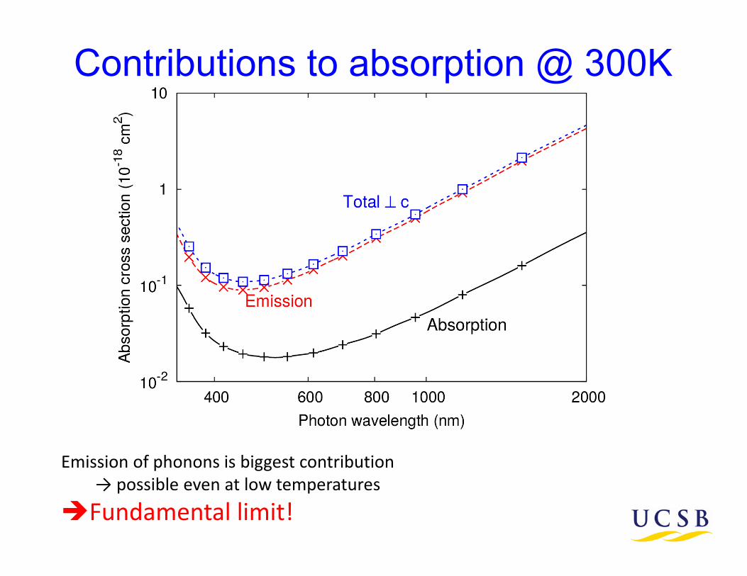
Fröhlich versus first principles
Similar power law for large wavelengths, but completely misses increase < 450 nm
→ Fröhlich only captures intraband transi ons

Importance of LO modes
For large wavelengths: LO mode is dominant Small wavelengths: other modes become important→ defines region Fröhlich model can be used
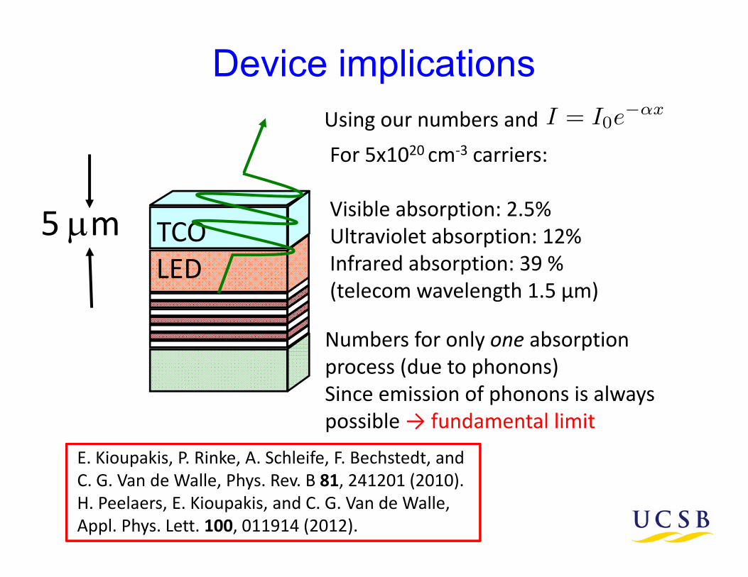
Device implications
5 m TCOLED
For 5x1020 cm‐3 carriers:
Visible absorption: 2.5%Ultraviolet absorption: 12%Infrared absorption: 39 % (telecom wavelength 1.5 μm)
Using our numbers and
Numbers for only one absorption process (due to phonons)Since emission of phonons is always possible → fundamental limit
E. Kioupakis, P. Rinke, A. Schleife, F. Bechstedt, and C. G. Van de Walle, Phys. Rev. B 81, 241201 (2010). H. Peelaers, E. Kioupakis, and C. G. Van de Walle, Appl. Phys. Lett. 100, 011914 (2012).

LEDs for solid‐state lighting
15
UCSB SSLEC, 2012
Cree.com

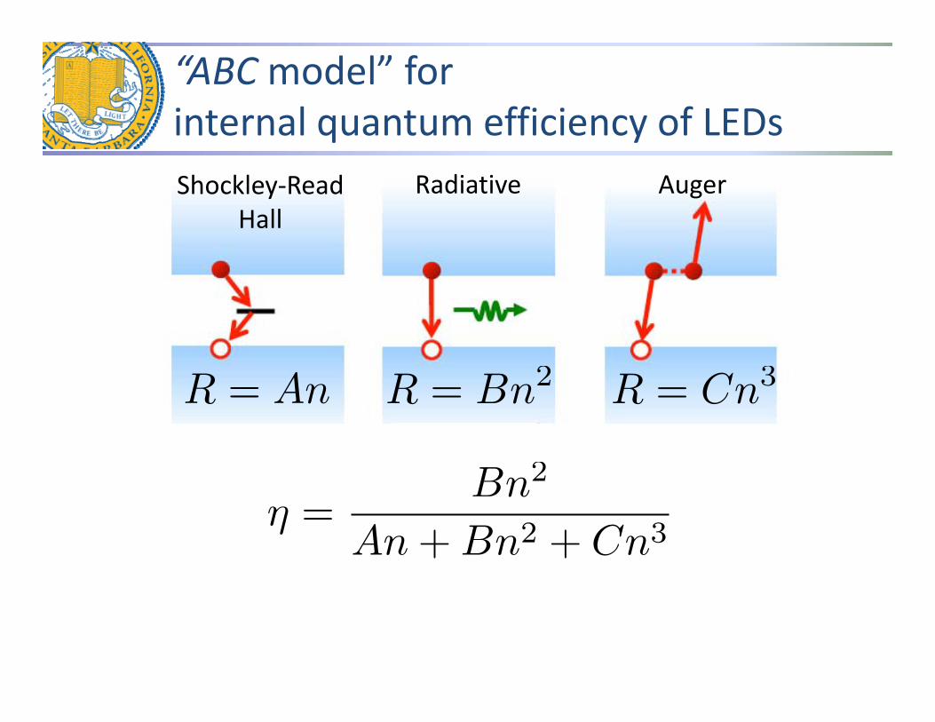
“ABCmodel” for internal quantum efficiency of LEDs
AugerShockley‐Read Hall
Radiative
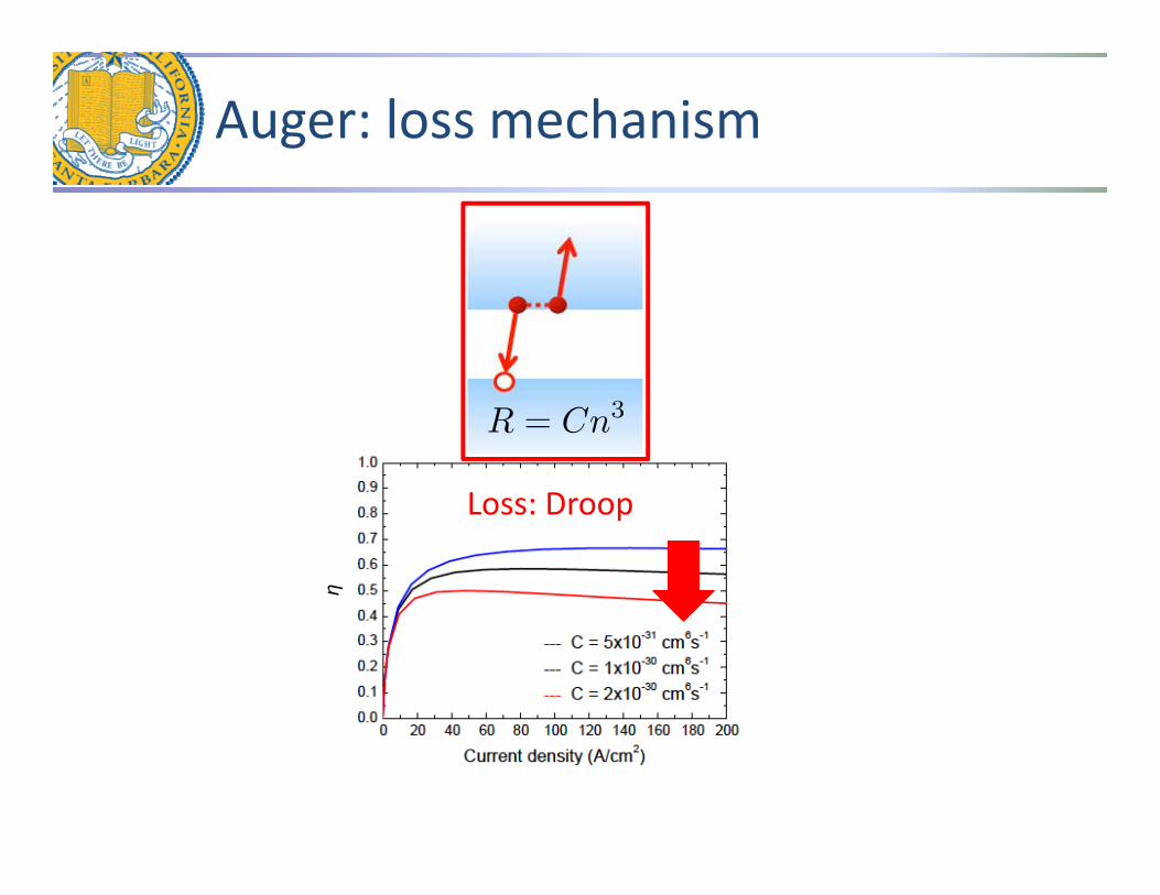
Loss: Droop
Auger: loss mechanism
η

Direct & Indirect Auger recombination
Carrier scattering by:
+
Electron‐phonon Alloy scattering Charged defects
Direct Auger Indirect Auger
Bulashevich & Karpov, pssc (2008)

Indirect Auger recombination
Atomic-scale calculations from first principles, explicitly study microscopic scattering mechanisms
• Electrons: local density approximation+scissors operator• Phonons: density functional perturbation theory• Dielectric function: G. Cappellini et al., PRB 1993

Calculating the Auger coefficient
• Conserve momentum, eliminate k4-sum 9D integral
• δ Gaussian, vary band gap
• Sampling of k1,k2,k3 on grid
• Generate all k4 = k1+k2–k3, pre-calculate wave functions
• #k1,k2,k3 10-100, #k4 1,000-5,000
• Parallel Auger code, biggest run ~3,000 CPUs for 4h

Auger Recombination in GaN and InGaN
Phononassisted
E. Kioupakis, P. Rinke, K. T. Delaney, and C. G. Van de Walle, Appl. Phys. Lett. 98, 161107 (2011).E. Kioupakis, D. Steiauf, P. Rinke, K. T. Delaney, and C. G. Van de Walle, Phys. Rev. B (in press).

The Smoking Gun: Direct observation of Auger electrons

Short‐range scattering
Need to model short-range scattering and bands at edge of BZ:First-principles theory
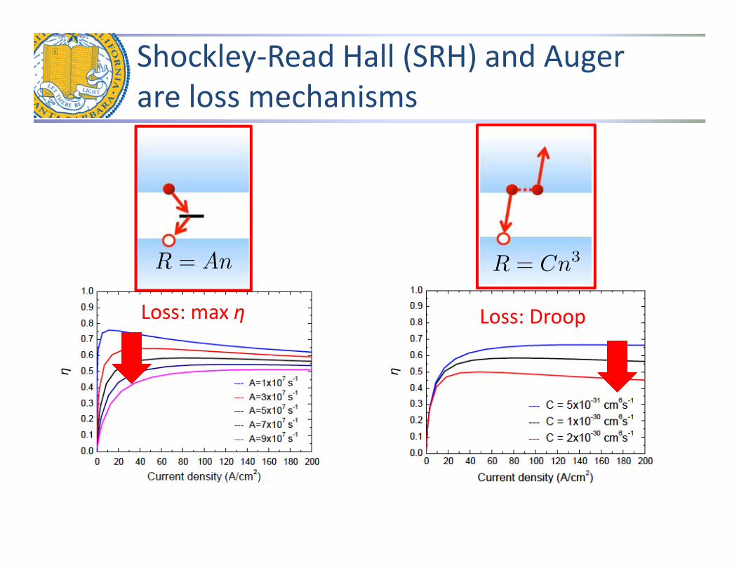
Loss: max η Loss: Droop
Shockley‐Read Hall (SRH) and Auger are loss mechanisms
η η
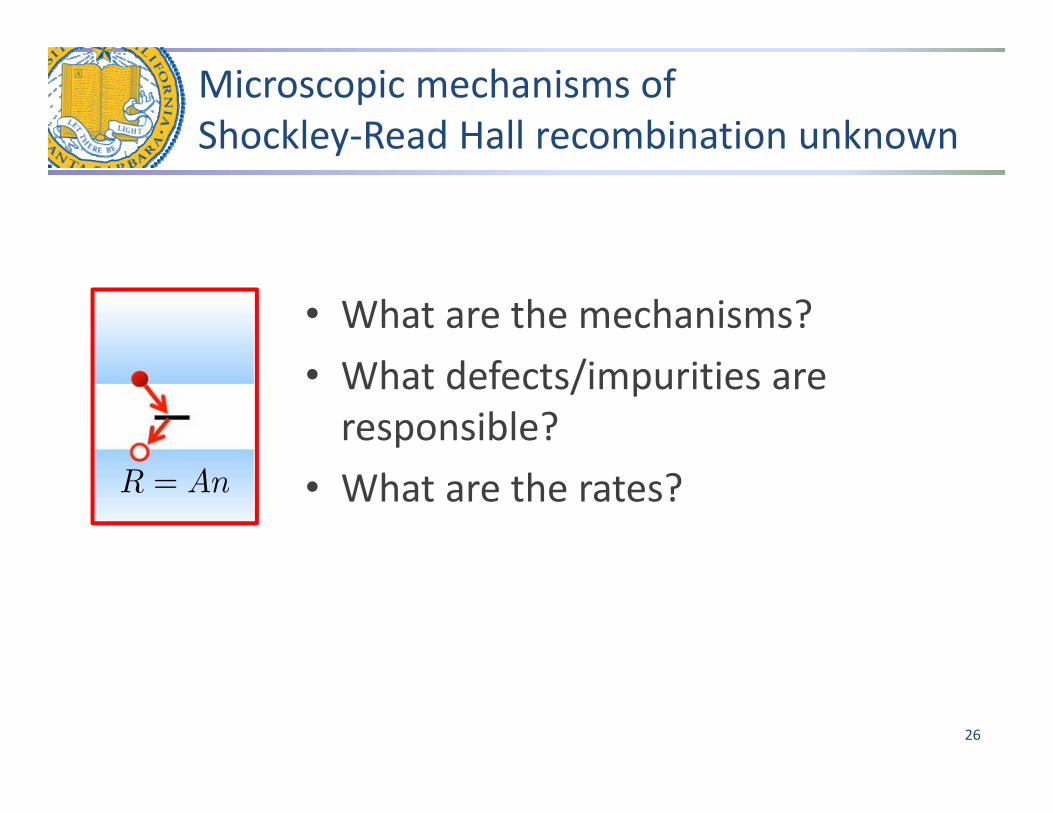
Microscopic mechanisms of Shockley‐Read Hall recombination unknown
26
• What are the mechanisms?• What defects/impurities are responsible?
• What are the rates?
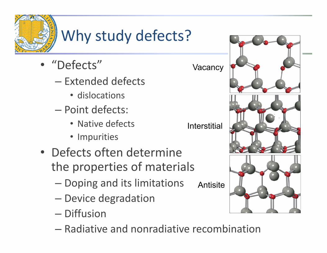
Why study defects?
• “Defects”– Extended defects
• dislocations– Point defects:
• Native defects• Impurities
• Defects often determine the properties of materials– Doping and its limitations– Device degradation– Diffusion – Radiative and nonradiative recombination
Vacancy
Interstitial
Antisite

Formalism
• Eform: formation energy Concentration of defects or impurities:
C = Nsites exp [ Eform/kT]
• Example: gallium vacancy in GaNEform(VGa
3) = Etot(VGa3) Etot(bulk) + Ga 3 EF
O: energy of oxygen in reservoir, i.e., oxygen chemical potentialEF: energy of electron in its reservoir, i.e., the Fermi level
• General expressionEform(Dq) = Etot(Dq) Etot(bulk) + ni i + qEF
ni: number of atoms being exchanged to form the defect
3
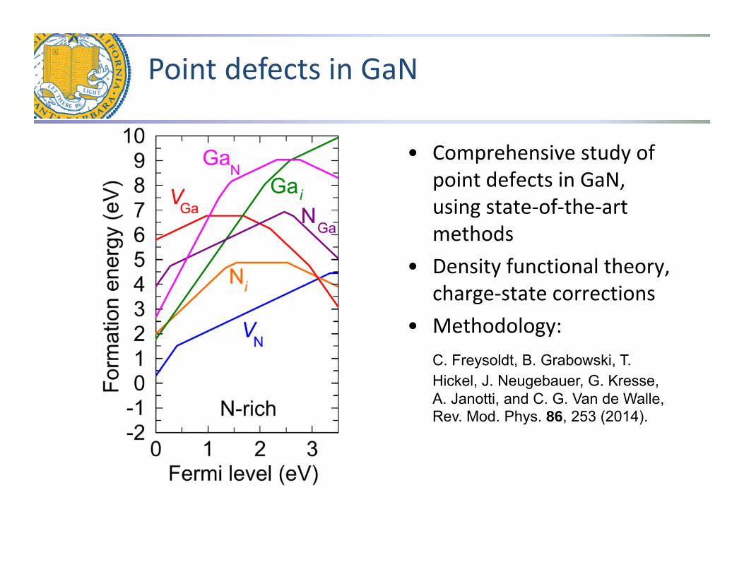
Point defects in GaN
• Comprehensive study of point defects in GaN, using state‐of‐the‐art methods
• Density functional theory, charge‐state corrections
• Methodology: C. Freysoldt, B. Grabowski, T. Hickel, J. Neugebauer, G. Kresse, A. Janotti, and C. G. Van de Walle, Rev. Mod. Phys. 86, 253 (2014).

Impurities in GaN: Carbon
• Carbon: common unintentional impurity
• Carbon on a nitrogen site: defect level ~1 eV above the valence band
J. L. Lyons, A. Janotti, C. G. Van de Walle, Appl. Phys. Lett. 97, 152108 (2010); Phys. Rev. B 89, 035204 (2014)

First‐principles approach for studying loss mechanisms
• Density functional theory (DFT)• Hybrid functional provides
accurate description of – Band gaps– Localized states– Vibronic properties of defects
• Supercell approach for studying defects
31
J. Heyd, G. E. Scuseria, M. Ernzerhof, J. Chem. Phys. 118, 8207 (2003)
J. L. Lyons, A. Janotti, and C. G. Van de Walle, Phys. Rev. B 89, 035204 (2014).

Shockley‐Read Hall (SRH) based on nonradiative capture of carriers by defects
• First step to understand SRH: Calculate rate of nonradiativecapture at defects
• Given by: – Defect density ND, NA
– Carrier density n,p– Capture coefficient Cp, Cn
• Capture coefficient gives rate of capture of one carrier at one defect in a volume V: Cn/p = V r
• Capture due to change in electronic state due to electron‐phonon coupling
32

General form of nonradiativecapture coefficient
Describes transition from initial electronic state (i) and vibronic state (m)
to final electronic state (f) and vibronic state (n)
33
Thermal occupation of phonons
Electron‐phonon coupling
Energy conservation
Volume

First order in the electron‐phonon coupling
Describes transition from initial electronic state (i) and vibronic state (m)
to final electronic state (f) and vibronic state (n)
34
Wif, Electron‐phonon coupling Overlap between vibronic states

Electron‐phonon coupling: One‐dimensional approximation
• Consider one special phonon mode that couples most strongly to distortion caused by carrier capture
• Good approximation for system with strong electron‐phonon coupling– Gives accurate phonon broadening of lineshapes
35
A. Alkauskas et al.,Phys. Rev. Lett. 109, 267401 (2012).
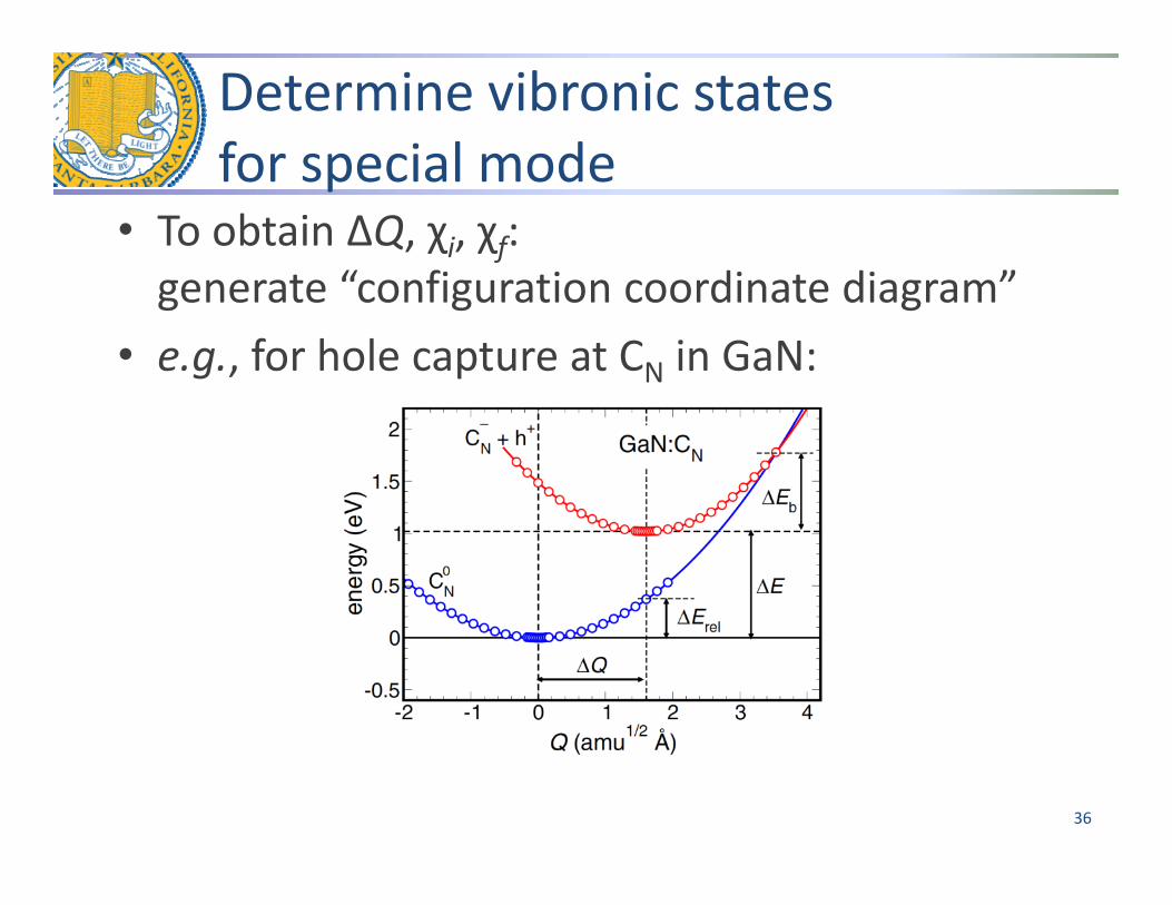
Determine vibronic states for special mode
• To obtain ΔQ, χi, χf: generate “configuration coordinate diagram”
• e.g., for hole capture at CN in GaN:
36

Electron‐phonon coupling for special mode
• DFT calculations yield – single‐particle wavefunctions (ψi/f)– eigenvalues (εi/f) – response to displacement Q
37
Approximate many‐body quantities by single‐particle counterparts
see also: L. Shi and L.‐W. Wang, Phys. Rev. Lett. 109, 245501 (2012).
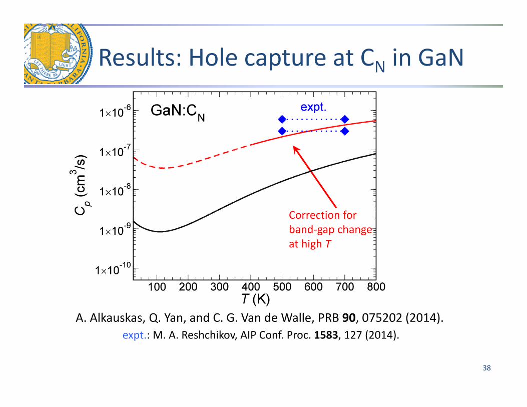
Results: Hole capture at CN in GaN
38
Correction for band‐gap change at high T
expt.: M. A. Reshchikov, AIP Conf. Proc. 1583, 127 (2014).A. Alkauskas, Q. Yan, and C. G. Van de Walle, PRB 90, 075202 (2014).

In progress: Hole capture at VGacomplexes
• Complexes with VGa have midgap levels, may be important as recombination centers
• VGa‐ON‐H: Cp ≅ 8 x 10‐11 cm3s‐1
• VGa‐2H: Cp ≅ 2 x 10‐10 cm3s‐1
39

Summary• First‐principles approach for
nonradiative capture rates
• Luminescence lineshapes for cases of strong and intermediate electron‐phonon coupling
• Origin of SRH recombination in nitrides
40
A. Alkauskas, B. B. Buckley, D. D. Awschalom, and C. G. Van de Walle, New J. Phys. 16, 073026 (2014).
A. Alkauskas, Q. Yan, and C. G. Van de Walle, Phys. Rev. B 90, 075202 (2014).