OPTOELECTRONIC and PHOTOVOLTAIC DEVICES · OPTOELECTRONIC and PHOTOVOLTAIC DEVICES 1. ... III – V...
65
OPTOELECTRONIC and PHOTOVOLTAIC DEVICES 1. Introduction to the (semiconductor) physics: energy bands, charge carriers, semiconductors, p-n junction, materials, etc. 2. Light emitting diodes Light emitting devices 3. Semiconductor lasers (displays, illumination) 4. Photodetectors Light absorbing devices 5. Photovoltaic solar cells (Photodiodes) Outline • Principles of operation (physical background) • Design and structure • Fabrication http://www.lht.ovgu.de/studium/Lehrveranstaltungen.html 1
-
Upload
phungquynh -
Category
Documents
-
view
251 -
download
3
Transcript of OPTOELECTRONIC and PHOTOVOLTAIC DEVICES · OPTOELECTRONIC and PHOTOVOLTAIC DEVICES 1. ... III – V...

OPTOELECTRONIC and PHOTOVOLTAIC
DEVICES
1. Introduction to the (semiconductor) physics: energy bands, charge carriers, semiconductors, p-n
junction, materials, etc.
2. Light emitting diodes Light emitting devices
3. Semiconductor lasers (displays, illumination)
4. Photodetectors Light absorbing devices
5. Photovoltaic solar cells (Photodiodes)
Outline
• Principles of operation (physical background)
• Design and structure
• Fabrication
http://www.lht.ovgu.de/studium/Lehrveranstaltungen.html
1

OPTOELECTRONIC and PHOTOVOLTAIC
DEVICES
[1] B. G. STREETMANN, S. K. BANERJEE: Solid state
electronic devices 6th ed.
[2] S. M. SZE: Physics of semiconductors devices
[3] Ch. KITTEL: Introduction to solid state physics
Technology
[4] J. D. PLUMMER, M. D. DEAL, P. B. GRIFFIN: Silicon VLSI
technology: fundamentals, practice and modeling
[5] S. K. GHANDHI: CLSI fabrication principles: silicon and
gallium arsenide
[6] S. A. CAMPBELL: The science and engineering of
microelectronic fabrication
[7] P.MOTTIER: LEDs for lighting applications
Literature recommendation
http://www.lht.ovgu.de/studium/Lehrveranstaltungen.html
2

1. Introduction
charge transport in solids depends not only on the properties
of the electron but also on the arrangement of atoms.
SEMICONDUCTORS:
electric conductivities intermediate between metals and
insulators
conductivity can be varied over orders of magnitude by
changes in temperature
optical excitation
impurity content
1.1. Overview of Semiconductors
3
1. Introduction
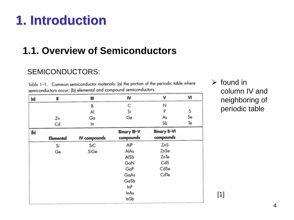
SEMICONDUCTORS:
found in
column IV and
neighboring of
periodic table
1.1. Overview of Semiconductors
[1]
4
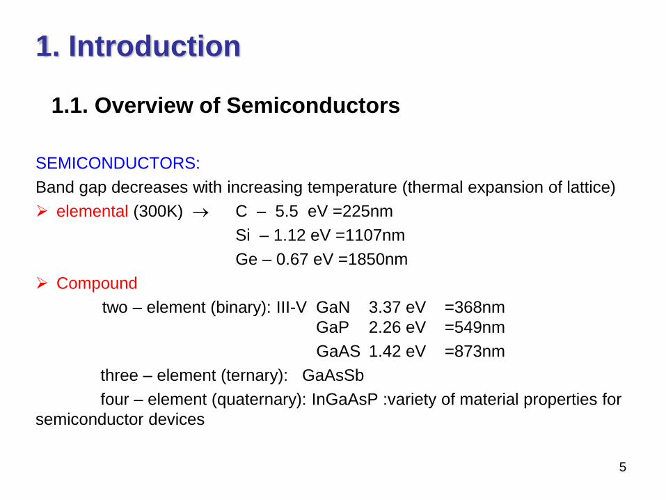
1. Introduction
SEMICONDUCTORS:
Band gap decreases with increasing temperature (thermal expansion of lattice)
elemental (300K) C – 5.5 eV =225nm
Si – 1.12 eV =1107nm
Ge – 0.67 eV =1850nm
Compound
two – element (binary): III-V GaN 3.37 eV =368nm
GaP 2.26 eV =549nm
GaAS 1.42 eV =873nm
three – element (ternary): GaAsSb
four – element (quaternary): InGaAsP :variety of material properties for
semiconductor devices
1.1. Overview of Semiconductors
5

1. Introduction
SEMICONDUCTORS:
Binary, ternary, quaternary:
:variety of material properties
for semiconductors devices
1.1. Overview of Semiconductors
[1]
6

1. Introduction
SEMICONDUCTORS:
Compound
II-VI: Fluorescent materials: ZnS (phosphors)
Light detectors: CdSe
InSb (III – V)
most important characteristic of semiconductors band gap
1.1. Overview of Semiconductors
7

1. Introduction
ATOMS electrons restricted to sets of discrete energy levels
QUANTUM MECHANICS
SOLIDS same expected, will see: discrete energy levels spread into
BANDS
wave functions of electrons overlap, electrons are not localized
1.2. Bonding forces
8
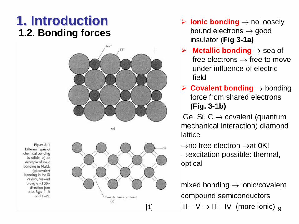
1. Introduction Ionic bonding no loosely
bound electrons good
insulator (Fig 3-1a)
Metallic bonding sea of
free electrons free to move
under influence of electric
field
Covalent bonding bonding
force from shared electrons
(Fig. 3-1b)
Ge, Si, C covalent (quantum
mechanical interaction) diamond
lattice
no free electron at 0K!
excitation possible: thermal,
optical
mixed bonding ionic/covalent
compound semiconductors
III – V II – IV (more ionic)
1.2. Bonding forces
[1] 9

1. Introduction
Atoms brought together interactions
Result: balance of attraction and repulsion
Lattice spacing (equilibrium)
Electron energy level configuration
Result of PAULI exclusion principle:
no atomic interaction: identical electronic structures
spacing smaller: overlapping of wave functions
no two electrons of the system may have the same quantum state
splitting of discrete levels
bands
1.3. Energy bands
10

1. Introduction EXAMPLE: two atoms
interacting: Quantum mechanics
(solving Schrödinger equation)
composite two – electron wave
functions are linear combinations
of the individual atomic orbitals
LCAO (Fig. 3-2)
bonding orbital/antibonding
orbital higher value of wave
function higher e- probability
density between atoms
bonding energy level lower than
antibonding (and single level
before)
cohesion of crystal
MANY ATOMS: number of
energy levels depend on number
of atoms
lowest level: totally symmetric
LCAO
highest level: totally
antisymmetric LCAO
1.3. Energy bands
[1]
11

1. Introduction 1.3. Energy bands
EXAMPLE
Imaginary formation of Si
crystal (Fig. 3-3)
Si atom structure
bands grow (smaller
distance)
bands split
repulsive forces
conduction band
energy gap (forbidden
band)
valence band
Characteristic for
semiconductors
[1]
12

1. Introduction 1.4. Metals, semiconductors, and insulators
Completely filled band (at 0 K): no net charge transport possible (Fig. 3-4)
even when electric field applied
Metal: band overlap and/or partly filled bands
Semiconductor: gap < 5 eV (diamond)
Insulator: gap > 5eV
[1]
Room temp.
kT=0.026 eV (mean thermal
energy free of particle
at 300K)
13

1. Introduction
Conservation principle: for energy and momentum
Quantitative calculations can be made of band structures:
typical calculation: single electron travels trough perfectly periodic lattice
wave function of electron: plane wave
space dependent wave function (x-direction)
𝜓𝑘 𝑥 = 𝑈 𝑘𝑥, 𝑥 𝑒𝑖𝑘𝑥 𝑥
𝑘𝑥 =1
ℏ𝑝
𝑥 propagation constant (wave vector)
𝑈 𝑘𝑥, 𝑥 modulates the wave function according to the periodicity of
lattice (potential)
1.5. Direct and indirect semiconductors
Physical meaning: (absolute value)2
probability density
integral: prob. to
find electron at
location
14

1. Introduction
Allowed values of energy can be plotted vs 𝑘
1.5. Direct and indirect semiconductors
[1]
15

1. Introduction 1.5. Direct and indirect semiconductors
Periodicity different in
various directions.
(E, 𝑘)diagram plotted for
various directions:
complex surface in 3d
[1] 16
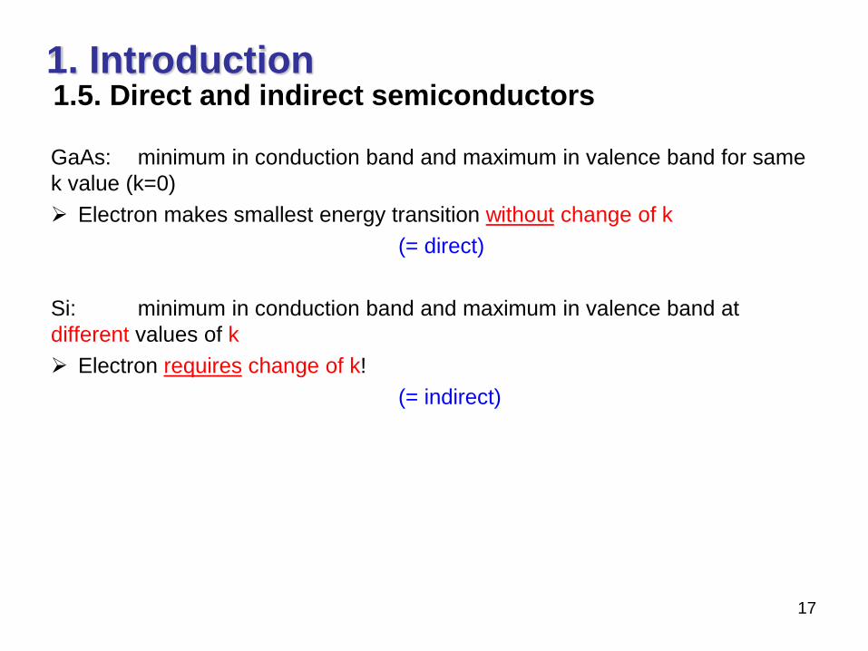
1. Introduction
GaAs: minimum in conduction band and maximum in valence band for same
k value (k=0)
Electron makes smallest energy transition without change of k
(= direct)
Si: minimum in conduction band and maximum in valence band at
different values of k
Electron requires change of k!
(= indirect)
1.5. Direct and indirect semiconductors
17
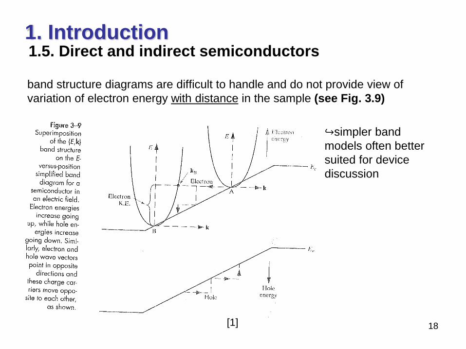
1. Introduction
band structure diagrams are difficult to handle and do not provide view of
variation of electron energy with distance in the sample (see Fig. 3.9)
simpler band
models often better
suited for device
discussion
1.5. Direct and indirect semiconductors
[1] 18

1. Introduction
Electron – momentum in the crystal connected to k:
𝑝𝑥 = ℏ𝑘𝑥 (ℏ =ℎ
2𝜋)
GaAs: electron from conduction band can fall into empty state in valence
band
giving of energy difference Eg as a photon of light
Si: change of energy and momentum
for example: electron energy goes through defect states within band gap
energy is given up as heat to lattice (phonon) rather than as emitted photon
optical devices:
made of materials capable of direct band – to – band transitions
OR
indirect materials with vertical transitions between defect states
1.5. Direct and indirect semiconductors
19
1. Introduction
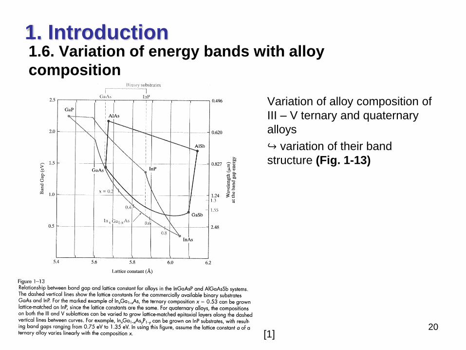
Variation of alloy composition of
III – V ternary and quaternary
alloys
variation of their band
structure (Fig. 1-13)
1.6. Variation of energy bands with alloy
composition
[1] 20
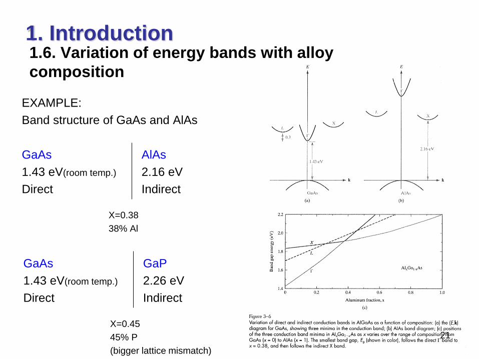
1. Introduction
EXAMPLE:
Band structure of GaAs and AlAs
1.6. Variation of energy bands with alloy
composition
GaAs
1.43 eV(room temp.)
Direct
AlAs
2.16 eV
Indirect
X=0.38
38% Al
GaAs
1.43 eV(room temp.)
Direct
GaP
2.26 eV
Indirect
X=0.45
45% P
(bigger lattice mismatch)
21

1. Introduction
! Light emission most efficient in direct semiconductors!
GaAs1-xPx best for X< 0,45 (RED LED´s: x = 0,4)
Eg 1,9 eV
650nm
(conversion between energy E of a photon of light in eV and its wavelength)
λ in nm : λ = 1240𝑛𝑚⋅𝑒𝑉
𝐸)
1.6. Variation of energy bands with alloy
composition
22

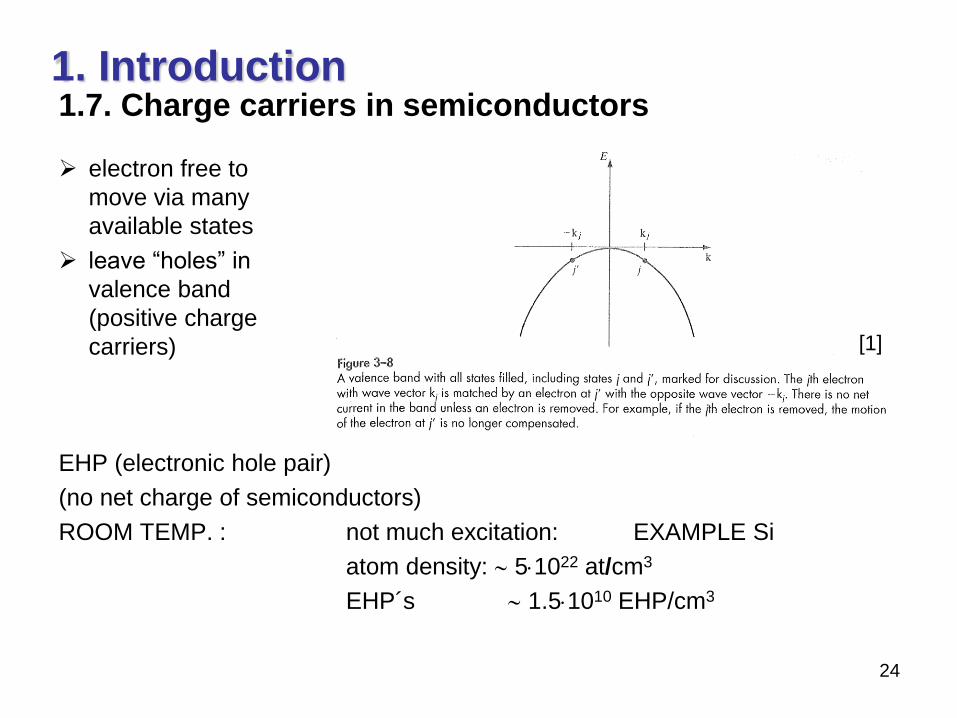
1. Introduction
0 K and band gap valence band: completely filled
conduction band: empty
no free carriers insulator
EXCITATION by temperature: 𝑛 ~ 𝑒−𝐸𝑔
2𝑘𝑇 Room T : kT=0.0259eV
Temperature raised some electrons receive enough energy to be excited
across the band gap
1.7. Charge carriers in semiconductors
electron free to
move via many
available states
leave “holes” in
valence band
(positive charge
carriers) Electron-hole pair
(EHP)
[1] 23
1. Introduction
EHP (electronic hole pair)
(no net charge of semiconductors)
ROOM TEMP. : not much excitation: EXAMPLE Si
atom density: 51022 at/cm3
EHP´s 1.51010 EHP/cm3
1.7. Charge carriers in semiconductors
electron free to
move via many
available states
leave “holes” in
valence band
(positive charge
carriers)
[1]
24

1. Introduction
INTRINSIC MATERIAL n=p=ni (electron/hole concentration [1/cm³])
Equilibrium: generation of EHP´s = recombination ri =gi
at any temperature the rate of recombination of electrons and holes (ri)
is proportional to equilibrium concentration n0,p0
ri = rn0p0=rni2=gi
r constant of proportionality for recombination
1.7. Charge carriers in semiconductors
[1] 25

1. Introduction
INTRINSIC MATERIAL
n=p=ni
1.7. Charge carriers in semiconductors
26 [1]
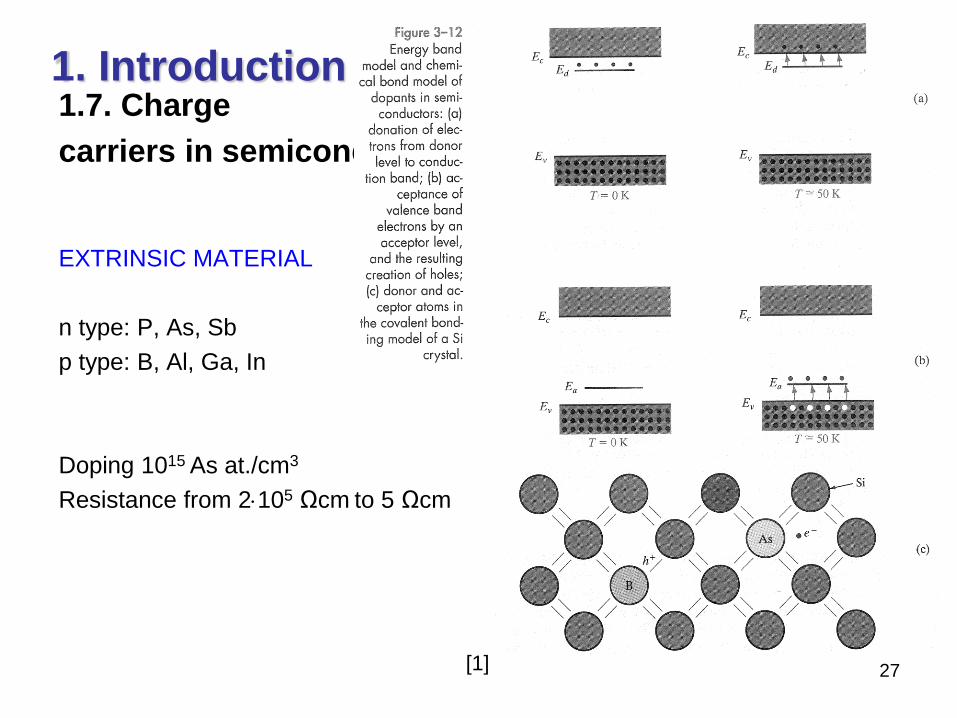
1. Introduction 1.7. Charge
carriers in semiconductors
EXTRINSIC MATERIAL
n type: P, As, Sb
p type: B, Al, Ga, In
Doping 1015 As at./cm3
Resistance from 2105 Ωcm to 5 Ωcm
[1] 27

1. Introduction 1.7. Charge
carriers in semiconductors
EXTRINSIC MATERIAL
Doping 1015 As at./cm3 Resistance from 2105 Ωcm to 5 Ωcm
[1] 28

1. Introduction 1.7. Charge carriers in semiconductors
FERMI – LEVEL: electrons in solid obey Fermi – Dirac statistics: • indistinguishability of electrons
• wave nature of electrons
• Pauli exclusion principle
distribution of electrons over a range of allowed energy levels at thermal
equilibrium:
f(𝐸) =1
1+ 𝑒(𝐸−𝐸𝐹)/𝑘𝑇
k : Boltzmann´s constant (8.6210-5 eV/K)
EF: Fermi level
Fermi – Dirac distribution function =
probability that an available energy state
E will be occupied by an electron at
temperature T
[1] 29

1. Introduction 1.7. Charge carriers in semiconductors
30 [1]
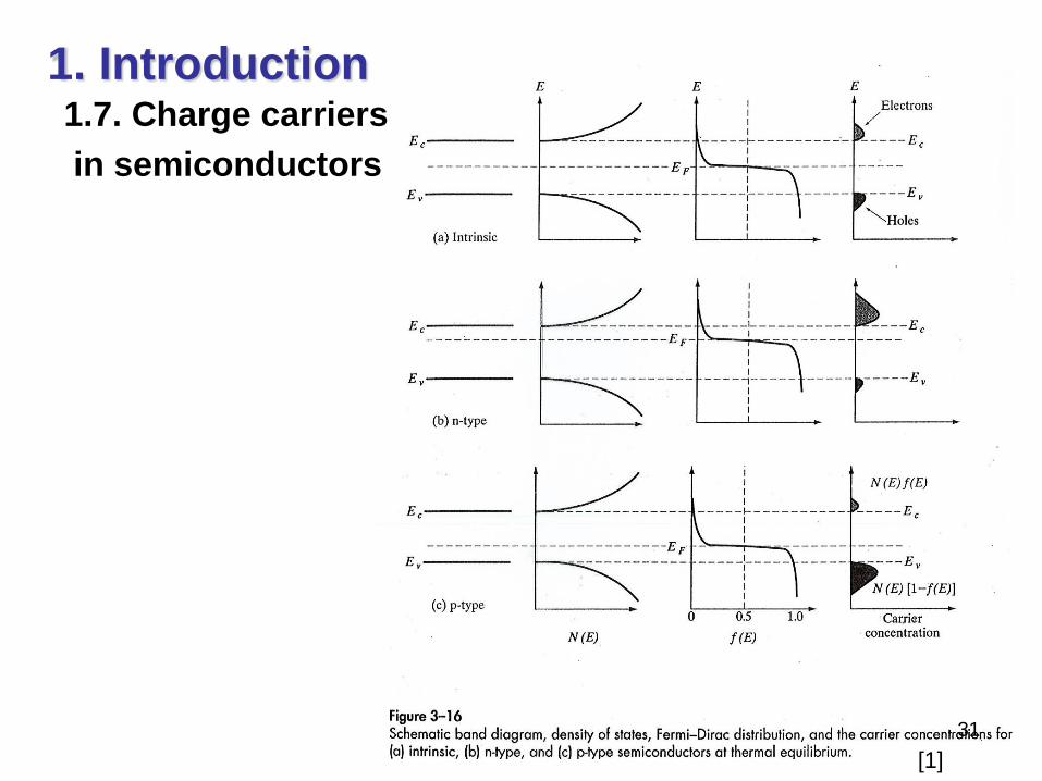
1. Introduction 1.7. Charge carriers
in semiconductors
[1]
31

1. Introduction
Usually single – valued (discrete) energy levels from doping and (quasi)
continuum of allowed states in valence and conduction bands
Discrete levels also possible by confinement in quantum wells:
growth of multilayer compound semiconductors by MBE (Molec. Beam Epitaxy) or
MOVPE (Metal Organic Vap. Phase Epitaxy)
adjacent layers with different band gaps (Fig. 3.13)
HETEROJUNCTIONS
1.8. Electrons and holes in quantum wells
32
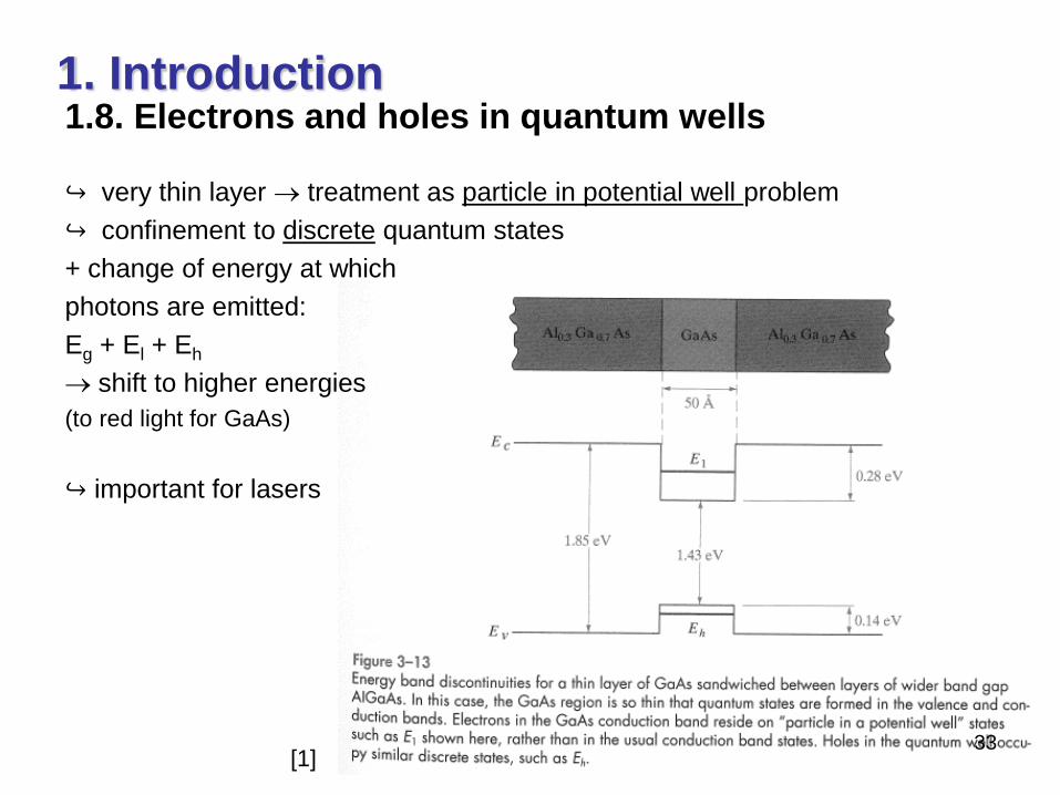
1. Introduction 1.8. Electrons and holes in quantum wells
very thin layer treatment as particle in potential well problem
confinement to discrete quantum states
+ change of energy at which
photons are emitted:
Eg + El + Eh
shift to higher energies
(to red light for GaAs)
important for lasers
[1] 33
1. Introduction 1.8. Excess carriers in semiconductors
creation of charge carriers in excess of thermal equilibrium values
optical excitation
electron bombardment
carrier injection (forward – biased pn – junction)
Excess carriers can dominate the conduction of the semiconductor
34
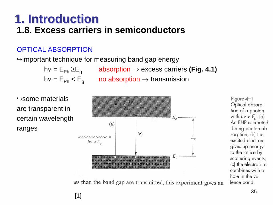
1. Introduction 1.8. Excess carriers in semiconductors
OPTICAL ABSORPTION
important technique for measuring band gap energy
h = EPh Eg absorption excess carriers (Fig. 4.1)
h = EPh < Eg no absorption transmission
some materials
are transparent in
certain wavelength
ranges
[1] 35
1. Introduction 1.8. Excess carriers in semiconductors
OPTICAL ABSORPTION
possible to “see through” certain insulators: NaCl, SiO2 (crystalline)
Eg 2eV infrared and red part of visible spectrum transmitted
Eg 3eV infrared and all visible light transmitted
Ratio of transmitted to incident light intensity depend on wavelength,
(material), and thickness of the sample
[1] 36

1. Introduction 1.8. Excess carriers in semiconductors
OPTICAL ABSORPTION
probability of absorption in any dx is constant
decrease of intensity - 𝑑𝐼(𝑥)
𝑑𝑥 is proportional to remaining intensity at x
- 𝑑𝐼 𝑥
𝑑𝑥= 𝐼 𝑥
37 [1]
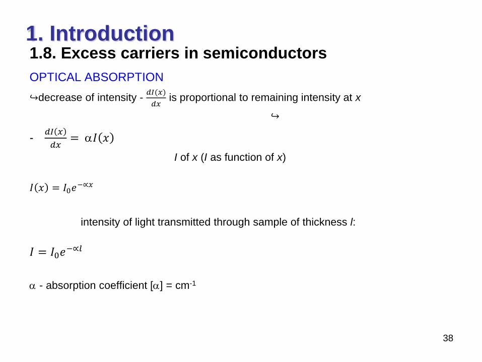
1. Introduction 1.8. Excess carriers in semiconductors
OPTICAL ABSORPTION
decrease of intensity - 𝑑𝐼(𝑥)
𝑑𝑥 is proportional to remaining intensity at x
-𝑑𝐼 𝑥
𝑑𝑥= 𝐼 𝑥
I of x (I as function of x)
𝐼 𝑥 = 𝐼0𝑒
−∝𝑥
intensity of light transmitted through sample of thickness l:
𝐼 = 𝐼0𝑒−∝𝑙
- absorption coefficient [] = cm-1
38

1. Introduction 1.8. Excess carriers in semiconductors
OPTICAL ABSORPTION
absorption edge
39 [1]
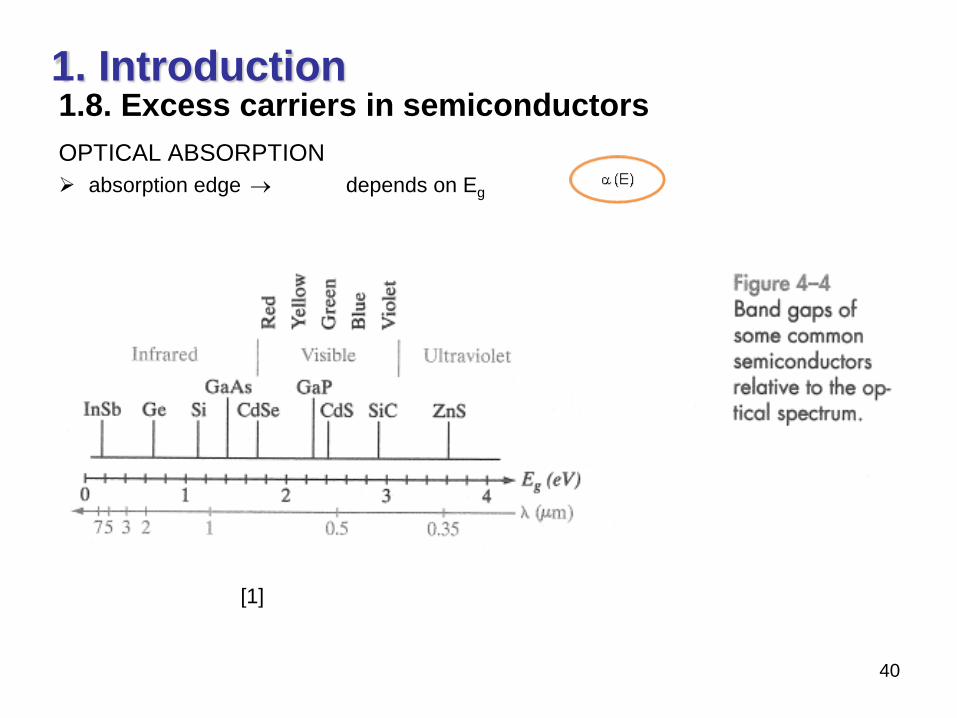
1. Introduction 1.8. Excess carriers in semiconductors
OPTICAL ABSORPTION
absorption edge depends on Eg
40
[1]
1. Introduction 1.9. Luminescence
recombination of EHPs or carriers excited into higher energy levels fall to
equilibrium states:
light can be given off the material
best for direct semiconductor
property of light emission luminescence
Depending on excitation mechanism:
photoluminescence: photon absorption
cathodoluminescence: high – energy electron bombardment
electroluminescence: introduction of current into sample
(most important)
different to incandescence! hot process (heated materials)
Luminescence
cold process (here: colder is better)
41
1. Introduction 1.9. Photoluminescence
Simplest example of light emission from Semiconductors:
direct excitation and recombination of EHPs by photon
Steady state excitation: same rate of generation and recombination
FLUORESCENCE
direct recombination FAST: mean lifetime of EHP 10-8 s or less.
emission stops within 10-8s after excitation turned off
PHOSPHORESCENCE
slow processes sec to minutes after excitation removed
(Materials =phosphors) ZnS
defect level with tendency to temporarily capture (trap) electron from
conduction band
42
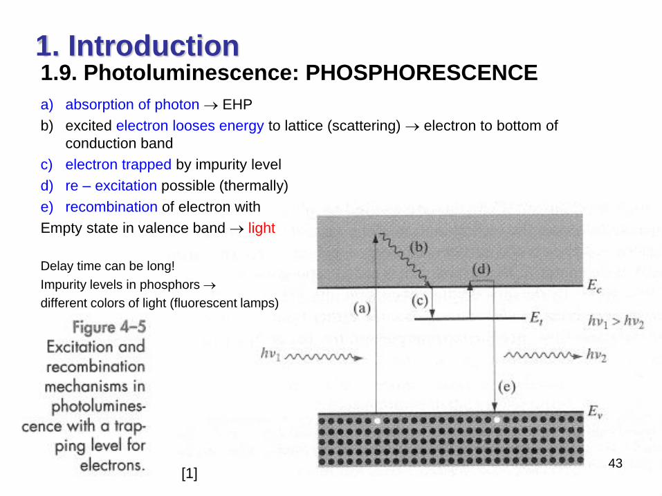
1. Introduction 1.9. Photoluminescence: PHOSPHORESCENCE
a) absorption of photon EHP
b) excited electron looses energy to lattice (scattering) electron to bottom of
conduction band
c) electron trapped by impurity level
d) re – excitation possible (thermally)
e) recombination of electron with
Empty state in valence band light
Delay time can be long!
Impurity levels in phosphors
different colors of light (fluorescent lamps)
43 [1]

1. Introduction 1.9. Electroluminescence
ELECTROLUMINESCENCE
electrical energy to generate photon emission in solid
LED: electrical current causes injection of MINORITY CARRIERS into
regions where they recombine (with majority carriers)
recombination radiation
= injection electroluminescence
First electroluminescent effect observed:
emission of photons by certain phosphors in alternating electric field
ZnS in a binder materials (plastic, high – k)
44

1. Introduction 1.10. Electron transition
45 [2]
1) Interband transitions: a) intrinsic emission, b) higher – energy emission (hot carriers)
2) Transition involving impurity or defects: a) CB to acceptor type defect, b) donor –
type defect to VB, c) donor to acceptor emission (pair emission), d) band – to band
emission via deep
level traps
3) intraband
transition involving
hot carriers
(longer process)
not all radiative, not
all can occur in same
material under same
conditions

1. Introduction 1.10. Interaction between photon and electron
46
Three main optical process for interaction between photon and electron in solids:
1. Absorption of photon by excitation
of electrons from filled state in VB to
empty states in CB
PHOTODETECTOR/SOLAR CELL
2. Electron of CB can spontaneously
return to empty state in VB
(recombination with emission of photon)
LED
3. Incoming photon can stimulate
emission of similar photon by
recombination free photons
coherent LASER
[2]

1. Introduction 1.11. Carrier lifetime
47
excess carriers increase in conductivity
photoconductivity ()
𝐽 = 𝐸 = 𝑞(𝑛µ𝑛 + 𝑝µ𝑒)𝐸
= 𝑞(𝑛µ𝑛 + 𝑝µ𝑝) ,
(µ𝑛 = − <𝑣𝑥>
𝐸𝑥)
1. Introduction 1.11. Carrier lifetime
48
Mechanisms of recombination and recombination kinetics:
Direct recombination of electrons and holes
Indirect recombination
Direct recombination:
Excess electrons and holes decay by electrons falling from conduction band
to empty states (holes) in valence band
energy loss of electrons photon
• spontaneously: probability of recombination constant in time
Rate of decay of electrons at any time t is proportional to number of electrons remaining
at t and number of holes, with some constant of proportionality for recombination (𝑟).

1. Introduction 1.11. Carrier lifetime: direct recombination
49
Net rate of change in conduction band electron concentration:
Thermal generation rate – recombination rate
𝑑𝑛(𝑡)
𝑑𝑡= 𝑟𝑛𝑖
2 − 𝑟𝑛 𝑡 𝑝(𝑡)
(thermal generation =recombination, intrinsic material)
ASSUMPTION:
excess e- - h+ – population created at t = 0 (short flash of light)
initial excess e- and h+ concentration equal n = p
• e- and h+ recombine in pairs instantaneous concentrations of excess carriers also
equal • n(t) = p(t)
𝑑𝑛 𝑡
𝑑𝑡= 𝑟𝑛𝑖
2 − 𝑟 𝑛0 + 𝑛 𝑡 𝑝0 + 𝑝 𝑡
: initial
: instantaneous
Degradation of
excess carriers
equilibrium value excess value

1. Introduction 1.11. Carrier lifetime: direct recombination
50
𝑑𝑛 𝑡
𝑑𝑡= 𝑟𝑛𝑖
2 − 𝑟 𝑛0 + 𝑛 𝑡 𝑝0 + 𝑝 𝑡
(𝑛 = 𝑝) and 𝑛0𝑝0 = 𝑛𝑖2
𝑑𝑛 𝑡
𝑑𝑡= 𝑟𝑛𝑖
2 − 𝑟 𝑛0 + 𝑛 𝑡 𝑝0 + 𝑝 𝑡 = −𝑟 (𝑛0+𝑝0 𝑛 𝑡 + 𝑛2 𝑡 ]
: excess
0: equilibrium
Degradation of
excess carriers equilibrium value excess value

1. Introduction 1.11. Carrier lifetime: direct recombination
51
𝑑𝑛 𝑡
𝑑𝑡= −𝑟 (𝑛0+𝑝0 𝑛 𝑡 + 𝑛2 𝑡 ]
Difficult to solve
simplification: excess carrier concentration small n2 to neglect
material is extrinsic neglect the term for minority carriers
example: p – type (p0 >> n0)
𝑑𝑛(𝑡)
𝑑𝑡 = - r𝑝0n(t)
n(t) = ∆n 𝑒−𝑟𝑝0𝑡 = ∆n 𝑒−𝑡/𝑛
𝑛 - recombination lifetime (= (𝑟𝑝0)
−1)
(minority carrier lifetime)
𝑝=(𝑟𝑛0)
−1) for excess holes in n – type
: excess
0: equilibrium

1. Introduction 1.11. Carrier lifetime: direct recombination
52
Approximation: extrinsic material
low – level injection n(t) n(t)
p(t) p0
more general expression for carrier lifetime
𝑛 = 1
𝑟(𝑛𝑜 + 𝑝0)
valid for n – or p – type if injection level is low

1. Introduction 1.11. Carrier lifetime: direct recombination
53
for direct recombination:
excess majority carriers
decay at same rate as
minority carriers
however: large percentage
change for minority carrier
concentration
small percentage
change for majority carrier
concentration
[1]
1. Introduction 1.11. Carrier lifetime: indirect recombination
54
Indirect recombination: trapping
column IV semiconductors and certain compounds
probability of direct recombination is small
majority of recombination in indirect material
via recombination levels within band gap
energy loss of electron given up to lattice as heat rather than photons
Any impurity or lattice defect can serve as recombination center if it is capable of:
1. receive carrier of one type
2. capture opposite type of carrier(subsequently)
annihilation of pair

1. Introduction 1.11. Carrier lifetime: indirect recombination
55
Example: recombination level Er (below EF) filled with electrons (Fig. 4-8).
1. hole capture by Er (electron of Er to hole in VB heat)
2. electron capture by Er (electron of CB to Er heat)
[1]

1. Introduction 1.11. Carrier lifetime: indirect recombination
56
Carrier lifetime from indirect recombination more complicated
• unequal times for capturing each type of carriers
recombination often delayed, captured carrier can be thermally reexcited
before capture of opposite carrier can occur
temporary trapping
Types of impurity or defect centers
1. trapping center (trap): after capture of one type of carrier, most probable next event
is reexcitation
2. recombination center: after capture of one type of carrier, most probable next event
is capture of opposite type of carrier

1. Introduction 1.11. Carrier lifetime: indirect recombination
57
Trapping and recombination centers. (deep levels mostly slower)
1. Introduction 1.11. Carrier lifetime: indirect recombination
58
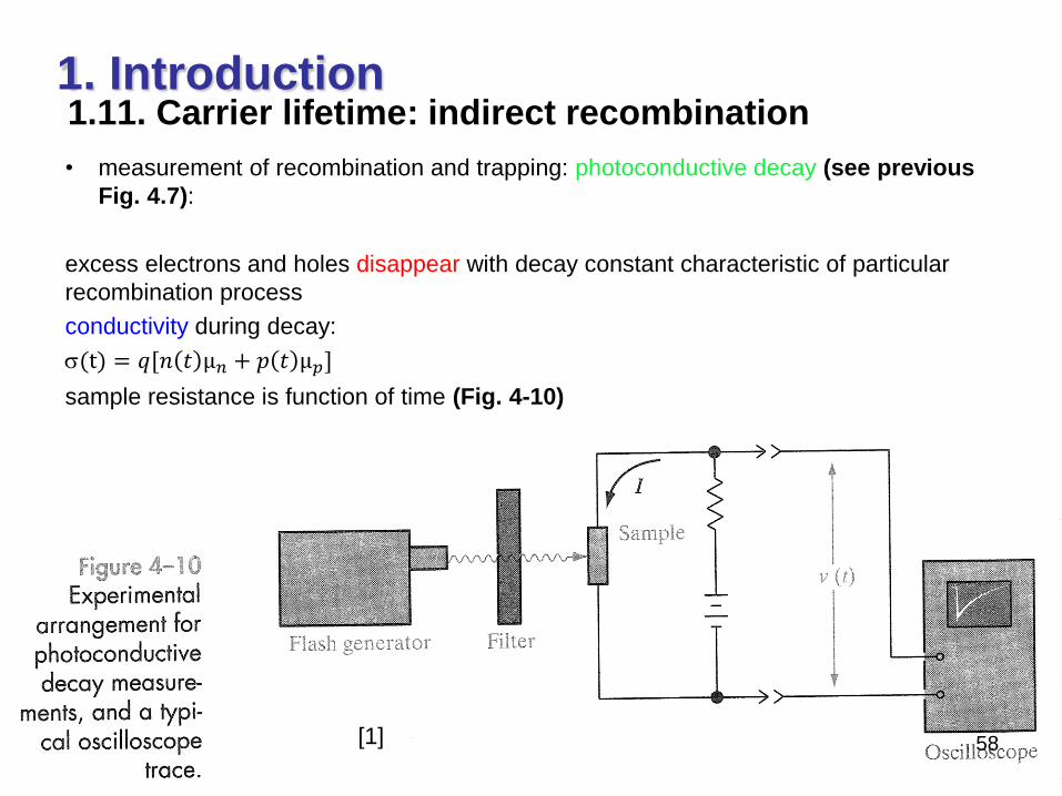
• measurement of recombination and trapping: photoconductive decay (see previous
Fig. 4.7):
excess electrons and holes disappear with decay constant characteristic of particular
recombination process
conductivity during decay:
(t) = 𝑞[𝑛 𝑡 µ𝑛 + 𝑝 𝑡 µ𝑝]
sample resistance is function of time (Fig. 4-10)
[1]

1. Introduction 1.12. Steady state carrier generation
59
Recombination also important in samples at thermal equilibrium or steady state EHP
generation – recombination balance
• equilibrium: no external excitation, no net motion of charge (constant T, sample
in the dark, no fields applied)
• steady state: non equilibrium condition in which all processes are constant and
balanced by opposing processes (constant current or constant optical generation
of EHP´s)
• in equilibrium: thermal generation of EHP`s at rate
g(T) = gi
balanced by recombination so that equilibrium concentrations n0 and p0 maintained:
g(T) =rni2 = rn0p0
can include generation
from defect centers as
well as band – band
generation
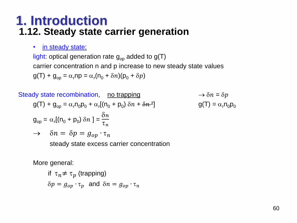
1. Introduction 1.12. Steady state carrier generation
60
• in steady state:
light: optical generation rate gop added to g(T)
carrier concentration n and p increase to new steady state values
g(T) + gop = rnp = r(n0 + 𝑛)(p0 + 𝑝)
Steady state recombination, no trapping 𝑛 = 𝑝
g(T) + gop = rn0p0 + r[(n0 + p0) 𝑛 + 𝑛 ²] g(T) = rn0p0
gop = r[(n0 + p0) 𝑛 ] = 𝑛
𝑛
𝑛 = 𝑝 = 𝑔𝑜𝑝 ∙ 𝑛
steady state excess carrier concentration
More general:
if 𝑛≠ 𝑝 (trapping)
𝑝 = 𝑔𝑜𝑝 ∙ 𝑝 and 𝑛 = 𝑔𝑜𝑝 ∙ 𝑛
1. Introduction 1.12. Steady state carrier generation
61
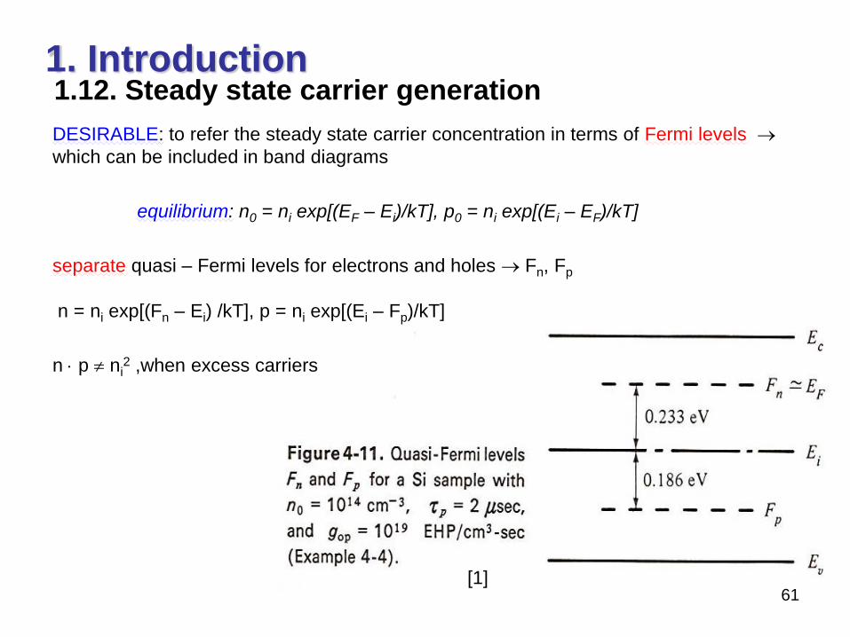
DESIRABLE: to refer the steady state carrier concentration in terms of Fermi levels
which can be included in band diagrams
equilibrium: n0 = ni exp[(EF – Ei)/kT], p0 = ni exp[(Ei – EF)/kT]
separate quasi – Fermi levels for electrons and holes Fn, Fp
n = ni exp[(Fn – Ei) /kT], p = ni exp[(Ei – Fp)/kT]
n p ni2 ,when excess carriers
[1]

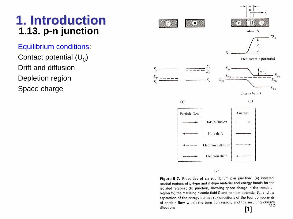
1. Introduction 1.13. p-n junction
62
Equilibrium conditions:
Contact potential (U0)
Drift and diffusion
Depletion region
Space charge
1. Introduction 1.13. p-n junction
63
Equilibrium conditions:
Contact potential (U0)
Drift and diffusion
Depletion region
Space charge
[1]

1. Introduction 1.13. p-n junction
64
Bias at p-n
[1]

1. Introduction 1.13. p-n junction
65
I-V:
[1]