
Opto Electrical Pcb
3
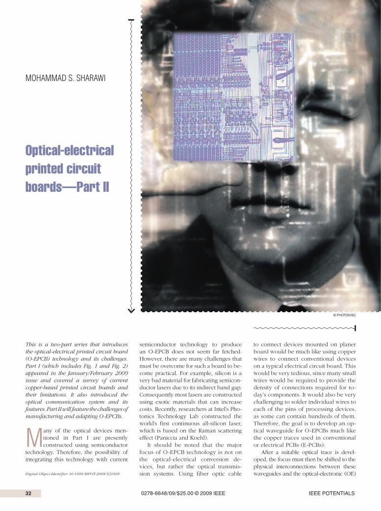
32 IEEE POTENTIALS 0278-6648/09/$25.00 © 2009 IEEE This is a two-part series that introduces the optical-electrical printed circuit board (O-EPCB) technology and its challenges. Part I (which includes Fig. 1 and Fig. 2) appeared in the January/February 2009 issue and covered a survey of current copper-based printed circuit boards and their limitations. It also introduced the optical communication system and its features. Part II will feature the challenges of manufacturing and adapting O-EPCBs. M any of the optical devices men- tioned in Part I are presently constructed using semiconductor technology. Therefore, the possibility of integrating this technology with current semiconductor technology to produce an O-EPCB does not seem far fetched. However, there are many challenges that must be overcome for such a board to be- come practical. For example, silicon is a very bad material for fabricating semicon- ductor lasers due to its indirect band gap. Consequently most lasers are constructed using exotic materials that can increase costs. Recently, researchers at Intel’s Pho- tonics Technology Lab constructed the world’s first continuous all-silicon laser, which is based on the Raman scattering effect (Paniccia and Koehl). It should be noted that the major focus of O-EPCB technology is not on the optical-electrical conversion de- vices, but rather the optical transmis- sion systems. Using fiber optic cable to connect devices mounted on planer board would be much like using copper wires to connect conventional devices on a typical electrical circuit board. This would be very tedious, since many small wires would be required to provide the density of connections required for to- day’s components. It would also be very challenging to solder individual wires to each of the pins of processing devices, as some can contain hundreds of them. Therefore, the goal is to develop an op- tical waveguide for O-EPCBs much like the copper traces used in conventional or electrical PCBs (E-PCBs). After a suitable optical trace is devel- oped, the focus must then be shifted to the physical interconnections between these waveguides and the optical-electronic (OE) Digital Object Identifier 10.1109/MPOT.2008.931499 Optical-electrical printed circuit boards—Part II © PHOTODISC MOHAMMAD S. SHARAWI
-
Upload
satishkumar123 -
Category
Documents
-
view
44 -
download
3
Transcript of Opto Electrical Pcb
32 IEEE POTENTIALS 0278-6648/09/$25.00 © 2009 IEEE
This is a two-part series that introduces the optical-electrical printed circuit board (O-EPCB) technology and its challenges. Part I (which includes Fig. 1 and Fig. 2) appeared in the January/February 2009 issue and covered a survey of current copper-based printed circuit boards and their limitations. It also introduced the optical communication system and its features. Part II will feature the challenges of manufacturing and adapting O-EPCBs.
Many of the optical devices men-tioned in Part I are presently constructed using semiconductor
technology. Therefore, the possibility of integrating this technology with current
semiconductor technology to produce an O-EPCB does not seem far fetched. However, there are many challenges that must be overcome for such a board to be-come practical. For example, silicon is a very bad material for fabricating semicon-ductor lasers due to its indirect band gap. Consequently most lasers are constructed using exotic materials that can increase costs. Recently, researchers at Intel’s Pho-tonics Technology Lab constructed the world’s first continuous all-silicon laser, which is based on the Raman scattering effect (Paniccia and Koehl).
It should be noted that the major focus of O-EPCB technology is not on the optical-electrical conversion de-vices, but rather the optical transmis-sion systems. Using fiber optic cable
to connect devices mounted on planer board would be much like using copper wires to connect conventional devices on a typical electrical circuit board. This would be very tedious, since many small wires would be required to provide the density of connections required for to-day’s components. It would also be very challenging to solder individual wires to each of the pins of processing devices, as some can contain hundreds of them. Therefore, the goal is to develop an op-tical waveguide for O-EPCBs much like the copper traces used in conventional or electrical PCBs (E-PCBs).
After a suitable optical trace is devel-oped, the focus must then be shifted to the physical interconnections between these waveguides and the optical-electronic (OE) Digital Object Identifier 10.1109/MPOT.2008.931499
Optical-electrical printed circuit boards— Part II
© PHOTODISC
MOHAMMAD S. SHARAWI
MARCH/APRIL 2009 33
converters. This would be much like the optical equivalent to the invention of sur-face mounting technology that has allowed the density of connections on E-PCBs to drastically increase, while lowering the cost of production.
A conventional fiber optical com-munication system is much like an elec-tronic circuit constructed using crude connections and bell wire. In order to construct an optical circuit that could be used to interconnect components such as microprocessors, a standardized method must be implemented that will allow dense arrays of optical links at precise locations, much like copper trac-es. This requires the production of very small light pathways or waveguides.
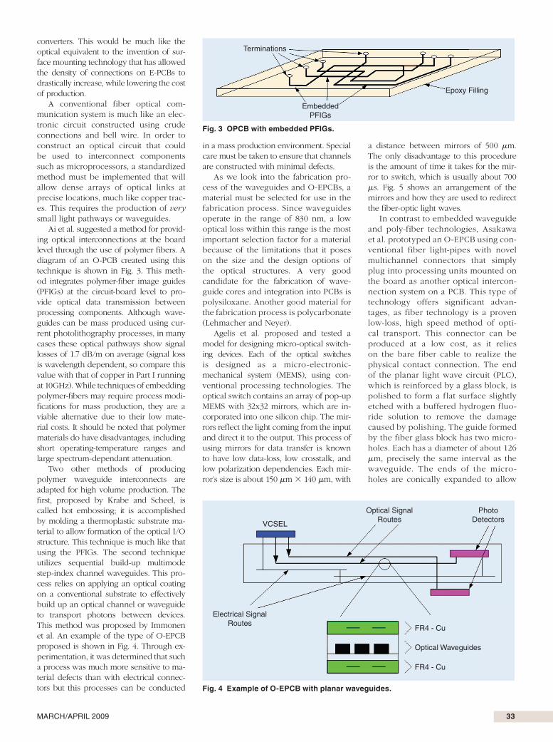
Ai et al. suggested a method for provid-ing optical interconnections at the board level through the use of polymer fibers. A diagram of an O-PCB created using this technique is shown in Fig. 3. This meth-od integrates polymer-fiber image guides (PFIGs) at the circuit-board level to pro-vide optical data transmission between processing components. Although wave-guides can be mass produced using cur-rent photolithography processes, in many cases these optical pathways show signal losses of 1.7 dB/m on average (signal loss is wavelength dependent, so compare this value with that of copper in Part I running at 10GHz). While techniques of embedding polymer-fibers may require process modi-fications for mass production, they are a viable alternative due to their low mate-rial costs. It should be noted that polymer materials do have disadvantages, including short operating-temperature ranges and large spectrum-dependant attenuation.
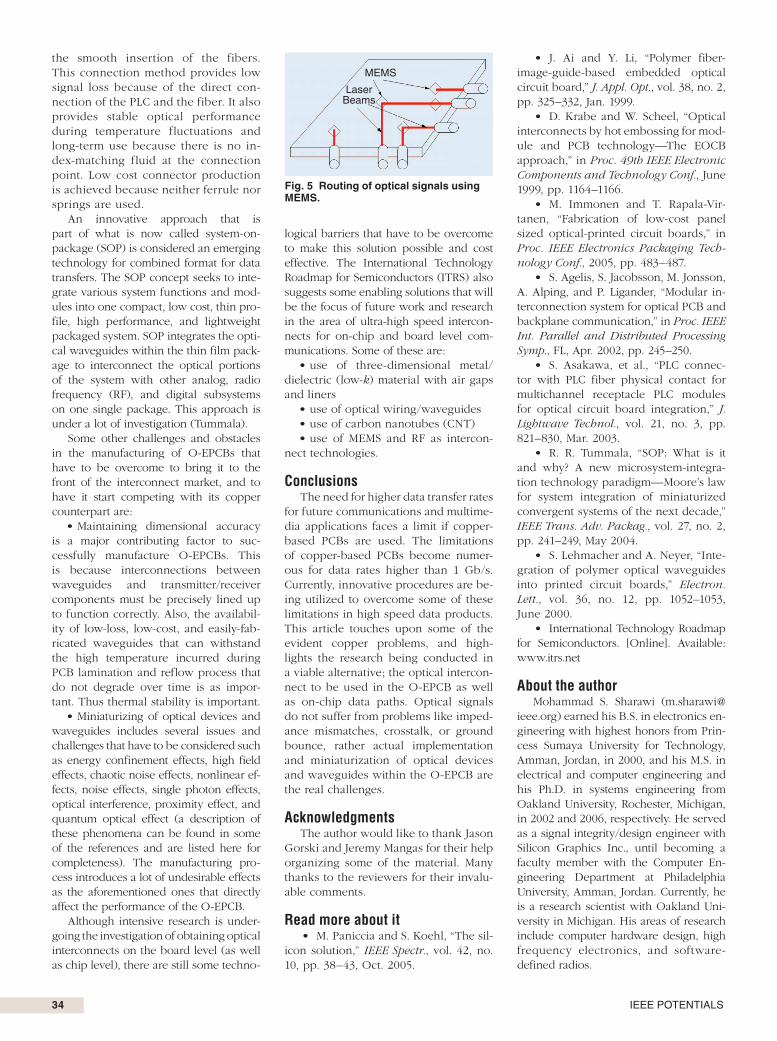
Two other methods of producing polymer waveguide interconnects are adapted for high volume production. The first, proposed by Krabe and Scheel, is called hot embossing; it is accomplished by molding a thermoplastic substrate ma-terial to allow formation of the optical I/O structure. This technique is much like that using the PFIGs. The second technique utilizes sequential build-up multimode step-index channel waveguides. This pro-cess relies on applying an optical coating on a conventional substrate to effectively build up an optical channel or waveguide to transport photons between devices. This method was proposed by Immonen et al. An example of the type of O-EPCB proposed is shown in Fig. 4. Through ex-perimentation, it was determined that such a process was much more sensitive to ma-terial defects than with electrical connec-tors but this processes can be conducted
in a mass production environment. Special care must be taken to ensure that channels are constructed with minimal defects.
As we look into the fabrication pro-cess of the waveguides and O-EPCBs, a material must be selected for use in the fabrication process. Since waveguides operate in the range of 830 nm, a low optical loss within this range is the most important selection factor for a material because of the limitations that it poses on the size and the design options of the optical structures. A very good candidate for the fabrication of wave-guide cores and integration into PCBs is polysiloxane. Another good material for the fabrication process is polycarbonate (Lehmacher and Neyer).
Agelis et al. proposed and tested a model for designing micro-optical switch-ing devices. Each of the optical switches is designed as a micro-electronic-mechanical system (MEMS), using con-ventional processing technologies. The optical switch contains an array of pop-up MEMS with 32x32 mirrors, which are in-corporated into one silicon chip. The mir-rors reflect the light coming from the input and direct it to the output. This process of using mirrors for data transfer is known to have low data-loss, low crosstalk, and low polarization dependencies. Each mir-ror’s size is about 150 mm 3 140 mm, with
a distance between mirrors of 500 mm. The only disadvantage to this procedure is the amount of time it takes for the mir-ror to switch, which is usually about 700 ms. Fig. 5 shows an arrangement of the mirrors and how they are used to redirect the fiber-optic light waves.
In contrast to embedded waveguide and poly-fiber technologies, Asakawa et al. prototyped an O-EPCB using con-ventional fiber light-pipes with novel multichannel connectors that simply plug into processing units mounted on the board as another optical intercon-nection system on a PCB. This type of technology offers significant advan-tages, as fiber technology is a proven low-loss, high speed method of opti-cal transport. This connector can be produced at a low cost, as it relies on the bare fiber cable to realize the physical contact connection. The end of the planar light wave circuit (PLC), which is reinforced by a glass block, is polished to form a flat surface slightly etched with a buffered hydrogen fluo-ride solution to remove the damage caused by polishing. The guide formed by the fiber glass block has two micro-holes. Each has a diameter of about 126 mm, precisely the same interval as the waveguide. The ends of the micro-holes are conically expanded to allow
Terminations
EmbeddedPFIGs
Epoxy Filling
Fig. 3 OPCB with embedded PFIGs.
VCSEL
Optical SignalRoutes
Electrical SignalRoutes
PhotoDetectors
FR4 - Cu
FR4 - Cu
Optical Waveguides
Fig. 4 Example of O-EPCB with planar waveguides.
34 IEEE POTENTIALS
the smooth insertion of the fibers. This connection method provides low signal loss because of the direct con-nection of the PLC and the fiber. It also provides stable optical performance during temperature fluctuations and long-term use because there is no in-dex-matching fluid at the connection point. Low cost connector production is achieved because neither ferrule nor springs are used.
An innovative approach that is part of what is now called system-on-package (SOP) is considered an emerging technology for combined format for data transfers. The SOP concept seeks to inte-grate various system functions and mod-ules into one compact, low cost, thin pro-file, high performance, and lightweight packaged system. SOP integrates the opti-cal waveguides within the thin film pack-age to interconnect the optical portions of the system with other analog, radio frequency (RF), and digital subsystems on one single package. This approach is under a lot of investigation (Tummala).
Some other challenges and obstacles in the manufacturing of O-EPCBs that have to be overcome to bring it to the front of the interconnect market, and to have it start competing with its copper counterpart are:
Maintaining dimensional accuracy •is a major contributing factor to suc-cessfully manufacture O-EPCBs. This is because interconnections between waveguides and transmitter/receiver components must be precisely lined up to function correctly. Also, the availabil-ity of low-loss, low-cost, and easily-fab-ricated waveguides that can withstand the high temperature incurred during PCB lamination and reflow process that do not degrade over time is as impor-tant. Thus thermal stability is important.
• Miniaturizing of optical devices and waveguides includes several issues and challenges that have to be considered such as energy confinement effects, high field effects, chaotic noise effects, nonlinear ef-fects, noise effects, single photon effects, optical interference, proximity effect, and quantum optical effect (a description of these phenomena can be found in some of the references and are listed here for completeness). The manufacturing pro-cess introduces a lot of undesirable effects as the aforementioned ones that directly affect the performance of the O-EPCB.
Although intensive research is under-going the investigation of obtaining optical interconnects on the board level (as well as chip level), there are still some techno-
logical barriers that have to be overcome to make this solution possible and cost effective. The International Technology Roadmap for Semiconductors (ITRS) also suggests some enabling solutions that will be the focus of future work and research in the area of ultra-high speed intercon-nects for on-chip and board level com-munications. Some of these are:
use of three-dimensional metal/ •dielectric (low-k) material with air gaps and liners
use of optical wiring/waveguides • use of carbon nanotubes (CNT) • use of MEMS and RF as intercon- •
nect technologies.
Conclusions The need for higher data transfer rates
for future communications and multime-dia applications faces a limit if copper-based PCBs are used. The limitations of copper-based PCBs become numer-ous for data rates higher than 1 Gb/s. Currently, innovative procedures are be-ing utilized to overcome some of these limitations in high speed data products. This article touches upon some of the evident copper problems, and high-lights the research being conducted in a viable alternative; the optical intercon-nect to be used in the O-EPCB as well as on-chip data paths. Optical signals do not suffer from problems like imped-ance mismatches, crosstalk, or ground bounce, rather actual implementation and miniaturization of optical devices and waveguides within the O-EPCB are the real challenges.
Acknowledgments The author would like to thank Jason
Gorski and Jeremy Mangas for their help organizing some of the material. Many thanks to the reviewers for their invalu-able comments.
Read more about it • M. Paniccia and S. Koehl , “ The sil-icon solution ,” IEEE Spectr. , vol. 42 , no. 10 , pp. 38 – 43 , Oct. 2005 .
• J. Ai and Y. Li , “ Polymer fiber-image-guide-based embedded optical circuit board ,” J. Appl. Opt. , vol. 38 , no. 2 , pp. 325 – 332 , Jan. 1999 . • D. Krabe and W. Scheel , “ Optical interconnects by hot embossing for mod-ule and PCB technology—The EOCB approach ,” in Proc. 49th IEEE Electronic Components and Technology Conf. , June 1999 , pp. 1164 – 1166 . • M. Immonen and T. Rapala-Vir-tanen , “ Fabrication of low-cost panel sized optical-printed circuit boards ,” in Proc. IEEE Electronics Packaging Tech-nology Conf. , 2005 , pp. 483 – 487 . • S. Agelis , S. Jacobsson , M. Jonsson , A. Alping , and P. Ligander , “ Modular in-terconnection system for optical PCB and backplane communication ,” in Proc. IEEE Int. Parallel and Distributed Processing Symp. , FL , Apr. 2002, pp. 245–250. • S. Asakawa , et al. , “ PLC connec-tor with PLC fiber physical contact for multichannel receptacle PLC modules for optical circuit board integration ,” J. Lightwave Technol. , vol. 21 , no. 3 , pp. 821 – 830 , Mar. 2003 . • R. R. Tummala , “ SOP: What is it and why? A new microsystem-integra-tion technology paradigm—Moore’s law for system integration of miniaturized convergent systems of the next decade ,” IEEE Trans. Adv. Packag. , vol. 27 , no. 2 , pp. 241 – 249 , May 2004 . • S. Lehmacher and A. Neyer , “ Inte-gration of polymer optical waveguides into printed circuit boards ,” Electron. Lett. , vol. 36 , no. 12 , pp. 1052 – 1053 , June 2000 . • International Technology Roadmap for Semiconductors. [Online]. Available: www.itrs.net About the author
Mohammad S. Sharawi ([email protected]) earned his B.S. in electronics en-gineering with highest honors from Prin-cess Sumaya University for Technology, Amman, Jordan, in 2000, and his M.S. in electrical and computer engineering and his Ph.D. in systems engineering from Oakland University, Rochester, Michigan, in 2002 and 2006, respectively. He served as a signal integrity/design engineer with Silicon Graphics Inc., until becoming a faculty member with the Computer En-gineering Department at Philadelphia University, Amman, Jordan. Currently, he is a research scientist with Oakland Uni-versity in Michigan. His areas of research include computer hardware design, high frequency electronics, and software- defined radios.
Fig. 5 Routing of optical signals using MEMS.
LaserBeams
MEMS