Opto Coupled Devices - Electronics...Opto Coupled Devices Module 5.0 Opto Devices & Phototransistors...
19
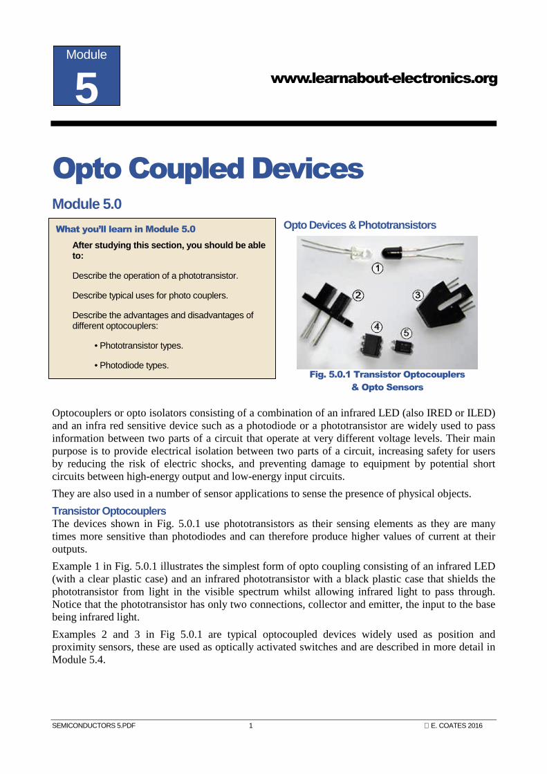
SEMICONDUCTORS 5.PDF 1 E. COATES 2016 Opto Coupled Devices Module 5.0 Opto Devices & Phototransistors Optocouplers or opto isolators consisting of a combination of an infrared LED (also IRED or ILED) and an infra red sensitive device such as a photodiode or a phototransistor are widely used to pass information between two parts of a circuit that operate at very different voltage levels. Their main purpose is to provide electrical isolation between two parts of a circuit, increasing safety for users by reducing the risk of electric shocks, and preventing damage to equipment by potential short circuits between high-energy output and low-energy input circuits. They are also used in a number of sensor applications to sense the presence of physical objects. Transistor Optocouplers The devices shown in Fig. 5.0.1 use phototransistors as their sensing elements as they are many times more sensitive than photodiodes and can therefore produce higher values of current at their outputs. Example 1 in Fig. 5.0.1 illustrates the simplest form of opto coupling consisting of an infrared LED (with a clear plastic case) and an infrared phototransistor with a black plastic case that shields the phototransistor from light in the visible spectrum whilst allowing infrared light to pass through. Notice that the phototransistor has only two connections, collector and emitter, the input to the base being infrared light. Examples 2 and 3 in Fig 5.0.1 are typical optocoupled devices widely used as position and proximity sensors, these are used as optically activated switches and are described in more detail in Module 5.4. www.learnabout-electronics.org Module 5 What you’ll learn in Module 5.0 After studying this section, you should be able to: Describe the operation of a phototransistor. Describe typical uses for photo couplers. Describe the advantages and disadvantages of different optocouplers: • Phototransistor types. • Photodiode types. Fig. 5.0.1 Transistor Optocouplers & Opto Sensors
Transcript of Opto Coupled Devices - Electronics...Opto Coupled Devices Module 5.0 Opto Devices & Phototransistors...
SEMICONDUCTORS 5.PDF 1 E. COATES 2016
Opto Coupled Devices Module 5.0
Opto Devices & Phototransistors
Optocouplers or opto isolators consisting of a combination of an infrared LED (also IRED or ILED) and an infra red sensitive device such as a photodiode or a phototransistor are widely used to pass information between two parts of a circuit that operate at very different voltage levels. Their main purpose is to provide electrical isolation between two parts of a circuit, increasing safety for users by reducing the risk of electric shocks, and preventing damage to equipment by potential short circuits between high-energy output and low-energy input circuits.
They are also used in a number of sensor applications to sense the presence of physical objects.
Transistor Optocouplers The devices shown in Fig. 5.0.1 use phototransistors as their sensing elements as they are many times more sensitive than photodiodes and can therefore produce higher values of current at their outputs.
Example 1 in Fig. 5.0.1 illustrates the simplest form of opto coupling consisting of an infrared LED (with a clear plastic case) and an infrared phototransistor with a black plastic case that shields the phototransistor from light in the visible spectrum whilst allowing infrared light to pass through. Notice that the phototransistor has only two connections, collector and emitter, the input to the base being infrared light.
Examples 2 and 3 in Fig 5.0.1 are typical optocoupled devices widely used as position and proximity sensors, these are used as optically activated switches and are described in more detail in Module 5.4.
www.learnabout-electronics.org
Module
5
What you’ll learn in Module 5.0
After studying this section, you should be able to:
Describe the operation of a phototransistor.
Describe typical uses for photo couplers.
Describe the advantages and disadvantages of different optocouplers:
• Phototransistor types.
• Photodiode types. Fig. 5.0.1 Transistor Optocouplers
& Opto Sensors
www.learnabout-electronics.org Semiconductors Module 5
SEMICONDUCTORS MODULE 5 PDF 2 E. COATES 2017
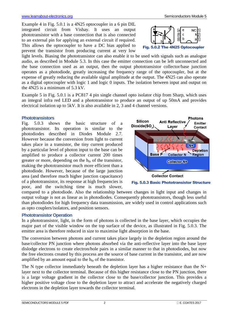
Example 4 in Fig. 5.0.1 is a 4N25 optocoupler in a 6 pin DIL integrated circuit from Vishay. It uses an output phototransistor with a base connection that is also connected to an external pin for applying an external circuit if required. This allows the optocoupler to have a DC bias applied to prevent the transistor from producing current at very low light levels. Biasing the phototransistor can also enable it to be used with signals such as analogue audio, as described in Module 5.3. In this case the emitter connection can be left unconnected and the base connection used as an output, then the output phototransistor collector/base junction operates as a photodiode, greatly increasing the frequency range of the optocoupler, but at the expense of greatly reducing the available signal amplitude at the output. The 4N25 can also operate as a digital optocoupler with logic 1 and logic 0 inputs. The isolation between input and output on the 4N25 is a minimum of 5.3 kV.
Example 5 in Fig. 5.0.1 is a PC817 4 pin single channel opto isolator chip from Sharp, which uses an integral infra red LED and a phototransistor to produce an output of up 50mA and provides electrical isolation up to 5kV. It is also available in 2, 3 and 4 channel versions.
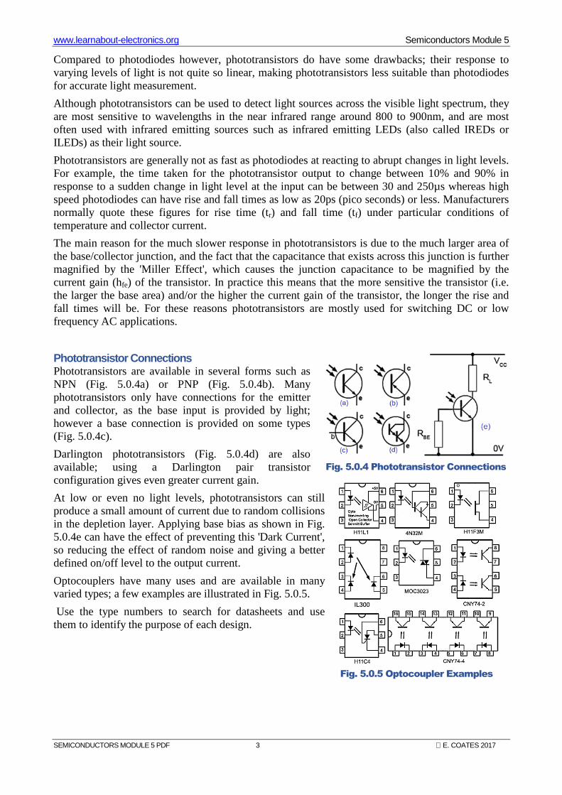
Phototransistors Fig. 5.0.3 shows the basic structure of a phototransistor. Its operation is similar to the photodiodes described in Diodes Module 2.7. However because the conversion from light to current takes place in a transistor, the tiny current produced by a particular level of photon input to the base can be amplified to produce a collector current 200 times greater or more, depending on the hfe of the transistor, making the phototransistor much more efficient than a photodiode. However, because of the large junction area (and therefore much higher junction capacitance) of a phototransistor, its response at high frequencies is poor, and the switching time is much slower, compared to a photodiode. Also the relationship between changes in light input and changes in output voltage is not as linear as in photodiodes. Consequently phototransistors, though less useful than photodiodes for high frequency data transmission, are widely used in control applications such as opto couplers/isolators, and position sensors.
Phototransistor Operation In a phototransistor, light, in the form of photons is collected in the base layer, which occupies the major part of the visible window on the top surface of the device, as illustrated in Fig. 5.0.3. The emitter area is therefore reduced in size to maximise light absorption in the base.
The conversion between photons and current takes place largely in the depletion region around the base/collector PN junction where photons absorbed via the anti-reflective layer into the base layer dislodge electrons to create electron/hole pairs in a similar manner to that in photodiodes, but now the free electrons created by this process are the source of base current in the transistor, and are now amplified by an amount equal to the hfe of the transistor.
The N type collector immediately beneath the depletion layer has a higher resistance than the N+ layer next to the collector terminal. Because of this higher resistance close to the PN junction, there is a large voltage gradient in the collector close to the base/collector junction. This provides a higher positive voltage close to the depletion layer to attract and accelerate the negatively charged electrons in the depletion layer towards the collector terminal.
Fig. 5.0.2 The 4N25 Optocoupler
Fig. 5.0.3 Basic Phototransistor Structure
www.learnabout-electronics.org Semiconductors Module 5
SEMICONDUCTORS MODULE 5 PDF 3 E. COATES 2017
Compared to photodiodes however, phototransistors do have some drawbacks; their response to varying levels of light is not quite so linear, making phototransistors less suitable than photodiodes for accurate light measurement.
Although phototransistors can be used to detect light sources across the visible light spectrum, they are most sensitive to wavelengths in the near infrared range around 800 to 900nm, and are most often used with infrared emitting sources such as infrared emitting LEDs (also called IREDs or ILEDs) as their light source.
Phototransistors are generally not as fast as photodiodes at reacting to abrupt changes in light levels. For example, the time taken for the phototransistor output to change between 10% and 90% in response to a sudden change in light level at the input can be between 30 and 250µs whereas high speed photodiodes can have rise and fall times as low as 20ps (pico seconds) or less. Manufacturers normally quote these figures for rise time (tr) and fall time (tf) under particular conditions of temperature and collector current.
The main reason for the much slower response in phototransistors is due to the much larger area of the base/collector junction, and the fact that the capacitance that exists across this junction is further magnified by the 'Miller Effect', which causes the junction capacitance to be magnified by the current gain (hfe) of the transistor. In practice this means that the more sensitive the transistor (i.e. the larger the base area) and/or the higher the current gain of the transistor, the longer the rise and fall times will be. For these reasons phototransistors are mostly used for switching DC or low frequency AC applications.
Phototransistor Connections Phototransistors are available in several forms such as NPN (Fig. 5.0.4a) or PNP (Fig. 5.0.4b). Many phototransistors only have connections for the emitter and collector, as the base input is provided by light; however a base connection is provided on some types (Fig. 5.0.4c).
Darlington phototransistors (Fig. 5.0.4d) are also available; using a Darlington pair transistor configuration gives even greater current gain.
At low or even no light levels, phototransistors can still produce a small amount of current due to random collisions in the depletion layer. Applying base bias as shown in Fig. 5.0.4e can have the effect of preventing this 'Dark Current', so reducing the effect of random noise and giving a better defined on/off level to the output current.
Optocouplers have many uses and are available in many varied types; a few examples are illustrated in Fig. 5.0.5.
Use the type numbers to search for datasheets and use them to identify the purpose of each design.
Fig. 5.0.4 Phototransistor Connections
Fig. 5.0.5 Optocoupler Examples
www.learnabout-electronics.org Semiconductors Module 5
SEMICONDUCTORS MODULE 5 PDF 4 E. COATES 2017
Module 5.1 Optocoupler Operation
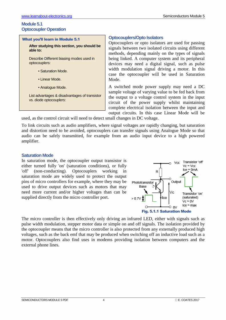
Optocouplers/Opto Isolators Optocouplers or opto isolators are used for passing signals between two isolated circuits using different methods, depending mainly on the types of signals being linked. A computer system and its peripheral devices may need a digital signal, such as pulse width modulation signal driving a motor. In this case the optocoupler will be used in Saturation Mode.
A switched mode power supply may need a DC sample voltage of varying value to be fed back from the output to a voltage control system in the input circuit of the power supply whilst maintaining complete electrical isolation between the input and output circuits. In this case Linear Mode will be
used, as the control circuit will need to detect small changes in DC voltage.
To link circuits such as audio amplifiers, where signal voltages are rapidly changing, but saturation and distortion need to be avoided, optocouplers can transfer signals using Analogue Mode so that audio can be safely transmitted, for example from an audio input device to a high powered amplifier.
Saturation Mode In saturation mode, the optocoupler output transistor is either turned fully 'on' (saturation conditions), or fully 'off' (non-conducting). Optocouplers working in saturation mode are widely used to protect the output pins of micro controllers for example, where they may be used to drive output devices such as motors that may need more current and/or higher voltages than can be supplied directly from the micro controller port.
The micro controller is then effectively only driving an infrared LED, either with signals such as pulse width modulation, stepper motor data or simple on and off signals. The isolation provided by the optocoupler means that the micro controller is also protected from any externally produced high voltages, such as the back emf that may be produced when switching off an inductive load such as a motor. Optocouplers also find uses in modems providing isolation between computers and the external phone lines.
What you’ll learn in Module 5.1
After studying this section, you should be able to:
Describe Different biasing modes used in optocouplers:
• Saturation Mode.
• Linear Mode.
• Analogue Mode.
List advantages & disadvantages of transistor vs. diode optocouplers:
Fig. 5.1.1 Saturation Mode
www.learnabout-electronics.org Semiconductors Module 5
SEMICONDUCTORS MODULE 5 PDF 5 E. COATES 2017
Linear Mode
Optocouplers can be used for voltage feedback in circuits such as switched mode power supplies, where the LED is illuminated by a sample of the output voltage so that any voltage variations cause a variation in the illumination of the optocoupler LED and therefore a variation in the conduction of the optocoupler’s output transistor, that can be used to signify an error to the power supply control circuitry, allowing it to compensate for the output variation. A practical example of this feedback and the electrical isolation it provides by using an optocoupler in linear mode can be seen in our Power Supplies Module 3.4 where IC3 (a 4N25) provides a sample of the output voltage to be fed back to an error amplifier controlling the voltage regulator circuit within IC1, providing automatic voltage control, whilst giving complete electrical isolation between the 5V DC output circuit and the higher voltage input circuit.
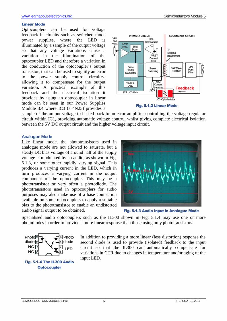
Analogue Mode Like linear mode, the phototransistors used in analogue mode are not allowed to saturate, but a steady DC bias voltage of around half of the supply voltage is modulated by an audio, as shown in Fig. 5.1.3, or some other rapidly varying signal. This produces a varying current in the LED, which in turn produces a varying current in the output component of the optocoupler. This may be a phototransistor or very often a photodiode. The phototransistors used in optocouplers for audio purposes may also make use of a base connection available on some optocouplers to apply a suitable bias to the phototransistor to enable an undistorted audio signal output to be obtained.
Specialised audio optocouplers such as the IL300 shown in Fig. 5.1.4 may use one or more photodiodes in order to provide a more linear response than those using only phototransistors.
In addition to providing a more linear (less distortion) response the second diode is used to provide (isolated) feedback to the input circuit so that the IL300 can automatically compensate for variations in CTR due to changes in temperature and/or aging of the input LED.
Fig. 5.1.2 Linear Mode
Fig. 5.1.3 Audio Input in Analogue Mode
Fig. 5.1.4 The IL300 Audio
Optocoupler
www.learnabout-electronics.org Semiconductors Module 5
SEMICONDUCTORS MODULE 5 PDF 6 E. COATES 2017
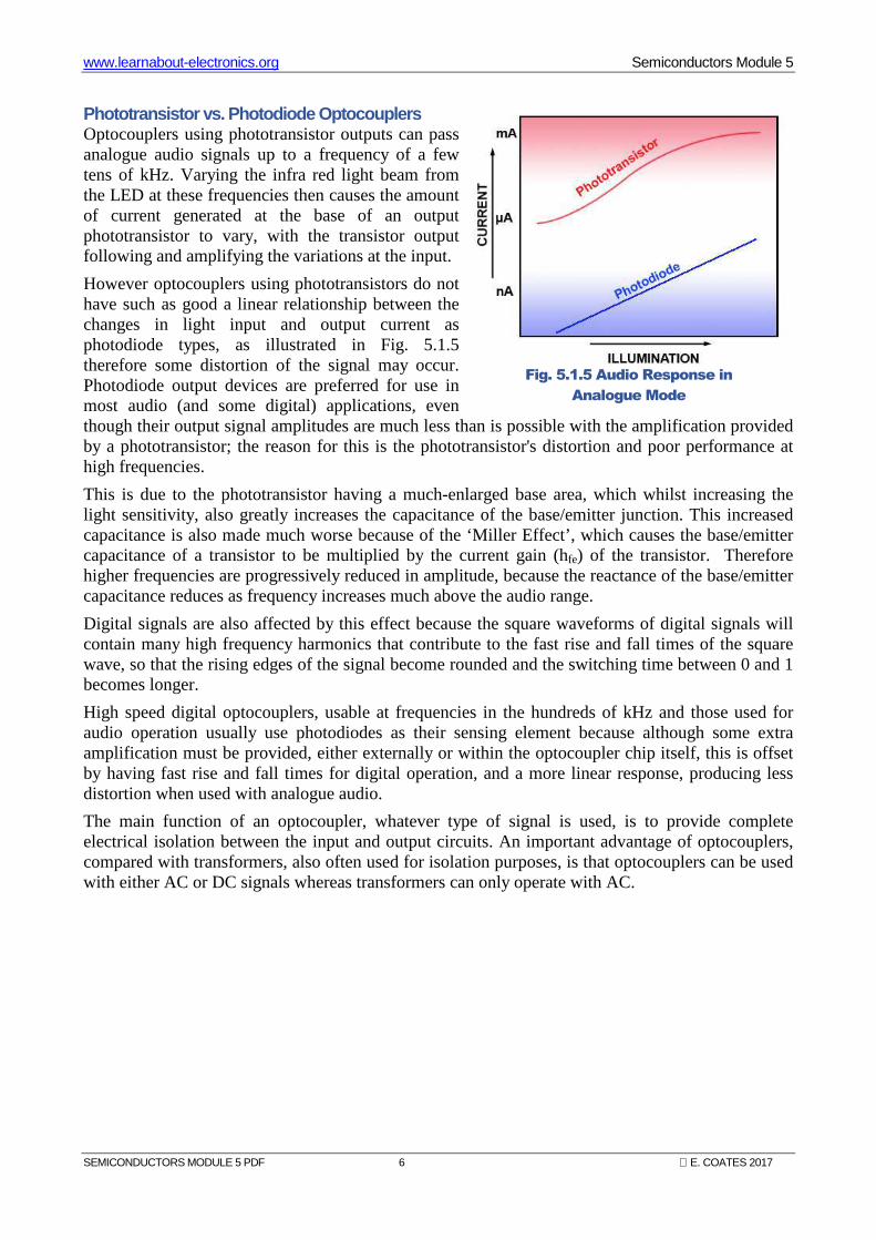
Phototransistor vs. Photodiode Optocouplers Optocouplers using phototransistor outputs can pass analogue audio signals up to a frequency of a few tens of kHz. Varying the infra red light beam from the LED at these frequencies then causes the amount of current generated at the base of an output phototransistor to vary, with the transistor output following and amplifying the variations at the input.
However optocouplers using phototransistors do not have such as good a linear relationship between the changes in light input and output current as photodiode types, as illustrated in Fig. 5.1.5 therefore some distortion of the signal may occur. Photodiode output devices are preferred for use in most audio (and some digital) applications, even though their output signal amplitudes are much less than is possible with the amplification provided by a phototransistor; the reason for this is the phototransistor's distortion and poor performance at high frequencies.
This is due to the phototransistor having a much-enlarged base area, which whilst increasing the light sensitivity, also greatly increases the capacitance of the base/emitter junction. This increased capacitance is also made much worse because of the ‘Miller Effect’, which causes the base/emitter capacitance of a transistor to be multiplied by the current gain (hfe) of the transistor. Therefore higher frequencies are progressively reduced in amplitude, because the reactance of the base/emitter capacitance reduces as frequency increases much above the audio range.
Digital signals are also affected by this effect because the square waveforms of digital signals will contain many high frequency harmonics that contribute to the fast rise and fall times of the square wave, so that the rising edges of the signal become rounded and the switching time between 0 and 1 becomes longer.
High speed digital optocouplers, usable at frequencies in the hundreds of kHz and those used for audio operation usually use photodiodes as their sensing element because although some extra amplification must be provided, either externally or within the optocoupler chip itself, this is offset by having fast rise and fall times for digital operation, and a more linear response, producing less distortion when used with analogue audio.
The main function of an optocoupler, whatever type of signal is used, is to provide complete electrical isolation between the input and output circuits. An important advantage of optocouplers, compared with transformers, also often used for isolation purposes, is that optocouplers can be used with either AC or DC signals whereas transformers can only operate with AC.
Fig. 5.1.5 Audio Response in
Analogue Mode
www.learnabout-electronics.org Semiconductors Module 5
SEMICONDUCTORS MODULE 5 PDF 7 E. COATES 2017
Module 5.2 Using Optocouplers
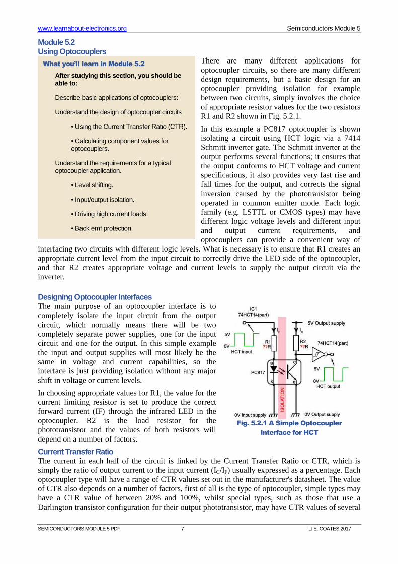
There are many different applications for optocoupler circuits, so there are many different design requirements, but a basic design for an optocoupler providing isolation for example between two circuits, simply involves the choice of appropriate resistor values for the two resistors R1 and R2 shown in Fig. 5.2.1.
In this example a PC817 optocoupler is shown isolating a circuit using HCT logic via a 7414 Schmitt inverter gate. The Schmitt inverter at the output performs several functions; it ensures that the output conforms to HCT voltage and current specifications, it also provides very fast rise and fall times for the output, and corrects the signal inversion caused by the phototransistor being operated in common emitter mode. Each logic family (e.g. LSTTL or CMOS types) may have different logic voltage levels and different input and output current requirements, and optocouplers can provide a convenient way of
interfacing two circuits with different logic levels. What is necessary is to ensure that R1 creates an appropriate current level from the input circuit to correctly drive the LED side of the optocoupler, and that R2 creates appropriate voltage and current levels to supply the output circuit via the inverter.
Designing Optocoupler Interfaces The main purpose of an optocoupler interface is to completely isolate the input circuit from the output circuit, which normally means there will be two completely separate power supplies, one for the input circuit and one for the output. In this simple example the input and output supplies will most likely be the same in voltage and current capabilities, so the interface is just providing isolation without any major shift in voltage or current levels.
In choosing appropriate values for R1, the value for the current limiting resistor is set to produce the correct forward current (IF) through the infrared LED in the optocoupler. R2 is the load resistor for the phototransistor and the values of both resistors will depend on a number of factors.
Current Transfer Ratio The current in each half of the circuit is linked by the Current Transfer Ratio or CTR, which is simply the ratio of output current to the input current (IC/IF) usually expressed as a percentage. Each optocoupler type will have a range of CTR values set out in the manufacturer's datasheet. The value of CTR also depends on a number of factors, first of all is the type of optocoupler, simple types may have a CTR value of between 20% and 100%, whilst special types, such as those that use a Darlington transistor configuration for their output phototransistor, may have CTR values of several
What you’ll learn in Module 5.2
After studying this section, you should be able to:
Describe basic applications of optocouplers:
Understand the design of optocoupler circuits
• Using the Current Transfer Ratio (CTR).
• Calculating component values for optocouplers.
Understand the requirements for a typical optocoupler application.
• Level shifting.
• Input/output isolation.
• Driving high current loads.
• Back emf protection.
Fig. 5.2.1 A Simple Optocoupler
Interface for HCT
www.learnabout-electronics.org Semiconductors Module 5
SEMICONDUCTORS MODULE 5 PDF 8 E. COATES 2017
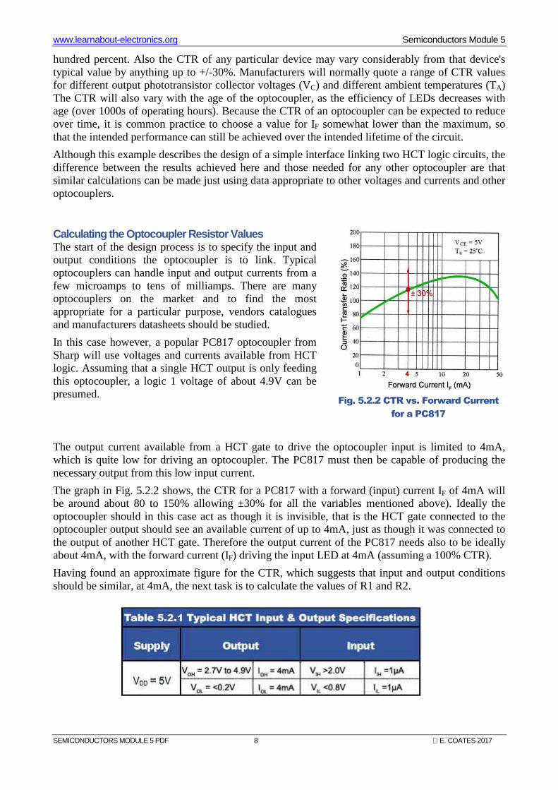
hundred percent. Also the CTR of any particular device may vary considerably from that device's typical value by anything up to +/-30%. Manufacturers will normally quote a range of CTR values for different output phototransistor collector voltages (VC) and different ambient temperatures (TA) The CTR will also vary with the age of the optocoupler, as the efficiency of LEDs decreases with age (over 1000s of operating hours). Because the CTR of an optocoupler can be expected to reduce over time, it is common practice to choose a value for IF somewhat lower than the maximum, so that the intended performance can still be achieved over the intended lifetime of the circuit.
Although this example describes the design of a simple interface linking two HCT logic circuits, the difference between the results achieved here and those needed for any other optocoupler are that similar calculations can be made just using data appropriate to other voltages and currents and other optocouplers.
Calculating the Optocoupler Resistor Values The start of the design process is to specify the input and output conditions the optocoupler is to link. Typical optocouplers can handle input and output currents from a few microamps to tens of milliamps. There are many optocouplers on the market and to find the most appropriate for a particular purpose, vendors catalogues and manufacturers datasheets should be studied.
In this case however, a popular PC817 optocoupler from Sharp will use voltages and currents available from HCT logic. Assuming that a single HCT output is only feeding this optocoupler, a logic 1 voltage of about 4.9V can be presumed.
The output current available from a HCT gate to drive the optocoupler input is limited to 4mA, which is quite low for driving an optocoupler. The PC817 must then be capable of producing the necessary output from this low input current.
The graph in Fig. 5.2.2 shows, the CTR for a PC817 with a forward (input) current IF of 4mA will be around about 80 to 150% allowing ±30% for all the variables mentioned above). Ideally the optocoupler should in this case act as though it is invisible, that is the HCT gate connected to the optocoupler output should see an available current of up to 4mA, just as though it was connected to the output of another HCT gate. Therefore the output current of the PC817 needs also to be ideally about 4mA, with the forward current (IF) driving the input LED at 4mA (assuming a 100% CTR).
Having found an approximate figure for the CTR, which suggests that input and output conditions should be similar, at 4mA, the next task is to calculate the values of R1 and R2.
Fig. 5.2.2 CTR vs. Forward Current
for a PC817
www.learnabout-electronics.org Semiconductors Module 5
SEMICONDUCTORS MODULE 5 PDF 9 E. COATES 2017
Using the data in Table 5.2.1 and assuming minimum 4.9V to 5V input at the HCT gate output, it is possible to calculate a suitable resistance value for R1 in Fig.5.2.3.
The forward Voltage across the infrared LED with a forward current of only 4mA should be about 1.2V
5V − 1.2V = 3.8V to be developed across R1
Therefore R1 = 3.8V÷4mA = 950Ω
Using the next higher preferred resistor value
R1 = 1KΩ
The graph of CTR vs. IF in Fig. 5.2.2 shows that ideally the CTR for the PC817 will be about 115% with a forward current of 4mA, which suggests that the opto output current should be about 4mA x 115% = 4.6mA
To saturate the phototransistor and produce a logic 0 (less than 0.2V) at the output, R2 must develop a voltage of 4.9 to 5V when passing a current of 4.6mA (assuming 115% CTR value).
R2 must therefore be at least 5V÷4.6mA = 1087Ω
or R2 = 1.2kΩ (next preferred value).
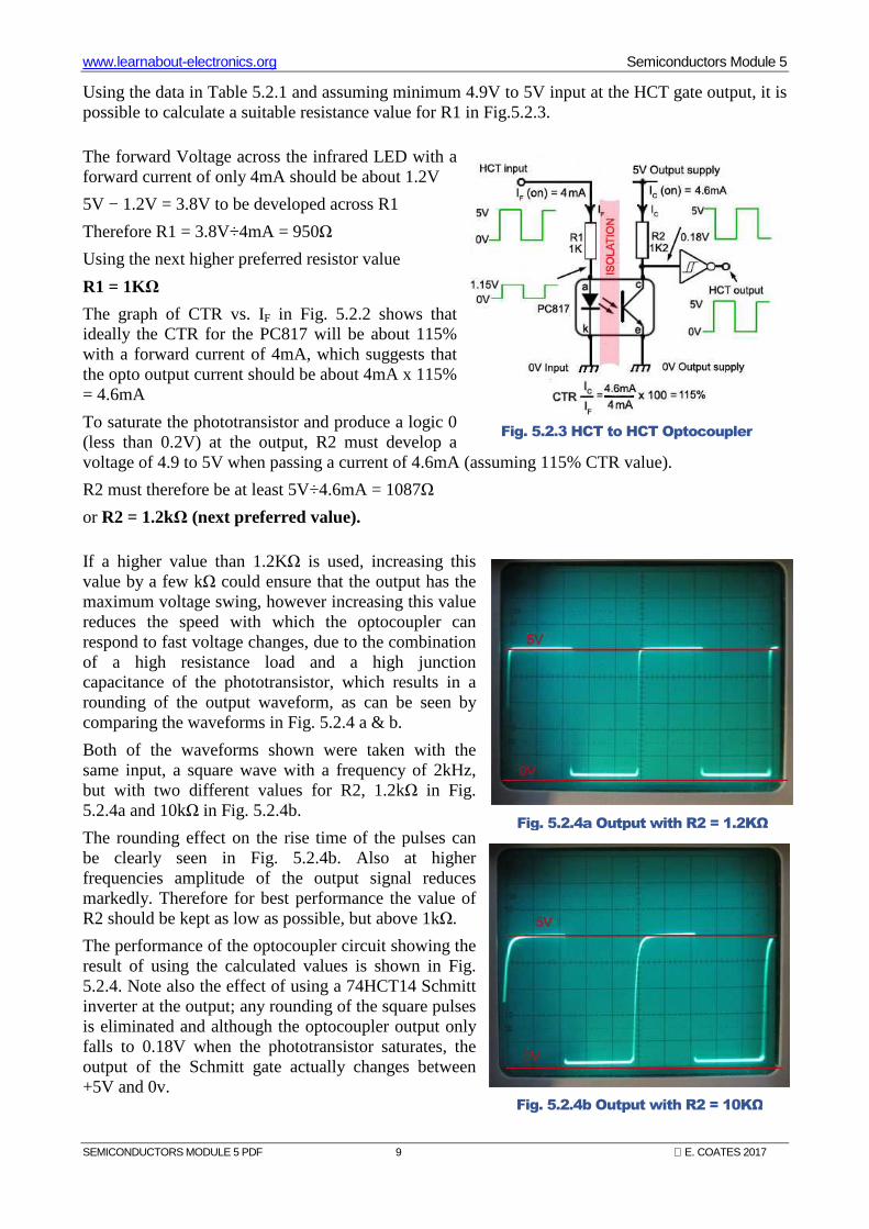
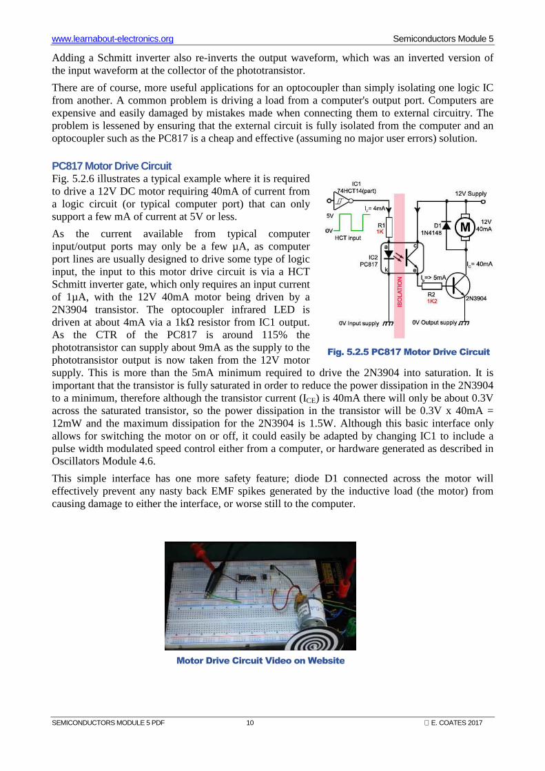
If a higher value than 1.2KΩ is used, increasing this value by a few kΩ could ensure that the output has the maximum voltage swing, however increasing this value reduces the speed with which the optocoupler can respond to fast voltage changes, due to the combination of a high resistance load and a high junction capacitance of the phototransistor, which results in a rounding of the output waveform, as can be seen by comparing the waveforms in Fig. 5.2.4 a & b.
Both of the waveforms shown were taken with the same input, a square wave with a frequency of 2kHz, but with two different values for R2, 1.2kΩ in Fig. 5.2.4a and 10kΩ in Fig. 5.2.4b.
The rounding effect on the rise time of the pulses can be clearly seen in Fig. 5.2.4b. Also at higher frequencies amplitude of the output signal reduces markedly. Therefore for best performance the value of R2 should be kept as low as possible, but above 1kΩ.
The performance of the optocoupler circuit showing the result of using the calculated values is shown in Fig. 5.2.4. Note also the effect of using a 74HCT14 Schmitt inverter at the output; any rounding of the square pulses is eliminated and although the optocoupler output only falls to 0.18V when the phototransistor saturates, the output of the Schmitt gate actually changes between +5V and 0v.
Fig. 5.2.3 HCT to HCT Optocoupler
Fig. 5.2.4a Output with R2 = 1.2KΩ
Fig. 5.2.4b Output with R2 = 10KΩ
www.learnabout-electronics.org Semiconductors Module 5
SEMICONDUCTORS MODULE 5 PDF 10 E. COATES 2017
Adding a Schmitt inverter also re-inverts the output waveform, which was an inverted version of the input waveform at the collector of the phototransistor.
There are of course, more useful applications for an optocoupler than simply isolating one logic IC from another. A common problem is driving a load from a computer's output port. Computers are expensive and easily damaged by mistakes made when connecting them to external circuitry. The problem is lessened by ensuring that the external circuit is fully isolated from the computer and an optocoupler such as the PC817 is a cheap and effective (assuming no major user errors) solution.
PC817 Motor Drive Circuit Fig. 5.2.6 illustrates a typical example where it is required to drive a 12V DC motor requiring 40mA of current from a logic circuit (or typical computer port) that can only support a few mA of current at 5V or less.
As the current available from typical computer input/output ports may only be a few µA, as computer port lines are usually designed to drive some type of logic input, the input to this motor drive circuit is via a HCT Schmitt inverter gate, which only requires an input current of 1µA, with the 12V 40mA motor being driven by a 2N3904 transistor. The optocoupler infrared LED is driven at about 4mA via a 1kΩ resistor from IC1 output. As the CTR of the PC817 is around 115% the phototransistor can supply about 9mA as the supply to the phototransistor output is now taken from the 12V motor supply. This is more than the 5mA minimum required to drive the 2N3904 into saturation. It is important that the transistor is fully saturated in order to reduce the power dissipation in the 2N3904 to a minimum, therefore although the transistor current (ICE) is 40mA there will only be about 0.3V across the saturated transistor, so the power dissipation in the transistor will be 0.3V x 40mA = 12mW and the maximum dissipation for the 2N3904 is 1.5W. Although this basic interface only allows for switching the motor on or off, it could easily be adapted by changing IC1 to include a pulse width modulated speed control either from a computer, or hardware generated as described in Oscillators Module 4.6.
This simple interface has one more safety feature; diode D1 connected across the motor will effectively prevent any nasty back EMF spikes generated by the inductive load (the motor) from causing damage to either the interface, or worse still to the computer.
Fig. 5.2.5 PC817 Motor Drive Circuit
Motor Drive Circuit Video on Website
www.learnabout-electronics.org Semiconductors Module 5
SEMICONDUCTORS MODULE 5 PDF 11 E. COATES 2017
Module 5.3 Opto Coupled Devices
Audio Optocouplers In audio systems, isolation between inputs and higher voltage/current equipment is usually provided by audio transformers, however it is also possible to use specialised audio optocouplers such as the IL300, which uses an infra red LED to illuminate one photodiode as an output device and a second photodiode to provide feedback, ensuring improved linearity and wider frequency range than phototransistor or photo resistor alternatives. Using feedback from a second photodiode with characteristics closely matched to those of the output photodiode also overcomes a basic problem with
optocouplers. Without some sort of feedback, variations in the current transfer ratio will affect the performance of the optocoupler.
Variations can occur due to changes in ambient temperature and to ageing of the infrared LED. Optocouplers such as the IL300 from Vishay illustrated in Fig. 5.3.1 can therefore claim both better performance and stability over the lifetime of the circuit. Consequently these specialised devices are considerably more expensive than simple general-purpose optocouplers.
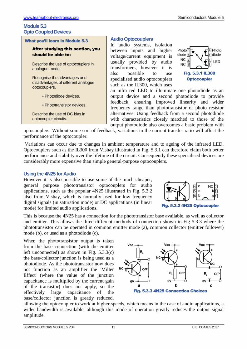
Using the 4N25 for Audio However it is also possible to use some of the much cheaper, general purpose phototransistor optocouplers for audio applications, such as the popular 4N25 illustrated in Fig. 5.3.2 also from Vishay, which is normally used for low frequency digital signals (in saturation mode) or DC applications (in linear mode) for limited audio applications.
This is because the 4N25 has a connection for the phototransistor base available, as well as collector and emitter. This allows the three different methods of connection shown in Fig 5.3.3 where the phototransistor can be operated in common emitter mode (a), common collector (emitter follower) mode (b), or used as a photodiode (c).
When the phototransistor output is taken from the base connection (with the emitter left unconnected) as shown in Fig. 5.3.3(c) the base/collector junction is being used as a photodiode. As the phototransistor now does not function as an amplifier the 'Miller Effect' (where the value of the junction capacitance is multiplied by the current gain of the transistor) does not apply, so the effectively large capacitance of the base/collector junction is greatly reduced, allowing the optocoupler to work at higher speeds, which means in the case of audio applications, a wider bandwidth is available, although this mode of operation greatly reduces the output signal amplitude.
What you’ll learn in Module 5.3
After studying this section, you
should be able to:
Describe the use of optocouplers in analogue mode:
Recognise the advantages and disadvantages of different analogue optocouplers.
• Photodiode devices.
• Phototransistor devices.
Describe the use of DC bias in optocoupler circuits.
Fig. 5.3.1 IL300
Optocoupler
Fig. 5.3.2 4N25 Optocoupler
Fig. 5.3.3 4N25 Connection Choices
www.learnabout-electronics.org Semiconductors Module 5
SEMICONDUCTORS MODULE 5 PDF 12 E. COATES 2017
In any of the configurations shown in Fig 5.3.3, the choice of load resistor has a significant effect on the output signal; the higher the value of RL the greater the amplitude of the output signal but the narrower the bandwidth, so the value of RL chosen is a compromise that depends on the purpose of the circuit.
For the 4N25 to provide isolation for audio signals the input to the infrared LED must be appropriately biased with a DC voltage, so that when a modulating AC (audio) signal is applied, the current through the LED can be varied without the optocoupler output reaching either saturation or cut off. This is really an extension of the linear mode of operation, and can be applied using either one of two basic configurations, phototransistor or photodiode.
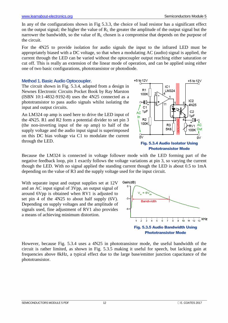
Method 1. Basic Audio Optocoupler. The circuit shown in Fig. 5.3.4, adapted from a design in Newnes Electronic Circuits Pocket Book by Ray Marston (ISBN 10:1-4832-9192-8) uses the 4N25 connected as a phototransistor to pass audio signals whilst isolating the input and output circuits.
An LM324 op amp is used here to drive the LED input of the 4N25. R1 and R2 form a potential divider to set pin 3 (the non-inverting input of the op amp) to half of the supply voltage and the audio input signal is superimposed on this DC bias voltage via C1 to modulate the current through the LED.
Because the LM324 is connected in voltage follower mode with the LED forming part of the negative feedback loop, pin 1 exactly follows the voltage variations at pin 3, so varying the current though the LED. With no signal applied the standing current though the LED is about 0.5 to 1mA depending on the value of R3 and the supply voltage used for the input circuit.
With separate input and output supplies set at 12V and an AC input signal of 3Vpp, an output signal of around 6Vpp is obtained when RV1 is adjusted to set pin 4 of the 4N25 to about half supply (6V). Depending on supply voltages and the amplitude of signals used, fine adjustment of RV1 also provides a means of achieving minimum distortion.
However, because Fig. 5.3.4 uses a 4N25 in phototransistor mode, the useful bandwidth of the circuit is rather limited, as shown in Fig. 5.3.5 making it useful for speech, but lacking gain at frequencies above 8kHz, a typical effect due to the large base/emitter junction capacitance of the phototransistor.
Fig. 5.3.4 Audio Isolator Using
Phototransistor Mode
Fig. 5.3.5 Audio Bandwidth Using
Phototransistor Mode
www.learnabout-electronics.org Semiconductors Module 5
SEMICONDUCTORS MODULE 5 PDF 13 E. COATES 2017
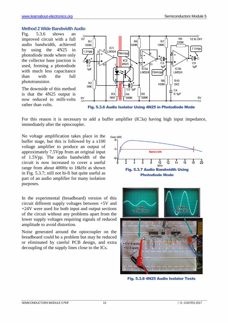
Method 2 Wide Bandwidth Audio Fig. 5.3.6 shows an improved circuit with a full audio bandwidth, achieved by using the 4N25 in photodiode mode where only the collector base junction is used, forming a photodiode with much less capacitance than with the full phototransistor.
The downside of this method is that the 4N25 output is now reduced to milli-volts rather than volts.
For this reason it is necessary to add a buffer amplifier (IC3a) having high input impedance, immediately after the optocoupler.
No voltage amplification takes place in the buffer stage, but this is followed by a x100 voltage amplifier to produce an output of approximately 7.5Vpp from an original input of 1.5Vpp. The audio bandwidth of the circuit is now increased to cover a useful range from about 400Hz to 18kHz as shown in Fig. 5.3.7; still not hi-fi but quite useful as part of an audio amplifier for many isolation purposes.
In the experimental (breadboard) version of this circuit different supply voltages between +5V and +24V were used for both input and output sections of the circuit without any problems apart from the lower supply voltages requiring signals of reduced amplitude to avoid distortion.
Noise generated around the optocoupler on the breadboard could be a problem but may be reduced or eliminated by careful PCB design, and extra decoupling of the supply lines close to the ICs.
Fig. 5.3.6 Audio Isolator Using 4N25 in Photodiode Mode
Fig. 5.3.7 Audio Bandwidth Using
Photodiode Mode
Fig. 5.3.8 4N25 Audio Isolator Tests
www.learnabout-electronics.org Semiconductors Module 5
SEMICONDUCTORS MODULE 5 PDF 14 E. COATES 2017
Module 5.4 Opto Activated Switches
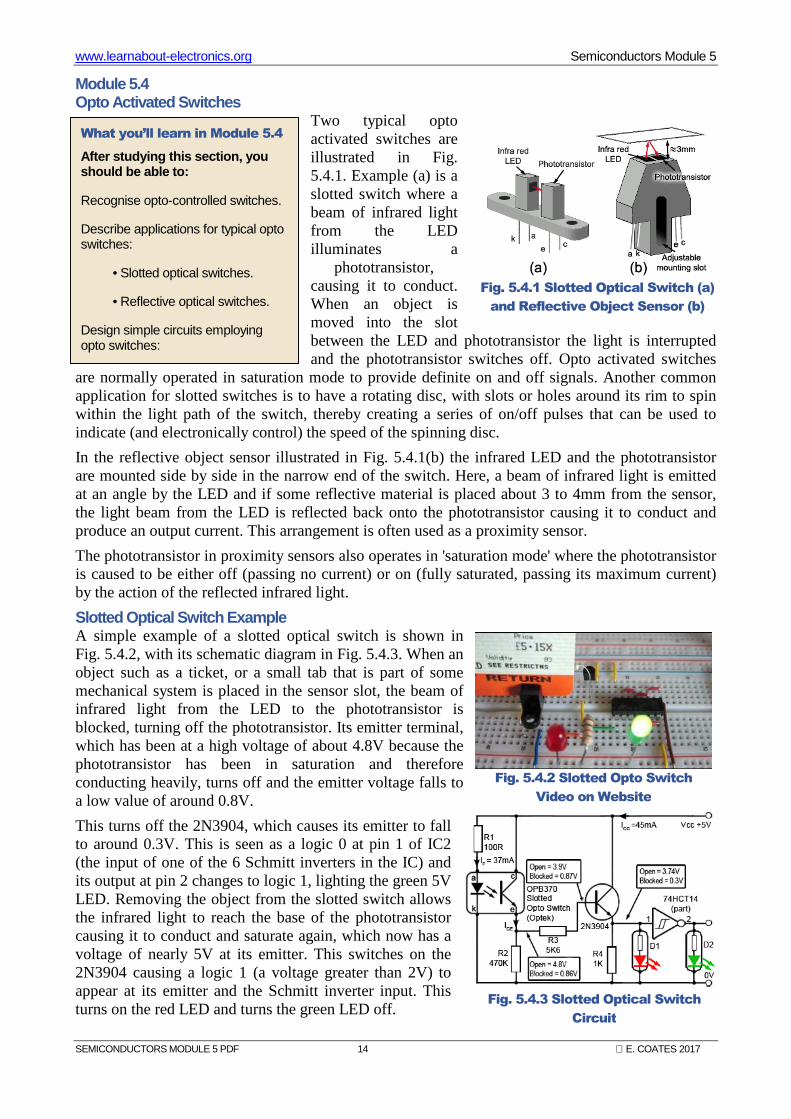
Two typical opto activated switches are illustrated in Fig. 5.4.1. Example (a) is a slotted switch where a beam of infrared light from the LED illuminates a
phototransistor, causing it to conduct. When an object is moved into the slot between the LED and phototransistor the light is interrupted and the phototransistor switches off. Opto activated switches
are normally operated in saturation mode to provide definite on and off signals. Another common application for slotted switches is to have a rotating disc, with slots or holes around its rim to spin within the light path of the switch, thereby creating a series of on/off pulses that can be used to indicate (and electronically control) the speed of the spinning disc.
In the reflective object sensor illustrated in Fig. 5.4.1(b) the infrared LED and the phototransistor are mounted side by side in the narrow end of the switch. Here, a beam of infrared light is emitted at an angle by the LED and if some reflective material is placed about 3 to 4mm from the sensor, the light beam from the LED is reflected back onto the phototransistor causing it to conduct and produce an output current. This arrangement is often used as a proximity sensor.
The phototransistor in proximity sensors also operates in 'saturation mode' where the phototransistor is caused to be either off (passing no current) or on (fully saturated, passing its maximum current) by the action of the reflected infrared light.
Slotted Optical Switch Example A simple example of a slotted optical switch is shown in Fig. 5.4.2, with its schematic diagram in Fig. 5.4.3. When an object such as a ticket, or a small tab that is part of some mechanical system is placed in the sensor slot, the beam of infrared light from the LED to the phototransistor is blocked, turning off the phototransistor. Its emitter terminal, which has been at a high voltage of about 4.8V because the phototransistor has been in saturation and therefore conducting heavily, turns off and the emitter voltage falls to a low value of around 0.8V.
This turns off the 2N3904, which causes its emitter to fall to around 0.3V. This is seen as a logic 0 at pin 1 of IC2 (the input of one of the 6 Schmitt inverters in the IC) and its output at pin 2 changes to logic 1, lighting the green 5V LED. Removing the object from the slotted switch allows the infrared light to reach the base of the phototransistor causing it to conduct and saturate again, which now has a voltage of nearly 5V at its emitter. This switches on the 2N3904 causing a logic 1 (a voltage greater than 2V) to appear at its emitter and the Schmitt inverter input. This turns on the red LED and turns the green LED off.
What you’ll learn in Module 5.4
After studying this section, you should be able to:
Recognise opto-controlled switches.
Describe applications for typical opto switches:
• Slotted optical switches.
• Reflective optical switches.
Design simple circuits employing opto switches:
Fig. 5.4.3 Slotted Optical Switch
Circuit
Fig. 5.4.2 Slotted Opto Switch
Video on Website
Fig. 5.4.1 Slotted Optical Switch (a)
and Reflective Object Sensor (b)
www.learnabout-electronics.org Semiconductors Module 5
SEMICONDUCTORS MODULE 5 PDF 15 E. COATES 2017
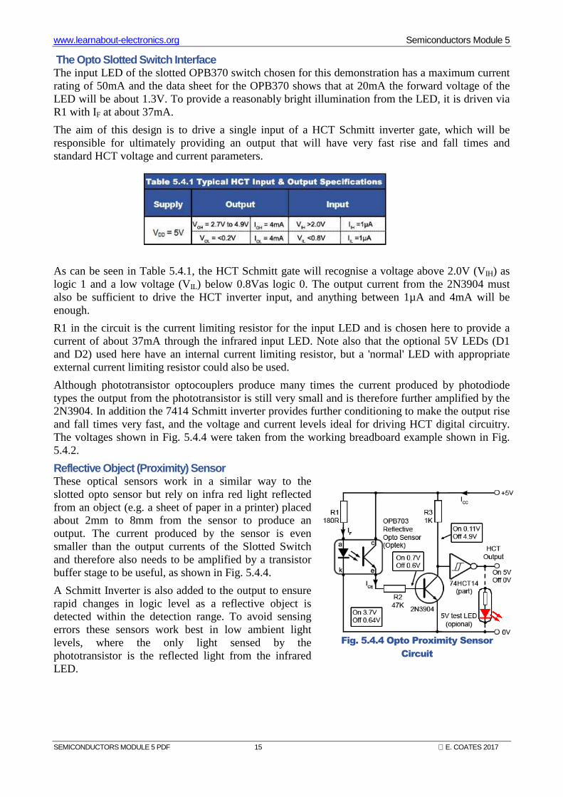
The Opto Slotted Switch Interface The input LED of the slotted OPB370 switch chosen for this demonstration has a maximum current rating of 50mA and the data sheet for the OPB370 shows that at 20mA the forward voltage of the LED will be about 1.3V. To provide a reasonably bright illumination from the LED, it is driven via R1 with IF at about 37mA.
The aim of this design is to drive a single input of a HCT Schmitt inverter gate, which will be responsible for ultimately providing an output that will have very fast rise and fall times and standard HCT voltage and current parameters.
As can be seen in Table 5.4.1, the HCT Schmitt gate will recognise a voltage above 2.0V (VIH) as logic 1 and a low voltage (VIL) below 0.8Vas logic 0. The output current from the 2N3904 must also be sufficient to drive the HCT inverter input, and anything between 1µA and 4mA will be enough.
R1 in the circuit is the current limiting resistor for the input LED and is chosen here to provide a current of about 37mA through the infrared input LED. Note also that the optional 5V LEDs (D1 and D2) used here have an internal current limiting resistor, but a 'normal' LED with appropriate external current limiting resistor could also be used.
Although phototransistor optocouplers produce many times the current produced by photodiode types the output from the phototransistor is still very small and is therefore further amplified by the 2N3904. In addition the 7414 Schmitt inverter provides further conditioning to make the output rise and fall times very fast, and the voltage and current levels ideal for driving HCT digital circuitry. The voltages shown in Fig. 5.4.4 were taken from the working breadboard example shown in Fig. 5.4.2.
Reflective Object (Proximity) Sensor These optical sensors work in a similar way to the slotted opto sensor but rely on infra red light reflected from an object (e.g. a sheet of paper in a printer) placed about 2mm to 8mm from the sensor to produce an output. The current produced by the sensor is even smaller than the output currents of the Slotted Switch and therefore also needs to be amplified by a transistor buffer stage to be useful, as shown in Fig. 5.4.4.
A Schmitt Inverter is also added to the output to ensure rapid changes in logic level as a reflective object is detected within the detection range. To avoid sensing errors these sensors work best in low ambient light levels, where the only light sensed by the phototransistor is the reflected light from the infrared LED.
Fig. 5.4.4 Opto Proximity Sensor
Circuit
www.learnabout-electronics.org Semiconductors Module 5
SEMICONDUCTORS MODULE 5 PDF 16 E. COATES 2017
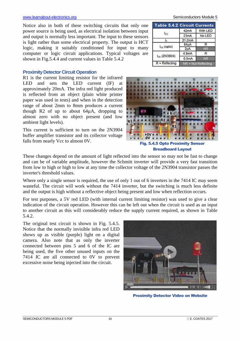
Notice also in both of these switching circuits that only one power source is being used, as electrical isolation between input and output is normally less important. The input to these sensors is light rather than some electrical property. The output is HCT logic, making it suitably conditioned for input to many computer or logic circuit applications. Typical voltages are shown in Fig.5.4.4 and current values in Table 5.4.2
Proximity Detector Circuit Operation R1 is the current limiting resistor for the infrared LED and sets the LED current (IF) at approximately 20mA. The infra red light produced is reflected from an object (plain white printer paper was used in tests) and when in the detection range of about 2mm to 8mm produces a current though R2 of up to about 64µA, dropping to almost zero with no object present (and low ambient light levels).
This current is sufficient to turn on the 2N3904 buffer amplifier transistor and its collector voltage falls from nearly Vcc to almost 0V.
These changes depend on the amount of light reflected into the sensor so may not be fast to change and can be of variable amplitude, however the Schmitt inverter will provide a very fast transition from low to high or high to low at any time the collector voltage of the 2N3904 transistor passes the inverter's threshold values.
Where only a single sensor is required, the use of only 1 out of 6 inverters in the 7414 IC may seem wasteful. The circuit will work without the 7414 inverter, but the switching is much less definite and the output is high without a reflective object being present and low when reflection occurs.
For test purposes, a 5V red LED (with internal current limiting resistor) was used to give a clear indication of the circuit operation. However this can be left out when the circuit is used as an input to another circuit as this will considerably reduce the supply current required, as shown in Table 5.4.2.
The original test circuit is shown in Fig. 5.4.5. Notice that the normally invisible infra red LED shows up as visible (purple) light on a digital camera. Also note that as only the inverter connected between pins 5 and 6 of the IC are being used, the five other unused inputs on the 7414 IC are all connected to 0V to prevent excessive noise being injected into the circuit.
Fig. 5.4.5 Opto Proximity Sensor
Breadboard Layout
Proximity Detector Video on Website
www.learnabout-electronics.org Semiconductors Module 5
SEMICONDUCTORS MODULE 5 PDF 17 E. COATES 2017
Module 5.5 Optocoupler Quiz Try this quiz based on optocouplers. Hopefully it'll be easy. Submit your answers but don't be disappointed if you get answers wrong. All the information you need is on this website. Find the right answer and learn about transistors as you go.
1.
What type of optocoupler output is illustrated Fig. 5.5.1?
a) Phototransistor.
b) Photodiode.
c) Phototriac.
d) PhotoSCR
2.
A phototransistor produces more current than a photodiode because - (Choose an answer to complete this sentence)
a) - the phototransistor can be more heavily doped than the photodiode.
b) - the photo transistor accepts a wider spectrum of light than the photodiode.
c) - the current produced by photons is amplified by the hfe of the transistor.
d) - the photodiode is normally used in low light conditions.
3.
Which of the following operation modes do photo proximity detectors normally use?
a) Linear Mode.
b) Saturation Mode.
c) Analogue Mode.
d) Direct Mode.
4.
Fig. 5.5.2 illustrates an IL300 audio optocoupler, which uses one infrared LED and two photodiodes. What is the usual purpose of the second photodiode?
a) To double the output voltage when connecting the two diodes in parallel.
b) To provide back emf protection.
c) To provide compensation for variations in CTR.
d) To generate a DC bias from an AC signal.
5.
An optocoupler having a maximum input current (IF) of 50mA is chosen to be driven by a current of 20mA. Which of the following answers would be a valid reason for this?
a) To allow for input surge currents.
b) To reduce input noise.
c) To allow for LED ageing.
d) To allow for the occurrence of voltage spikes at the input.
www.learnabout-electronics.org Semiconductors Module 5
SEMICONDUCTORS MODULE 5 PDF 18 E. COATES 2017
6.
Which of the formulae in Fig.5.5.3 correctly describes the CTR of an optocoupler?
a) Formula a
b) Formula b
c) Formula c
d) Formula d
7.
What is the purpose of RV1 in the audio optocoupler circuit shown in Fig 5.5.4?
a) To adjust for maximum current ICE.
b) To adjust for minimum DC bias voltage.
c) To adjust for maximum volume.
d) To adjust for minimum distortion.
8.
Refer to Fig. 5.5.5. What will be the approximate 'On' and 'Off' voltages at the collector of the 2N3904 transistor?
a) On = 2.0V Off = 0.8V
b) On = 0.1V Off = 4.9V
c) On = 5.0V Off = 0.2V
d) On = 4.5V Off = 0.3V
9.
Compared to a photo-diode,which of the listed advantages and disadvantages would be expected of a photo-transistor
a) Faster response and greater sensitivity.
b) Faster response and less sensitivity.
c) Slower response and greater sensitivity.
d) Slower response and less sensitivity.
Continued
www.learnabout-electronics.org Semiconductors Module 5
SEMICONDUCTORS MODULE 5 PDF 19 E. COATES 2017
10.
Refer to Fig. 5.5.6. With the input and output signals shown, what level of signal voltage would you expect at point A?
a) 0Vpp to 0.1Vpp
b) 0.1Vpp to 1Vpp
c) 1Vpp to 10Vpp
d) 10Vpp to 20Vpp