
Optimization of Space Vector Pulse Width Modulation .... Basic. Appl. Sci. Res., 2(8...Optimization...
13
J. Basic. Appl. Sci. Res., 2(8)7632-7644, 2012 © 2012, TextRoad Publication ISSN 2090-4304 Journal of Basic and Applied Scientific Research www.textroad.com *Corresponding Author: Mohamad Reza Alizadeh Pahlavani, Islamic Azad University of Iran, Boroujerd Branch Optimization of Space Vector Pulse Width Modulation Switching Algorithms for Two-Level Inverters Regarding Different Objective Functions Mohamad Reza Alizadeh Pahlavani 1 , Yousef Khadivi Vaneqi 2 1,2 Islamic Azad University of Iran, Boroujerd Branch ABSTRACT Inverters are able to produce single or three phase AC voltages from a constant or variable DC voltage. There are several algorithms to control output voltage. In addition to the desired output harmonic, each algorithm produces unwanted harmonics at Voltage Source Inverter (VSI) output voltage. In case of reducing low order harmonics, Space Vector Pulse Width Modulation (SVPWM) is more effective than other PWM algorithms such as trapezoidal, sinusoidal, harmonic injected, delta and phase shifted PWM. One may use different strategies to implement SVPWM algorithm in case of sector utilization in each switching period. Different strategies may be of relative advantages and disadvantages with respect to each other. In this paper, we propose five different strategies to synthesize the same output voltage using SVPWM. Then, we will introduce the best algorithm, with respect to different indices such as Total Harmonic Distortion (THD), Distortion Factor (DF), conduction loss, switching loss and the ratio of the main harmonic to other harmonic components. It is also shown that by selecting an optimized and appropriate Switching State (SS) for SVPWM, the harmonic orders, which are the multiples of the frequency index (FI), are eliminated. Then, to investigate the impact of variations of the capacitor’s voltage and switching frequency on power quality criteria, the most appropriate and optimized SS is applied to a 3P three-level (3L) Neutral-Point-Clamped (NPC) VSI to supply a 3P load. At the end, we will show experimental results of the implemented laboratory prototype on a three phase load to demonstrate validity of our simulations and control algorithm. KEYWORDS: two level inverter, conduction loss, switching loss, harmonic distortion index, space vector pulse width modulation. 1- INTRODUCTION A Voltage Source Inverter converts input DC voltage to an AC voltage with desired amplitude and frequency. Capability of changing output frequency and amplitude with low distortion is one of the main characteristics of a good inverter. Variable output voltage is obtained by changing input DC voltage or inverter gain (ratio of output AC voltage amplitude to input DC). In general, inverter gain is changed by PWM technique. Among many different PWM techniques, SVPWM is more effective in terms of reducing harmonic distortion of output voltage. Since electrical ratings of power electronic devices are limited, utilization of multilevel structures to implement high power inverters is inevitable. The multi-level converter is an interface between the power network and the capacitor bank and controls the electrical energy exchange between them. In addition to obtain high powers in electronic converters, some of other advantages of multi-level topologies are reduction of voltage on each switch, decreasing or eliminating lateral equipment, decreasing switching frequency, decreasing THD, decreasing switching losses, and decreasing the output current ripple. Multi-level converters, on the other hand, have some disadvantages associated with their use, some of which are increase in complexity of the control systems, the number of power electronic devices, and the asymmetry of the capacitor voltages during charge and discharge [17-21]. However, the trend toward increasing the speed of electronic processors and the steady decrease in the cost of power electronic devices, coupled with the ability to implement advanced modulation methods such as the SVPWM, encourage engineers to ignore the disadvantages of multi-level converters [22-25]. NPC is one of several multi-level structures that we have used in this paper. The structure of this paper is as follows: In Section 2, the principle of space vector pulse width modulation is presented. Also, the SSs of SVPWM are presented and studied. In Section 3, we will introduce our proposed SVPWM techniques. In section 4, we will simulate and discuss about behavior of the most appropriate and optimized SS from other strategies. In Section 5, we will show experimental results of our work and compare it with our simulations. These results will validate our ideas and simulations. 7632
Transcript of Optimization of Space Vector Pulse Width Modulation .... Basic. Appl. Sci. Res., 2(8...Optimization...

J. Basic. Appl. Sci. Res., 2(8)7632-7644, 2012
© 2012, TextRoad Publication
ISSN 2090-4304 Journal of Basic and Applied
Scientific Research www.textroad.com
*Corresponding Author: Mohamad Reza Alizadeh Pahlavani, Islamic Azad University of Iran, Boroujerd Branch
Optimization of Space Vector Pulse Width Modulation Switching Algorithms for Two-Level Inverters Regarding Different Objective Functions
Mohamad Reza Alizadeh Pahlavani1, Yousef Khadivi Vaneqi2
1,2Islamic Azad University of Iran, Boroujerd Branch
ABSTRACT
Inverters are able to produce single or three phase AC voltages from a constant or variable DC voltage. There are several algorithms to control output voltage. In addition to the desired output harmonic, each algorithm produces unwanted harmonics at Voltage Source Inverter (VSI) output voltage. In case of reducing low order harmonics, Space Vector Pulse Width Modulation (SVPWM) is more effective than other PWM algorithms such as trapezoidal, sinusoidal, harmonic injected, delta and phase shifted PWM. One may use different strategies to implement SVPWM algorithm in case of sector utilization in each switching period. Different strategies may be of relative advantages and disadvantages with respect to each other. In this paper, we propose five different strategies to synthesize the same output voltage using SVPWM. Then, we will introduce the best algorithm, with respect to different indices such as Total Harmonic Distortion (THD), Distortion Factor (DF), conduction loss, switching loss and the ratio of the main harmonic to other harmonic components. It is also shown that by selecting an optimized and appropriate Switching State (SS) for SVPWM, the harmonic orders, which are the multiples of the frequency index (FI), are eliminated. Then, to investigate the impact of variations of the capacitor’s voltage and switching frequency on power quality criteria, the most appropriate and optimized SS is applied to a 3P three-level (3L) Neutral-Point-Clamped (NPC) VSI to supply a 3P load. At the end, we will show experimental results of the implemented laboratory prototype on a three phase load to demonstrate validity of our simulations and control algorithm. KEYWORDS: two level inverter, conduction loss, switching loss, harmonic distortion index, space vector pulse width modulation.
1- INTRODUCTION
A Voltage Source Inverter converts input DC voltage to an AC voltage with desired amplitude and frequency.
Capability of changing output frequency and amplitude with low distortion is one of the main characteristics of a good inverter. Variable output voltage is obtained by changing input DC voltage or inverter gain (ratio of output AC voltage amplitude to input DC). In general, inverter gain is changed by PWM technique. Among many different PWM techniques, SVPWM is more effective in terms of reducing harmonic distortion of output voltage.
Since electrical ratings of power electronic devices are limited, utilization of multilevel structures to implement high power inverters is inevitable. The multi-level converter is an interface between the power network and the capacitor bank and controls the electrical energy exchange between them. In addition to obtain high powers in electronic converters, some of other advantages of multi-level topologies are reduction of voltage on each switch, decreasing or eliminating lateral equipment, decreasing switching frequency, decreasing THD, decreasing switching losses, and decreasing the output current ripple. Multi-level converters, on the other hand, have some disadvantages associated with their use, some of which are increase in complexity of the control systems, the number of power electronic devices, and the asymmetry of the capacitor voltages during charge and discharge [17-21]. However, the trend toward increasing the speed of electronic processors and the steady decrease in the cost of power electronic devices, coupled with the ability to implement advanced modulation methods such as the SVPWM, encourage engineers to ignore the disadvantages of multi-level converters [22-25]. NPC is one of several multi-level structures that we have used in this paper.
The structure of this paper is as follows: In Section 2, the principle of space vector pulse width modulation is presented. Also, the SSs of SVPWM are presented and studied. In Section 3, we will introduce our proposed SVPWM techniques. In section 4, we will simulate and discuss about behavior of the most appropriate and optimized SS from other strategies. In Section 5, we will show experimental results of our work and compare it with our simulations. These results will validate our ideas and simulations.
7632
Pahlavani and Vaneqi, 2012
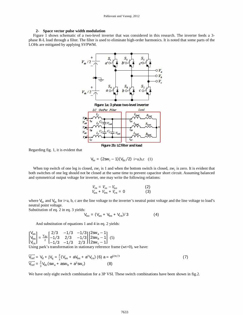
2- Space vector pulse width modulation Figure 1 shows schematic of a two-level inverter that was considered in this research. The inverter feeds a 3-
phase R-L load through a filter. The filter is used to eliminate high-order harmonics. It is noted that some parts of the LOHs are mitigated by applying SVPWM.
Figure 1a: 3 phase two-level inverter
Figure 2b: LC filter and load
Regarding fig. 1, it is evident that
V = (2sw − 1)(V 2⁄ ) i=a,b,c (1)
When top switch of one leg is closed, 푠푤 is 1 and when the bottom switch is closed, 푠푤 is zero. It is evident that both switches of one leg should not be closed at the same time to prevent capacitor short circuit. Assuming balanced and symmetrical output voltage for inverter, one may write the following relations:
푉 = 푉 − 푉 (2) 푉 + 푉 + 푉 = 0 (3)
where V and V for i=a, b, c are the line voltage to the inverter’s neutral point voltage and the line voltage to load’s neutral point voltage. Substitution of eq. 2 in eq. 3 yields:
V = (V + V + V )/3 (4)
And substitution of equations 1 and 4 in eq. 2 yields:
VVV
=2 3⁄ −1 3⁄ −1 3⁄−1 3⁄ 2 3⁄ −1 3⁄−1 3⁄ −1 3⁄ 2 3⁄
2sw − 12sw − 12sw − 1
(5)
Using park’s transformation in stationary reference frame (wt=0), we have: V = V + jV = (V + aV + a V ) (6) a = e ⁄ (7) V = V (sw + asw + a sw ) (8) We have only eight switch combination for a 3P VSI. These switch combinations have been shown in fig.2.
7633
J. Basic. Appl. Sci. Res., 2(8)7632-7644, 2012
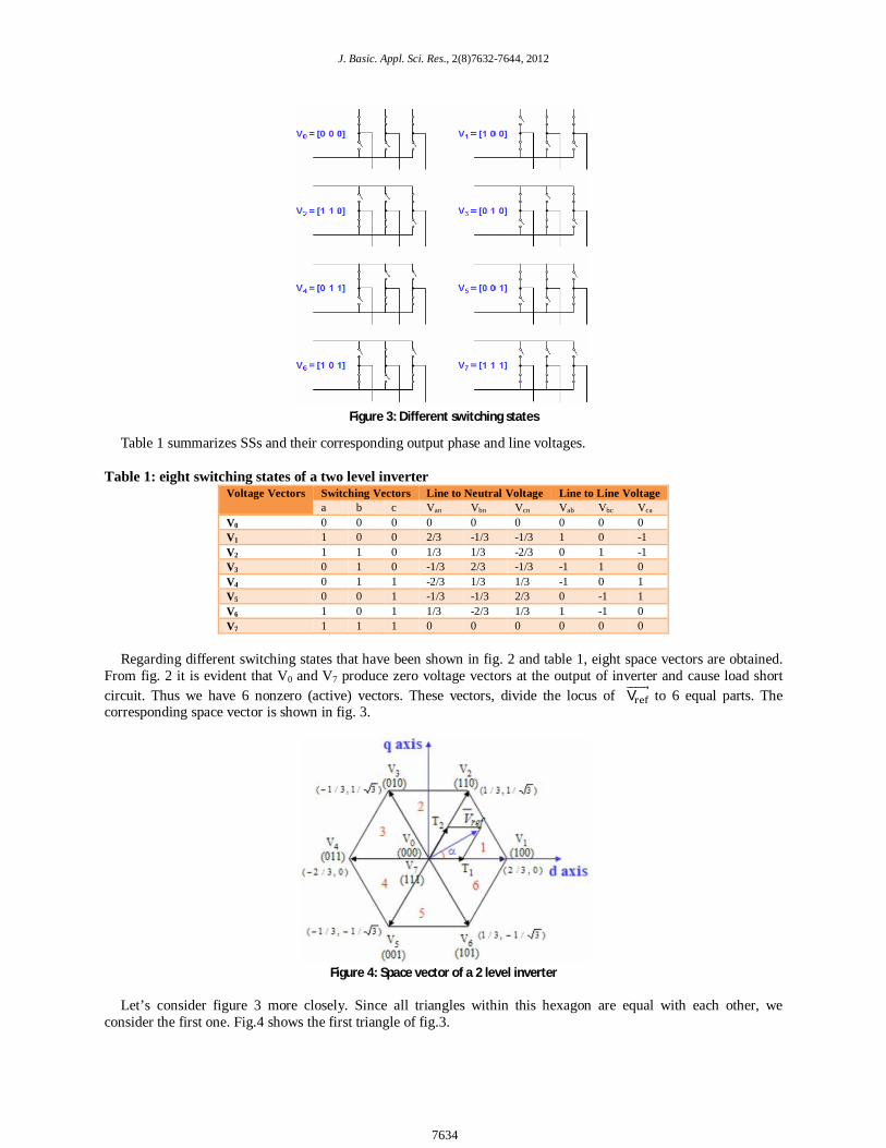
Figure 3: Different switching states
Table 1 summarizes SSs and their corresponding output phase and line voltages.
Table 1: eight switching states of a two level inverter Voltage Vectors Switching Vectors Line to Neutral Voltage Line to Line Voltage
a b c Van Vbn Vcn Vab Vbc Vca
V0 0 0 0 0 0 0 0 0 0 V1 1 0 0 2/3 -1/3 -1/3 1 0 -1 V2 1 1 0 1/3 1/3 -2/3 0 1 -1 V3 0 1 0 -1/3 2/3 -1/3 -1 1 0 V4 0 1 1 -2/3 1/3 1/3 -1 0 1 V5 0 0 1 -1/3 -1/3 2/3 0 -1 1 V6 1 0 1 1/3 -2/3 1/3 1 -1 0 V7 1 1 1 0 0 0 0 0 0
Regarding different switching states that have been shown in fig. 2 and table 1, eight space vectors are obtained.
From fig. 2 it is evident that V0 and V7 produce zero voltage vectors at the output of inverter and cause load short circuit. Thus we have 6 nonzero (active) vectors. These vectors, divide the locus of V to 6 equal parts. The corresponding space vector is shown in fig. 3.
Figure 4: Space vector of a 2 level inverter
Let’s consider figure 3 more closely. Since all triangles within this hexagon are equal with each other, we
consider the first one. Fig.4 shows the first triangle of fig.3.
7634
Pahlavani and Vaneqi, 2012
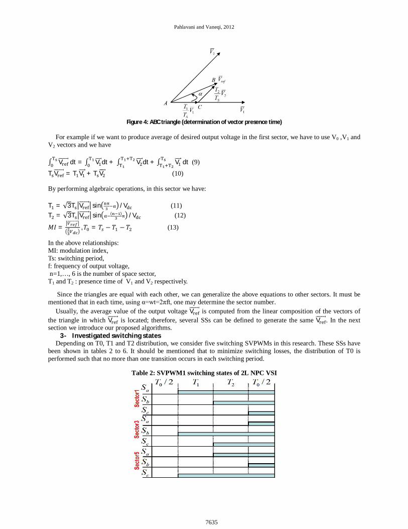
Figure 4: ABC triangle (determination of vector presence time)
For example if we want to produce average of desired output voltage in the first sector, we have to use V0 ,V1 and
V2 vectors and we have
∫ V dt = ∫ Vdt + ∫ Vdt + ∫ V dt (9)
T V = T V+ T V (10) By performing algebraic operations, in this sector we have:
T = √3T V sin /V (11) T = √3T V sin ( ) /V (12)
푀퐼 =
,푇 = 푇 − 푇 − 푇 (13)
In the above relationships: MI: modulation index, Ts: switching period, f: frequency of output voltage, n=1,…, 6 is the number of space sector, T1 and T2 : presence time of V1 and V2 respectively.
Since the triangles are equal with each other, we can generalize the above equations to other sectors. It must be
mentioned that in each time, using α=wt=2πft, one may determine the sector number. Usually, the average value of the output voltage V is computed from the linear composition of the vectors of
the triangle in which V is located; therefore, several SSs can be defined to generate the same V . In the next section we introduce our proposed algorithms.
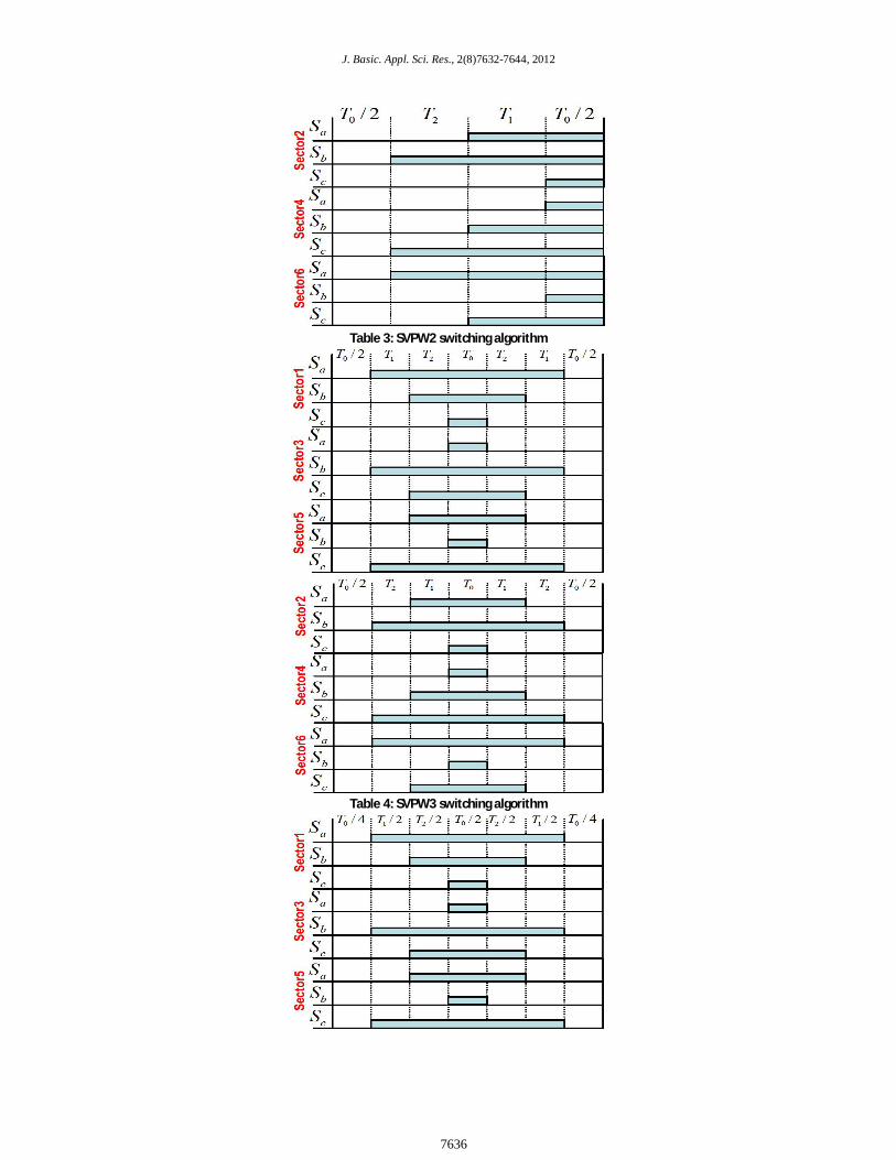
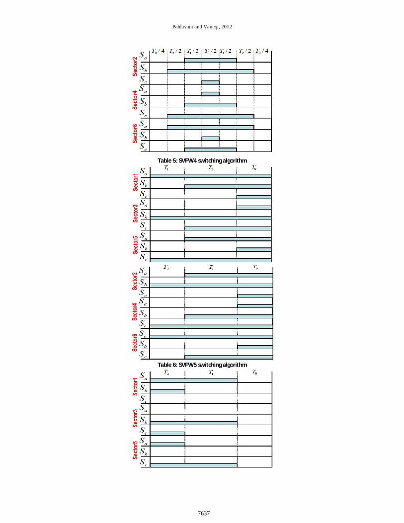
3- Investigated switching states Depending on T0, T1 and T2 distribution, we consider five switching SVPWMs in this research. These SSs have
been shown in tables 2 to 6. It should be mentioned that to minimize switching losses, the distribution of T0 is performed such that no more than one transition occurs in each switching period.
Table 2: SVPWM1 switching states of 2L NPC VSI
7635
J. Basic. Appl. Sci. Res., 2(8)7632-7644, 2012
Table 3: SVPW2 switching algorithm
Table 4: SVPW3 switching algorithm
7636
Pahlavani and Vaneqi, 2012
Table 5: SVPW4 switching algorithm
Table 6: SVPW5 switching algorithm
7637
J. Basic. Appl. Sci. Res., 2(8)7632-7644, 2012
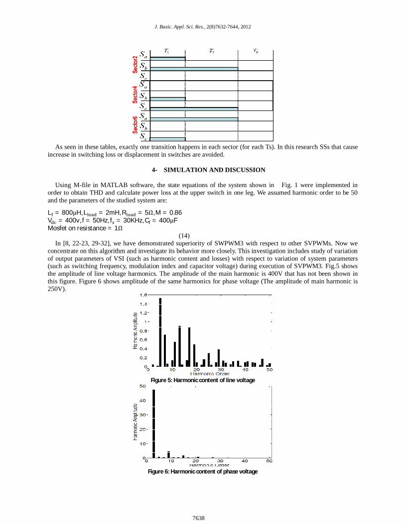
As seen in these tables, exactly one transition happens in each sector (for each Ts). In this research SSs that cause
increase in switching loss or displacement in switches are avoided.
4- SIMULATION AND DISCUSSION Using M-file in MATLAB software, the state equations of the system shown in Fig. 1 were implemented in
order to obtain THD and calculate power loss at the upper switch in one leg. We assumed harmonic order to be 50 and the parameters of the studied system are:
L = 800μH, L = 2mH, R = 5Ω, M = 0.86 V = 400v, f = 50Hz, f = 30KHz, C = 400μF Mosfet on resistance = 1Ω
(14) In [8, 22-23, 29-32], we have demonstrated superiority of SWPWM3 with respect to other SVPWMs. Now we
concentrate on this algorithm and investigate its behavior more closely. This investigation includes study of variation of output parameters of VSI (such as harmonic content and losses) with respect to variation of system parameters (such as switching frequency, modulation index and capacitor voltage) during execution of SVPWM3. Fig.5 shows the amplitude of line voltage harmonics. The amplitude of the main harmonic is 400V that has not been shown in this figure. Figure 6 shows amplitude of the same harmonics for phase voltage (The amplitude of main harmonic is 250V).
Figure 5: Harmonic content of line voltage
Figure 6: Harmonic content of phase voltage
7638
Pahlavani and Vaneqi, 2012
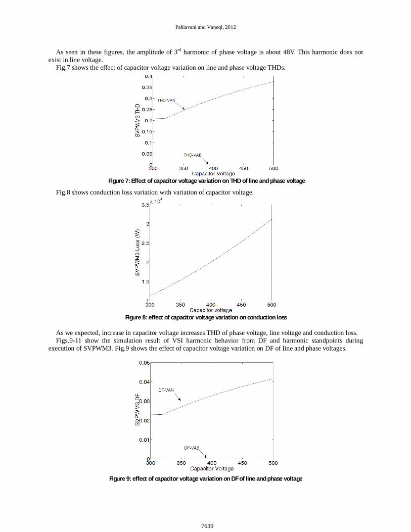
As seen in these figures, the amplitude of 3rd harmonic of phase voltage is about 48V. This harmonic does not exist in line voltage.
Fig.7 shows the effect of capacitor voltage variation on line and phase voltage THDs.
Figure 7: Effect of capacitor voltage variation on THD of line and phase voltage
Fig.8 shows conduction loss variation with variation of capacitor voltage.
Figure 8: effect of capacitor voltage variation on conduction loss
As we expected, increase in capacitor voltage increases THD of phase voltage, line voltage and conduction loss. Figs.9-11 show the simulation result of VSI harmonic behavior from DF and harmonic standpoints during
execution of SVPWM3. Fig.9 shows the effect of capacitor voltage variation on DF of line and phase voltages.
Figure 9: effect of capacitor voltage variation on DF of line and phase voltage
7639
J. Basic. Appl. Sci. Res., 2(8)7632-7644, 2012
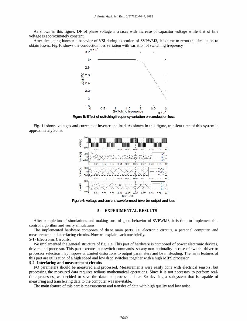
As shown in this figure, DF of phase voltage increases with increase of capacitor voltage while that of line voltage is approximately constant.
After simulating harmonic behavior of VSI during execution of SVPWM3, it is time to rerun the simulation to obtain losses. Fig.10 shows the conduction loss variation with variation of switching frequency.
Figure 5: Effect of switching frequency variation on conduction loss.
Fig. 11 shows voltages and currents of inverter and load. As shown in this figure, transient time of this system is
approximately 30ms.
Figure 6: voltage and current waveforms of inverter output and load
5- EXPERIMENTAL RESULTS
After completion of simulations and making sure of good behavior of SVPWM3, it is time to implement this
control algorithm and verify simulations. The implemented hardware composes of three main parts, i.e. electronic circuits, a personal computer, and
measurement and interfacing circuits. Now we explain each one briefly. 5-1- Electronic Circuits:
We implemented the general structure of fig. 1.a. This part of hardware is composed of power electronic devices, drivers and processor. This part executes our switch commands, so any non-optimality in case of switch, driver or processor selection may impose unwanted distortions to output parameters and be misleading. The main features of this part are utilization of a high speed and low drop switches together with a high MIPS processor. 5-2- Interfacing and measurement circuits
I/O parameters should be measured and processed. Measurements were easily done with electrical sensors; but processing the measured data requires tedious mathematical operations. Since it is not necessary to perform real-time processes, we decided to save the data and process it later. So devising a subsystem that is capable of measuring and transferring data to the computer was inevitable.
The main feature of this part is measurement and transfer of data with high quality and low noise.
7640
Pahlavani and Vaneqi, 2012
5-3- Computer and software As mentioned earlier, the data was measured and saved in computer. The raw data should be processed and the
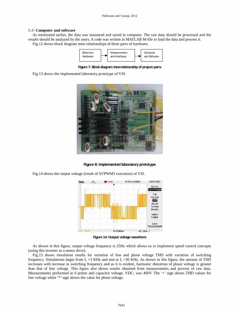
results should be analyzed by the users. A code was written in MATLAB M-file to load the data and process it. Fig.12 shows block diagram inter-relationships of three parts of hardware.
Figure 7: Block diagram interrelationship of project parts
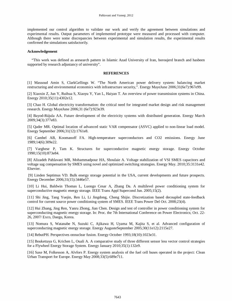
Fig.13 shows the implemented laboratory prototype of VSI.
Figure 8: Implemented laboratory prototype
Fig.14 shows the output voltage (result of SVPWM3 execution) of VSI.
Figure 14: Output voltage waveform As shown in this figure, output voltage frequency is 25Hz which allows us to implement speed control concepts
(using this inverter as a motor drive). Fig.15 shows simulation results for variation of line and phase voltage THD with variation of switching
frequency. Simulations begin from fs =3 KHz and end at fs =30 KHz. As shown in this figure, the amount of THD increases with increase in switching frequency and as it is evident, harmonic distortion of phase voltage is greater than that of line voltage. This figure also shows results obtained from measurements and process of raw data. Measurements performed in 6 points and capacitor voltage, VDC; was 400V. The ‘+’ sign shows THD values for line voltage while ‘*’ sign shows the value for phase voltage.
Electronic Hardware
Measurements and Interfaces
Computer and Software
7641

J. Basic. Appl. Sci. Res., 2(8)7632-7644, 2012
Figure15: Effect of switching frequency variation on THD of line and phase voltages
Fig.16 shows simulation and experimental results for DF of line and phase voltages together. This figure shows
the effect of switching frequency variation on DF of phase and line voltages. As shown in this figure, distortion factor of line voltage is approximately constant while for phase voltage it increases as fs increases.
Figure 16: Effect of switching frequency variation on DF of phase and line voltages.
As shown in figures 17 and 18, experimental values have small discrepancies with simulations, but their sequence
and differences (with each other) are the same as simulations. In case of losses, since it is not possible to directly measure the switching losses, we calculate the efficiencies of
the circuit during execution of SVPWM1-5. Table 7 shows the values of efficiencies during execution of each SVPWM.
Table 7: SVPWM1-5 efficiencies scheme SVPWM1 SVPWM2 SVPWM3 SVPWM4 SVPWM5 Efficiency 0.85 0.9 0.85 0.87 0.87
Since total losses (excluding switching losses) of the circuit are constant, we may use the efficiencies as an index
of switching loss. So a lower efficiency is equivalent to higher switching loss. As seen in table 9, the exact value of loss (efficiency) does not exactly correspond to simulations (this is caused by physical phenomenon of electrical components that could not be exactly simulated) but as it seems, the sequence and quality of efficiencies conforms to simulations. One may reduce switching loss by utilization of soft switching techniques, so this parameter has lower weight with respect to harmonic behavior of each switching algorithm.
6- Conclusion
To increase the quality of multilevel inverter utilization, optimization of switching strategies of SVPWM is
inevitable. SVPWM3 was chosen as the best due to its good behavior from harmonic and loss standpoints. We
7642
Pahlavani and Vaneqi, 2012
implemented our control algorithm to validate our work and verify the agreement between simulations and experimental results. Output parameters of implemented prototype were measured and processed with computer. Although there were some discrepancies between experimental and simulation results, the experimental results confirmed the simulations satisfactorily.
Acknowledgement
“This work was defined as aresearch pattern in Islamic Azad University of Iran, boroujerd branch and hasbeen
supported by research adjustancy of university”.
REFERENCES [1] Massoud Amin S, ClarkGellings W. “The North American power delivery system: balancing market restructuring and environmental economics with infrastructure security,”. Energy MayeJune 2006;31(6e7):967e99.
[2] Xiaoxin Z, Jun Y, Ruihua S, Xiaoyu Y, Yan L, Haiyan T. An overview of power transmission systems in China. Energy 2010;35(11):4302e12.
[3] Chao H. Global electricity transformation: the critical need for integrated market design and risk management research. Energy MayeJune 2006;31 (6e7):923e39.
[4] Bayod-Rújula AA. Future development of the electricity systems with distributed generation. Energy March 2009;34(3):377e83.
[5] Qader MR. Optimal location of advanced static VAR compensator (ASVC) applied to non-linear load model. Energy September 2006;31(12):1761e8.
[6] Cambel AB, Koomanoff FA. High-temperature superconductors and CO2 emissions. Energy June 1989;14(6):309e22.
[7] Varghese P, Tam K. Structures for superconductive magnetic energy storage. Energy October 1990;15(10):873e84.
[8] Alizadeh Pahlavani MR, Mohammadpour HA, Shoulaie A. Voltage stabilization of VSI SMES capacitors and voltage sag compensation by SMES using novel and optimized switching strategies. Energy May. 2010;35:3131e42. Elsevier.
[9] Linden Septimus VD. Bulk energy storage potential in the USA, current developments and future prospects. Energy December 2006;31(15):3446e57.
[10] Li Hui, Baldwin Thomas L, Luongo Cesar A, Zhang Da. A multilevel power conditioning system for superconductive magnetic energy storage. IEEE Trans Appl Supercond Jun. 2005;15(2).
[11] Shi Jing, Tang Yuejin, Ren Li, Li Jingdong, Cheng Shijie. Discretization based decoupled state-feedback control for current source power conditioning system of SMES. IEEE Trans Power Del Oct. 2008;23(4).
[12] Hui Zhang, Jing Ren, Yanru Zhong, Jian Chen. Design and test of controller in power conditioning system for superconducting magnetic energy storage. In: Proc. the 7th International Conference on Power Electronics; Oct. 22-26, 2007/ Exco, Daegu, Korea.
[13] Nomura S, Watanabe N, Suzuki C, Ajikawa H, Uyama M, Kajita S, et al. Advanced configuration of superconducting magnetic energy storage. Energy AugusteSeptember 2005;30(11e12):2115e27.
[14] RebutPH. Perspectives onnuclear fusion. Energy October 1993;18(10):1023e31.
[15] Boukettaya G, Krichen L, Ouali A. A comparative study of three different sensor less vector control strategies for a Flywheel Energy Storage System. Energy January 2010;35(1):132e9.
[16] Saxe M, Folkesson A, Alvfors P. Energy system analysis of the fuel cell buses operated in the project: Clean Urban Transport for Europe. Energy May 2008;33(5):689e711.
7643
J. Basic. Appl. Sci. Res., 2(8)7632-7644, 2012
[17] Purkait P, Sriramakavacham RS. A new generalized space vector modulation algorithm for neutral point clamped multi-level converters. In: Progress in Electromagnetic Research Symposium, Cambridge, USA; Mar 2006, p. 26e29.
[18] Franquelo LG. Simple and advanced three dimensional space vector modulation algorithm for four-leg multi-level converters topology. In: 30th Annual Conference of the IEEE Industrial Electronics Society, Busan, Korea; Nov 2004. p. 2e6.
[19] Zhou K, Wang D. Relationship between space vector modulation and threephase carrier-based PWM A comprehensive analysis. IEEE Trans Ind Electron Feb. 2002;49(1).
[20] delos M, Prats AM. New space vector modulation algorithms. HAIT J Sci Eng B 2005;2(5e6):690e714.
[21] Kwasinski A. Time domain comparison of pulse-width modulation schemes. IEEE Power Electron Lett Sep. 2003;1(3).
[22] Alizadeh Pahlavani MR,Shoulaie A. Comparison of space vector pulse width modulation switching patterns in three level VSI to approach power quality factors. In: Proc. 23rd International Power System Conf, Tehran, Iran; Nov. 2008 [in Persian].
[23] Alizadeh Pahlavani MR, Shoulaie A. Switching pattern optimization of space vector pulse width modulation in two level VSIs with different objective functions. In: Proc. 22nd International Power System Conf, Tehran, Iran; October. 2007 [in Persian].
[24] Gupta Amit Kumar, Khambadkone Ashwin M. A space vector PWM scheme for multilevel VSIs based on two-level space vector PWM. IEEE Trans Ind Electron Oct. 2006;53(5).
[25] Gupta Amit Kumar, Khambadkone Ashwin M. A simple space vector PWM scheme to operate a three-level NPC VSI at high modulation index including overmodulation region, with neutral point balancing. IEEE Trans Ind Appl May/June 2007;43(3).
[26] Mao H, Boroyevich D, Lee FC. Multi-level 2-quadrant boost choppers for superconducting magnetic energy storage. Conf IEEE; 1996.
[27] Alizadeh Pahlavani MR, Shoulaie A. Comparing space vector pulse width modulation switching strategies in over modulation state. In: Proc. 18th Iranian Conference on Electrical Engineering, Isfahan, Iran, 2010 [in Persian].
[28] Alizadeh Pahlavani MR, Mohammadpour HA, Shoulaie A. A novel scheme for chopper switching to control three level VSI capacitor voltage. In: 17th Iranian Conference on Electrical Engineering (ICEE), Tehran, Iran, IUST; 2009 [in Persian].
[29]M. R. Alizadeh Pahlavani, H. A. Mohammadpour, “An Optimized SVPWM Switching Strategy for Three-Level NPC VSI and A Novel Switching Strategy for Three-Level Two-Quadrant Chopper to Stabilize the Voltage of Capacitors,” Elsevier, Energy, 35, pp. 4917-4931, Oct. 2010.
[30] M. R. Alizadeh Pahlavani, M. A. Bassam, “Voltage Stabilization of SMES VSI DC-Link and Compensation of Reactive Power by SMES Using Optimized Switching Strategies,” International Journal of Power and Energy Conversion, Accepted to be published, 2011.
[31]M. R. Alizadeh Pahlavani, H. A. Mohammadpour, A. Shoulaie, “Voltage stabilization of VSI SMES capacitors and voltage sag compensation by SMES using novel and optimized switching strategies, ” in Proc. 24th International Power System Conf, Tehran, Iran, no. 09-E-PQA-0110, Nov. 2009.
[32]M. R. Alizadeh Pahlavani, A. Shoulaie, “Comparing Space Vector Pulse Width Modulation Switching Strategies in over Modulation State,” in Proc. 18th Iranian Conference on Electrical Engineering, Isfahan, Iran, pp. 1932-1937, May. 2010, Persian.
7644