Optimization of a scintillation detector with wave length ... · average energy loss per unit path...
120
Optimization of a scintillation detector with wave length shifting fiber and SiPM readout Optimierung eines Szintillationsdetektors mit wellenlängenschiebender Faser und SiPM-Auslese Masterarbeit der Fakultät für Physik der Ludwig-Maximilians-Universität München vorgelegt von Johannes Großmann geboren in Lichtenfels München, den 30.10.2014
Transcript of Optimization of a scintillation detector with wave length ... · average energy loss per unit path...

Optimization of a scintillation detector with wave
length shifting fiber and SiPM readout
Optimierung eines Szintillationsdetektors mit
wellenlängenschiebender Faser und SiPM-Auslese
Masterarbeit der Fakultät für Physik
der
Ludwig-Maximilians-Universität München
vorgelegt von
Johannes Großmann
geboren in Lichtenfels
München, den 30.10.2014

Gutachter: Prof. Dr. Otmar Biebel


Abstract
The Cosmic Ray Facility (CRF) in Garching detects cosmic muons with a precision of50 µm. It will be used for commissioning and calibration of micromegas detectors,which will be part of the ATLAS new small wheel upgrade. The current energyselector consists of an iron absorber, a trigger hodoskope and streamer tubes. Thestreamer tubes will be replaced by a newly developed scintillating detector. Thegoal of this work was the optimization of a scintillating detector with wavelengthshifting fiber (WLSF) and Silicon Photomultiplier (SiPM) readout, which will beused as energy selector in the CRF. The current single detector prototype moduleconsists of two trapezoidal, optically insulated BC-400 scintillator rods and covers9 cm× 60 cm with a height of 4 cm. Each halve has a minimum of two BCF-92
WLSF glued to grooves along the long side of the rod. Position sensitivity along thelong side, the x-axis direction, is obtained via the time of flight information of thephotons generated by the muons. Along the 9 cm side, the y-axis, the difference inthe light output of the two halves is position sensitive due to the trapezoidal shape.The amount of light produced is proportional to the pathlength of the muon insidethe rods and depends on the y-axis position, where the muon enters and exits therods.
In this thesis an automatic SiPM characterization with a temperature controlledtest setup has been developed. The electronic parameters of different SiPM typeswere deduced from U-I measurements and from charge spectra of illuminatedSiPMs. The individual breakdown voltages 30 SiPM were deduced and fromtemperature studies the temperature coefficient for the bias voltage was determined.A multichannel gain stabilization system is presented, which reduces the gainvariation of a SiPM due to temperature changes to 0.93 %. The system is based ona digitally controlled voltage divider and monitors the temperature of each SiPM.

A Monte Carlo model for the SiPM detector response function is presented. Themodel shows, that the determination of the mean photon number using the numberof nonsense-photon events is problematic and that the nonlinear response is mainlydominated by crosstalk effects.The timing performance of the current readout system and the SiPM was studiedwith a detector prototype with a 20 MeV proton beam. It turns out, that thelimiting factor for the position sensitivity of the time of flight information is thelight trapping by the WLSF. Light emitted from points near the fiber generatesnarrow time spectra and a minimum spatial resolution along the x-axis of 10 cmis achieved. The spatial resolution degrades rapidly with the distance of the lightsource from the fiber. To obtain a better spatial resolution, the time informationmay be combined with pulse height information, but other concepts of determiningthe position along the x-axis should be considered in order to achieve a betterposition sensitivity.

Kurzzusammenfassung
Das Ziel dieser Arbeit war die Optimierung eines szintillierenden Detektorsmit wellenlängenschiebender Faser (WLSF) und SiPM Auslese, der als Energiese-lektor in der Cosmic Ray Facility (CRF) in Garching eingesetzt werden könnte.Die Cosmic Ray Facility detektiert Myonen mit einer Genauigkeit von 50 µm undnach Energieselektion benutzt man geradlinige Spuren für die Kalibration vonMicromegas Detektoren, die Teil des ATLAS New Small Wheel Upgrades wer-den. Der Energieselektor besteht aus einem Eisenabsorber, einem Triggerhodoskopund Streamer Tubes. Die Streamer Tubes werden möglicherweise durch einenneu entwickelten szintillierenden Detektor ersetzt. Aktuell besteht ein einzelnerDetektormodulprototyp aus zwei trapezoidalen, optisch isolierten BC-400 Szintil-latorblöcken und deckt eine Fläche von 9 cm× 60 cm mit einer Höhe von 4 cm ab.Jede Hälfte hat mindestens zwei BCF-92 WLSF, die in eine Nut entlang der langenSeite der Blöcke geklebt sind. Positionsauflösung wird entlang der langen Seitedes Szintillators, der x-Achse, durch die Flugzeitinformation der Photonen erreicht,die durch Myonen im Szintillator generiert werden. Die Sensitivität entlang dery-Achse beruht auf der Differenz der Lichtmenge in den Szintillatorhälften aufGrund der trapezoidalen Form. Die Lichtmenge ist proportional zur Weglängeder Myonen in den Blöcken und hängt von der y-Position ab, wo das Myon in dieBlöcke eintritt und diese verlässt.
In dieser Arbeit wurde ein temperierter Teststand für die automatisierte Charak-terisierung von SiPM entwickelt. Die elektrischen Parameter von verschiede-nen SiPM Typen wurden aus U-I Messungen und aus Ladungsspektren vonbeleuchteten SiPMs hergeleitet. Der optimale Betriebspunkt wurde dadurchdefiniert. Aus Temperaturstudien wurde der Temperaturkoeffizient für die Be-triebsspannung bestimmt. Ein Vielkanalsystem zur Stabilisierung der Verstärkung
wurde entwickelt, welches die Variation der Verstärkung durch Temperaturän-derungen auf 0.93 % reduziert. Das System basiert auf einem programmierbarenSpannungsteiler und überwacht die Temperaturen jedes SiPMs. Ein Monte CarloModell für die SiPM Response-Funktion wurde entwickelt. Das Modell zeigt, dassdie Bestimmung der mittleren Photonenzahl über die Anzahl an No-PhotonenEreignissen problematisch ist und dass die Nichtlinearität hauptsächlich durchCrosstalk Effekte dominiert wird. Die Zeitauflösung des aktuellen Auslesesystemsund des SiPMs wurde mit einem Detektorprototypen mittels eines 5 mm breiten,20 MeV Protonenstrahls getestet. Es stellt sich heraus, dass der limitierende Fak-tor für die Positionssensitivität über die Flugzeitinformation das Lichtsammelndurch die WLSF ist. Photonen aus Quellen nahe bei der Faser haben schmaleZeitspektren und eine minimale Ortsauflösung von 10 cm entlang der x-Achsewird erreicht. Die Ortsauflösung wird mit steigendem Abstand der Lichtquelle zurFaser schnell kleiner. Um eine bessere Ortsauflösung zu erreichen, könnte man dieZeitinformation mit Pulshöheninformation kombinieren oder andere Konzepte fürdie Bestimmung der Position entlang der x-Achse sollten in Erwägung gezogenwerden.

Preface
Democritus - Fragment 11:"There are two ways of knowledge, one genuine, one imperfect. To the latter belong allthe following: sight, hearing, smell, taste, touch. The real is separated from this. Whenthe imperfect can do no more—neither see more minutely, nor hear, nor smell, nor taste,nor perceive by touch with greater clarity — and a finer investigation is needed, then thegenuine way of knowledge comes in as having a tool for distinguishing more finely." [Dielsand Kranz, 1922, p.60]


Vorwort
Demokrit Fragment 11:"Es gibt zwei Formen der Erkenntnis, die echte und die unechte. Zur unechten gehörenfolgende allesamt: Gesicht, Gehör, Geruch, Geschmack, Gefühl. Die andere Form aber istdie echte, die von jener jedoch völlig geschieden ist. [...] Wenn die unechte nicht mehr insKleinere sehen oder hören oder riechen kann, sondern die Untersuchung ins Feinere geführtwerden muss, dann tritt an ihre Stelle die echte, die ein feineres Denkorgan besitzt." [Dielsand Kranz, 1922, p.60]


Contents
1 Introduction 1
2 The interaction of charged heavy particles with matter 3
3 Basics on SiPM 5
3.1 Silicon . . . . . . . . . . . . . . . . . . . . . . . . . . . . . . . . . . . . 5
3.2 Doped silicon . . . . . . . . . . . . . . . . . . . . . . . . . . . . . . . . 9
3.3 The p-n junction . . . . . . . . . . . . . . . . . . . . . . . . . . . . . . . 10
3.4 The Silicon Photomultiplier . . . . . . . . . . . . . . . . . . . . . . . . 13
3.4.1 Working principle . . . . . . . . . . . . . . . . . . . . . . . . . 13
3.4.2 SiPM properties . . . . . . . . . . . . . . . . . . . . . . . . . . . 15
3.4.3 SiPM noise characteristics . . . . . . . . . . . . . . . . . . . . . 19
4 Scintillation process and plastic scintillators 21
5 Wave length shifter and light collection 23
6 The idea of the POSSUMUS-detector 25
7 SiPM characterization 27
7.1 Temperature control . . . . . . . . . . . . . . . . . . . . . . . . . . . . 28
7.1.1 Prototype A . . . . . . . . . . . . . . . . . . . . . . . . . . . . . 28
7.1.2 Prototype B . . . . . . . . . . . . . . . . . . . . . . . . . . . . . 29
7.2 Static characteristic . . . . . . . . . . . . . . . . . . . . . . . . . . . . . 30
7.2.1 Forward scan . . . . . . . . . . . . . . . . . . . . . . . . . . . . 30
7.2.2 Reverse scan . . . . . . . . . . . . . . . . . . . . . . . . . . . . . 31
7.3 Dynamic characteristics . . . . . . . . . . . . . . . . . . . . . . . . . . 35
i

Contents
8 SiPM gain stabilization 43
9 Model for the SiPM response 47
10 Tests on the time resolution and readout system 53
10.1 Photomultiplier-Fiber prototype . . . . . . . . . . . . . . . . . . . . . 54
10.2 SiPM-Fiber prototype . . . . . . . . . . . . . . . . . . . . . . . . . . . . 57
10.3 SiPM scintillator block prototype . . . . . . . . . . . . . . . . . . . . . 61
10.3.1 Readout of WLSF with SiPM0/1 . . . . . . . . . . . . . . . . . 62
10.3.2 Direct readout of scintillator SiPM2/4 . . . . . . . . . . . . . . 65
11 Conclusion and outlook 69
A Appendix 73
A.1 The Chi-Square Test for comparison of experimental and simulateddata . . . . . . . . . . . . . . . . . . . . . . . . . . . . . . . . . . . . . . 73
A.1.1 Unweighted histograms . . . . . . . . . . . . . . . . . . . . . . 74
A.1.2 Weighted histograms . . . . . . . . . . . . . . . . . . . . . . . . 74
A.1.3 Histograms with normalized weights . . . . . . . . . . . . . . 76
A.2 The constant fraction triggering technique . . . . . . . . . . . . . . . 76
A.3 Uniformity of channels for the voltage divider . . . . . . . . . . . . . 77
Bibliography 83
Acronyms 91
Symbols 93
Glossary 95
List of Figures 99
List of Tables 103
ii

CHAPTER 1
Introduction
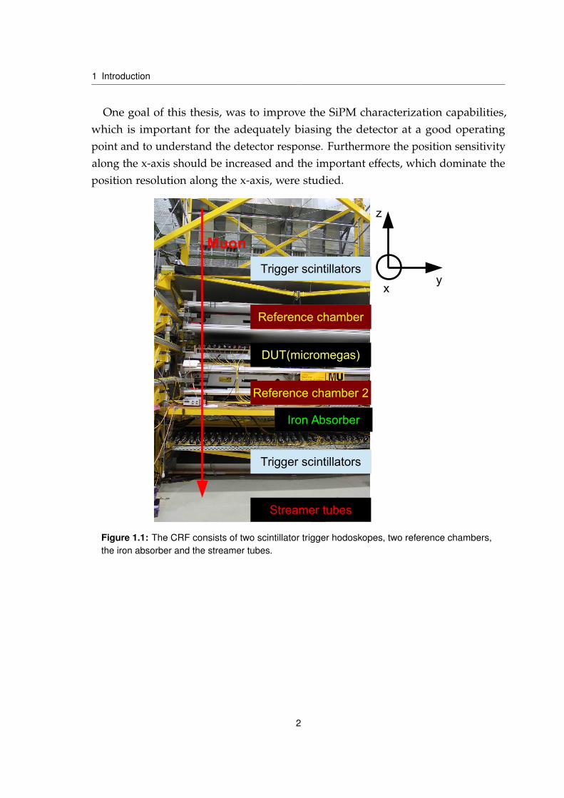
Large area micromegas detectors for the new small wheel upgrade 2018 of theATLAS experiment will be built by the ATLAS collaboration. The LMU Munichparticipates in the construction of micromegas detectors, which will be tested andcalibrated in the CRF (see Biebel et al. [2003]), figure 1.1, in Garching. The CRFtracks high energetic muons with two reference drift chambers with accuracy of50 µm. A veto on the low energetic muons is generated by the streamer tubes,which are used to measure the multiple scattering angle of the muons after passinga 34 cm thick iron absorber. In this way a threshold on the minimum energy of themuons of 600 MeV can be set [Biebel et al., 2003]. The streamer tubes have somedisadvantages and it is planned to replace them by a scintillating detector withSiPM readout (POSSUMUS project, see [Ruschke, 2014]), which will be positionsensitive in two directions. The goal is to achieve a position resolution of 5 mm iny-direction and of 5 cm in the x-direction. The POSSUMUS detector is a prototypedetector, newly developed at the LMU Munich. The idea of the detector is, tocombine two optically insulated trapezoidal scintillator rods. The light produced bythe incoming particles is collected by scintillating fibers and guided to the doublesided SiPM readout. The position resolution along the y-axis is achieved usingthe difference in the light output of the two scintillator rods, which is due to thetrapezoidal shape. The position sensitivity along the x-axis is obtained using thetime of flight information of the signal.
Several prototypes had been built and beamtimes at CERN had shown, that theresolution along the x-axis is in minimum 15 cm and along the y-axis 5 mm (seeRuschke [2014]).
1
1 Introduction
One goal of this thesis, was to improve the SiPM characterization capabilities,which is important for the adequately biasing the detector at a good operatingpoint and to understand the detector response. Furthermore the position sensitivityalong the x-axis should be increased and the important effects, which dominate theposition resolution along the x-axis, were studied.
Trigger scintillators
Trigger scintillators
Reference chamber 1
Reference chamber 2
Reference chamber
Streamer tubes
Iron Absorber
DUT(micromegas)
Muon
yx
z
Figure 1.1: The CRF consists of two scintillator trigger hodoskopes, two reference chambers,the iron absorber and the streamer tubes.
2
CHAPTER 2
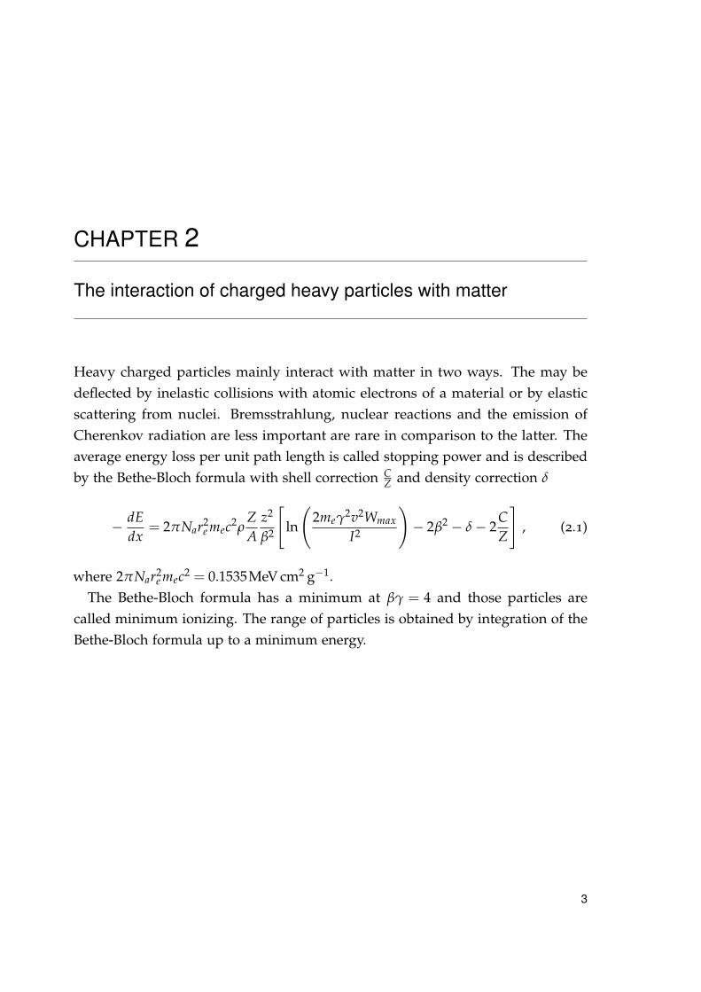
The interaction of charged heavy particles with matter
Heavy charged particles mainly interact with matter in two ways. The may bedeflected by inelastic collisions with atomic electrons of a material or by elasticscattering from nuclei. Bremsstrahlung, nuclear reactions and the emission ofCherenkov radiation are less important are rare in comparison to the latter. Theaverage energy loss per unit path length is called stopping power and is describedby the Bethe-Bloch formula with shell correction C
Z and density correction δ
− dEdx
= 2πNar2e mec2ρ
ZA
z2
β2
[ln
(2meγ
2v2Wmax
I2
)− 2β2 − δ− 2
CZ
], (2.1)
where 2πNar2e mec2 = 0.1535MeV cm2 g−1.
The Bethe-Bloch formula has a minimum at βγ = 4 and those particles arecalled minimum ionizing. The range of particles is obtained by integration of theBethe-Bloch formula up to a minimum energy.
3

2 The interaction of charged heavy particles with matter
Symbol Meaningre classical electron radiusme electron massNa Avogadro numberI mean excitation potentialZ atomic number of absorbing materialA atomic weight of absorbing materialρ density of absorbing materialz charge of incident particle in units of eβ v/c of the incident particleγ 1/
√1− β2
δ density correctionC shell correctionWmax maximum energy transfer in a single collision
Table 2.1: Symbols for the advanced Bethe-Bloch formula (2.1).
4

CHAPTER 3
Basics on SiPM
3.1 Silicon
The material silicon today is one of the most important materials when buildingmodern electronics and one can use it to detect ionizing particles at high precisionas well as for photon-counting at single-photon level.
Material Silicon (Si)Lattice fcc-cubicDensity 2.329 g cm−3
Refractive index 3.42Breakdown field ≈ 3× 10⁵ V cm−1
Band gap 1.12 eVIntrinsic carrier density 9.65× 109 cm−3 [Altermatt et al., 2003]Mean energy for e-h-pair creation 3.63 eVAbsorption coefficient α (see fig. 3.2) 1× 10⁷ m−1 to 1× 10⁵ m−1
Table 3.1: Properties of silicon at 300 K
Silicon is an indirect semiconductor and the electrical properties are related to itsenergy band structure. There are three different principal energy band structuresfor metals, insulators and semiconductors as one can see in figure 3.1. At absolutezero temperature the valence band is completely occupied and the maximumenergy of the highest occupied state is called Ev. Electrons in the valence band arebound and cannot move through the crystal. In analogy there is the conductionband, which is completely empty at zero temperature. The energy of the lowest
5

3 Basics on SiPM
unoccupied state is called Ec. Electrons can move inside the conduction band andbuild up an electrical current. The bandgap is the forbidden area in between. Thereare no allowed energy states available and the with of the bandgap is Eg = Ec − Ev.The difference in electronic behaviour of a material is mainly given by the bandgapenergy Eg. For metals it is Eg < 0, for semiconductors Eg > 0 and for insulatorsEg 0. For silicon, a semiconductor, the valence band is filled and the conductionband is only partly filled, depending on the ambient temperature.
ConductionBand
ValenceBandE
lect
ron
Ene
rgy
Hol
e E
nerg
y
EFermi
B
an
d G
apB
an
d G
ap
EC
EV
Isolator Semiconductor MetalFigure 3.1: Three principal types of band structures - metal, semiconductor and insulator. Onefinds the Fermi energy EFermi, Bandgap energy Eg = Ec − Ev, where Ec is the conduction bandedge energy and Ev is the valence band edge energy
The probability that an orbital at energy E will be occupied in thermal equilibriumis given by the Fermi-Dirac Probability Density Function (PDF) [Kittel and McEuen,1976, p. 136]
f (E) =1
exp[(E− µ)/kBT] + 1(3.1)
with the chemical potential µ, which equals EF (see 3.1) for small temperatures, andthe Boltzmann constant kB = 8.617× 10⁻⁵ eV K−1. The equation (3.1) for electronenergies far greater than the Fermi energy reduces to the Maxwell Boltzmanndistribution:
fe(E) ≈ exp(− E− µ
kBT
), if E− µ kBT (3.2)
6

3.1 Silicon
m]µ [λ0.2 0.4 0.6 0.8 1 1.2
[1/m
]α
1
10
210
310
410
510
610
710
810
910
Figure 3.2: Absorption coefficient of silicon at 300 K taken from Green [2008]. The range ofvisible light in silicon is in the order of a few 0.1 µm for blue light and 10 µm for red light.
For non occupied states in the valence band (holes) the density of states oneobtains in a similar approximation with fe + fh = 1:
fh = 1− fe ≈ exp(− µ− E
kBT
)(3.3)
The use of EF similar to the chemical potential µ is convention in semiconductorphysics. In the conduction band [Kittel and McEuen, 1976, see p. 205]
Ek = Ec + h2k2/2me (3.4)
holds for the electron energy, with Ec the lowest energy inside the conduction band.The density of states in the conduction band for electrons is the number of orbitalsper unit energy range and is given by [Kittel and McEuen, 1976, see p. 205]
De(E) =dNdE
=1
2π2 ·(
2me
h2
)3/2
· (E− Ec)1/2 (3.5)
7

3 Basics on SiPM
where me is the effective electron mass. By convolution of De(E) and fe(E) from(3.2) we obtain the concentration of electrons in the conduction band:
n =
∞∫Ec
De(E) fe(E)dE (3.6)
This integral yields [Kittel and McEuen, 1976, see p. 206]:
n = 2(
mekBT2πh2
)3/2
exp[(µ− Ec)/kBT] = nc exp[(µ− Ec)/kBT] (3.7)
In a similar manner one obtains a formula for the concentration of holes in thevalence band [Kittel and McEuen, 1976, see p. 206]:
p = 2(
mhkBT2πh2
)3/2
exp[(Ev − µ)/kBT] = nv exp[(Ev − µ)/kBT] (3.8)
Multiplication of (3.7) and (3.8) yields
np = 4(
kBT2πh2
)3
(mcmh)3/2 exp(−Eg/kBT) , (3.9)
where µ gets eliminated and the difference Ec − Ev = Eg is equal to the bandgap.The number of electrons equals the number of holes for an intrinsic semiconductorso that one obtains from equation (3.9) [Kittel and McEuen, 1976, see p. 207]
ni = pi = 2(
kBT2πh2
)3/2
(memh)3/4 exp(−Eg/2kBT) (3.10)
as intrinsic density of charge carriers in thermal equilibrium, where the electron-hole pair creation rate equals the recombination rate. For equal effective masses ofelectrons and holes mh = me in the intrinsic case the Fermi level is in the middle ofthe bandgap [Kittel and McEuen, 1976, see p. 207].
µ =12
Eg +34
kBT ln(mh/me) (3.11)
8

3.2 Doped silicon
3.2 Doped silicon
If one deliberately adds impurities to a semiconductor (doping) the material charac-teristics change and the semiconductor shows extrinsic behaviour. In the followingwe consider the case for silicon, which forms four covalent bonds.There are twoways of doping. One adds
• donors, atoms of valence five like P or As, which leave free excess electrons inthe conduction band.
• acceptors, of valence three, like B or Al, which leave positive holes in thevalence band.
Donors (n-type silicon) and acceptors (p-type silicon) introduce states in the forbid-den region (bandgap) and an increase in doping concentration affords an increasein conductivity (see figure 3.3). The Fermi level shifts towards the conductionband for n-type silicon and towards the valence band for p-type silicon. The extraelectrons for n-type material reside in a discrete energy level inside the gap and canbe excited into the conduction band. For p-type material the extra states are createdin the forbidden region near the valence band, which means, that electrons fromthe valence band are excited to this extra level. In this case an electron-hole pairis created and the holes become majority charge carriers for this kind of material.In order to calculate the fermi level, assume that in n-type silicon the electrondensity is given mainly by the donor density Ndonor and, that for p-type materialp ≈ Nacceptor. Using equation (3.7) and (3.8) the shifted Fermi level (EFermi = µ)reads:
EFermi,n = Ec − kBT ln(NC/Ndonor) (3.12)
EFermi,p = Ev + kBT ln(NC/Nacceptor) (3.13)
In the same manner for the charge carrier concentration one obtains:
nn = ni exp(
EFermi,n − EFermi,i
kBT
)(3.14)
np = ni exp(
EFermi,n − EFermi,i
kBT
)(3.15)
9

3 Basics on SiPM
ConductionBand
ValenceBandE
lect
ron
Ene
rgy
Hol
e E
nerg
y
EFermi, n
n-type p-type
EFermi, p
EFermi, i
Figure 3.3: The band structure of p and n-type silicon. In n-type silicon electrons form themajority charge carrier while holes are minority charge carriers, whilst in p-type material this isvice versa.
3.3 The p-n junction
If one joins p-type material and n-type material, the Fermi levels equalize and theenergy bands bend. The boundary of the two regions is called p-n junction (seefig.3.4). The extra electrons from the n-type region drift towards the p-region andfill the holes, while the diffusion is vise-versa for the p-region holes. A net chargebuilds up on either side of the junction and an electric field gradient is created.The net charge is positive for the n-region, negative for the p-region. The fieldgradient leads to a contact potential V0 [Leo, 1994, see pp. 223]. The region nearthe boundary is called depletion zone, which is free of mobile charge carriers.
One can calculate the width of such a depletion zone using the Poisson equationin one dimension,
d2Vdx2 = −ρ(x)
ε, (3.16)
10

3.3 The p-n junction
Ele
ctro
n en
ergy
Cha
rge
dens
ityE
lect
ric fi
eld
Fermi level
n pelectron hole
V0Conduction band
Valence band
Figure 3.4: The p-n junction in a doped semiconductor
11

3 Basics on SiPM
where ε = ε0 × εsilicon.
In the following the author sticks to the derivation of the formulae in Leo [1994,see pp. 224-225]. For simplicity assume a uniform charge distribution along thex-axis for each side,
ρ(x) =
eND 0 < x < xn
−eNA −xp < x < 0 ,(3.17)
where e is the elementary charge and ND and NA are the donor and acceptorconcentrations. For reasons of charge conservation it holds
NAxp = NDxn . (3.18)
By integration of (3.16) and using dV/dx = 0 at x = xn, x = xp one finds
dVdx
= E(x) =
−eNDx + Cn 0 < x < xn
eNAx + Cp −xp < x < 0 .(3.19)
Solving Poisson’s equation piecewise with the correct boundary conditions oneobtains
V0 =e
2ε(NDx2
n + NAx2p) (3.20)
for the contact potential and for the width of the depletion zone [Leo, 1994, see pp.225]
d = xn + xp =
(2εV0
e(NA + ND)
NAND
)1/2
, (3.21)
where Na,Nd is the acceptor and donor concentration, ε is the vacuum permittivityand V0 the contact potential. For the case that NA/ND 1 one can further simplifyequation (3.21) to
d ≈(
2εV0
eND
)1/2
. (3.22)
This holds also, if an external (reverse) voltage is applied, which enlarges thedepletion zone, by replacing V0 with V = V0 + Vext. From (3.22) one obtains
E(x = 0) =
√eNDV
ε=
2Vd
. (3.23)
12
3.4 The Silicon Photomultiplier
3.4 The Silicon Photomultiplier
The first developments for light detection at low intensities with semiconductorswere done by McIntyre [1961] and Haitz [1964], who were studying the effectsof avalanche breakdown and microplasma effects in reverse biased silicon diodes.This research lead to the development of the Avalanche Photo Diode (APD), whichconsists of a reverse biased p-n junction. Incoming particles or photons createelectron-hole pairs, which create further electron-hole pairs and this leads toavalanche generation. The APD has an internal gain in the order of 50 to 500. Forthese devices cooling is mandatory in order to get acceptable signal-to-noise-ratio(SNR) and single photon counting is not possible. The next step was the SiPM (seefigure 3.5,3.6), which is a matrix of APDs biased slightly above Vbd, the breakdownvoltage, in so called Geiger mode and connected in parallel realized first by Golovinand Saveliev [2004] and Buzhan et al. [2003]. A sketch for the charge concentrationof a single microcell can be found in figure 3.7.
3.4.1 Working principle
The initial process for the detection of a photon is the creation of an e-h-pair in theavalanche or drift region of the Geiger mode APD (GM-APD), due to absorption ofa photon. The absorption coefficient of silicon determines the depth of interaction(see figure 3.2). When a single GM-APD is biased slightly above Vbd then theenergy, that the charge carrier gains through the high electric field between twosubsequent collisions, is high enough to generate further electron hole pairs viaimpact ionization (see figure 3.10). Note that the electron component dominatesand ionization by holes is negligible. The microcell APD breaks down dischargingthe accumulated charge completely (see figures 3.8,3.9). The discharge is quenchedby a voltage drop across a quenching resistor Rquench in series with the GM-APD.The equivalent circuit of a cell is given by a capacitance Ccell and a switch inparallel and a quenching resistance Rquench in series. The recharge time constant isτ = Rquench × CCell.
The gain ranges from 1× 10⁵ to 1× 10⁶ and depends on the charge stored onCCell. An estimation for the field strength in the avalanche region can be obtained
13

3 Basics on SiPM
using equation (3.23), which yields 105 V cm−1 for typical width of the depletionzone of 1 µm and bias voltage in the order of 102 V.
3 mm
Figure 3.5: A HamamatsuS10362-33-100C SiPM of size3 mm× 3 mm with 100 µm pixelpitch
substrate
GM-APD
Rquench
Qtot=Q
1+Q
2+...
-Vbias
Vout
Figure 3.6: The equivalent circuitdiagram of a SiPM. A microcell isrepresented by GM-APD with acapacitance Ccell and a resistanceRquench
The advantages of silicon photomultipliers are the high internal gain, smallvolume, the use of standard silicon technology for production, the insensitivityto magnetic fields, good timing properties down to 123 ps [Buzhan et al., 2003,p. 51], photon detection efficiency of about 30 % and SiPM tolerate accidentalillumination. The major drawbacks today are the high dark count rate at singlephoton level, temperature dependence of signal form and gain, complex noisephenomena like optical crosstalk and afterpulses. One chooses the peak sensitivitywavelength of a SiPM by charge concentration profile. For high sensitivity for bluelight, one p-silicon on n-substrate is necessary, for high sensitivity for green lightthe n-silicon on p-substrate configuration is preferred. Doping adjusts the positionof the avalanche region and the position of the drift region of lower electric field,according to the absorption length of the material (see figure 3.2).
14

3.4 The Silicon Photomultiplier
n substrate
microcell structureHamamatsu MPPC
n epitaxial layer
n+p+
p++
0.5 – 1μm
2 – 4 μm
300 μm
E(x)ρ(x)
Figure 3.7: SiPM charge concentrations and field configuration of a single microcell (GM-APD)for a Hamamatsu SiPM. p+ and p++ refer to heavy and extreme heavy doping with more than 1foreign atom per 1000 silicon atoms. [Renker and Lorenz, 2009, see p. 29]
time
space
n-contact
p-contact
electron
hole
time
space
Avalanche Breakdown in Geiger mode
Figure 3.8: When biased above Vbd electron-hole pairs will trigger an avalanche due to impactionization in the high field region of the GM-APD.
3.4.2 SiPM properties
The SiPM is biased above breakdown voltage. The difference Vbias −Vbd = Vover iscalled overvoltage (Vover). A single microcell represents a capacitor (see figure 3.11)and the stored charge divided by e is the single pixel gain
G = Q/e =(Vbias −Vbd)CCell
e. (3.24)
15

3 Basics on SiPM
Cu
rren
t
Reverse voltage
quenching
recharge
avalanche
Vbd V
bias
Proportionalmode
Geiger mode
Figure 3.9: Operating mode a GM-APDaccording to [Dinu, 2013]. Absorption leadsto avalanche discharge, which is quenchedby the voltage drop across Rquench. Thenthe cell is recharged and can be triggeredagain. The read line represents the lineardependence of the signal height on theovervoltage.
Figure 3.10: The impact ionization co-efficients α for electrons and β for holesfrom Musienko et al. [2000]. Avalanchebreakdown is dominated by the electroncomponent.
G is a function of Vover and the temperature. For the differential it holds
dG =∂G∂T
dT +∂G
∂VoverdVover (3.25)
and for dG = 0 one obtains
dVover
dT= −∂G
∂T
( ∂G∂Vover
)−1, (3.26)
which means, that by correct adjustment of Vbias one can compensate temperatureeffects on G.
One refers to a 1 photo electron (PE) signal for a single cell, which is ideallyuniform. All cells are connected in parallel (see figure 3.6) and in this way thereadout signal is the sum signal
S =nc
∑i=1
Si , (3.27)
where nc is the number of microcells on the SiPM.
16

3.4 The Silicon Photomultiplier
The Photon Detection Efficiency (PDE) is the probability than an incoming photonwith certain wavelength is detected. This number was measured to be about 35 %in maximum [Dinu et al., 2009, see p. 424] for the SiPM types used. PDE is theproduct of the ratio of active surface to total detector area, which is the geometricalefficiency εgeom, the trigger efficiency to trigger a microcell εtrigger, when an electronhole pair has been created, and the quantum efficiency QE to create a primaryelectron hole pair.
PDE = QE(λ)× εgeom × εtrigger(λ,Vbias,T) (3.28)
Gain and PDE are related because εtrigger is voltage dependent, which puts a lowerlimit on the feasible Vover. Furthermore the probability for optical crosstalk betweenmicrocells rises for higher Vover. This fakes larger signals and puts an upper limitto Vover. εtrigger is a function of the impact ionization constants for electrons andholes (see figure 3.10). Note that the electron component is dominant, because ofthe lower effective electron mass, which results in greater electron mobility andtherefore electrons gain more energy between subsequent collisions, so that it ismore likely for them to have the required energy for creation of further electron-holepairs and not to loose energy in other collision processes.
The time dependent electric signal of a SiPM consists of a fast and a slowcomponent. The fast component is dominated by the avalanche discharge, whilecell recovery is responsible for the slow one. The cell recovery time τr is determinedby the quenching resistance Rquench and the cell capacitance CCell:
τr ≈ RquenchCcell (3.29)
The sum signal (3.27) has to be corrected for saturation effects. A commoncorrection for the number of triggers ntrigger ignoring the finite recovery time of amicrocell [Pulko, 2012, see p. 12] , as well as crosstalk and afterpulsing, is given by
ntrigger = nc
[1− exp
(PDE× nph
nc
)], (3.30)
where nph is the number of incident photons.
17

3 Basics on SiPM
Figure 3.11: The equivalent circuit for a SiPM at low photon flux taken from Corsi et al. [2006,pg. 1277]. Cd refers to CCell and Rq to Rquench.
Assuming a Gaussian distribution of the microcell capacities one obtains a generalexpression of the charge distribution of short light pulses [Finocchiaro et al., 2009,see p. 5]
f (x) = A×∞
∑i=0
g(i)1√
2πσtot(i)exp
[− (x− c(i))2
2σ2tot(i)
], (3.31)
where
σ2tot = σ2
e + iσ21 (3.32)
c(i) = c0 + ic1 , (3.33)
A is an amplitude, g(i) is the distribution of the number of firing microcells, whichis multiplied by a Gaussian distribution for i-firing cells. σtot(i) accounts for thebroadening of the peaks and c(i) includes the uniform distance of the Gaussianpeaks, which is due to equal charge released by the microcell (see (3.27)). σe isthe electronic noise and σ1 is given by the Excess Noise Factor for a microcellbreakdown, which is a quantity for pixel-to-pixel gain variation. Finocchiaro et al.[2009] propose a Poisson distribution for g(i), in case the SiPM is triggered by
18
3.4 The Silicon Photomultiplier
short light pulses. An elaborate model for g(x) has been developed by Ramilli et al.[2010].
3.4.3 SiPM noise characteristics
The principal issue of understanding the SiPM is to interpret correctly the complexnoise phenomena.
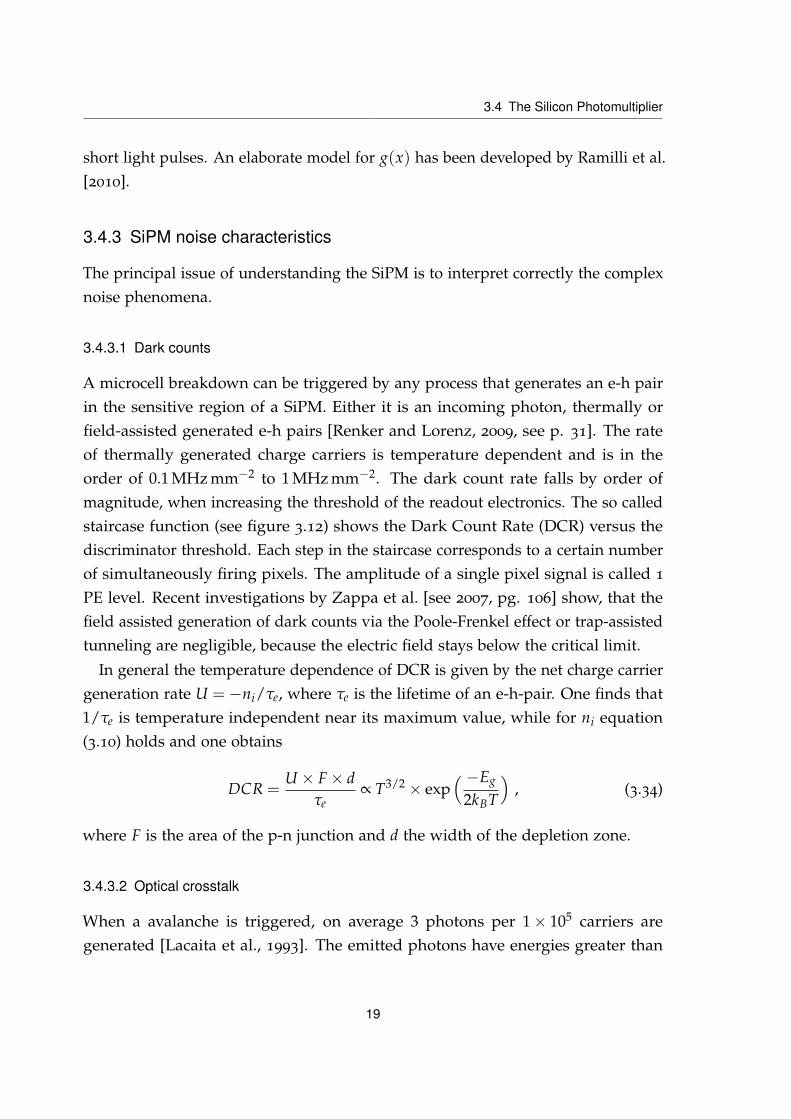
3.4.3.1 Dark counts
A microcell breakdown can be triggered by any process that generates an e-h pairin the sensitive region of a SiPM. Either it is an incoming photon, thermally orfield-assisted generated e-h pairs [Renker and Lorenz, 2009, see p. 31]. The rateof thermally generated charge carriers is temperature dependent and is in theorder of 0.1 MHz mm−2 to 1 MHz mm−2. The dark count rate falls by order ofmagnitude, when increasing the threshold of the readout electronics. The so calledstaircase function (see figure 3.12) shows the Dark Count Rate (DCR) versus thediscriminator threshold. Each step in the staircase corresponds to a certain numberof simultaneously firing pixels. The amplitude of a single pixel signal is called 1
PE level. Recent investigations by Zappa et al. [see 2007, pg. 106] show, that thefield assisted generation of dark counts via the Poole-Frenkel effect or trap-assistedtunneling are negligible, because the electric field stays below the critical limit.
In general the temperature dependence of DCR is given by the net charge carriergeneration rate U = −ni/τe, where τe is the lifetime of an e-h-pair. One finds that1/τe is temperature independent near its maximum value, while for ni equation(3.10) holds and one obtains
DCR =U × F× d
τe∝ T3/2 × exp
( −Eg
2kBT
), (3.34)
where F is the area of the p-n junction and d the width of the depletion zone.
3.4.3.2 Optical crosstalk
When a avalanche is triggered, on average 3 photons per 1× 10⁵ carriers aregenerated [Lacaita et al., 1993]. The emitted photons have energies greater than
19

3 Basics on SiPM
Discriminator Treshold [mV]
Dar
k R
ate
[cps
]
Figure 3.12: The dark count rate as a function of the discriminator threshold for a HamamatsuS10362-11-050C (Ham. 1x1 050C) at different bias voltages from Grossmann [2012]. Eachstep represents a number of simultaneous firing pixels.
the bandgap of silicon and can therefore trigger other cells, which is called OpticalCrosstalk (OC). This process corresponds to the shower fluctuation of an APD[Renker and Lorenz, 2009, see p. 32] and gives a corresponding Excess Noise Factor(ENF) for SiPM. The crosstalk probability is defined as
pcross =DCR1.5pe
DCR0.5pe, (3.35)
where DCR0.5pe is the DCR at 0.5 PE level and DCR1.5pe at 1.5 PE level. Moderndevices use optical trenching to suppress OC. A compromise between acceptablelevel of OC and gain defines the feasible bias voltage.
3.4.3.3 Afterpulsing
When charge carriers are trapped in crystal impurities during an avalanche, oncereleased they can trigger a subsequent avalanche in the microcell up to 100 ns later.In this case an afterpulse (AP) is generated. The lifetime of charge carriers indeep-lying traps is parameterized by two time constants, a short one in the orderof 50 ns and a long one in the order of 150 ns.
20

CHAPTER 4
Scintillation process and plastic scintillators
The plastic scintillator BC-400 used for POSSUMUS prototypes is a transparentmaterial. The working principle for the scintillation process is as follows. Incomingparticles produce a certain amount of photons, which is a function of the energydeposited in the scintillator. For this modern scintillator a nearly linear dependenceof the light output on the energy deposited is found, if quenching effects forheavy particles do not play a role. The amount of light is detected typically by aconventional Photomultiplier or a SiPM, which produces in first order an electricalsignal proportional to the number of impinging photons. The advantages of plasticscintillators are the possibility to obtain almost any desired form, the fast timeresponse and low dead times in the order of a few ns, due to fast recovery times.This is why they are especially suited for triggering purposes.
In general the phenomenon for a material to produce light is called luminescence,which means, that the material absorbs and reemits energy in form of visible light.If the time scale of the reemission is less that 1× 10⁻⁸ s, this is called fluorescence,which is exploited for scintillators [Leo, 1994, p. 158].
Luminescence for organic scintillators is usually based on π-molecular orbitals inbenzene ring structures. The process may start with the absorption of a photon andsubsequent excitation of an electron in the S3 singlet state. Non-radiative internaldegradation leaves the electron in the S1 state, from where the electron has a highprobability of radiative decay to excited vibrational states of S0, which is calledfluorescence (see figure 4.1). These emitted photons cannot be reabsorbed andthis is why the scintillator is transparent to its own radiation (see [Leo, 1994, pp.159-162]). For the triplet states T multipole selection rules forbid the transition to
21

4 Scintillation process and plastic scintillators
Phosphorescence
10 -11 sec
≥10 -4 sec
Fluorescence
~10 -8 10 -9sec
T1
S2
S1
S0
S3
T2
non-radiative
S00
S10
S20
S30
S01
S02
S03
S11
S12
S13
Figure 4.1: The scintillation principle with singlet and triplet states taken from White [1988].
the S0 state and the decay is realized by interaction with another excited molecule(see White [1988],Leo [1994, pg. 162]).
T1 + T1→ S1 + S0 + phonons
In this process one of the molecule ends in the S0 state and the decay is as mentionedbefore, which results in the delayed component of scintillation light.
22

CHAPTER 5
Wave length shifter and light collection
The produced light in the scintillator may be collected by a wave length shiftingfiber. The WLSF consists of scintillator material, which is enriched with wavelengthshifting components with the principal purpose of trapping the light inside the thinfiber, which is then guided by total reflection along the fiber. The second purposeis to match the wavelength of the emitted light to the wavelength of maximumsensitivity of the photon counter.
The underlying principle of wave length shifting is the Franck-Condon effect,which means, that the atoms in excited state are spatially shifted, such, that thede-excitation with the same energy is forbidden, because there is no wave-functionoverlap between excited state and ground state. Typically a fluor atom is excitedto a vibrational mode of a higher electron level. Via internal degradation thevibrational mode decays to its ground state of the excited electron level. Due tothe spatial displacement of the excited atom the probability for the transition to avibrational mode of the electronic ground state is highest. This transition results ina photon with reduced energy.
Often two or more wave length shifting components are added to a scintillator.A sketch for such a de-excitation process one finds in figure 5.1.
The fiber typically consists of a core material and a cladding material. Therefractive index of the cladding is lower than that of the core. The wave lengthshifted photons are emitted isotropic in all directions. Those emitted with angleslower than the angle for total reflection will exit the fiber at the ends, while theothers are lost. The used WLSF (BCF-92) have a refractive index of ncladding = 1.49
23

5 Wave length shifter and light collection
primary excitation
E1x
S2x
S1x
S0x
S3x
γzS0yS0z
S1y
S2yS2z
S1z
X
Y Z
γx γyE1y
Figure 5.1: The de-excitation based on the Franck-Condon principle with two wavelengthshifters involved from White [1988, pg. 821].
and ncore = 1.60, from which one calculates the angle of total reflection θc via Snell’slaw:
θc = arcsin(ncladding
ncore
)= 68.63° (5.1)
The trapping efficiency one calculates from the probability of a photon to be emittedin the solid angle, where total reflection occurs.
Ptrap =1
4π
(2
2π∫0
dφ
π2−θc∫0
dθ sinθ
)= 0.068 (5.2)
The factor 2 accounts for the two possible directions, where the photon is emitted.Note that the absorption and subsequent emission process is essential for trappingphotons in the fiber. Incoming photons leave the fiber, if no absorption takes place,because they never fulfill the conditions for total reflection.
24

CHAPTER 6
The idea of the POSSUMUS-detector
POSSUMUS means POsition Sensitive Scintillating MUon SiPM detector. The basicprinciple of one detector module is to combine two trapezoidal, long scintillators(see 6.1, thesis Ruschke [2014]). Consider a muon hits the detector from aboveand the amount of light produced is nearly proportional to the path length in thescintillator. Then the photon flux through the end of the fibers is proportional tothe path length.
yx m
uon
WLS-Fiber
TrapezoidalSzintillators
#1
#2
Figure 6.1: A sketch of a POSSUMUS detector module with four WLSF. The x-direction isdefined along the long side of the scintillators.
25

6 The idea of the POSSUMUS-detector
Muon
q1
q2
y
Figure 6.2: The basic principle to obtain a position sensitivity along the y-axis. The amount oflight q1 in the upper trapezoid is greater than q2 in the lower trapezoid.
The position y can be expressed as a function of the amount of light produced inscintillator 1 and 2, q1 and q2. Consider Ztotal the total amount of light produced inboth halves, then it holds Ztotal = q1 + q2 and
y ∝ f(
q1q1 + q2
)≈ q1
q1 + q2+ C ,
where C is an arbitrary constant. Note, that this formula is a rough approximationonly, which ignores the Landau like energy loss of the muons. A more detailedcalculation which includes the complete detector geometry one finds in Müller[2013] and Ruschke [2014].
The time of flight photons need until they exit the WLSF can be used to obtainthe x-position of the incoming particle. Consider tl and tr the arrival time of thephotons at the end of the fiber. The time difference is position sensitive and it holds,
x ∝ ce f f (tl − tr) ,
where ce f f is an effective velocity of light yet including reflections by the scintillatorwalls and by the fiber cladding. The upper limit for ce f f is c0/nscintillator.
26

CHAPTER 7
SiPM characterization
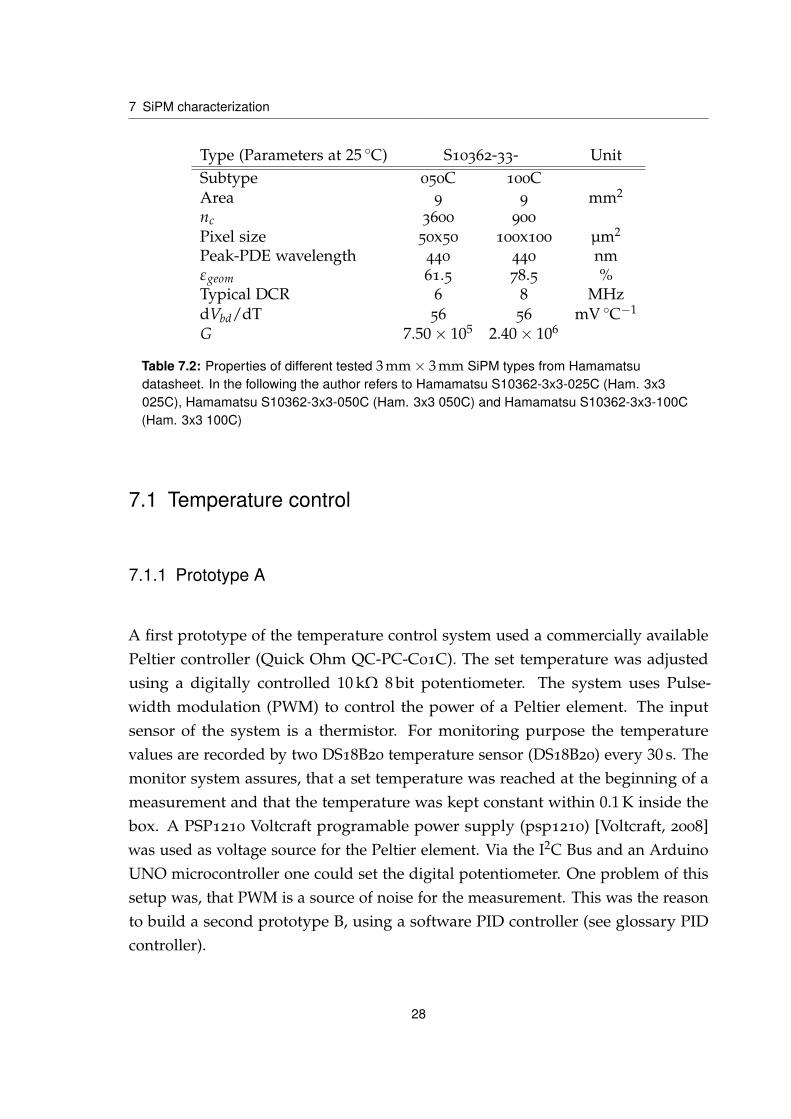
In the first part of this work, methods for the characterization of SiPMs will bepresented. For this purpose a temperature controlled electrically and opticallyinsulated test setup was developed. Temperature controlling is needed, becausethe SiPM quantities like Gain G, quenching resistance Rquench and dark count rateDCR are temperature dependent. Furthermore the vendor of the devices givesrecommendation on Vbias, but there is no information on the breakdownvoltage Vbd,which is essential in order to bias the SiPM at constant moderate Vover to reach aconstant G. The device types in tables 7.1 and 7.2 have been tested.
Type (Parameters at 25 C) S10362-11- UnitSubtype 025C 050C 100CArea 1 1 1 mm2
nc 1600 400 100
Pixel size 25x25 50x50 100x100 µm2
Peak-PDE wavelength 440 440 440 nmεgeom 30.8 61.5 78.5 %Typical DCR 100 150 200 kHzdVbd/dT 56 56 56 mV C−1
G 2.75× 10⁵ 7.50× 10⁵ 2.40× 10⁶
Table 7.1: Properties of different tested 1 mm× 1 mm SiPM types from Hamamatsudatasheet. In the following the author refers to Hamamatsu S10362-11-025C (Ham. 1x1 025C),Ham. 1x1 050C and Hamamatsu S10362-11-100C (Ham. 1x1 100C)
27
7 SiPM characterization
Type (Parameters at 25 C) S10362-33- UnitSubtype 050C 100CArea 9 9 mm2
nc 3600 900
Pixel size 50x50 100x100 µm2
Peak-PDE wavelength 440 440 nmεgeom 61.5 78.5 %Typical DCR 6 8 MHzdVbd/dT 56 56 mV C−1
G 7.50× 10⁵ 2.40× 10⁶
Table 7.2: Properties of different tested 3 mm× 3 mm SiPM types from Hamamatsudatasheet. In the following the author refers to Hamamatsu S10362-3x3-025C (Ham. 3x3025C), Hamamatsu S10362-3x3-050C (Ham. 3x3 050C) and Hamamatsu S10362-3x3-100C(Ham. 3x3 100C)
7.1 Temperature control
7.1.1 Prototype A
A first prototype of the temperature control system used a commercially availablePeltier controller (Quick Ohm QC-PC-C01C). The set temperature was adjustedusing a digitally controlled 10 kΩ 8 bit potentiometer. The system uses Pulse-width modulation (PWM) to control the power of a Peltier element. The inputsensor of the system is a thermistor. For monitoring purpose the temperaturevalues are recorded by two DS18B20 temperature sensor (DS18B20) every 30 s. Themonitor system assures, that a set temperature was reached at the beginning of ameasurement and that the temperature was kept constant within 0.1 K inside thebox. A PSP1210 Voltcraft programable power supply (psp1210) [Voltcraft, 2008]was used as voltage source for the Peltier element. Via the I2C Bus and an ArduinoUNO microcontroller one could set the digital potentiometer. One problem of thissetup was, that PWM is a source of noise for the measurement. This was the reasonto build a second prototype B, using a software PID controller (see glossary PIDcontroller).
28

7.1 Temperature control
7.1.2 Prototype B
The second prototype of the test setup was constructed by carefully insulatingthe Peltier element against the housing. The programmable PSP12010 was usedas current source and the controlling parameters for the software PID controllercould be adjusted manually. The temperature was constant within 0.1 K. A opensource PID controller code was adapted. The achieved temperature range is from5 C to 60 C. For reasons of stability and simplicity the controller was realizedas PI-controller. The controller output was the set current for the Peltier element.The controller gain was set to KP = 6A K−1 and with Ti = 62.8s. The direction ofthe current through the Peltier element is controlled via H Bridge (see figure A.8for the wiring diagram) directly in software, so that the system can be used forcooling and heating. A characterization measurement (see figure 7.1) was done anda temperature difference of 26 K with respect to the room temperature of 28 C wasachieved at a current of 10 A. Figure 7.2 shows the temperature curves for differentcontroller setpoints. It takes about 200 s until the temperature has settled.
U [V]0 1 2 3 4 5 6 7 8 9 10 11 12 13
I [A
]
0
1
2
3
4
5
6
7
8
9
10
C]
°T
[
0
2
4
6
8
10
12
14
16
18
20
22
24
26
28
30
I vs U
T vs U
Figure 7.1: Current voltage characteristicfor the 50 mm× 50 mm Peltier element Hbridge combination. The recorded temper-atures are measured inside the box in ther-mal equilibrium. As long as the nonlineari-ties of the U-I line are small PI-controlling ispossible.
t [s]0 100 200 300 400 500 600 700 800 900 1000 1100 1200
C]
°T
[
0
5
10
15
20
25
30
35
40
45
50
Figure 7.2: T [C] vs time [s] for differentcontroller setpoints. The temperature iskept constant with 0.1 C accuracy. Thecurves refer to the setpoints 6, 10, 14, 16,20, 24, 28, 32, 36 and 40 C. Controllingstarts at 75 s
29
7 SiPM characterization
7.2 Static characteristic
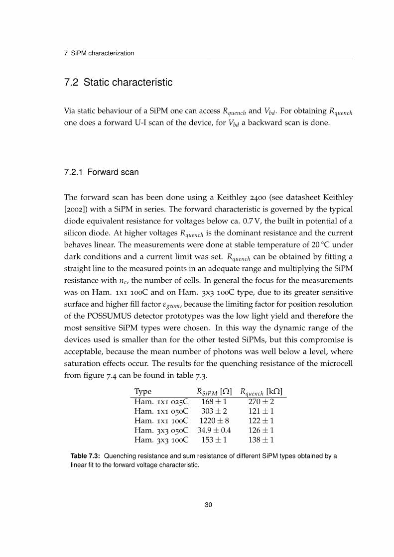
Via static behaviour of a SiPM one can access Rquench and Vbd. For obtaining Rquench
one does a forward U-I scan of the device, for Vbd a backward scan is done.
7.2.1 Forward scan
The forward scan has been done using a Keithley 2400 (see datasheet Keithley[2002]) with a SiPM in series. The forward characteristic is governed by the typicaldiode equivalent resistance for voltages below ca. 0.7 V, the built in potential of asilicon diode. At higher voltages Rquench is the dominant resistance and the currentbehaves linear. The measurements were done at stable temperature of 20 C underdark conditions and a current limit was set. Rquench can be obtained by fitting astraight line to the measured points in an adequate range and multiplying the SiPMresistance with nc, the number of cells. In general the focus for the measurementswas on Ham. 1x1 100C and on Ham. 3x3 100C type, due to its greater sensitivesurface and higher fill factor εgeom, because the limiting factor for position resolutionof the POSSUMUS detector prototypes was the low light yield and therefore themost sensitive SiPM types were chosen. In this way the dynamic range of thedevices used is smaller than for the other tested SiPMs, but this compromise isacceptable, because the mean number of photons was well below a level, wheresaturation effects occur. The results for the quenching resistance of the microcellfrom figure 7.4 can be found in table 7.3.
Type RSiPM [Ω] Rquench [kΩ]Ham. 1x1 025C 168± 1 270± 2Ham. 1x1 050C 303± 2 121± 1Ham. 1x1 100C 1220± 8 122± 1Ham. 3x3 050C 34.9± 0.4 126± 1Ham. 3x3 100C 153± 1 138± 1
Table 7.3: Quenching resistance and sum resistance of different SiPM types obtained by alinear fit to the forward voltage characteristic.
30

7.2 Static characteristic
Keithley 2400 Picoammeter
RS232
Darkbox
Peltier Cooling
Computer
Figure 7.3: The setup for the measure-ment of the reverse U-I characteristic of anot illuminated SiPM. The voltage sourceis a Keithley 2400 and the current is mea-sured by a Keithley 6515 Piccoammeter.
U [V]0 0.5 1 1.5 2 2.5 3
I [A
]
0
0.01
0.02
0.03
0.04
0.05
050C 3x3100C 3x3
100C 1x1050C 1x1025C 1x1
Figure 7.4: Current voltage forward char-acteristic measured for a bare SiPM with aKeithley 2400 voltage source at 20 C
7.2.2 Reverse scan
Vbd is accesible via the reverse current characteristic. For this the SiPM was con-nected to a test board with two 5 kΩ resistors in series (see figure 7.3). The voltagesource was a Keithley 2400 and the current was measured using a Keithley 6514
electrometer (see datasheet Keithley [2003]). An automatic measurement systemwas developed increasing the sourced voltage until a current of 2 µA was reached.
The current is given by the sum of the single APD signal, which can be describedin a first approximation by the Shockley equation [see Dinu, 2013, pg. 12, 20, 172],
I = Is(eVbiase/(nkBT) − 1) (7.1)
where IS is the reverse bias saturation current, n is the ideality factor between 1 to2. This equation ignores surface effects, carrier generation by thermal excitationinside the depletion zone and for high electric fields the tunneling of charges, aswell as avalanche multiplication process above breakdown [see Dinu, 2013].
31

7 SiPM characterization
The current near the breakdown region has two components (see eq. (7.2)) -surface current and bulk current. For surface effects one has to consider, thatthe maximum electric field region is near the surface of the junction, which iscontaminated with ion impurities during the fabrication process. These impuritiesmay establish a conduction channel over the surface, when ions move in thelatter due to high electric field effects. The bulk current is given by the thermallygenerated e-h pairs. Thermal generation takes place, when crystal impurities actas generation/recombination centers for e-h pairs via indirect transitions in theforbidden bandgap region. For a reverse biased depletion region it holds that thenet charge generation rate U is given by U = ni
τ0, where τo is the effective lifetime of
e-h pairs in the depletion region. Both variables depend on temperature and so Uis a function of T. The approximately linear growth of pre-breakdown current isdue to the growth of the depletion width, which results in greater volume wherecharge carriers are generated in the bulk and contributes linear to Ibulk.
For APD one has to consider a multiplication factor for the amount of charge,that flows through the avalanche region,
Ipn = Isur f ace + Ibulk ×M(Vbias) , (7.2)
where M is the multiplication factor, which is related to G for a GM-APD. So forvoltages below Vbd the current is dominated by the surface leakage component,whereas above breakdown the current is dominated by the bulk component. Anapproximation for the current above Vbd is
IV>Vbd ≈ e× G× DCR ∝ e×Vover ×Vover , (7.3)
because the DCR rises approximately linearly with Vover. To extract a value for Vbd
from the U-I characteristic the following fit function was used:
I(Vbias) = p[1] + p[2]×Vbias + p[3]× θ(Vbias −Vbd)× (Vbias −Vbd)2 (7.4)
This holds for Vbias as long as the avalanche quenching time is much smaller thanthe recharging time constant Rquench × CCell. For higher negative bias voltages thecurrent through the junction approaches the asymptotic value I = Vover(Rquench +
RD) ≈ VoverRquench, where RD is the variable diode cell resistance, and the amount
32

7.2 Static characteristic
of charge contained in a single pulse increases more than linearly, because theavalanche quenching time increases with Vover [Dinu, 2013, p. 31]. This nonlinearbehaviour is also amplified by the increase of afterpulsing processes with higherVover.
U [V]60 62 64 66 68 70 72 74
I [A
]
-1010
-910
-810
-710
-610
/ ndf 2χ 79.16 / 42
bdV 0.01486± 71.01
p[1] 2.641e-11± -1.302e-09
p[2] 3.841e-13± 2.407e-11
p[3] 1.008e-07± 1.482e-06
/ ndf 2χ 79.16 / 42
bdV 0.01486± 71.01
p[1] 2.641e-11± -1.302e-09
p[2] 3.841e-13± 2.407e-11
p[3] 1.008e-07± 1.482e-06
measurement no 1
measurement no 2
measurement no 3
measurement no 4
measurement no 5
mean
Figure 7.5: Current voltage reverse charac-teristic for a Ham. 3x3 050C in series withtwo 5 kΩ resistors at 20 C. The measure-ment was repeated 5 times for reasons ofreproducibility and combined. From the fitone obtains Vbd = (71.0± 0.2)V.
U [V]60 62 64 66 68 70 72 74
I [A
]
-1110
-1010
-910
-810
-710
-610
/ ndf 2χ 105.2 / 42
p0 0.00606± 69.29
p1 9.699e-12± -4.345e-10
p2 1.447e-13± 6.981e-12
p3 2.183e-08± 4.101e-07
/ ndf 2χ 105.2 / 42
p0 0.00606± 69.29
p1 9.699e-12± -4.345e-10
p2 1.447e-13± 6.981e-12
p3 2.183e-08± 4.101e-07
/ ndf 2χ 20.58 / 42
p0 0.02969± 70.74
p1 2.857e-12± -1.179e-10
p2 4.156e-14± 2.38e-12
p3 1.472e-10± 1.64e-09
/ ndf 2χ 20.58 / 42
p0 0.02969± 70.74
p1 2.857e-12± -1.179e-10
p2 4.156e-14± 2.38e-12
p3 1.472e-10± 1.64e-09
/ ndf 2χ 625.2 / 66
p0 0.009352± 70.77
p1 1.582e-11± -1.888e-09
p2 2.326e-13± 3.015e-11
p3 2.258e-08± 5.497e-07
/ ndf 2χ 625.2 / 66
p0 0.009352± 70.77
p1 1.582e-11± -1.888e-09
p2 2.326e-13± 3.015e-11
p3 2.258e-08± 5.497e-07
/ ndf 2χ 128.2 / 44
p0 0.01565± 70.96
p1 5.959e-12± -3.343e-09
p2 8.672e-14± 5.464e-11
p3 1.976e-07± 3.003e-06
/ ndf 2χ 128.2 / 44
p0 0.01565± 70.96
p1 5.959e-12± -3.343e-09
p2 8.672e-14± 5.464e-11
p3 1.976e-07± 3.003e-06
100C 1x1
025C 1x1
050C 3x3
100C 3x3
Figure 7.6: The U-I reverse charac-teristic for the tested SiPM types. The3 mm× 3 mm models have greater leak-age currents, because of the difference inarea. The Ham. 3x3 100C type shows thesteepest increase of current above Vbd.
Each U-I measurement is the combination of 5 repetitions (see figure 7.5). Figure7.6 shows U-I characteristics for different SiPM types - green for Ham. 1x1 025C,red for Ham. 1x1 100C, blue for Ham. 3x3 050C, orange for Ham. 3x3 100C. Greaterpixel size lead to steeper increase in current, because the single cell avalanchecontains more charge and the DCR per area is greater for greater pixel sizes. If oneassumes that U and the doping profile is similar for the different types, then therate of charge carriers produced per area is the same and this leads to a greatercurrent for higher pixel sizes. From the fitted function (7.4) one obtains Vbd. Theproblem of this fit, is, that the parameters must be preset carefully to obtain goodfit results and that the range of the fit region is not clearly defined. In this case arange of up to 1 V above a estimated breakdown point and 2 V below this point
33

7 SiPM characterization
was used. A general expression for the nonlinear behaviour above Vbd was notfound in the literature, . The two resistors in series have only small influence onthe measured values, but they prevent accidental overbias. The fit parameter errorfor Vbd underestimates the error. The accuracy for Vbd is about 0.2 V and far greaterthan the errors from the fit, because the fit is sensitive to changes in the preset Vbd
values.
U [V]67 68 69 70 71 72
I [A
]
-1010
-910
-810
-710
-610
/ ndf 2χ 105.2 / 42
p0 0.006981± 70.18
p1 9.022e-13± -3.981e-10
p2 1.329e-14± 7.622e-12
p3 2.039e-08± 4.074e-07
/ ndf 2χ 105.2 / 42
p0 0.006981± 70.18
p1 9.022e-13± -3.981e-10
p2 1.329e-14± 7.622e-12
p3 2.039e-08± 4.074e-07
/ ndf 2χ 88.9 / 42
p0 0.0119± 70.42
p1 7.202e-12± -4.664e-10
p2 1.056e-13± 9.119e-12
p3 3.239e-08± 5.332e-07
/ ndf 2χ 88.9 / 42
p0 0.0119± 70.42
p1 7.202e-12± -4.664e-10
p2 1.056e-13± 9.119e-12
p3 3.239e-08± 5.332e-07
/ ndf 2χ 105.3 / 42
p0 0.01806± 70.58
p1 7.247e-12± -3.424e-10
p2 1.06e-13± 7.564e-12
p3 3.221e-08± 4.323e-07
/ ndf 2χ 105.3 / 42
p0 0.01806± 70.58
p1 7.247e-12± -3.424e-10
p2 1.06e-13± 7.564e-12
p3 3.221e-08± 4.323e-07
/ ndf 2χ 107.7 / 42
p0 0.01167± 70.72
p1 1.75e-11± -1.056e-09
p2 2.555e-13± 1.884e-11
p3 7.21e-08± 1.197e-06
/ ndf 2χ 107.7 / 42
p0 0.01167± 70.72
p1 1.75e-11± -1.056e-09
p2 2.555e-13± 1.884e-11
p3 7.21e-08± 1.197e-06
/ ndf 2χ 63.69 / 42
p0 0.01504± 70.91
p1 3.389e-11± -7.882e-10
p2 4.934e-13± 1.568e-11
p3 6.134e-08± 8.964e-07
/ ndf 2χ 63.69 / 42
p0 0.01504± 70.91
p1 3.389e-11± -7.882e-10
p2 4.934e-13± 1.568e-11
p3 6.134e-08± 8.964e-07
/ ndf 2χ 128.2 / 44
p0 0.01565± 70.96
p1 5.959e-12± -3.343e-09
p2 8.672e-14± 5.464e-11
p3 1.976e-07± 3.003e-06
/ ndf 2χ 128.2 / 44
p0 0.01565± 70.96
p1 5.959e-12± -3.343e-09
p2 8.672e-14± 5.464e-11
p3 1.976e-07± 3.003e-06
/ ndf 2χ 79.16 / 42
p0 0.01486± 71.01
p1 2.641e-11± -1.302e-09
p2 3.841e-13± 2.407e-11
p3 1.008e-07± 1.482e-06
/ ndf 2χ 79.16 / 42
p0 0.01486± 71.01
p1 2.641e-11± -1.302e-09
p2 3.841e-13± 2.407e-11
p3 1.008e-07± 1.482e-06
Hamamatsu 3x3 100C C° 7.9 C°10.7 C°12.6 C°15.5 C°18.3 C°19.9 C°20.0
Figure 7.7: Current voltage reverse characteristic for a Ham. 3x3 100C SiPM in series with two5 kΩ resistors at different temperatures. The temperature dependence of the leakage currentand of Vbd is clearly visible.
34

7.3 Dynamic characteristics
Temperature studies for the Ham. 3x3 100C type have been done in order toinvestigate Vbd(T) and one can recognize the influence of temperature changes inthe U-I characteristic (see fig. 7.7). From this measurement a temperature coefficientdVbd/dT of (66± 1)mV K−1 was obtained (see figure 7.8). An alternative way ofmeasuring dVbd/dT and the interpretation of the results is presented in chapter 7.3.
C]°T [
8 10 12 14 16 18 20
[V
]b
dV
70.1
70.2
70.3
70.4
70.5
70.6
70.7
70.8
70.9
71 / ndf 2χ 37.49 / 4
p0 0.01517± 69.68
p1 0.001079± 0.06614
/ ndf 2χ 37.49 / 4
p0 0.01517± 69.68
p1 0.001079± 0.06614
Figure 7.8: The temperature coefficient of a Ham. 3x3 100C via U-I characteristic, assuming alinear behaviour.
7.3 Dynamic characteristics
For the dynamic characteristics various SiPM were illuminated with short 8 nsLED light pulses [Caen, 2011a], such that the amount of triggered microcells wassmall (1 to 10 PE). The SiPM was mounted to a preamplifier board designed byProthmann [2008, see pg. 22]. The amount of charge generated by a light pulsewas recorded via a CAEN V792 12 bit QDC [Caen, 2010] within a 45 ns integration
35

7 SiPM characterization
gate. Considering the preamplifier Gain of 19.0 dB (amplitude ratio 8.91), the QDCconversion factor for the SiPM charge is:
Q[C](QDC− chan) =4004096
× 18.91× 1pC
QDC− chan(7.5)
= 11.0× 10⁻³ pCQDC− chan
(7.6)
The LED-driver triggers the QDC-readout (see fig. 7.10). Using this method, chargespectra have been recorded at different Vover and temperatures for different SiPMtypes. A picture of the setup in figure 7.9.
The obtained charge spectrum (see 7.11) is described by equation (3.31). In the socalled finger spectrum one can clearly differentiate the number of microcells firingduring a light pulse. Each peak represents a certain number of simultaneouslytriggered microcells. The left peak is called pedestal, when no cells have beentriggered. For this analysis 11 peaks are fitted with a multigaussian fitfunctionplus a gaussian background (7.7) and from the fit a probability distribution for thenumber of firing microcells was obtained, which is used in chapter 9. The gaussianbackground accounts for surface currents and dark counts, which smear out thegaussian peaks.
f (x) = Abg ×N (µbg,σ2bg) +
npeaks f ound
∑i=1
Ai ×N (µi,σ2i ) (7.7)
N is a standard normal distribution. The spectra series contain information onG, dG/dV, dG/dT, the crosstalk probability pcross, and via the distribution of thenumber of firing microcells one obtains the distribution for the mean number ofimpinging photons (see pg. 15).
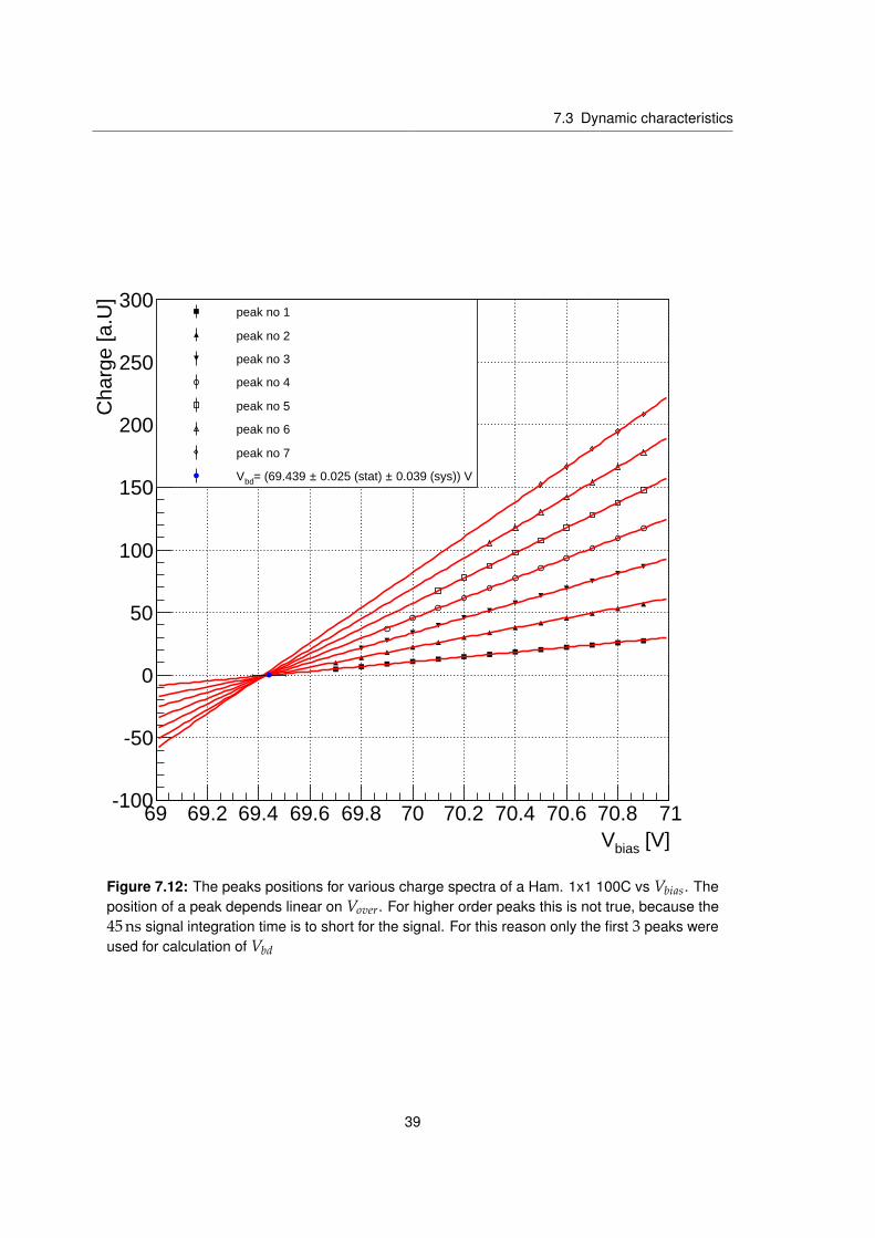
Figure 7.12 shows the peak positions at different Vover relative to the pedestalpeak. The fitted linear functions intersect at the breakdown point. The slope ofthe linear function of peak number 1 is proportional to dG/dV. In this work thebreakdown voltage is calculated as the mean of the intersections of the lines from 1to 3 PE. The reason why not more lines were used, is the fact, that the peak positionsfor higher order peaks do not depend linear on Vover, because the integration timeis too short. But significantly longer integration times are not feasible, because dark
36

7.3 Dynamic characteristics
SiPM
WaveguideT-Sensor
Figure 7.9: The setup for the SiPM charac-terization at low photon flux. The ClearWave Guide (CWG) guides the lightpulses with peak intensity at 400 nm. TwoDS18B20 sensors were used to monitorthe temperature inside the box.
VME
Fan In Fan Out
DarkboxSiPM-Board
Peltier Cooling
Fan In Fan Out
Cooler
Fan In Fan OutLED Driver
Fan In Fan OutDual Delay
Fan In Fan OutQDC
Low Threshold Discriminator
Clear Wave Guide
Dual Timer
Sig
nal
reset
I/O RegisterPCI to VME
NIMGate/Trigger
TTL
inv. TTL
Computer
Figure 7.10: The readout scheme for theQDC-spectra.
counts prevent resolving the peaks and a spurious background builds up in thecharge spectrum (see 7.11). The values for the tested SiPMs can be found in tableA.1. The statistical error for the determined breakdown voltage is as follows,
(∆Vbd)2 =
19
3
∑i=1
[(∆bi
ai
)2+(bi∆ai
a2i
)2]
(7.8)
where ai and bi correspond to slope and intercept of the ith line. Combining thiswith the systematic error of the voltage source (see Keithley [2002]) one obtains:
Vbd = (69.439± 0.025(stat)± 0.039(sys))V (7.9)
For the Ham. 3x3 100C dG/dV(T = 20K) ≈ 8× 10⁵ V−1. Consider a typicalVover = 1.5V, a compromise between PDE and crosstalk then it holds in the linearapproximation:
dG/dVG
= 1/Vover ≈ 0.067% mV−1
37

7 SiPM characterization
Charge [a.U]0 50 100 150 200 250 300 350
Co
un
ts
0
2
4
6
8
103
10×
Figure 7.11: QDC spectrum (black) of a Ham. 1x1 100C at Vover = 0.6V with the multigaus-sian fitfunction (red) with gaussian background (green). The conversion factor for charge is400/4096 pC per bin with preamplifier gain of 8.91.
This implies that the voltage source should be stable at the level off ca. 10 mV, thateffects due to gain variations stay low. Higher Vover lead to significant increase incrosstalk and DCR and a compromise must be made.
Temperature studies show a temperature coefficient for the Ham. 1x1 100C of(60.8± 0.6)mV K−1 (see figure 7.13), which is in good accordance to the valuemeasured with via the U-I method (see section 7.2.2). Deviations are probablydue to the problematic fit procedure used for the U-I-characteristic. The signalheight variation due to the temperature dependence of the BGA614 Darlingtonpreamplifier gain is negligible. The bias resistance used for the amplifier was68 Ω at Vcc = 5V [see Prothmann, 2008]. The temperature testing range was fromapproximately 0 C to 30 C, which implies a variation in device current of about
38
7.3 Dynamic characteristics
[V]biasV69 69.2 69.4 69.6 69.8 70 70.2 70.4 70.6 70.8 71
Cha
rge
[a.U
]
-100
-50
0
50
100
150
200
250
300peak no 1
peak no 2
peak no 3
peak no 4
peak no 5
peak no 6
peak no 7
0.039 (sys)) V± 0.025 (stat) ±= (69.439 bdV
Figure 7.12: The peaks positions for various charge spectra of a Ham. 1x1 100C vs Vbias. Theposition of a peak depends linear on Vover. For higher order peaks this is not true, because the45 ns signal integration time is to short for the signal. For this reason only the first 3 peaks wereused for calculation of Vbd
39

7 SiPM characterization
1 mA. The resulting variation in power gain is less than 0.1 dB at 19 dB [seeProthmann, 2008, pg. 35], which results in a temperature coefficient for the powergain variation in the order of 0.1 % K−1. One concludes that the dominant factorfor variations in the SiPM signal is the SiPM temperature coefficient.
C]°T [5 10 15 20 25
Ub
d [
V]
68.6
68.8
69
69.2
69.4
69.6
69.8 / ndf = 2.381 / 32χ
p0 0.008526± 68.33 p1 0.0005862± 0.06083
Figure 7.13: The temperature coefficient dVbd/dT determined via charge spectra series at 5different temperatures.
The reason why this temperature coefficient is positive, is the temperature de-pendence of ionization probability per unit distance travelled α (impact ionizationcoefficient), which is a function of εr, the optical phonon energy, εi, the ionizationenergy, and λ the mean free path for generation of optical phonons. Using Barraffstheory Crowell [1966] showed, that in the high field region the temperature depen-dence of the ionization rate is dominated by a variation in λ, while the energy lostper unit path is nearly independent of the temperature. For higher temperaturesthe mean free path is smaller, which means, that a smaller fraction of the carriers
40

7.3 Dynamic characteristics
reach the energy necessary to generate further ionization, which results in a positivetemperature coefficient for Vbd.
41


CHAPTER 8
SiPM gain stabilization
For SiPM it is essential to monitor and control Vover, because G and PDE dependon this parameter unlike for photomultipliers, where gain and quantum efficiencycan be adjusted separately. The temperature dependence of G was investigated inchapter 7. The results show the greatest values for dG/dV for the 100 µm Pixelsize type. For the POSSUMUS detector, no active temperature control of the setupwas applied and in this way a controlling mechanism for Vbias was required. Testmeasurements with the setup and readout from figures 7.9,7.10 were done, inorder to check the performance of linear gain stabilization (see figures 8.2,8.2) andshowed that the temperature dependence was reduced. Then a multichannel gainstabilization system was built, using 8 bit 20 kΩ RDAC as voltage divider for 5 V.The input of the temperature sensor, which is mounted on the metal beam next tothe SiPM, is used with the temperature coefficient dVbd/dT = 60mV K−1 to adjustVbias. A sketch of the multichannel gain stabilization system can be found in figure8.1. The system measures and records the temperature for each SiPM and thecontrolling threshold is a minimum temperature change of 0.3 K, limited by theresolution of the RDAC. Calibration measurements have been performed with theprogrammable voltage divider to check the uniformity of channels (see A.3). A longterm measurement of 7 days was done to test the performance of the multichannelgain stabilization system. G is stabilized at best within σ at 0.92 % of the set Gvalue (see table 8.1).
The design value of 20 kΩ for the maximum was chosen such, that under aload similar to a Ham. 3x3 100C the output voltage shows linear behaviour. Theminimum load resistance is in the order of Rload ≈ 70V/100µA = 700kΩ, when the
43

8 SiPM gain stabilization
USB/Serial
Computer
Arduino UNO
I2C MultiplexerPCA9544APW
I2C Digital PotiAD5263
I2C IsolatorADUM 1250
I2C
1
Source 1ca. 5 V
Source 2Ca. 70 V
SIPM
Bia
s 1
I2C
2
I2C
3
I2C
4
4 SiPMs per Poti4 Potis per I2C Bus4 I2C Lines per Multiplexer
Figure 8.1: The multichannel gain stabilization system uses the I2C Bus to steer the voltagedivider. The voltage divider uses a 5 V floating voltage source.
44

SiPM is saturated. The output voltage of the voltage divider with resistance R1, R2
without load is given by Vt =R2
R1+R2V. If one includes the load resistance it reads
Vt =RP
R1 + RPV , (8.1)
where RP = (RloadR2)/(Rload + R2). The deviation of set voltage value from thereal voltage is 25 mV at maximum (see figure A.4) and negligible, for SiPM at lowphoton flux.
C]°T [5 10 15 20 25 30
Cha
rge
[a.U
.]
0
50
100
150
200
250
300 peak no 1peak no 2peak no 3peak no 4peak no 5peak no 6peak no 7peak no 8peak no 9
Figure 8.2: The peaks of the charge dis-tribution spectra at different temperaturesand constant Vbias
C]°T [5 10 15 20 25 30
Cha
rge
[a.U
.]
0
50
100
150
200
250
300 compensation03.datpeak no 1peak no 2peak no 3peak no 4peak no 5peak no 6peak no 7peak no 8peak no 9
Figure 8.3: The peaks of the charge dis-tribution spectra with temperature com-pensation via adjustment of Vbias using60 mV K−1. For this measurement thesetup from chapter 7.3 was used.
Channel no. RMS/Mean UnitUncompensated Compensated
0 4.5 0.92 %1 4.7 1.3 %2 5.7 0.97 %3 6.3 1.3 %
Table 8.1: The goodness of G controlling algorithm. The values calculated with the measure-ment from figures A.6, A.7
45

8 SiPM gain stabilization
t [dd/hh]03/02 04/02 05/02 06/02 07/02 08/02 09/02
G [
a.U
]
10
11
12
13
14
15
16
17 C]
°T
[
18
20
22
24
26
28
Figure 8.4: Gain monitoring without Vbiascorrection. The measurements were per-formed using a programmable LTD, switch-ing between low threshold for Gain de-termination and the threshold for cosmicrays. For details see thesis Ruschke [2014].Temperature recording started only later inthe measurement.
t [dd/hh]01/01 02/01 03/01 04/01 05/01 06/01
G [
a.U
]
10
11
12
13
14
15
16
17 C]
°T
[
18
20
22
24
26
28
Figure 8.5: The peaks of the charge distri-bution spectra, when compensating tem-perature changes via adjustment of Vbiasusing 60 mV K−1. The multichannel gainstabilization system uses the I2C Bus steerthe 5 V floating voltage divider.
In figure 8.4 one can clearly recognize the day-night temperature variations inthe lab. When the temperatures drop, G increases, whereas in figure 8.5 there is nolong term trend visible and G fluctuates around a constant value.
46

CHAPTER 9
Model for the SiPM response
For the SiPM detector response function one has to consider, the distribution ofthe number of incoming photons, dark count rate (DCR), optical crosstalk (OC),photon detection efficiency (PDE). According to Ramilli et al. [2010] a simplemodel assumes a Bernoullian detection process, with the parameter PDE for asingle photon to trigger an avalanche during the integration time. In this casethe probability distribution of triggered microcells is given by a sum over theproduct of the distribution of impinging photons with a Binomial distribution. OCcan be described as cascade phenomenon by a constant probability at a certainVover for one cell to trigger another one, independent of the number of previouslytriggered cells and geometry effects. The time dependence of this process is alsocompletely omitted, which is a good assumption, as long as the signal integrationtime is long in comparison to the time scale of OC. Several authors [Eckert et al.,2010, Finocchiaro et al., 2009, Ramilli, 2008] propose Poissonian statistics for thephoton number distribution of a pulsed LED at low light intensities, which isdirectly connected to the initial distribution for the number of firing cells via PDE.This hypothesis is based on the assumption that the registration of photons isstatistically independent during the counting interval [see Teich and Saleh, 1991, pg.403,404]. Deviations from this behaviour originate in correlated events. These threeparameters - λPoisson,PDE, pcross - were used to generate a Monte-Carlo sampleaccording to figure 9.1 in order to test the Poissonian hypothesis. Minimizingchisquare (see chapter A.1) the best fit-distribution was found, extracting thenormalized probability distribution of equation (7.7) for the number of firingmicrocells from the finger spectrum in figure 7.11. Dark counts during the counting
47

9 Model for the SiPM response
interval of 45 ns are unlikely to happen at DCR in the order of 1 MHz and contributeabout a few % to the mean value of the distribution of firing cells. For the spectrumof this SiPM data were available also on the value for pcross(Vover = 1.1V) = 0.3,taken from Bollu [2014, see pg. 29,30], which was used to fix pcross, for theminimization procedure. This was necessary, because a the global minimumfor chisquare does not show sensible results for the model parameters.
Poisson distributed (mean λ)
number of photons i
p=PDEMicrocell triggered?
YE
S
j=j+1
p=pcross
Crosstalk + Afterpulse?
k=0;k<i
NO
Number of triggered Microcells j=j+1
YE
S
NO
k++
Figure 9.1: A simple model for the detector response using the Poisson hypothesis for low lightintensities from pulsed LEDs.
The comparison of data and Monte-Carlo sample (see figure 9.2,9.3) reveals, thatthere is a good agreement for a higher number of firing cells, while especially at0 to 3 firing cells, the agreement is not perfect. This may be an effect of omittingthe spurious dark counts, which are indistinguishable from real hits. Dark countsresult in a smaller probability for 0 firing cells and in greater probabilities for 1 andmore firing cells. The fundamental difference to OC is, that for OC the 0 bin is not
48

affected, but true photon hits and OC events are shifted to higher bin numbers.For OC no upper limit of the maximum triggered cells was used, because thenumber of triggered cells is small compared to the total number of cells and evenfor higher order OC the density of triggered cells around the initially triggered cellstays small [see Otte, 2007, pg. 158]. More elaborated models for OC have beendeveloped by Otte [2007], but these require a detailed knowledge about the dopingconcentrations in the cell structure, which is not provided by the vendor, as well asknowledge on the emission process of photons produced in the avalanche discharge.The latter includes the energy spectrum and the intensity of the emitted photonsduring the avalanche, which are object of actual research. The parameters obtainedby the minimization procedure are PDE = 0.37 at Vover = 0.6V and λPoisson = 4.2.Comparing with the value of PDE = 0.42 measured at Vover = 1.4V by Dinu [see2013, pg. 65], the minimization leads to sensible values. In this way an alternativemethod was found to obtain λPoisson, which is quite commonly determined usingthe information in the 0 bin with the total number of entries only and determiningthe number of incoming photons as λPoisson = − ln
NpedNtot
, where Nped corresponds tothe number of entries in bin 0 and Ntot represents the total number of entries in thehistogram [Enzweiler, 2013, Glauß, 2012].
The chisquare plots (figure 9.4,9.5,9.6, note the logarithmic color axis.) withone parameter fixed show, that λPoisson and pcross are anti-correlated, which is theexpected behaviour, because crosstalk fakes photon signals and this leads to anoverestimation of λPoisson (see figure 9.4). From figure 9.5 one concludes, the higherthe mean of the incoming photons is reconstructed the less PDE is assumed. Thisresult is at first sight astonishing, but may be connected to the Poisson hypothesisand the shape of the initial photon number distribution. It is probable that darkcounts may cause this kind of behaviour, because of effects on the shape of thephoton distribution, especially in the first bins. Figure 9.6 indicates that higherpcross is connected to lower PDE, because given a higher crosstalk, which triggersadditional cells, one may estimate lower values for PDE.
The Monte Carlo model showed, that it is problematic to determine the meannumber of impinging photons with the number of entries in the 0 bin. A possibleextension of the model is to use also the data on dark count rate, which may haveeffects on the discrepancies in the first bins.
49

9 Model for the SiPM response
#firing microcells0 2 4 6 8 10
freq
uen
cy
0
0.02
0.04
0.06
0.08
0.1
0.12
0.14
0.16
0.18
0.2
=4.2poissλ=0.3, cross
pde=0.37, p
MC-simulation
Data
Figure 9.2: Data vs MC-simulation fora Poissonian number of photons in theLED-light pulse and the detector responsemodel as in 9.1.
#firing microcells0 2 4 6 8 10
no
rmal
ized
res
idu
al
-5
-4
-3
-2
-1
0
1
2
3
Figure 9.3: Normalized residuals
poissλ3 3.5 4 4.5 5 5.5 6
cro
ssp
0.1
0.2
0.3
0.4
0.5
0.6
210
310
410
Figure 9.4: Chisquare distribution for pcrossvs λPoisson
Poissλ3 3.5 4 4.5 5 5.5 6
pd
e
0.1
0.15
0.2
0.25
0.3
0.35
0.4
0.45
0.5
210
310
410
Figure 9.5: Chisquare distribution for PDEvs λPoisson
50

crossp
0.1 0.2 0.3 0.4 0.5 0.6
pd
e
0.1
0.15
0.2
0.25
0.3
0.35
0.4
0.45
0.5
210
310
410
Figure 9.6: Chisquare distribution for PDEvs pcross
51


CHAPTER 10
Tests on the time resolution and readout system
One goal for the POSSUMUS detector is a position sensitivity along the long sideof the scintillator rods of 5 cm. In order to check the performance of the readoutsystem, the scintillator rods and the SiPM timing, two scintillating fiber prototypeswere constructed. For the latter BCF-12 scintillating fiber with 3.2 ns decay time,435 nm peak emission and absorption length of 2.7 m with 5 mm diameter (seeSaint-Gobain_Crystals [2014a]) was used. The core refractive index is 1.6, whilethe cladding refractive index is 1.49. This prototypes were tested with a 20 MeVproton beam of 5 mm diameter at MLL-Garching tandem accelerator (see figure10.1) in March 2014 and August 2014. The projected range of the protons along thebeam axis inside a 1.05 g cm−3 polystyrene target (see BCF-12) as given in the NISTPSTAR ([NIST, 2014]) database is 0.41 cm, which means the protons stop inside theprototype.
53

10 Tests on the time resolution and readout system
Figure 10.1: The 20 MeV proton beam hitting a scintillator tile. The 5 mm beamspot is clearlyvisible.
10.1 Photomultiplier-Fiber prototype
For this prototype a 1 m fiber was used and two Hamamatsu R1665 Photomultiplierswere glued to the ends of the optically insulated fiber. The prototype was mountedto a step motor with 5 µm minimum step size. In the experiment 35 cm horizontalmovement was covered in 5 cm steps. The height of the prototype was adjusted tothe position of maximum trigger rate of 170 Hz. The photomulitplier voltages wereset to 800 V and 752 V, such that the pulse heights were equal at the center of thefiber. As voltage source a ISEG SHQ 224M was used (see datasheet ISEG [2014]).
1 mPMT 1 PMT 2Scintillating Fiber
5mm Proton Beam
TDC-Readout
Figure 10.2: A sketch of the setup for test-ing the time-to-digital converter (TDC)readout.
Figure 10.3: The scintillating fiber mountedto the stepper motor at the tandem acceler-ator facility.
54

10.1 Photomultiplier-Fiber prototype
A Caen N845 low threshold discriminator in combination with a Caen N455
coincidence logic unit with coincidence time of 40 ns was used to trigger a CaenV775N 12 bit TDC (see datasheets [Caen, 2004, 2011b, 2012]). One finds a sketch ofthe readout scheme in figure 10.4. The TDC was operated in common stop modeand the full range was set to 143 ns, so that the conversion factor is 34.9 ps perbin. The discriminator threshold was set to 30 mV, well above dark current of thephotomultipliers. One finds the obtained TDC spectra for the different positions infigure 10.5. The right peak is the peak of the 32 ns delayed channel with a width of1 bin standard deviation, which means, that the delay is sufficient and no triggersare generated by the second channel.
VME
TDC
PCI to VME
Common Stop
Computer
DiscriminatorSignal A NIM A
NIM BDelay Coincidence
&
NIM
A
NIM
B
Signal B
Figure 10.4: The TDC readout scheme. For the SiPM experiment a constant fraction discrim-inator with amplitude and risetime compensation triggering and for classical photomultiplier alow threshold discriminator were used.
The arrival time difference of the signals is given by
∆t =ncore
c∆xe f f , (10.1)
where ncore is the refractive index of the core material, c the velocity of light, xe f f
the effective way of light in the fiber accounting for reflections. A Gaussian functionwas fit to each of the spectra from fig. 10.5. The skewness of the distributions atthe edges of the covered range may be an effect of light attenuation in the fiberand the constant threshold trigger technique. Considering the absorption length
55

10 Tests on the time resolution and readout system
Time [a.U]2650 2700 2750 2800 2850 2900
Co
un
ts
0
100
200
300
400
500
600
700
Figure 10.5: The time distribution of the photomultiplier signals at different detector positions.The right peak corresponds to the delayed channel. The step size is 5 cm. One position ismissing. 10000 events were recorded at each position.
of 2.7 m one finds a difference of 12 % in intensity from edge to edge. From figure10.6 one obtains (7.1± 0.4) cm ns−1 for the effective velocity of light. For this value8.5 cm ns−1 has been reported by Chichester et al. [2012] for this material. Thedifference may be a calibration effect of the TDC or, becauseChichester et al. [2012]used a longer piece of fiber. The used TDC was calibrated with a signal and delayedsignal from 2 ns to 40 ns.
56

10.2 SiPM-Fiber prototype
Position [cm]-20 -15 -10 -5 0 5 10 15
t [s
]∆
0
1
2
3
4
5
6
-910×
/ ndf 2χ 0.06599 / 5
p0 9.159e-11± 2.784e-09
p1 7.742e-12± -1.398e-10
/ ndf 2χ 0.06599 / 5
p0 9.159e-11± 2.784e-09
p1 7.742e-12± -1.398e-10
Figure 10.6: The time difference of the arrival times obtained by the Gaussian fit versusthe detector position for the photomultiplier prototype. The effective velocity of light was(7.1± 0.4) cm ns−1.
10.2 SiPM-Fiber prototype
The SiPM-Fiber prototype was built (see figure 10.7) in order to check the SiPMtiming performance in comparison to classical photomultipliers. Two Ham. 3x3
100C SiPM were glued with instant adhesive to a centering plastic structure at thepolished ends of a 35 cm long scintillating fiber. The optically active surface of theSiPM was covered with Roth M500000 silicone fluid (now Wacker, see [Wacker,2013]) with refractive index of 1.40 in order to improve the coupling to the fiber. AsSiPM voltage source two EA PSI 8160-04T (see [Automatik, 2014]) were used. Thereadout electronics was as in figure 10.4, except that in place of the low thresholddiscriminator a programmable Caen V812 constant fraction discriminator (CFD)was used. The CFD uses amplitude and risetime compensating triggering technique(see glossary amplitude and risetime compensation triggering) with 4 ns delay time,accounting for the SiPM signal rise time and 150 ns dead time, which suppressesfurther triggers due to afterpulsing or time walk due to the temperature coefficient
57
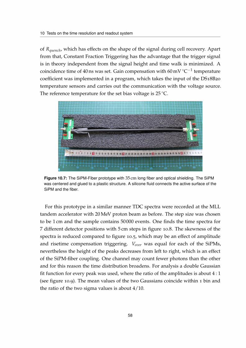
10 Tests on the time resolution and readout system
of Rquench, which has effects on the shape of the signal during cell recovery. Apartfrom that, Constant Fraction Triggering has the advantage that the trigger signalis in theory independent from the signal height and time walk is minimized. Acoincidence time of 40 ns was set. Gain compensation with 60 mV C−1 temperaturecoefficient was implemented in a program, which takes the input of the DS18B20
temperature sensors and carries out the communication with the voltage source.The reference temperature for the set bias voltage is 25 C.
Figure 10.7: The SiPM-Fiber prototype with 35 cm long fiber and optical shielding. The SiPMwas centered and glued to a plastic structure. A silicone fluid connects the active surface of theSiPM and the fiber.
For this prototype in a similar manner TDC spectra were recorded at the MLLtandem accelerator with 20 MeV proton beam as before. The step size was chosento be 1 cm and the sample contains 50000 events. One finds the time spectra for7 different detector positions with 5 cm steps in figure 10.8. The skewness of thespectra is reduced compared to figure 10.5, which may be an effect of amplitudeand risetime compensation triggering. Vover was equal for each of the SiPMs,nevertheless the height of the peaks decreases from left to right, which is an effectof the SiPM-fiber coupling. One channel may count fewer photons than the otherand for this reason the time distribution broadens. For analysis a double Gaussianfit function for every peak was used, where the ratio of the amplitudes is about 4 : 1(see figure 10.9). The mean values of the two Gaussians coincide within 1 bin andthe ratio of the two sigma values is about 4/10.
58

10.2 SiPM-Fiber prototype
Time [a.U]1350 1400 1450 1500 1550 1600
Cou
nts
0
500
1000
1500
2000
2500
3000
3500
4000
Figure 10.8: The time distribution of the SiPM signals at different detector positions. The scanstep size was 1 cm, but for reasons of readability the position difference for the spectra is 5 cm.For each position 50000 events were recorded.
The analysis (see figure 10.10) shows, that the position of the mean values islinearly dependent on the detector position. A slight peak broadening is visible,if the proton beam hits the detector at higher distances to on of the SiPMs. Theovervoltage were set to be equal, so this may only be an effect of different SiPM-fibercoupling.
Table 10.2 shows the mean standard deviation of the Gaussian peaks convertedto a distance with the conversion factor obtained as a combination of the twofiber measurements of 7.15 cm ns−1 (see figure 10.10, 10.6). The obtained positionresolution as well as the measured effective velocity of light of the fiber detectorprototypes are comparable. The effective velocity of light is governed by reflections
59

10 Tests on the time resolution and readout system
Entries 49592
Mean 1477
/ ndf 2χ 163.6 / 94
constant_0 24.0± 2452
mean_0 0.0± 1477
sigma_0 0.06± 5.53
constant_1 21.0± 425.5
mean_1 0.1± 1476
sigma_1 0.19± 13.28
Time [a.U]1300 1350 1400 1450 1500 1550 1600 1650 1700
Cou
nts
0
500
1000
1500
2000
2500
3000 Entries 49592
Mean 1477
/ ndf 2χ 163.6 / 94
constant_0 24.0± 2452
mean_0 0.0± 1477
sigma_0 0.06± 5.53
constant_1 21.0± 425.5
mean_1 0.1± 1476
sigma_1 0.19± 13.28
0
2000
4000
6000
8000
10000
12000
14000
16000
18000
20000
22000
Figure 10.9: The time distribution at position 20.4 cm from the left SiPM, which correspondsto the blue peak in figure 10.8. A double Gaussian fitfunction was used. The green spectrumrepresents pedestal peak.
Distance SiPMA [cm]5 10 15 20 25 30 35
t [s
]∆
-4
-3
-2
-1
0
1-910×
/ ndf 2χ 4.075 / 31
p0 8.694e-11± 7.22e-10
p1 3.537e-12± -1.373e-10
/ ndf 2χ 4.075 / 31
p0 8.694e-11± 7.22e-10
p1 3.537e-12± -1.373e-10
Figure 10.10: The position of the mean values of the dominant Gaussians, with sigma errors.The obtained effective velocity of light is (7.3± 0.2) cm ns−1.
60

10.3 SiPM scintillator block prototype
at the cladding material, and the broadening of the peaks is dominated by thescattering and reflection processes inside the fiber and the time pick-off method ofthe amplitude and risetime compensation triggering.
Prototype σ [cm]Photomultiplier prototype 1.8SiPM prototype Gaussian1 1.2SiPM prototype Gaussian2 2.86
Table 10.1: Mean position resolution at 1σ of the Gaussian fit to the time distribution. Gaus-sian1 and Gaussian2 refer to the double Gaussian used to fit the SiPM fiber prototype data.The values were calculated using the effective velocity of light obtained from the linear fit.
10.3 SiPM scintillator block prototype
Experiments at CERN (see [Ruschke, 2014]) revealed, that the position resolutionfor POSSUMUS via time difference of the signals was about 15 cm. The goal of thisexperiment was to decide, whether direct coupling of the SiPMs to a scintillator isbetter for the position resolution along the x-axis, than the readout via the WLSF.The advantage of direct coupling, is that more direct light hits the SiPM, while forindirect readout, the position, where the photons hit the fiber is uncertain and theabsorption and reemission process broadens the time spectrum. In order to testthis, a POSSUMUS prototype was built. The prototype is based on a 0.6 m long40 mm× 90 mm rectangular BC-400 scintillator rod with a 1 mm diameter BCF-92
WLSF (see datasheet [Saint-Gobain_Crystals, 2014b]) centered at 4.5 cm. The WLSFwas placed in a 1 mm groove and glued to the scintillator rod with optical cementof the same refraction index. As wrapping material aluminum foil was used. Ateach end of the fiber a Ham. 3x3 100C SiPM (SiPM 0, SiPM1 see figure 10.11)was attached. In addition two Ham. 3x3 050C were glued with instant adhesivecentered to both ends of the scintillator rods, which will be called SiPM2 and SiPM4
in the following. A printed plastic support structure fixes the prototype inside alight tight metal case. The readout used is the same as in section 10.2. The CFDthreshold was set well above the dark rate of coincident signals. The proton beamhit the rod orthogonal to the surface with the WLSF. The detector was mountedto the stepper motor and moved in 10 cm steps orthogonal to the beam axis for a
61

10 Tests on the time resolution and readout system
length scan. The height was adjusted manually. The x-axis is defined along thelong side of the scintillator, with 0-position at SiPM0 and the y-axis is defined alongthe 9 cm side, with 0-position at the upper end (see figure 10.11)
4cm
9cm
BC 400
SiPM2 SiPM0
5 mm Proton Beam
WLSF BCF-92
y
x
Figure 10.11: A POSSUMUS prototype with one centered scintillating fiber readout by SiPM0 and SiPM1 at both ends. Additionally the scintillator is readout at both ends with a centered,direct coupled SiPM (SiPM2/4). The colors of the arrows represent the beam positions of theheight scan.
Three scans have been performed with SiPM0/1:
• Height scan along the y-axis.
• Length scan along the x-axis in 10 cm steps at height 3.5 cm
• Length scan along the x-axis in 10 cm steps at height 2.5 cm
With SiPM2/4 a length scan at height 2.5 cm was performed in 5 cm steps.
10.3.1 Readout of WLSF with SiPM0/1
In this section the obtained spectra for the SiPM-fiber couplings shall be discussed.The height scan in figure 10.12 shows the y-position dependence of the signal
timing. Beam positions far from the fiber have a broad time spectrum, which is theexpected behaviour.
Light is emitted isotropically mainly from positions near the Bragg peak of theproton beam, which is about 0.5 cm below the surface of the scintillator. Consider
62
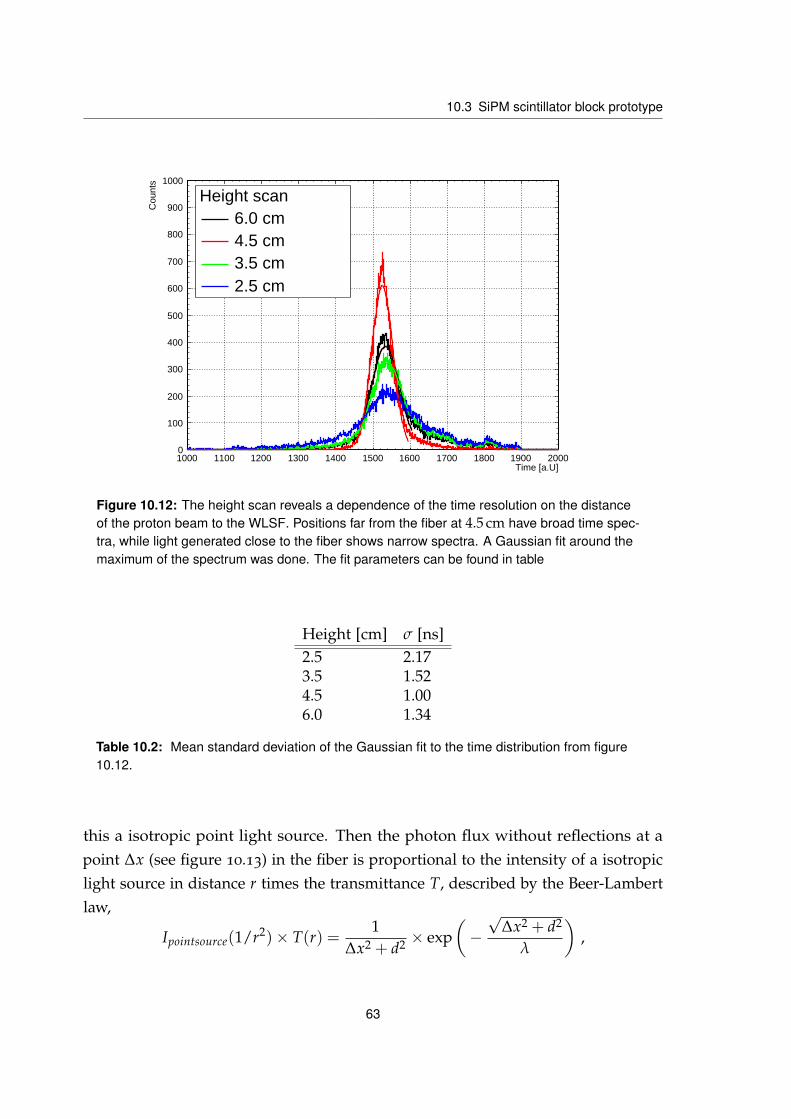
10.3 SiPM scintillator block prototype
Time [a.U]1000 1100 1200 1300 1400 1500 1600 1700 1800 1900 2000
Cou
nts
0
100
200
300
400
500
600
700
800
900
1000
Height scan6.0 cm4.5 cm3.5 cm2.5 cm
Figure 10.12: The height scan reveals a dependence of the time resolution on the distanceof the proton beam to the WLSF. Positions far from the fiber at 4.5 cm have broad time spec-tra, while light generated close to the fiber shows narrow spectra. A Gaussian fit around themaximum of the spectrum was done. The fit parameters can be found in table
Height [cm] σ [ns]2.5 2.173.5 1.524.5 1.006.0 1.34
Table 10.2: Mean standard deviation of the Gaussian fit to the time distribution from figure10.12.
this a isotropic point light source. Then the photon flux without reflections at apoint ∆x (see figure 10.13) in the fiber is proportional to the intensity of a isotropiclight source in distance r times the transmittance T, described by the Beer-Lambertlaw,
Ipointsource(1/r2)× T(r) =1
∆x2 + d2 × exp(−√
∆x2 + d2
λ
),
63

10 Tests on the time resolution and readout system
where lambda is the absorption length of the material, d the distance of the pointsource from the fiber, ∆x the parallel component of the distance of the light sourceto a point on the fiber in figure 10.13. For reflected light the source appears tohave a greater distance from the fiber and the shape of the distribution does notchange. This contribution to the spectrum decreases rapidly with the number ofreflections. Also the time for photons to reach the fiber increases with the numberof reflections. A trigger is produced if the number of photons hitting both SiPMwithin the coincidence time is greater than a certain threshold. This indicatesthat the measured spectrum is a combination of the initial light and the photonabsorption and reemission in the fiber and a smaller contribution from reflectedlight. This may be the reason why broadening occurs rapidly, when d increases.A slight asymmetry in the spectrum may be caused due to the low light output,which means that for one side less triggers are generated, in case the SiPM-fibercoupling is different.
WLSF
r (P
hoto
n)
d
Δx
Isotropic light source(Bragg peak)
Figure 10.13: A sketch for emission of a point source and the photon absorption by a thin fiber.
Figure 10.14 shows the time spectra at different x positions along the scintillatorat height 4.5 cm, figure 10.15 at height 2.5 cm. For analysis a Gaussian fit was donearound a region of interest symmetric to the maximum. One finds a plot for ∆t,as time difference of the converted Gaussian mean values, versus the positions infigure 10.17. From figure 10.17 via fit of a linear function one obtains an effectivevelocity of light (see table 10.3), which is comparable to the velocity of light in theBCF-12 fiber, but consists of two components. One is originated in the way of lightin the scintillator, while the other component is due to the geometry of the WLSF.
64

10.3 SiPM scintillator block prototype
Time [a.U]1000 1100 1200 1300 1400 1500 1600 1700 1800 1900 2000
Cou
nts
0
100
200
300
400
500
60055.00_cm45.00_cm35.00_cm25.00_cm15.00_cm5.00_cm
Figure 10.14: The time spectra for different x-positions at a height of 4.5 cm near the WLSF.For analysis a Gaussian was fit in a range symmetric to the maximum.
10.3.2 Direct readout of scintillator SiPM2/4
One idea to improve the position resolution obtained via the time distribution ofthe signals is to use two SiPMs coupled directly to the scintillator. The obtainedtime spectra one finds in figure 10.16. Characteristic for these spectra is that theyhave a broad background and a small peak, which results from the reflected directlight component. The effective velocity of light (see figure 10.17) is smaller thanwith the SiPM fiber coupling configuration, which is probably an effect of the highprobability that multiply reflected light triggers the SiPM. In figure 10.18 a typicalspectrum for the direct coupling can be seen. The problem of this method is, thatthe peak consists of very few events, which is due to a bad detector efficiency. Thisrules out the direct coupling option as detector concept.
65

10 Tests on the time resolution and readout system
Time [a.U]1000 1100 1200 1300 1400 1500 1600 1700 1800 1900 2000
Cou
nts
0
50
100
150
200
250
300
35055.00_cm
45.00_cm
35.00_cm
25.00_cm
15.00_cm
5.00_cm
Figure 10.15: The time spectra for different x-positions at a height of 2.5 cm, far from theWLSF. The distributions are broader because of geometrical effects.
Sample ce f f [cm ns−1] Spat. res (σ) [cm]Fiber readout h = 4.5cm 8.01± 0.01 10Fiber readout h = 2.5cm 8.98± 0.03 16Direct readout h = 2.5cm 5.38± 0.02 10
Table 10.3: The obtained effective velocities of light and the mean width of the Gaussian fitfunction in units of cm. Note that the real error on the ce f f is underestimated.
66

10.3 SiPM scintillator block prototype
Time [a.U]1000 1100 1200 1300 1400 1500 1600 1700 1800 1900 2000
Cou
nts
0
50
100
150
200
250 25.00_cm30.00_cm35.00_cm40.00_cm45.00_cm50.00_cm55.00_cm
Figure 10.16: The time distribution spectra for direct coupling of two Ham. 3x3 050C to thescintillator. A broad background due to the low light output is visible.
pos [cm]0 10 20 30 40 50 60
t [s
]
-10
-8
-6
-4
-2
0
-910×
WLSF readout height 2.5 cm
WLSF readout height 4.5 cm
direct readout height 2.5 cm
Figure 10.17: The position of the mean values obtained by the Gaussian fit to the region ofinterest symmetric to the maximum value of the time spectrum. The error bars are the fit errorson the mean of the Gaussian, which probably underestimate the true error.
67
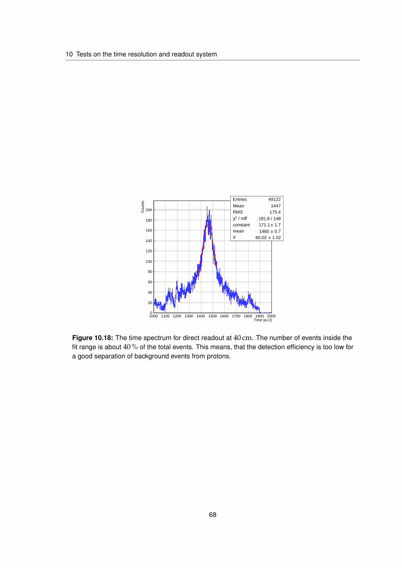
10 Tests on the time resolution and readout system
Time [a.U]1000 1100 1200 1300 1400 1500 1600 1700 1800 1900 2000
Cou
nts
0
20
40
60
80
100
120
140
160
180
200
Entries 49122
Mean 1447RMS 175.4
/ ndf 2χ 181.8 / 148constant 1.7± 171.1 mean 0.7± 1460
σ 1.02± 60.02
Figure 10.18: The time spectrum for direct readout at 40 cm. The number of events inside thefit range is about 40 % of the total events. This means, that the detection efficiency is too low fora good separation of background events from protons.
68

CHAPTER 11
Conclusion and outlook
The goal of this work was the optimization of a fast scintillation detector for a largeareas with SiPM readout and trigger capability. The detector consists ofBC-400
scintillator rods, BCF-92 fibers glued to the scintillator. The light emitted at the endof the fiber is collected with SiPMs.
This work consists of two parts. In the first part different SiPM types were char-acterized. For the latter a temperature controlled (0.1 K) test setup was developed,which was used for automatically determining Vbd, dG/dV, dVbd/dT and Rquench.Via a the forward U-I scan the microcell resistance Rquench has been measured for 5
different SiPM types. For the reverse U-I scan the breakdown voltage of differentSiPM types was reconstructed using a linear-quadratic function. Temperaturestudies were performed to determine the temperature coefficient via this method.The parameters dG/dV, dVbd/dT and Vbd have been measured automatically, illu-minating the SiPM with a pulsed LED. The charge contained in the signal pulse wasrecorded at different voltages and charge spectra were generated. A multigaussianfit function was used to describe the spectrum and in this way Vbd was measuredat high precision with an error of 64 mV. From the position of single pixel peaks atdifferent bias voltages dG/dV is obtained. These parameters have been determinedfor about 30 SiPMs of different form factors and microcell sizes. dG/dV is largestfor the SiPMs with 100 µm cell size and smallest for 25 µm cells, which puts anupper limit for the accuracy of the voltage source. The determination of Vbd wasnecessary, because the vendor only gives a recommended bias voltage, which isgreater than Vbd. Measurements with the POSSUMUS prototypes had shown, thatthe low light output was the main issue in order to improve the position resolution.
69

11 Conclusion and outlook
The decision was made to use SiPMs with microcell size of 100 µm× 100 µm, be-cause of their greater photon detection efficiency. For this SiPM type a temperaturecoefficient dVbd/dT of 60 mV K−1 was measured, which is in good accordance tothe obtained value via the U-I method.
Due to temperature fluctuations in the laboratory it was important to build asystem, that reduces the effects of gain variation. For this purpose the automaticmultichannel SiPM gain stabilization system has been developed, which minimizesthe gain variation due to temperature dependence of Vbd. This system relies on theinput of the temperature sensor mounted to the SiPM board and corrects the biasvoltage according to the measured temperature coefficient. The circuit is based ona digital controlled voltage divider. The gain could be stabilized within 0.92 % andno long term drifts were visible.
In order to understand the effect of crosstalk on the distribution of the number offiring microcells a simple Monte Carlo detector response model has been developed.The model contains no information on the microcell structure and is thereforeapplicable to a wide range of SiPM types. Comparison with data shows sensibleresults, indicating, that the Poisson assumption for the number of incoming photonsis good. The model includes crosstalk and afterpulsing effects and the photondetection efficiency. In the range from 0 to 3 firing microcells one finds the largestdeviations of the simulated data from the measured spectrum, which may be aneffect of dark counts, which have not been included in the model.
In the second part of this work studies on the position sensitivity along thelong side of a POSSUMUS prototype were done. For this purpose three detectorprototypes were built, which were tested with a 5 mm, 20 MeV proton beam at theMLL-Garching. Two prototypes are based on a 5 mm diameter BCF-12 scintillatingfiber and were used to test the timing capabilities of the readout system and theused SiPMs. One of those prototypes was coupled to conventional photomultipliers,the other one to Ham. 3x3 100C SiPMs. Time spectra were recorded and from theseone obtains a position resolution of 1.8 cm for photomultipliers, 2.86 cm for SiPMreadout.
The POSSUMUS prototype consists of a 60 cm long, 4 cm× 9 cm rectangularscintillator with a 1 mm BCF-92 fiber glued centered, parallel to the x-axis, whichcorresponds to the long side of the scintillator. The POSSUMUS prototype wasscanned with the proton beam along the y-axis and the time spectra show, that
70

the position resolution via the time information depends on the distance from theproton beam to the fiber. The Gaussian width of the time distribution near the fiberwas measured to be 1 ns and decreases rapidly with the distance to the fiber.
From a scan along the 0.6 m long side of the scintillator rod one obtains a meanposition resolution of 10 cm near the fiber and 16 cm at a distance of 2 cm parallelto the fiber. For direct readout with two SiPMs centered to the 9 cm× 4 cm surfaceof the scintillator, the position resolution is 10 cm but the detection efficiency istoo bad to consider this an improvement of the detector. The limiting factor in thetime measurement is the transit time jitter of the photons in the scintillator, whileelectronic effects, scintillation process and electronic noise play a minor role. Thisindicates, that for obtaining a position resolution of 10 cm along the x-Axis, othermethods of analysis e.g. combining pulse height and timing information, must beconsidered or other scintillator geometries should be tested.
Further improvements of the position sensitivity along the long side of thedetector may be achieved by adding more fibers to the detector such, that thespacing between the fibers is about 1 cm or less. Furthermore for better lightcollection a Winston cone like scintillator may be glued to the ends of the long sideor fiber couplers, which join several fibers together, could be used. SiPM readout ofeach cone will improves the SNR in contrast to direct readout of the flat scintillatorsurface and may have small effects on time information.
Considering the used SiPM the difficulty was to stabilize gain at high precision,because optical crosstalk puts an upper limit for the feasible Vover. Recent develop-ments of SiPM with reduced optical crosstalk can be biased at higher Vover, whichmay increase the photon detection efficiency, reduce the requirements for gain sta-bilization and extend the linearity of the detector response. The gain stabilizationsystem may be improved using a feedback signal, which is computed from theSiPM single pixel signal. A drawback of the current system is, that for gain moni-toring purpose the readout of high energetic events must be stopped. The detectoris operated by switching the discriminator thresholds between gain monitoringlevel using the dark rate and the level for signals from incoming particles. Forconstant gain monitoring a second high gain readout channel for each SiPM isrecommended, which uses the full dynamic range of the charge-to-digital converter(QDC).
71

11 Conclusion and outlook
This work has shown, that SiPMs are suited as a readout for the POSSUMUSdetector and that the detector principle has been proven. An automatic test setupwas used to characterize the SiPMs used for the detector. The goal of a positionresolution of 10 cm could not be achieved with the current detector prototypes,but the limiting effects are well-known and ways to improve the resolution werementioned.
72

APPENDIX A
Appendix
A.1 The Chi-Square Test for comparison of experimental and
simulated data
Wheighted histograms can be obtained from a Monte Carlo Simulation and experi-ment. Comparing data and the Monte-Carlo data one possibility to get an estimateof the goodness of the model is the Chi-Square Test, which shall be derived in thenext section. The following is a sketch of the Chi-Square method as presented inGagunashvili [2010]:
The probability for a random event to belong to bin i of a histogram with m binsis given by the integral over a region Si of the underlying PDF:
pi =∫Si
p(x)dx, i = 1,...,m (A.1)
A histogram with m bins states the result of a random experiment with the PDFp(x). The homogeneity hypothesis assumes that two histograms have identicalunderlying probability distributions, which is equivalent to:
1. ∑mi=1pi = 1
2. pi =probability for a measured value to belong to the ith bin
73

A Appendix
A.1.1 Unweighted histograms
Now define the total number of events in histogram j belonging to the ith-bin asnji and
Xj =m
∑i=1
(nij − nj pi)2
nj pij = 1,2 (A.2)
a random variable, which has a χ2m−1 distribution (see glossary Chisquare Distri-
bution), where the histogram number j is represented by j, because the ChisquareDistribution is the distribution of the sum of the squares of a number of inde-pendent standard normal random variables. Now for statistically independenthistograms:
2
∑j=1
Xj =2
∑j=1
m
∑i=1
(nij − nj pi)2
nj pi(A.3)
is approximately distributed as χ22m−2 and the probabilities p1,...,pm are obtained
by minimization of equation A.3.
One estimates pi by the following expression:
pi =n1i + n2i
n1 + n2(A.4)
Substitute A.4 in A.3 one obtains:
2
∑j=1
m
∑i=1
(nij − nj pi)2
nj pi=
1n1n2
m
∑i=1
(n2n1i − n1n2i)2
n1i + n2i(A.5)
Where the expression in A.5 is χ2m−1 distributed with estimation of m− 1 param-
eters.
A.1.2 Weighted histograms
In analogy for weighted histograms we define
pi =∫Si
p(x)dx =∫Si
w(x)p(x)dx (A.6)
74

A.1 The Chi-Square Test for comparison of experimental and simulated data
as the integral in a given region of the product of a weight function
w(x) = p(x)/g(x) (A.7)
and p(x), where g(x) is an abritrary PDF. Further it holds:
g(x) > 0 ∀x ∈ X = x : p(x) 6= 0w(x) = 0 ∀x ∈ Y = x : p(x) = 0
(A.8)
Define normalized weights as w(x) and in analogy unnormalized weights:
w(x) = const · w(x) (A.9)
The sum of weights is given by:
Wi =ni
∑k=1
wi(k) (A.10)
ni number of events in bin i and wi weight of kth event in the ith bin. So that thetotal number of events in the histogram is given by n = ∑m
i=1 ni
To do the test of homogeneity we define the statistics:
X2h =
m
∑i=1
(W1i −W2i)2
d2i
(A.11)
With Wij as the sum of weights of the ith bin of jth histogram and s2(Wij) as totalsum of squares of the weights in the ith bin of the jth histogram.
di =
W2i[s2(W1i)/W1i + s2(W2i)/W2i] n1 ≤ n2
W1i[s2(W1i)/W1i + s2(W2i)/W2i] n2 < n1
(A.12)
According to [Gagunashvili, 2010, p.5] X2h has a chi-square distribution.
75

A Appendix
A.1.3 Histograms with normalized weights
For two histograms with normalized weights the total sum of weights of events Wij
in the ith bin of the jth histogram is given by
Wij =
nij
∑k=1
wij(k) (A.13)
and nij, wij are independent random variables. We introduce a variable
rji = Ewij/Ew2ij (A.14)
as the ratio of first to second moment of the distribution of weights in bin i. Thecalculation of the test statistic yields [see p. 7 Gagunashvili, 2010]:
X2k =
2
∑j=1
1nj
∑i 6=k
rjiW2ji
pi+
2
∑j=1
1nj
(nj −∑i 6=k rjiWji)2
1−∑i 6=k rji pi−
2
∑j=1
nj (A.15)
where
rji =
nij
∑k=1
wij(k)/nij
∑k=1
w2ij(k) (A.16)
and withpi =
r1iW1i + r2iW2i
r1in1r2in2(A.17)
as initial approximation for pi. Numerically one minimizes (A.15) and in this waywe obtain the estimators for the probabilities pi.
A.2 The constant fraction triggering technique
Time measurements of electrical signals at high precision are challenging and it isimportant to find trigger criteria independent of the pulseheight. For this reasonthe Constant Fraction Triggering was introduced and up to now this method oftriggering is one of the most important and versatile method to measure time.
This method avoids timewalk due to a variance in signalheight, but requiresconstant rise time for the signal [Leo, 1994, see pp. 327]. A signal is split into two.One part is delayed, whereas the other part is attenuated by a factor k and inverted.
76

A.3 Uniformity of channels for the voltage divider
Now the sum of this signals has a zero-crossing point at a constant fraction k of theoriginal signal, which can be used for a trigger logic signal.
If the delay time is so short and the undelayed signal does not reach its peak, thenonly the first component of the signal is taken into account for the calculation of thezero crossing point, the technique is called amplitude and risetime compensationtriggering, which is suited for SiPM signal and cancels the effects of afterpulses.Additionally a deadtime in the order of the signal length inhibits further triggers.
time [a.U]0 20 40 60 80 100
volta
ge [a
.U.]
-0.4
-0.2
0
0.2
0.4
0.6
0.8
Figure A.1: When the signals of differentamplitudes exceed a constant threshold atrigger signal is generated. Signal 1 triggersbefore Signal 2. This time difference is calledwalk
time [a.U]0 20 40 60 80 100
volta
ge [a
.U.]
-0.4
-0.2
0
0.2
0.4
0.6
0.8
Figure A.2: The Constant Fraction Triggeringeliminates walk, when the original Signal isdelayed and a split Signal is inverted andattenuated by a factor k. The sum Signaldefines the trigger at the zero crossing point.
A.3 Uniformity of channels for the voltage divider
The calibration measurements for the voltage divider without electrical load as infigure 8.1 were done using a Keithley 6514 Electrometer, to check the uniformity ofchannels and to get the parameters for a more accurate adjustment of the outputvoltage. The obtained general values for all channels are 0.01857 V per RDAC valueand 0.281 V offset. These are results of fitting a constant (see figure A.5).
77

A Appendix
RDAC-val0 50 100 150 200 250
U [V
]
1
2
3
4
5
Figure A.3: The output voltage vs the set8 bit RDAC-Value for 24 channels. Viastraight line fit one obtains the parametersfor offset and slope.
RDAC-val0 50 100 150 200 250
devi
atio
n [V
]
-0.025
-0.02
-0.015
-0.01
-0.005
0
loadR 600 kOhm 800 kOhm 1000 kOhm 1200 kOhm 1400 kOhm
Figure A.4: The simulated deviation fromthe set voltage for the 20 kΩ digital voltagedivider for 5 V for different load resistances.
Channel No0 5 10 15 20 25
slop
e [V
/RD
AC
_val
]
18.56
18.565
18.57
18.575
18.58
-310×p0 2.039e-07± 0.01857 p0 2.039e-07± 0.01857
Channel No0 5 10 15 20 25
Offs
et [V
]
0.28
0.28020.28040.28060.2808
0.2810.2812
0.28140.28160.2818 p0 1.083e-05± 0.281 p0 1.083e-05± 0.281
Figure A.5: The fit parameters from figure A.3.
78

A.3 Uniformity of channels for the voltage dividerSi
PMN
oSe
rial
Form
atTy
peG
ate
[ns]
T mea
s[K
]V
bdV
bd(T
=25
K)
dG
/dV
Erro
rd
G/
dV11
1641
1x1
100
45
20
69.2
869.5
81.
15×
106
1.75×
104
11
1641
1x1
100
35
20
69.2
869.5
89.
50×
105
3.74×
104
40
k000863
3x3
100
45
20
71.0
171.3
17.
56×
105
1.27×
104
45
2k0
0856
3x3
100
45
20
70.9
271.2
26.
66×
105
1.71×
103
44
2k0
00854
3x3
100
45
20
71.0
271.3
28.
02×
105
2.20×
104
39
2k0
00860
3x3
100
45
20
71.0
871.3
87.
81×
105
2.01×
104
61644
1x1
100
45
20
69.3
069.6
01.
21×
106
5.68×
104
11
1641
1x1
100
45
20
69.2
869.5
81.
15×
106
2.24×
104
47
1643
1x1
100
45
20
69.3
169.6
11.
21×
106
3.18×
104
48
2628
1x1
100
45
20
69.2
569.5
51.
28×
106
3.03×
104
49
2630
1x1
100
45
20
69.4
369.7
31.
30×
106
3.48×
104
51
2626
1x1
100
45
20
69.2
169.5
11.
28×
106
3.56×
104
52
2634
1x1
100
45
20
69.4
869.7
81.
27×
106
3.04×
104
54
2635
1x1
100
45
20
69.4
669.7
61.
27×
106
5.65×
104
50
2627
1x1
100
45
20
69.2
469.5
41.
23×
106
3.04×
104
36
2j0
06433
3x3
50
45
25.4
72.4
272.4
01.
33×
106
6.44×
104
34
2k0
00851
3x3
100
45
25
71.2
971.2
98.
10×
105
3.70×
104
58
2j0
0064272
3x3
100
45
26.1
70.9
770.9
07.
87×
105
1.57×
103
41
2k0
00859
3x3
100
45
26
71.3
771.3
18.
35×
105
6.04×
104
55
2k0
00845
3x3
100
45
26
71.6
071.5
47.
75×
105
2.74×
104
46
2k0
00855
3x3
100
45
25.8
71.3
171.2
68.
08×
105
2.73×
104
57
2j0
006432
3x3
50
45
25.8
71.1
071.0
53.
45×
105
9.36×
103
53
2633
1x1
100
45
25
69.8
269.8
21.
22×
106
3.46×
104
42
2k0
00861
3x3
100
45
26.2
71.3
471.2
71.
02×
106
3.75×
104
32
2k0
00xx
x3x3
100
45
27.1
71.5
171.3
81.
03×
106
4.23×
104
43
2k0
00802
3x3
100
45
26.8
71.4
371.3
28.
55×
105
3.96×
104
Tabl
eA
.1:
The
valu
esfo
rVbd
and
dG
/dV
fort
heS
iPM
sus
edin
the
PO
SS
UM
US
prot
otyp
es.
79
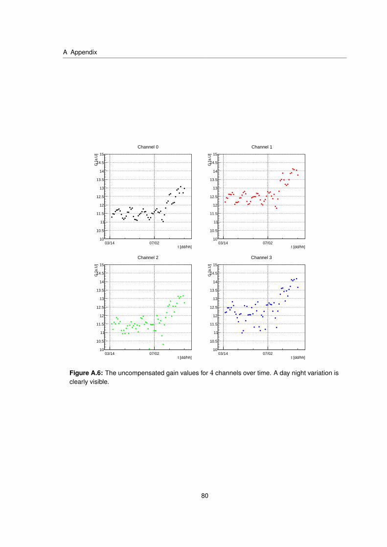
A Appendix
t [dd/hh]03/14 07/02
G [a
.U]
10
10.5
11
11.5
12
12.5
13
13.5
14
14.5
15
Channel 0
t [dd/hh]03/14 07/02
G [a
.U]
10
10.5
11
11.5
12
12.5
13
13.5
14
14.5
15
Channel 1
t [dd/hh]03/14 07/02
G [a
.U]
10
10.5
11
11.5
12
12.5
13
13.5
14
14.5
15
Channel 2
t [dd/hh]03/14 07/02
G [a
.U]
10
10.5
11
11.5
12
12.5
13
13.5
14
14.5
15
Channel 3
Figure A.6: The uncompensated gain values for 4 channels over time. A day night variation isclearly visible.
80

A.3 Uniformity of channels for the voltage divider
t [dd/hh]11/06 12/09 13/12 14/15 15/18 16/21
G [a
.U]
10
10.5
11
11.5
12
12.5
13
13.5
14
14.5
15
Channel 0
t [dd/hh]11/06 12/09 13/12 14/15 15/18 16/21
G [a
.U]
10
10.5
11
11.5
12
12.5
13
13.5
14
14.5
15
Channel 1
t [dd/hh]11/06 12/09 13/12 14/15 15/18 16/21
G [a
.U]
10
10.5
11
11.5
12
12.5
13
13.5
14
14.5
15
Channel 2
t [dd/hh]11/06 12/09 13/12 14/15 15/18 16/21
G [a
.U]
10
10.5
11
11.5
12
12.5
13
13.5
14
14.5
15
Channel 3
Figure A.7: The compensated gain values for 4 channels.
81

A Appendix
Figure A.8: The wiring diagram for the H bridge used to change the direction of the Peltierelement current. The direction of the current can be set via the RTS-line of a RS232 interface.
82
Bibliography
Pietro P Altermatt, Andreas Schenk, Frank Geelhaar, and Gernot Heiser. Reassess-ment of the intrinsic carrier density in crystalline silicon in view of band-gapnarrowing. Journal of Applied Physics, 93(3):1598–1604, 2003. (Cited on page 5)
Elektronik Automatik. Datasheet EA-PSI 8160-04 t, 2014. URL http://www.
elektroautomatik.de/. (Cited on page 57)
O Biebel, M Binder, M Boutemeur, A Brandt, J Dubbert, G Duckeck, J Elmsheuser,F Fiedler, R Hertenberger, and O Kortner. A cosmic ray measurement facilityfor ATLAS muon chambers. arXiv preprint physics/0307147, 2003. URL http:
//arxiv.org/abs/physics/0307147v1. (Cited on page 1)
Andreas Bollu. Characterisation of silicon-photomultiplier noise and optimi-sation of light detection through coupling with optical fibres, April 2014.(Cited on page 48)
P. Buzhan, B. Dolgoshein, L. Filatov, A. Ilyin, V. Kantzerov, V. Kaplin,A. Karakash, F. Kayumov, S. Klemin, E. Popova, and S. Smirnov. Sili-con photomultiplier and its possible applications. Nuclear Instruments andMethods in Physics Research Section A: Accelerators, Spectrometers, Detectorsand Associated Equipment, 504(1-3):48–52, May 2003. ISSN 01689002. doi:10.1016/S0168-9002(03)00749-6. URL http://linkinghub.elsevier.com/
retrieve/pii/S0168900203007496. (Cited on pages 13 and 14)
Caen. Datasheet n455 logic, October 2004. URL http://www.caen.it/.(Cited on page 55)
Caen. Datasheet v792 QDC, 2010. URL http://www.caen.it/.(Cited on page 35)
83

Bibliography
Caen. Datasheet DS2477 LED driver, 2011a. URL http://www.caen.it/.(Cited on page 35)
Caen. Datasheet n845 LTD, May 2011b. URL http://www.caen.it/.(Cited on page 55)
Caen. Datasheet v775n TDC, December 2012. URL http://www.caen.it/.(Cited on page 55)
David L. Chichester, Scott M. Watson, and James T. Johnson. Comparison ofBCF-10, BCF-12, and BCF-20 scintillating fibers for use in a 1-dimensional linearsensor. In Comparison of BCF-10, BCF-12, and BCF-20 scintillating fibers for usein a 1-dimensional linear sensor, pages 365–370. IEEE, October 2012. ISBN 978-1-4673-2030-6, 978-1-4673-2028-3, 978-1-4673-2029-0. doi: 10.1109/NSSMIC.2012.6551127. URL http://ieeexplore.ieee.org/lpdocs/epic03/wrapper.
htm?arnumber=6551127. (Cited on page 56)
F Corsi, C Marzocca, A Perrotta, A Dragone, M Foresta, A Del Guerra, S Marcatili,G Llosa, G Collazzuol, G-F Dalla Betta, and others. Electrical characterization ofsilicon photo-multiplier detectors for optimal front-end design. In Nuclear ScienceSymposium Conference Record, 2006. IEEE, volume 2, pages 1276–1280. IEEE, 2006.(Cited on page 18)
C. R. Crowell. TEMPERATURE DEPENDENCE OF AVALANCHE MUL-TIPLICATION IN SEMICONDUCTORS. Applied Physics Letters, 9(6):242,1966. ISSN 00036951. doi: 10.1063/1.1754731. URL http://scitation.
aip.org/content/aip/journal/apl/9/6/10.1063/1.1754731.(Cited on page 40)
Hermann Diels and Walther Kranz. Die Fragmente der Vorsokratiker griechisch unddeutsch, volume 2. Weidmannsche Buchhandlung, Berlin-Charlottenburg, 4
edition, 1922. (Cited on page )
N. Dinu, Z. Amara, C. Bazin, V. Chaumat, C. Cheikali, G. Guilhem, V. Puill,C. Sylvia, and J.F. Vagnucci. Electro-optical characterization of SiPM: A compara-tive study. Nuclear Instruments and Methods in Physics Research Section A: Accelera-tors, Spectrometers, Detectors and Associated Equipment, 610(1):423–426, October 2009.
84

Bibliography
ISSN 01689002. doi: 10.1016/j.nima.2009.05.101. URL http://linkinghub.
elsevier.com/retrieve/pii/S0168900209011383. (Cited on page 17)
Nicoleta Dinu. Instrumentation on Silicon Detectors: from properties char-acterization to applications. PhD thesis, Université Paris Sud-Paris XI,2013. URL http://hal.in2p3.fr/docs/00/87/23/18/PDF/HDR_Dinu.
pdf. (Cited on pages 16, 31, 33, and 49)
Patrick Eckert, Hans-Christian Schultz-Coulon, Wei Shen, Rainer Stamen, andAlexander Tadday. Characterisation studies of silicon photomultipliers. NuclearInstruments and Methods in Physics Research Section A: Accelerators, Spectrometers,Detectors and Associated Equipment, 620(2-3):217–226, August 2010. ISSN 01689002.doi: 10.1016/j.nima.2010.03.169. URL http://linkinghub.elsevier.com/
retrieve/pii/S0168900210008156. (Cited on page 47)
Tim Enzweiler. Development of a Multipurpose Light Source for SiPM Characterization.PhD thesis, RWTH Aachen, Aachen, November 2013. (Cited on page 49)
Paolo Finocchiaro, Alfio Pappalardo, Luigi Cosentino, Massimiliano Bel-luso, Sergio Billotta, Giovanni Bonanno, and Salvatore Di Mauro. Fea-tures of silicon photo multipliers: Precision measurements of noise, cross-talk, afterpulsing, detection efficiency. IEEE Transactions on Nuclear Sci-ence, 56(3):1033–1041, June 2009. ISSN 0018-9499. doi: 10.1109/TNS.2009.2014308. URL http://ieeexplore.ieee.org/lpdocs/epic03/wrapper.
htm?arnumber=5076065. (Cited on pages 18 and 47)
N.D. Gagunashvili. Chi-square tests for comparing weighted histograms. NuclearInstruments and Methods in Physics Research Section A: Accelerators, Spectrometers,Detectors and Associated Equipment, 614(2):287–296, March 2010. ISSN 01689002.doi: 10.1016/j.nima.2009.12.037. URL http://linkinghub.elsevier.com/
retrieve/pii/S0168900209023547. (Cited on pages 73, 75, and 76)
Benjamin Glauß. Optical Test Stand and SiPM characterisation studies. PhD thesis,RWTH Aachen, Aachen, May 2012. (Cited on page 49)
V. Golovin and V. Saveliev. Novel type of avalanche photodetector withgeiger mode operation. Nuclear Instruments and Methods in Physics Re-
85

Bibliography
search Section A: Accelerators, Spectrometers, Detectors and Associated Equip-ment, 518(1-2):560–564, February 2004. ISSN 01689002. doi: 10.1016/j.nima.2003.11.085. URL http://linkinghub.elsevier.com/retrieve/pii/
S0168900203029528. (Cited on page 13)
Martin A. Green. Self-consistent optical parameters of intrinsic silicon at 300kincluding temperature coefficients. Solar Energy Materials and Solar Cells,92(11):1305–1310, November 2008. ISSN 09270248. doi: 10.1016/j.solmat.2008.06.009. URL http://linkinghub.elsevier.com/retrieve/pii/
S0927024808002158. (Cited on page 7)
Johannes Grossmann. Charakterisierung von silizium-photomultipliern, July 2012.(Cited on page 20)
Roland H. Haitz. Model for the electrical behavior of a microplasma. Jour-nal of Applied Physics, 35(5):1370, 1964. ISSN 00218979. doi: 10.1063/1.1713636. URL http://scitation.aip.org/content/aip/journal/jap/
35/5/10.1063/1.1713636. (Cited on page 13)
ISEG. Datasheet ISEG SHQ 224m, February 2014. URL http://www.iseg-hv.
com. (Cited on page 54)
Keithley. Datasheet 2440 SourceMeter, 2002. URL http://www.keithley.com.(Cited on pages 30 and 37)
Keithley. Datasheet 6514 electrometer, 2003. URL http://www.keithley.com.(Cited on page 31)
Charles Kittel and Paul McEuen. Introduction to solid state physics, volume 8. WileyNew York, 1976. ISBN 0-471-41526-X. (Cited on pages 6, 7, and 8)
A.L. Lacaita, F. Zappa, S. Bigliardi, and M. Manfredi. On the bremsstrahlungorigin of hot-carrier-induced photons in silicon devices. IEEE Transactions onElectron Devices, 40(3):577–582, March 1993. ISSN 00189383. doi: 10.1109/16.199363. URL http://ieeexplore.ieee.org/lpdocs/epic03/wrapper.
htm?arnumber=199363. (Cited on page 19)
86

Bibliography
William R. Leo. Techniques for nuclear and particle physics experiments: a how-toapproach. Springer, Berlin ; New York, 2nd rev. ed edition, 1994. ISBN 3540572805.(Cited on pages 10, 12, 21, 22, and 76)
R. J. McIntyre. Theory of microplasma instability in silicon. Journalof Applied Physics, 32(6):983, 1961. ISSN 00218979. doi: 10.1063/1.1736199. URL http://scitation.aip.org/content/aip/journal/jap/
32/6/10.1063/1.1736199. (Cited on page 13)
Y. Musienko, S. Reucroft, and J. Swain. A simple model of EG&greverse reach-through APDs. Nuclear Instruments and Methods in PhysicsResearch Section A: Accelerators, Spectrometers, Detectors and AssociatedEquipment, 442(1-3):179–186, March 2000. ISSN 01689002. doi: 10.1016/S0168-9002(99)01218-8. URL http://linkinghub.elsevier.com/
retrieve/pii/S0168900299012188. (Cited on page 16)
Ralph Müller. Development of a position sensitive scintillating muon detector withsilicon photo-multiplier readout, September 2013. (Cited on page 26)
NIST. NIST PSTAR database, 2014. URL http://physics.nist.gov/
PhysRefData/Star/Text/PSTAR.html. (Cited on page 53)
Nepomuk Otte. Observation of VHE gamma–Rays from the Vicinity of magne-tized Neutron Stars and Development of new Photon-Detectors for Future Groundbased gamma–Ray Detectors. PhD thesis, TU München, München, August 2007.(Cited on page 49)
Kolja Prothmann. Comparative Measurements of Silicon Photomultipliers for the Read-out of a Highly Granular Hadronic Calorimeter. PhD thesis, Ludwig-MaximiliansUniversität, München, September 2008. (Cited on pages 35, 38, and 40)
Jozef Pulko. A Monte-Carlo Model of a Silicon Photomultiplier. PhD thesis, TechnischeUniversität München, München, December 2012. URL http://mediatum.ub.
tum.de/doc/1119328/1119328.pdf. (Cited on page 17)
Marco Ramilli. Characterization of SiPM: temperature dependencies. In NuclearScience Symposium Conference Record, 2008. NSS’08. IEEE, pages 2467–2470. IEEE,2008. (Cited on page 47)
87

Bibliography
Marco Ramilli, Alessia Allevi, Valery Chmill, Maria Bondani, Massimo Caccia, andAlessandra Andreoni. Photon-number statistics with silicon photomultipliers.JOSA B, 27(5):852–862, 2010. (Cited on pages 19 and 47)
D Renker and E Lorenz. Advances in solid state photon detectors. Journal ofInstrumentation, 4(04):P04004–P04004, April 2009. ISSN 1748-0221. doi: 10.1088/1748-0221/4/04/P04004. URL http://stacks.iop.org/1748-0221/4/
i=04/a=P04004?key=crossref.0b2aaff32d46c072c53ee73cbf621d59.(Cited on pages 15, 19, and 20)
Alexander Ruschke. Possumus. PhD thesis, Ludwig-Maximilians Universität,München, October 2014. (Cited on pages 1, 25, 26, 46, and 61)
Saint-Gobain_Crystals. Datasheet BCF-12, 2014a. (Cited on page 53)
Saint-Gobain_Crystals. Datasheet BCF-92,BC400, 2014b. URL http:
//www.crystals.saint-gobain.com/Plastic_Scintillation.aspx.(Cited on page 61)
MALVIN CARL Teich and BEA Saleh. Fundamentals of photonics. Canada, WileyInterscience, page 3, 1991. (Cited on page 47)
Voltcraft. Datasheet PSP 12010, 2008. URL http://www.produktinfo.conrad.
com/datenblaetter/500000-524999/512410-an-01-ml-PROGRAM_
SCHALTNETZTEIL_PSP_de_en_fr_nl.pdf. (Cited on page 28)
Wacker. Datasheet wacker AK 500 000, June 2013. URL http://www.wacker.com.(Cited on page 57)
T.O. White. Scintillating fibres. Nuclear Instruments and Methods inPhysics Research Section A: Accelerators, Spectrometers, Detectors and Associ-ated Equipment, 273(2-3):820–825, December 1988. ISSN 01689002. doi:10.1016/0168-9002(88)90102-7. URL http://linkinghub.elsevier.com/
retrieve/pii/0168900288901027. (Cited on pages 22 and 24)
F. Zappa, S. Tisa, A. Tosi, and S. Cova. Principles and features of single-photonavalanche diode arrays. Sensors and Actuators A: Physical, 140(1):103–112, October
88

Bibliography
2007. ISSN 09244247. doi: 10.1016/j.sna.2007.06.021. URL http://linkinghub.
elsevier.com/retrieve/pii/S0924424707004967. (Cited on page 19)
89


Acronyms
Vover overvoltage
AP afterpulseAPD Avalanche Photo Diode
CFD constant fraction discriminatorCRF Cosmic Ray FacilityCWG Clear Wave Guide
DCR Dark Count RateDS18B20 DS18B20 temperature sensor
ENF Excess Noise Factor
GM-APD Geiger mode APD
Ham. 1x1 025C Hamamatsu S10362-11-025CHam. 1x1 050C Hamamatsu S10362-11-050CHam. 1x1 100C Hamamatsu S10362-11-100CHam. 3x3 025C Hamamatsu S10362-3x3-025CHam. 3x3 050C Hamamatsu S10362-3x3-050CHam. 3x3 100C Hamamatsu S10362-3x3-100C
OC Optical Crosstalk
91

Acronyms
PDE Photon Detection EfficiencyPDF Probability Density FunctionPE photo electronpsp1210 PSP1210 Voltcraft programable power supplyPWM Pulse-width modulation
QDC charge-to-digital converter
SiPM Silicon PhotomultiplierSNR signal-to-noise-ratio
TDC time-to-digital converter
WLSF wavelength shifting fiber
92

Symbols
CCell The capacitance of the a SiPM microcellEF The Fermi energy.G The amount of charge contained in an avalanche
discharge of a single microcell divided by eIbulk The current, that flows through the bulk of a p-
n junction and eventually is subject to avalanchemultiplication
QE The quantum efficiency to create an electron-holepair.
RD The diode equivalent resistance of a SiPM micro-cell
Rquench The quenching resistance of a SiPM microcellU The net number of charge carriers generated per
volume as difference between e-h pair generationand recombination rates. U = Rth − Gth
Vbd the breakdown voltage of a SiPMVbias the bias voltage of a SiPMVover Vover = Vbias −Vbd
Vt The terminal voltage of a voltage dividerα Charge carrier ionization probability per unit dis-
tance travelleddG/dV The temperature coefficient of the SiPM gaindVbd/dT The temperature coefficient of the breakdown volt-
age.
93

Symbols
εgeom The fill factor of a SiPM as ratio of optical activesurface to total detector area.
εi Ionization energyεr Raman optical phonon energyεtrigger The avalanche trigger probability for a single e-h
pair.λPoisson The mean value of a Poisson distribution.λ Carrier mean free path for optical phonon genera-
tionnc the number of microcell APDs on the SiPMntrigger the number of triggered microcells during a short
light pulse SiPMni The intrinsic density of charge carriers in thermal
equilibrium.pcross The crosstalk probability for one microcell to trig-
ger another microcellPDE The photon detection efficiency.τe The lifetime of an e-h-pair.
94

Glossary
amplitude and risetime compensation triggering
The difference to Constant Fraction Triggering triggering is the delay betweenthe inverted and attenuated signal. This technique has delays so short, thatit does not allow the undelayed signal to reach its peak and so only theearly portion of signal is taken into account for a trigger decision, which isespecially suited for a SiPM with afterpulses during microcell recovery.
BC-400
A fast plastic scintillator by St. Gobain.
BCF-12
A scintillating fibre with 3.2 ns decay time.
BCF-92
A 1.0 mm wave length shifting fiber with 2.7 ns decay time and peak emissionat 492 µm.
Chisquare Distribution
A special case of a PDF:
f (x;k) =
x(k/2−1)e−x/2
2k/2Γ( k2 )
, ∀x ≥ 0
0, otherwise(A.18)
Constant Fraction Triggering
A modern high precision method for triggering minimizing time walk effects.
95

Glossary
contact potential
In thermodynamic equilibrium the contact potential is the electrostatic poten-tial difference between two metals or semiconductors in contact close to thesurface of the boundary region.
depletion zone
The depletion zone is the boundary region between the n-type and p-typesemiconductor and is essentially free of mobile charge carriers.
Excess Noise Factor
The variation in charge given a constant signal for an APD in proportionalmodem arises due to randomness in photon arrivals and randomness incarrier multiplication process. For a SiPM the ENF is given by the 1-photonsignal
ENF = 1 + σ21 /S2
1 , (A.19)
where σ1 is the variance of the peak and S1 is the mean value of the peak.This indicates the pixel-to-pixel gain variation.
I2C Bus
A digital 2-wire Bus system for setting the RDAC values.
Monte Carlo Simulation
The Monte Carlo method is a way of obtaining the distribution of an unknownPDF relying on repeated random sampling.
p-n junction
The boundary region between p- and n-type semiconductors.
PID controller
The PID controller is a simple controlling algorithm, which uses a feedbacksignal. The PID controller is considered to be the best controller, if no
96

Glossary
information about the underlying process is given. The error e between theprocess variable and the set point e = SP− PV defines the controller output.
u(t) = KP(e(t) +1Ti
t∫0
e(τ)dτ + Tdddt
e(t)) (A.20)
Poisson distribution
The Poisson distribution defined as:
f (k,λ) =λkeλ
k!(A.21)
POSSUMUS
A Position Sensitive Scintillating Muon Detector with SiPM readout.
RDAC
A digitally controlled potentiometer.
walk
When coincident signals of different amplitudes cross a discriminator thresh-old at different times, the time difference is called time walk.
97


List of Figures
1.1 The CRF in Garching . . . . . . . . . . . . . . . . . . . . . . . . . . . . 2
3.1 Band structures . . . . . . . . . . . . . . . . . . . . . . . . . . . . . . . 6
3.2 Absorption coefficient of silicon . . . . . . . . . . . . . . . . . . . . . . 7
3.3 Doping for p-type and n-type silicon . . . . . . . . . . . . . . . . . . . 10
3.4 p-n junction . . . . . . . . . . . . . . . . . . . . . . . . . . . . . . . . . 11
3.5 Hamamatsu S10362-33-100C . . . . . . . . . . . . . . . . . . . . . . . . 14
3.6 Equivalent circuit diagram of a SiPM . . . . . . . . . . . . . . . . . . 14
3.7 SiPM doping concentrations and configuration of electric field . . . 15
3.8 Avalanche multiplication in Geiger mode . . . . . . . . . . . . . . . . 15
3.9 Operating mode for a GM-APD . . . . . . . . . . . . . . . . . . . . . . 16
3.10 Ionization coefficients for electrons and holes . . . . . . . . . . . . . . 16
3.11 The equivalent circuit for a SiPM at low photon flux . . . . . . . . . 18
3.12 Dark count rate versus voltage . . . . . . . . . . . . . . . . . . . . . . 20
4.1 Scintillation principle . . . . . . . . . . . . . . . . . . . . . . . . . . . . 22
5.1 Wavelength shifter principle . . . . . . . . . . . . . . . . . . . . . . . . 24
6.1 Sketch possumus . . . . . . . . . . . . . . . . . . . . . . . . . . . . . . 25
6.2 Basic principle of position sensitivity along y-axis . . . . . . . . . . . 26
7.1 Current voltage characteristic for 50 mm× 50 mm Peltier element . . 29
7.2 T vs time at controller setpoints . . . . . . . . . . . . . . . . . . . . . . 29
7.3 Setup for the measurement of U-I characteristic . . . . . . . . . . . . 31
7.4 Current voltage forward characteristic for different SiPM types . . . 31
7.5 Current voltage reverse characteristic for a Ham. 3x3 050C . . . . . . 33
99

List of Figures
7.6 The U-I characteristic for the tested SiPM types . . . . . . . . . . . . 33
7.7 Current voltage reverse characteristic for a Ham. 3x3 100C SiPM atdifferent temperatures . . . . . . . . . . . . . . . . . . . . . . . . . . . 34
7.8 The temperature coefficient of a Ham. 3x3 100C via U-I characteristic 35
7.9 Setup for SiPM characterization at low photon flux. . . . . . . . . . . 37
7.10 QDC-readout scheme . . . . . . . . . . . . . . . . . . . . . . . . . . . . 37
7.11 QDC spectrum of a Ham. 1x1 100C . . . . . . . . . . . . . . . . . . . 38
7.12 Peak positions for determination of Vbd . . . . . . . . . . . . . . . . . 39
7.13 Temperature coefficient dVbd/dT via charge spectra . . . . . . . . . . 40
8.1 The multichannel gain stabilization system . . . . . . . . . . . . . . . 44
8.2 The peaks of the charge distribution spectra at different temperaturesat constant bias . . . . . . . . . . . . . . . . . . . . . . . . . . . . . . . 45
8.3 The peaks of the charge distribution spectrae with temperature com-pensation . . . . . . . . . . . . . . . . . . . . . . . . . . . . . . . . . . . 45
8.4 Gain monitoring without Vbias correction . . . . . . . . . . . . . . . . 46
8.5 The peaks of the charge distribution spectra with temperature com-pensation . . . . . . . . . . . . . . . . . . . . . . . . . . . . . . . . . . . 46
9.1 Model for the detector response . . . . . . . . . . . . . . . . . . . . . 48
9.2 Data vs MC-simulation detector response . . . . . . . . . . . . . . . . 50
9.3 Normalized residuals . . . . . . . . . . . . . . . . . . . . . . . . . . . . 50
9.4 Chisquare distribution for pcross vs λPoisson . . . . . . . . . . . . . . . 50
9.6 Chisquare distribution for PDE vs pcross . . . . . . . . . . . . . . . . . 51
10.1 Beamspot diameter . . . . . . . . . . . . . . . . . . . . . . . . . . . . . 54
10.2 Setup TDC readout test . . . . . . . . . . . . . . . . . . . . . . . . . . 54
10.3 Scintillating fiber mounted to stepper motor . . . . . . . . . . . . . . 54
10.4 Setup TDC readout scheme . . . . . . . . . . . . . . . . . . . . . . . . 55
10.5 Time distribution . . . . . . . . . . . . . . . . . . . . . . . . . . . . . . 56
10.7 SiPM-Fiber prototype . . . . . . . . . . . . . . . . . . . . . . . . . . . . 58
10.8 Time distribution of the SiPM signals . . . . . . . . . . . . . . . . . . 59
10.11POSSUMUS prototype . . . . . . . . . . . . . . . . . . . . . . . . . . . 62
10.12POSSUMUS prototype . . . . . . . . . . . . . . . . . . . . . . . . . . . 63
10.13Sketch point source with fiber . . . . . . . . . . . . . . . . . . . . . . . 64
100

List of Figures
10.16Time distribution for the direct coupling of SiPMs to the scintillator rod 67
10.17Positions versus mean of the time spectra . . . . . . . . . . . . . . . . 67
A.1 Conventional Triggering . . . . . . . . . . . . . . . . . . . . . . . . . . 77
A.2 Constant Fraction Triggering . . . . . . . . . . . . . . . . . . . . . . . 77
A.3 Conventional Triggering . . . . . . . . . . . . . . . . . . . . . . . . . . 78
A.4 Voltage divider . . . . . . . . . . . . . . . . . . . . . . . . . . . . . . . 78
A.7 The compensated gain values for 4 channels. . . . . . . . . . . . . . . 81
A.8 Wiring diagram H bridge . . . . . . . . . . . . . . . . . . . . . . . . . 82
101


List of Tables
2.1 Bethe Bloch formula symbols . . . . . . . . . . . . . . . . . . . . . . . 4
3.1 Properties of silicon at 300 K . . . . . . . . . . . . . . . . . . . . . . . . 5
7.1 Properties of different tested 1 mm× 1 mm SiPM types . . . . . . . . 27
7.2 Properties of different tested 3 mm× 3 mm SiPM types . . . . . . . . 28
7.3 Quenching resistance and sum resistance . . . . . . . . . . . . . . . . 30
8.1 The goodness of G controlling algorithm. The values calculated withthe measurement from figures A.6, A.7 . . . . . . . . . . . . . . . . . 45
10.1 Mean standard deviation of the Gaussian fits . . . . . . . . . . . . . . 61
10.2 Mean standard deviation of the Gaussian fits . . . . . . . . . . . . . . 63
A.1 The values for Vbd and dG/dV for the SiPMs used in the POSSUMUSprototypes. . . . . . . . . . . . . . . . . . . . . . . . . . . . . . . . . . 79
103


Acknowledgements
I want to give thanks to all, who supported me during my work on this thesis -especially to Prof. Dr. Otmar Biebel, Dr. Ralf Hertenberger, Alexander Ruschke, Dr.Jona Bortfeld, Ralph Müller, Philipp Lösel, Bernhard Flierl, Elias Pree. Thanks forone exceptional year.


Selbstständigkeitserklärung
Erklärung:
Hiermit erkläre ich, die vorliegende Arbeit selbständig verfasst zu haben undkeine anderen als die in der Arbeit angegebenen Quellen und Hilfsmittel benutztzu haben.
München, den 30.10.2014
Johannes Großmann