
Optimised space vector modulation for variable speed drives
167
HAL Id: tel-00999475 https://tel.archives-ouvertes.fr/tel-00999475 Submitted on 3 Jun 2014 HAL is a multi-disciplinary open access archive for the deposit and dissemination of sci- entific research documents, whether they are pub- lished or not. The documents may come from teaching and research institutions in France or abroad, or from public or private research centers. L’archive ouverte pluridisciplinaire HAL, est destinée au dépôt et à la diffusion de documents scientifiques de niveau recherche, publiés ou non, émanant des établissements d’enseignement et de recherche français ou étrangers, des laboratoires publics ou privés. Optimised space vector modulation for variable speed drives Hamid Khan To cite this version: Hamid Khan. Optimised space vector modulation for variable speed drives. Other. Université Blaise Pascal - Clermont-Ferrand II, 2012. English. <NNT : 2012CLF22288>. <tel-00999475>
Transcript of Optimised space vector modulation for variable speed drives

HAL Id: tel-00999475https://tel.archives-ouvertes.fr/tel-00999475
Submitted on 3 Jun 2014
HAL is a multi-disciplinary open accessarchive for the deposit and dissemination of sci-entific research documents, whether they are pub-lished or not. The documents may come fromteaching and research institutions in France orabroad, or from public or private research centers.
L’archive ouverte pluridisciplinaire HAL, estdestinée au dépôt et à la diffusion de documentsscientifiques de niveau recherche, publiés ou non,émanant des établissements d’enseignement et derecherche français ou étrangers, des laboratoirespublics ou privés.
Optimised space vector modulation for variable speeddrives
Hamid Khan
To cite this version:Hamid Khan. Optimised space vector modulation for variable speed drives. Other. Université BlaisePascal - Clermont-Ferrand II, 2012. English. <NNT : 2012CLF22288>. <tel-00999475>
N° d’ordre : D. U : 2288 E D S P I C : 582
UNIVERSITE BLAISE PASCAL - CLERMONT II
ECOLE DOCTORALE
SCIENCES POUR L’INGENIEUR DE CLERMONT-FERRAND
T h è s e
Présentée par
HAMIDHAMIDHAMIDHAMID KHANKHANKHANKHAN
pour obtenir le grade de
DDDD O C T E U R DO C T E U R DO C T E U R DO C T E U R D’’’’ UUUU N I V E R S I T ÉN I V E R S I T ÉN I V E R S I T ÉN I V E R S I T É
SPECIALITE : ÉLECTRONIQUE DE PUISSANCE
Optimised Space Vector Modulation for Variable Speed Drives Soutenue publiquement le 6 Novembre 2012 devant le jury : Pr. Bernard DAVAT Président Pr. Patrick Chi Kwong LUK Rapporteur Pr. Guy FRIEDRICH Rapporteur Dr. François BADIN Examinateur Pr. Khalil EL KHAMLICHI DRISSI Directeur de thèse Dr. El Hadj MILIANI Encadrant industriel Pr. Jean Marie KAUFFMANN Invité

3/166
Résumé
Le travail effectué au cours de cette thèse consiste à étudier et développer des
techniques innovantes de modulation de largueurs d'impulsions (MLI) qui visent à optimiser
les chaînes de traction électriques embarquées dans des véhicules hybrides ou
électriques. La MLI joue un rôle stratégique au cœur des variateurs de vitesse, elle influesur le comportement général de la chaîne de traction et sur sa performance. La MLI
présente des degrés de liberté qui peuvent contribuer avantageusement à redimensionner
les composants du variateur tels que le circuit de refroidissement, le filtre EMI et le
condensateur du bus continu.
Les véhicules hybrides constituent une étape naturelle dans la transition
énergétique entre les véhicules thermiques et les véhicules électriques.
Notre étude contribue à l'optimisation des variateurs de vitesse en général et ceux
au cœur des véhicules hybrides ou électriques en particulier. Notre apport consiste àproposer une MLI performante afin de rendre le variateur plus léger et plus compacte tout
en garantissant les fonctionnalités traditionnelles. La compétitivité de ces variateurs et par
conséquent des véhicules hybrides ou électriques devient alors accessible.
Les véhicules hybrides ou électriques utilisent généralement une machine de
traction à courant alternatif en raison de nombreux avantages que celle ci présente par
rapport à une machine à courant continu. La source d’alimentation au bord d'un véhicule
est une batterie, il est donc nécessaire d'utiliser un onduleur pour transformer la tension
continue en tension alternative à amplitude et fréquence variables. Le contrôle de cet
onduleur est réalisé par des techniques de modulation de largeurs d'impulsions (MLI) ce
qui permet ainsi de réguler le couple de la machine. Les techniques MLI produisent une
composante basse fréquence, le fondamental qui est le signal désiré et des composantes
hautes fréquences appelées harmoniques de commutation qui sont indésirables.
Dans les véhicules modernes, il y a de plus en plus de charges mécaniques pilotées
par des machines électriques et des systèmes électroniques. Il est impératif d'éliminer le
risque d'interférences électromagnétiques entre ces différents systèmes pour éviter le
dysfonctionnement ou la défaillance. Il faut donc filtrer ces harmoniques indésirables pour
qu'elles ne perturbent pas les calculateurs et autres circuits électroniques de faibles
niveaux de tensions. Il existe des techniques de modulation aléatoire (RPWM) qui
permettent d'étaler les harmoniques à la fréquence de commutation et ses multiples. Dans
cette étude, notre choix s’est porté sur la technique de modulation vectorielle aléatoire
(RSVM) qui présente plusieurs avantages par rapport à la MLI intersective.

Les machines pilotées par une MLI produisent des tensions de mode commun dites
« shaft voltage », qui peuvent provoquer des courants à travers les roulements de la
machine, ces derniers pouvant être destructifs. Nous avons pu développer une technique
MLI vectorielle basée sur un choix judicieux des vecteurs nuls pour réduire cette tension de
mode commun.
La chaleur produite par les pertes dans les convertisseurs à commutation dure lors
de l'ouverture et de la fermeture des interrupteurs doit être évacuée rapidement, ce qui
réduit le stress thermique, évite la défaillance et augmente la durée de vie des
interrupteurs. Une technique utilisée pour réduire ces pertes par commutation est la
modulation discontinue (DPWM); une amélioration est apportée à cette technique dans ce
travail. Cette amélioration est présentée sous forme d'une technique discontinue évolutive
(EDSVM) qui s'adapte au régime du moteur pour minimiser les pertes. Grâce à cette
technique une meilleure distribution du stress thermique sur les différents bras de
l'onduleur est rendue possible et permet ainsi d'augmenter la durée de vie de l'onduleur.
Une autre variante de modulation est abordée dans ce travail; cette technique utilise
des vecteurs non adjacent et un placement dynamique des pulses permettant ainsi de
réduire le stress électrique sur le condensateur du bus continu et de réduire le nombre de
capteurs de courants requis pour la régulation du couple de la machine.
Les effets indésirables de la MLI cités ci-dessus ont été abordés séparément et des
techniques de modulation dédiées ont été développées telles que : la modulation aléatoire,
la modulation discontinue et la modulation discontinue évolutive. Ces techniques
permettent de réduire le filtrage passif souvent encombrant et d'utiliser des condensateurs
du bus continu moins volumineux. Elles permettent également de réduire les interférences
électromagnétiques (EMI) et l'effort de refroidissement.
Un banc de test complet associant l'électronique de puissance à un système de
contrôle performant à base de DSP a été réalisé. Toutes les validations expérimentales
sont précédées par une étude théorique et validées par simulation.
Mots clés: Electric drives, Interférence Electromagnétique, Véhicules Hybride-Electrique,
Pertes par Commutation, Modulation par largeur d’impulsion, MLI Discontinue,
MLI Aléatoire, MLI Vectorielle.
5/166
Abstract
The dissertation documents research work carried out on Pulse Width Modulation
(PWM) strategies for hard switched Voltage Source Inverters (VSI) for variable speed
electric drives. This research is aimed at Hybrid Electric Vehicles (HEV). PWM is at the
heart of all variable speed electric drives; they have a huge influence on the overall
performance of the system and may also help eventually give us an extra degree of
freedom in the possibility to rethink the inverter design including the re-dimensioning of the
inverter components.
HEVs tend to cost more than conventional internal combustion engine (ICE)
vehicles as they have to incorporate two traction systems, which is the major discouraging
factor for consumers and in turn for manufacturers. The two traction system increases the
maintenance cost of the car as well. In addition the electric drives not only cost extra
money but space too, which is already scarce with an ICE under the hood. An all-electric
car is not yet a viable idea as the batteries have very low energy density compared with
petrol or diesel and take considerable time to charge. One solution could be to use bigger
battery packs but these add substantially to the price and weight of the vehicle and are not
economically viable. To avoid raising the cost of such vehicles to unreasonably high
amounts, autonomy has to be compromised. However hybrid vehicles are an important
step forward in the transition toward all-electric cars while research on better batteries
evolves. The objective of this research is to make electric drives suitable for HEVs i.e.
lighter, more compact and more efficient -- requiring less maintenance and eventually at
lower cost so that the advantages, such as low emissions and better fuel efficiency, would
out-weigh a little extra cost for these cars.
The electrical energy source in a vehicle is a battery, a DC Voltage source, and the
traction motor is generally an AC motor owing to the various advantages it offers over a DC
motor. Hence the need for a VSI, which is used to transform the DC voltage into AC
voltage of desired amplitude and frequency. Pulse width modulation techniques are used to
control VSI to ensure that the required/calculated voltage is fed to the machine, to produce
the desired torque/speed. PWM techniques are essentially open loop systems where no
feedback is used and the instantaneous values differ from the required voltage, however
the same average values are obtained.
Pulse width modulated techniques produce a low frequency signal (desired average
value of the switched voltage) also called the fundamental component, along with
unwanted high frequency harmonics linked to the carrier signal frequency or the PWM
period. In modern cars we see more and more mechanical loads driven by electricity
through digital processors. It is very important to eliminate the risk of electromagnetic
interference between these systems to avoid failure or malfunction. Hence these unwanted
harmonics have to be filtered so that they do not affect the electronic control unit or other
susceptible components placed in the vicinity. Randomised modulation techniques
(RPWM) are used to dither these harmonics at the switching frequency and its multiple. In
this thesis a random modulator based on space vector modulation is presented which has
additional advantages of SVM.
Another EMI problem linked to PWM techniques is that they produce common mode
voltages in the load. For electric machines, common mode voltage produces shaft voltage
which in turn provokes dielectric stress on the motor bearings, its lubricant and hence the
possibility of generating bearing currents in the machine that can be fatal for the machine.
To reduce the common mode voltage a space vector modulation strategy is developed
based on intelligent placement of zero vectors.
For hard switched converters, commutations or the switching of the power switches
produce losses that heat up the switches and have to be evacuated rapidly as thermal
stress reduces the component life and makes it prone to failure. The higher the switching
losses the higher the thermal stress that the switch undergoes. The heat sink dimensions
are proportional to the energy lost in the form of heat to be dissipated. So higher switching
losses result in a bigger heat sink. Discontinuous modulators (DPWM) are used to reduce
the switching losses. Here we have developed an improved discontinuous modulator which
can adapt itself to the changing machine speed and load to minimise the switching losses.
It also offers the possibility to regulate the thermal stress between the inverter legs to
increase the inverter life.
A PWM technique to reduce the electric stress on the DC-Link capacitors and
reduce the number of current sensors required for torque regulation is presented as well.
This technique makes use of non-adjacent active vectors and dynamic pulse placement.
Each of the aforementioned side effects and its alleviation is dealt with separately
and dedicated modulation strategies namely Randomized, Discontinuous Space Vector
Modulation and Optimised PWM in terms of reduced ripple content of the inverter input
current are developed to achieve it. These techniques will eventually result in inverters with
a smaller EMI filter, a smaller heat sink, smaller DC-link capacitor i.e. a compact and
cheaper inverter.
A befitting test bench is realised to calculate the real gains and check the practical
feasibility of these techniques in terms of execution on embedded processor. All
experimental work is systematically preceded by theoretical study where analytical
expressions are developed to prove the claims made and validation by simulation tools.
Keywords: Electric drives, Electromagnetic Interference, Hybrid Electric Vehicles,
Commutation Losses, Pulse Width Modulation, Discontinuous-PWM, Random PWM,
Space Vector Modulation.

7/166
Acknowledgment
I would like to thank my two institutions, LAboratoire des Sciences et Matériaux pour
l'Électronique et d'Automatique, LASMEA a Blaise Pascal university laboratory and the
department of electronic systems and real time at IFP Energies Nouvelles, a renowned
research firm for providing me with such an excellent research opportunity to complete my
industrial PhD. This research conducted in collaboration between a university and a public
sector research centre provided me with a unique and technically stimulating environment,
with both an academic and industrial insights. I'd like to thank my university supervisor
Mr. Khalil El Khamlichi Drissi and my industrial advisor Mr. El-Hadj Miliani for sharing their
vast knowledge and their valuable experience with me. I would also like to thank my former
supervisor Mr. Youssef Touzani who now works for Thales Avionics, for his encouragement
and support as I adjusted to life and work in France.
I'd also like to thank the head of the department Mr. Mohammed Abdellahi Ould and
the director Mr. Van Bui Tran for their belief in my capacities and the financial support they
provided which enabled me to present my work in international conferences. My lab-mates
and my office colleagues have been a source of encouragement, entertainment and
camaraderie without which it would have been difficult going.
Finally, I cannot express my gratitude to my family and friends, who never ceased to
surprise and overwhelm me with their support and faith in my success as I undertook this
endeavour.

Contents
RÉSUMÉ ..................................................................................................................3
ABSTRACT..............................................................................................................5
ACKNOWLEDGMENT .............................................................................................7
CONTENTS..............................................................................................................8
LIST OF FIGURES.................................................................................................10
LIST OF TABLES...................................................................................................13
LIST OF ABBREVIATIONS ...................................................................................14
INTRODUCTION ....................................................................................................15
I. PRELIMINARIES ............................................................................................22
I.1. INTRODUCTION .....................................................................................................22I.2. LITERATURE REVIEW ............................................................................................23I.2.1. Fundamentals of PWM ................................................................................................. 24I.2.2. Classical Sinusoidal PWM............................................................................................ 25I.2.3. Hysteresis Band control................................................................................................ 26I.2.4. Zero Sequence voltage injection .................................................................................. 26I.2.4.1. Third Harmonic Injection PWM.......................................................................................... 28I.2.4.2. Discontinuous PWM.......................................................................................................... 30I.2.4.2.1. DPWM1........................................................................................................................ 31I.2.4.2.2. DPWMMIN & DPMWMMAX......................................................................................... 31I.2.4.2.3. DPWM3........................................................................................................................ 32
I.2.5. Space Vector Modulation.............................................................................................. 32I.2.5.1. Sector and time calculation ............................................................................................... 35I.2.5.2. Space Vector PWM........................................................................................................... 38
I.2.6. Random PWM............................................................................................................... 41I.2.6.1. Random Carrier Frequency-PWM..................................................................................... 42I.2.6.2. Random Pulse Position PWM........................................................................................... 43I.2.6.3. Dual Randomization.......................................................................................................... 44
I.2.7. Practical aspects of PWM............................................................................................. 44I.2.7.1. Dead time.......................................................................................................................... 44I.2.7.2. Switching losses................................................................................................................ 46I.2.7.3. Leakage Currents.............................................................................................................. 46
I.3. ELECTROMAGNETIC INTERFERENCE .......................................................................50I.3.1. Introduction ................................................................................................................... 50I.3.2. EMI Standards and measurements .............................................................................. 51I.3.3. EMI Filters..................................................................................................................... 52
I.4. ANALYTICAL ANALYSIS OF PWM SCHEMES .............................................................52I.4.1. Frequency domain analysis .......................................................................................... 53I.4.1.1. Power Spectrum Density................................................................................................... 55
I.4.2. Waveform quality .......................................................................................................... 55I.4.2.1. Harmonic Voltage Distortion ............................................................................................. 55I.4.2.2. Harmonic Distortion Factor ............................................................................................... 58
9/166
I.4.2.3. Subcarrier harmonic analysis............................................................................................ 62I.5. SUMMARY ............................................................................................................66
II. DEVELOPMENT OF PWM SCHEMES ...........................................................68
II.1. INTRODUCTION .....................................................................................................68II.2. DISCONTINUOUS SPACE VECTORMODULATION ......................................................68II.2.1. Zero Vector Placement............................................................................................. 69II.2.2. Evolutive Discontinuous SVM .................................................................................. 70II.2.2.1. Clamping Study................................................................................................................. 70II.2.2.2. Switching loss reduction ................................................................................................... 72II.2.2.3. Unbalanced load condition................................................................................................ 76II.2.2.4. Waveform quality .............................................................................................................. 77II.2.2.5. Simulations ....................................................................................................................... 79
II.2.3. Summary .................................................................................................................. 82
II.3. RANDOMISED SPACE VECTORMODULATION...........................................................82II.3.1. Randomisation parameters ...................................................................................... 82II.3.1.1. Sequence of vector application ......................................................................................... 83II.3.1.2. Choice of active vectors.................................................................................................... 84II.3.1.3. Zero vector distribution ..................................................................................................... 86II.3.1.4. Counter profile .................................................................................................................. 88
II.3.2. Random number generation..................................................................................... 90II.3.3. Random Space Vector Modulation........................................................................... 91II.3.3.1. Pulse Generation .............................................................................................................. 92II.3.3.2. Acquisition and control sequence ..................................................................................... 93
II.3.4. Random discontinuous modulation .......................................................................... 94II.3.5. Simulation................................................................................................................. 95II.3.5.1. Open loop ......................................................................................................................... 95II.3.5.2. close loop.......................................................................................................................... 96
II.3.6. Summary .................................................................................................................. 98
II.4. PWMOPTIMIZED EMBEDDED ELECTRIC DRIVES ......................................................98II.4.1. Introduction............................................................................................................... 98II.4.2. Phase current reconstruction ................................................................................... 98II.4.2.1. Limitations and Boundary conditions .............................................................................. 100II.4.2.2. State of the art ................................................................................................................ 101II.4.2.2.1. Reconstruction error .................................................................................................. 102II.4.2.2.2. Fault Detection .......................................................................................................... 103
II.4.2.3. Proposed solution ........................................................................................................... 106II.4.2.4. Simulation ....................................................................................................................... 108II.4.2.5. Summary......................................................................................................................... 109
II.4.3. DC link capacitor reduction .................................................................................... 110II.4.3.1. Ripple component of the inverter input current ............................................................... 110II.4.3.1.1. Reduction of input RMS ripple current....................................................................... 112
II.4.3.2. Ripple component of the inverter input Voltage .............................................................. 117II.4.3.3. Simulation ....................................................................................................................... 120II.4.3.4. Summary......................................................................................................................... 121
III. EXPERIMENTAL VALIDATION ...............................................................123
III.1. INTRODUCTION ...................................................................................................123III.2. TEST BENCH .......................................................................................................124III.2.1. Power Unit .............................................................................................................. 124III.2.1.1. Power Converter -- VSI................................................................................................... 124III.2.1.2. DC source....................................................................................................................... 126III.2.1.3. Electric machine.............................................................................................................. 126
III.2.2. Control unit ............................................................................................................. 127III.2.3. Power and control Interface ................................................................................... 129III.2.3.1. Analog signal interfacing................................................................................................. 131III.2.3.2. Digital signal interfacing .................................................................................................. 132
III.3. TEST BENCH VALIDATION .....................................................................................133III.3.1. ADC Modules and sensors..................................................................................... 133III.3.2. Incremental encoder............................................................................................... 134III.3.3. PWM Module .......................................................................................................... 135
III.4. PERFORMANCE INDICATORS ................................................................................135

III.5. EXPERIMENTAL RESULTS ....................................................................................138III.5.1. Static Load.............................................................................................................. 138III.5.1.1. Continuous Modulators ................................................................................................... 139III.5.1.1.1. Sinusoidal Pulse Width Modulator ............................................................................ 139III.5.1.1.2. Space Vector Modulator ........................................................................................... 140
III.5.1.2. Discontinuous Modulator................................................................................................. 142III.5.1.2.1. DPWM1 .................................................................................................................... 142III.5.1.2.2. DPWMMIN & DPWMMAX ........................................................................................ 144
III.5.1.3. Random modulator.......................................................................................................... 146III.5.2. Dynamic Load......................................................................................................... 148III.5.2.1. Continuous Modulator ..................................................................................................... 148III.5.2.1.1. Sinusoidal Pulse Width Modulator ............................................................................ 148III.5.2.1.2. Space Vector Modulator ........................................................................................... 150
III.5.2.2. Discontinuous modulator................................................................................................. 152III.5.2.2.1. DPWMMIN & DPWMMAX ........................................................................................ 152III.5.2.2.2. EDSVM..................................................................................................................... 154
III.5.2.3. Randomised modulator ................................................................................................... 155III.5.2.4. Random discontinuous modulator................................................................................... 157
III.6. SUMMARY ..........................................................................................................159
IV. CONCLUSION & FUTURE WORK............................................................161
IV.1. CONCLUSION ......................................................................................................161IV.2. SUGGESTIONS FOR FUTURE WORK.......................................................................163
REFERENCE........................................................................................................164
List of Figures
FIGURE 1.WORLD CO2 EMISSIONS BY SECTOR IN 2009 [3] ..................................................................... 16FIGURE 2. PARALLEL HEV DRIVETRAIN ................................................................................................. 17FIGURE I-1: SCHEMATIC DIAGRAM OF AN ELECTRICDRIVE ...................................................................... 22FIGURE I-2: HALF BRIDGE ..................................................................................................................... 24FIGURE I-3: (A), (B): NATURALLY SAMPLED, (C), (D) REGULARLY SAMPLED ............................................... 24FIGURE I-4: ASYMMETRICALLY SAMPLED ................................................................................................ 24FIGURE I-5: HYSTERESIS BAND ............................................................................................................. 26FIGURE I-6: INVERTER FED FLOATING NEUTRAL 3-PHASE LOAD............................................................... 27FIGURE I-7: GENERALIZED MODULATOR: ZSS INJECTION ........................................................................ 27FIGURE I-8: FLOATING NEUTRAL ............................................................................................................ 28FIGURE I-9: 1/4TH THIPWM ................................................................................................................. 28FIGURE I-10: DPWM1, MI=0.68............................................................................................................ 31FIGURE I-11: DPWM1, MI=0.907.......................................................................................................... 31FIGURE I-12: DPWMMAX .................................................................................................................... 31FIGURE I-13: DPWMMIN ..................................................................................................................... 31FIGURE I-14: DPWM3, MI=0.68............................................................................................................ 32FIGURE I-15: DPWM3, MI=0.907.......................................................................................................... 32FIGURE I-16: VOLTAGE SPACE VECTORS ............................................................................................... 33FIGURE I-17: SVM; MODULATION FUNCTION AND CORRESPONDING SECTORS .......................................... 35FIGURE I-18: SVM SECTOR IDENTIFICATION........................................................................................... 36FIGURE I-19:TIME CALCULATION SECTOR 1 ............................................................................................ 37FIGURE I-20: SVPWM.......................................................................................................................... 39FIGURE I-21: FREQUENCY SPECTRUM - PHASE VOLTAGE VA0.................................................................. 39FIGURE I-22:INCREASED LINEARITY OFMODULATION INDEX .................................................................... 40FIGURE I-23: AMPLITUDES OF DIFFERENT MODULATION SCHEMES IN ΑΒ-PLANE ........................................ 40FIGURE I-24:CARRIER SIGNAL RANDOMIZATION ...................................................................................... 42

11/166
FIGURE I-25:RCFM.............................................................................................................................. 42FIGURE I-26:FREQUENCY SPECTRUM PWM-RPWM.............................................................................. 43FIGURE I-27: PULSE POSITIONING.......................................................................................................... 43FIGURE I-28:RPPM.............................................................................................................................. 44FIGURE I-29: HALF BRIDGE.................................................................................................................... 45FIGURE I-30: DEAD TIME ....................................................................................................................... 45FIGURE I-31: DEAD TIME; VOLTAGE DISTORTION..................................................................................... 46FIGURE I-32: HARD SWITCHING ............................................................................................................. 46FIGURE I-33: HIGH FREQUENCY MODEL OF AN ELECTRIC MOTOR ............................................................. 47FIGURE I-34:LEAKAGE CURRENT (TOP), IA AND VA0.................................................................................. 47FIGURE I-35: HIGH FREQUENCY EQUIVALENT MODEL .............................................................................. 48FIGURE I-36: INVERTER FEEDING TOPOLOGIES ....................................................................................... 49FIGURE I-37: EMI PROPAGATION ........................................................................................................... 50FIGURE I-38: MODES OF COUPLING........................................................................................................ 51FIGURE I-39: CONDUCTED NOISE FILTER ................................................................................................ 52FIGURE I-40: FREQUENCY SPECTRUM: PWM......................................................................................... 54FIGURE I-41: CARRIERHARMONIC AMPLITUDES ..................................................................................... 54FIGURE I-42: SIDEBANDHARMONIC AMPLITUDES ................................................................................... 54FIGURE I-43: HARMONIC CURRENT ........................................................................................................ 58FIGURE I-44: HDF ................................................................................................................................ 61FIGURE I-45: HDF; SAME EFFECTIVE FREQUENCY .................................................................................. 62FIGURE I-46:SPACE VECTOR, ARBITRARY REFERENCE V* ....................................................................... 62FIGURE I-47: HARMONIC VOLTAGE VECTORS .......................................................................................... 63FIGURE I-48: SVM SWITCHING SEQUENCE ............................................................................................. 63FIGURE I-49: SVM, HARMONIC FLUX TRAJECTORIES .............................................................................. 64FIGURE I-50: SVM, HARMONIC FLUX ..................................................................................................... 65FIGURE I-51: VECTOR APPLICATION SAWTOOTH CARRIER ....................................................................... 65FIGURE I-52: ΛH; TRIANGULAR AND SAWTOOTH CARRIER ......................................................................... 65FIGURE I-53: VECTOR APPLICATION DPWM........................................................................................... 66FIGURE I-54: ΛH DPWM TRIANGULAR CARRIER....................................................................................... 66FIGURE II-1: SVM, DSVMMAX, DSVMMIN.......................................................................................... 69FIGURE II-2: ZERO VECTOR PLACEMENT................................................................................................ 70FIGURE II-3: CLAMPING ZONES .............................................................................................................. 71FIGURE II-4:INTELLIGENT SWITCHING FUNCTION – Φ=30°....................................................................... 73FIGURE II-5: INTELLIGENT SWITCHING FUNCTION - Φ>30°....................................................................... 74FIGURE II-6: ALGORITHM EDSVM ......................................................................................................... 74FIGURE II-7: SWITCHING LOSS REDUCTION Φ=0° .................................................................................... 75FIGURE II-8: SWITCHING LOSS REDUCTION Φ=30° .................................................................................. 75FIGURE II-9: SWITCHING LOSS REDUCTION Φ=90° .................................................................................. 75FIGURE II-10: SWITCHING LOSS REDUCTION-DSVM ............................................................................... 76FIGURE II-11: DSVM: UNSYMMETRICAL CLAMPING ................................................................................. 77FIGURE II-12: HDF EDSVM ................................................................................................................. 78FIGURE II-13: HDF EDSVM; SAME EFFECTIVE FREQUENCY.................................................................... 78FIGURE II-14: HDF EDSVM; EQUAL SWITCHING LOSSES ........................................................................ 79FIGURE II-15: FOCWITHDSVM ........................................................................................................... 80FIGURE II-16: FOC PHASOR DIAGRAM ................................................................................................... 80FIGURE II-17: EDSVM TORQUE RESPONSE ........................................................................................... 81FIGURE II-18: STATOR CURRENT EVOLUTION......................................................................................... 81FIGURE II-19: EDSVM- IA, DA ............................................................................................................... 82FIGURE II-20: RANDOM VECTOR SEQUENCE, TRIANGULAR CARRIER........................................................ 83FIGURE II-21: RANDOM VECTOR SEQUENCE, SAWTOOTH CARRIER.......................................................... 84FIGURE II-22: RANDOM ACTIVE VECTOR SELECTION................................................................................ 84FIGURE II-23: COMPLEMENTARY COUNTERS .......................................................................................... 85FIGURE II-24: RANDOM ACTIVE VECTOR SELECTION; COMMUTATION SIGNALS........................................... 86FIGURE II-25: RANDOM ZERO VECTOR DISTRIBUTION .............................................................................. 87FIGURE II-26:HARMONIC FLUX, ΛH FOR D0≠D7 ......................................................................................... 87FIGURE II-27: DIGITAL COUNTER ........................................................................................................... 88FIGURE II-28: PULSE GENERATOR ......................................................................................................... 89FIGURE II-29: RSVM CONTINUOUS........................................................................................................ 92FIGURE II-30: RSVM: (NO V7).............................................................................................................. 92
FIGURE II-31: PULSEGENERATION ........................................................................................................ 93FIGURE II-32: TRIGGERED ITERATIONS................................................................................................... 94FIGURE II-33: RDSVM – PHASE CURRENT AND MODULATION FUNCTION .................................................. 94FIGURE II-34: SVM, RSVM; FREQUENCY SPECTRUM CONTRAST ........................................................... 95FIGURE II-35: RSVM STATOR CURRENT EVOLUTION ............................................................................. 96FIGURE II-36: FREQUENCY SPECTRUM CONTRAST (CLOSED LOOP) ........................................................ 97FIGURE II-37: SWITCHING HARMONICS (RSVM AND SVM) ..................................................................... 97FIGURE II-38: THREE PHASE INVERTER AND CURRENT SENSORS ............................................................. 99FIGURE II-39: CURRENT CHANNELLING .................................................................................................. 99FIGURE II-40. SPACE VECTOR REPRESENTATION .................................................................................. 100FIGURE II-41: MEASUREMENT VECTORS, [46]....................................................................................... 101FIGURE II-42: PULSE DISPLACEMENT, [48] ........................................................................................... 101FIGURE II-43: DUTY CYCLE ALTERATION, [49] ....................................................................................... 102FIGURE II-44: AVERAGE CURRENT AND HARMONIC CURRENT................................................................. 102FIGURE II-45: CURRENT RECONSTRUCTION ERROR ELIMINATION ........................................................... 103FIGURE II-46: FAULT DETECTION WITH ONE CURRENT SENSOR, [51] ...................................................... 104FIGURE II-47: DC LINK SHORT-CIRCUIT ................................................................................................ 104FIGURE II-48: PHASE SHORT-CIRCUIT .................................................................................................. 105FIGURE II-49: GROUND FAULT............................................................................................................. 105FIGURE II-50: FAULT DETECTION USING ONE CURRENT SENSOR, [50] .................................................... 106FIGURE II-51: TRIANGLE AND SAWTOOTH MODULATION ......................................................................... 107FIGURE II-52: PHASE CURRENT DEDUCTION; HIGH MI AND SECTOR EXTREMITIES..................................... 108FIGURE II-53: DISCONTINUOUS PWM FOR PHASE CURRENT DEDUCTION ............................................... 108FIGURE II-54: PHASE CURRENT IN THE ΑΒ-PLANE.................................................................................. 109FIGURE II-55: CURRENT IN THE DC-LINK .............................................................................................. 110FIGURE II-56: TWO NON-ADJACENT VECTORS – CASE1 ......................................................................... 113FIGURE II-57: TWO NON-ADJACENT VECTORS – CASE2 ......................................................................... 114FIGURE II-58: THREE NON-ADJACENT VECTORS.................................................................................... 115FIGURE II-59 THREE ADJACENT VECTORS ............................................................................................ 115FIGURE II-60: RMS INPUT CURRENT RIPPLE ......................................................................................... 117FIGURE II-61: RMS INPUT VOLTAGE RIPPLE ......................................................................................... 119FIGURE II-62: IDC AND IABC, SVM. E.G.-1 ............................................................................................... 120FIGURE II-63:IDC AND IABC, OPT. E.G.-2 ................................................................................................. 120FIGURE II-64: IDC AND IABC, SVM. E.G.-2 ............................................................................................... 121FIGURE II-65: IDC AND IABC, OPT. E.G.-2 ................................................................................................ 121FIGURE III-1: TEST BENCH, SCHEMATIC DIAGRAM.................................................................................. 123FIGURE III-2: INVERTER V-I CHARACTERISTICS ..................................................................................... 124FIGURE III-3: INVERTER MODULE ......................................................................................................... 125FIGURE III-4: IGBT SWITCHING CHARACTERISTICS ............................................................................... 125FIGURE III-5: DC SOURCE ................................................................................................................... 126FIGURE III-6: ELECTRICMACHINE ........................................................................................................ 126FIGURE III-7: F28X ARCHITECTURE ...................................................................................................... 127FIGURE III-8: RAPID PROTOTYPING ...................................................................................................... 128FIGURE III-9: SIMULATION IN THE LOOP................................................................................................ 129FIGURE III-10: AUTOMATIC CODE GENERATION..................................................................................... 129FIGURE III-11: SCHEMATIC DIAGRAM OF THE INTERFACE CIRCUIT .......................................................... 130FIGURE III-12: ANALOG SIGNAL SCALING ............................................................................................. 131FIGURE III-13: ANTI-ALIASING FILTER ................................................................................................... 131FIGURE III-14: INTERFACE BOARD ........................................................................................................ 132FIGURE III-15: TEST BENCH................................................................................................................. 133FIGURE III-16: ADC CALIBRATION........................................................................................................ 134FIGURE III-17: CURRENT CALIBRATION................................................................................................. 134FIGURE III-18: ENCODER VERIFICATION ............................................................................................... 135FIGURE III-19: PWM SIGNALS FROM DSP............................................................................................ 135FIGURE III-20: WTHD0 FOR SPWM FOR DIFFERENT PULSE RATIOS...................................................... 137FIGURE III-21: INVERTER FEEDING A STATIC LOAD ................................................................................ 138FIGURE III-22: SPWM: PHASE VOLTAGE AND CURRENT........................................................................ 139FIGURE III-23: SPWM: HARMONIC SPECTRUM ..................................................................................... 139FIGURE III-24: SPWM: FREQUENCY SPECTRUM ................................................................................... 140FIGURE III-25: SVM: PHASE VOLTAGE AND CURRENT ........................................................................... 141

13/166
FIGURE III-26: SVM: HARMONIC SPECTRUM ........................................................................................ 141FIGURE III-27: SVM: FREQUENCY SPECTRUM....................................................................................... 142FIGURE III-28: DPWM1: PHASE VOLTAGE AND CURRENT...................................................................... 143FIGURE III-29: DPWM1: HARMONIC SPECTRUM................................................................................... 143FIGURE III-30: DPWM1 SPWM: FREQUENCY SPECTRUM ..................................................................... 144FIGURE III-31: DPWMMAX: PHASE VOLTAGE AND CURRENT................................................................ 144FIGURE III-32: DPWMMIN: PHASE VOLTAGE AND CURRENT ................................................................. 144FIGURE III-33: DPWMMIN: HARMONIC SPECTRUM .............................................................................. 145FIGURE III-34: DPWMMAX: HARMONIC SPECTRUM ............................................................................. 145FIGURE III-35: DPWMMIN: FREQUENCY SPECTRUM ............................................................................ 145FIGURE III-36: DPWMMAX: FREQUENCY SPECTRUM ........................................................................... 145FIGURE III-37: SVM: PHASE VOLTAGE AND CURRENT ........................................................................... 146FIGURE III-38: RSVM: PHASE VOLTAGE AND CURRENT......................................................................... 146FIGURE III-39: RSVM: HARMONIC SPECTRUM ...................................................................................... 147FIGURE III-40: DPWMMAX: FREQUENCY SPECTRUM ........................................................................... 147FIGURE III-41: SPWM: PHASE VOLTAGE AND CURRENT........................................................................ 149FIGURE III-42: VECTOR CONTROLLED SPWM: HARMONIC SPECTRUM ................................................... 149FIGURE III-43: VECTOR CONTROLLED SPWM: FREQUENCY SPECTRUM ................................................. 150FIGURE III-44: VECTOR CONTROLLED SVM: PHASE VOLTAGE AND CURRENT ......................................... 150FIGURE III-45: VECTOR CONTROLLED SVM: HARMONIC SPECTRUM ...................................................... 151FIGURE III-46: VECTOR CONTROLLED SVM: FREQUENCY SPECTRUM..................................................... 151FIGURE III-47: VECTOR CONTROLLED DSVMMAX: PHASE VOLTAGE AND CURRENT............................... 152FIGURE III-48: VECTOR CONTROLLED DSVMMIN: PHASE VOLTAGE AND CURRENT ................................ 152FIGURE III-49: VECTOR CONTROLLED DPWMMAX: HARMONIC SPECTRUM ........................................... 153FIGURE III-50: VECTOR CONTROLLED DPWMMIN: HARMONIC SPECTRUM ............................................ 153FIGURE III-51: VECTOR CONTROLLED DPWMMIN: FREQUENCY SPECTRUM .......................................... 153FIGURE III-52: VECTOR CONTROLLED DPWMMAX: FREQUENCY SPECTRUM ......................................... 153FIGURE III-53: VECTOR CONTROLLED EDSVM: PHASE VOLTAGE AND CURRENT .................................... 154FIGURE III-54: VECTOR CONTROLLED EDSVM: HARMONIC SPECTRUM ................................................. 154FIGURE III-55: VECTOR CONTROLLED EDSVM: FREQUENCY SPECTRUM................................................ 155FIGURE III-56: VECTOR CONTROLLED SVM: PHASE VOLTAGE AND CURRENT ......................................... 156FIGURE III-57: VECTOR CONTROLLED RSVM: PHASE VOLTAGE AND CURRENT ...................................... 156FIGURE III-58: VECTOR CONTROLLED RSVM: HARMONIC SPECTRUM.................................................... 156FIGURE III-59: VECTOR CONTROLLED RSVM: FREQUENCY SPECTRUM .................................................. 157FIGURE III-60: VECTOR CONTROLLED RDSVM: PHASE VOLTAGE AND CURRENT .................................... 157FIGURE III-61: VECTOR CONTROLLED RSVM: HARMONIC SPECTRUM.................................................... 158FIGURE III-62: VECTOR CONTROLLED RSVM: FREQUENCY SPECTRUM .................................................. 158
List of Tables
TABLE I-1 COMPARISON OF ELECTRICALMACHINES ............................................................................... 23TABLE I-2 VECTOR MAGNITUDES IN ΑΒ-PLANE......................................................................................... 34TABLE I-3 ATTAINABLE VOLTAGE USING DIFFERENT TECHNIQUES ............................................................ 41TABLE I-4: VCM FOR A SINGLE PHASE FULL WAVE RECTIFIER .................................................................. 49TABLE II-1: PHASE CURRENT AND SPACE VECTORS................................................................................. 99TABLE III-1: MACHINE CHARACTERISTICS ............................................................................................. 127TABLE III-2: EXPERIMENTAL PERFORMANCE COMPARISON OF DIFFERENT PWM STRATEGIES.................. 148TABLE III-3: EXPERIMENTAL PERFORMANCE COMPARISON OF PWM STRATEGIES IN CLOSE-LOOP ........... 159
List of Abbreviations
DPWM Discontinuous Pulse Width Modulation
DFT Discrete Fourier Transformation
DSP Digital Signal Processor
DSVM Discontinuous Space Vector Modulation
DTC Direct Torque Control
ECU Electronic Control Unit
EMC Electromagnetic Compatibility
EMF Electromotive Force
EMI Electromagnetic Interference
FFT Fast Fourier Transformation
FOC Field Oriented Control
HEV Hybrid Electric Vehicle
ICEV Internal Combustion Engine Vehicle
IGBT Insulated Gate Bipolar Transistor
MOSFET Metal Oxide Field Effect Transistor
PMSM Permanent Magnet Synchronous Motor
PSD Power Spectral Density
PWM Pulse Width Modulation
RCF Random Carrier Frequency
RPP Random Pulse Position
RPWM Random Pulse Width Modulation
RSVM Random Space Vector Modulation
SVM Space Vector Modulation
THIPWM Third Harmonic Injection PWM
THD Total Harmonic Distortion
VSI Voltage Source Inverter
ZSS Zero sequence signal

15/166
List of Notations
ga Upper switch Gating signal for phase 'a'
<Va>T Mean phase voltage over a modulation period
Ca Clamping duration phase 'a'
CNK Fourier coefficients
Cws Parasitic capacitance between the stator windings and stator frame
E Back EMF of the machine
f(mi) Harmonic distortion factor
fPWM Carrier frequency
ih Harmonic current
L Inductance
mi Modulation index
Psw Switching losses
S(f) Power density spectrum
u0 Zero sequence voltage
V*a Voltage reference, phase 'a'
Va0 Phase 'a' voltage with respect to DC mid-point
Van Phase voltage with respect to the load neutral
VCM Common mode voltage
Vdc Inverter input voltage
Vi Space vectors (i=0,1,2,3,4,5,6,7)
vmax Maximum instantaneous value of a 3 phase system
Vn0 Potential difference between load neutral and the DC mid-point
Vα, Vβ Voltages in αβ-plane
αi Duty cycle of space vectors
λh Harmonic flux
φ Phase angle between the phase voltage and current
Introduction
Vehicles contribute enormously to atmospheric pollution, about 20%-35% of total
atmospheric pollution [1]. An average European car produces about 4 tonnes of CO2 every
year [2], [3]. These emissions can be classified further as exhaust emissions including
dangerous gases such as carbon monoxide, oxides of nitrogen, hydrocarbons and
particulates and evaporative emissions vapours of fuel which are released into the
atmosphere without being burnt. Some of these gases contribute to the greenhouse effect
which is a threat to the planet.
EVs or HEV can help to considerably reduce these emissions. Depending on the
way the electricity is produced and on the type and extent of electrification of the vehicle
(e.g. micro hybrid, mild hybrid, Plug in HEVs range extenders, pure electric etc.) the
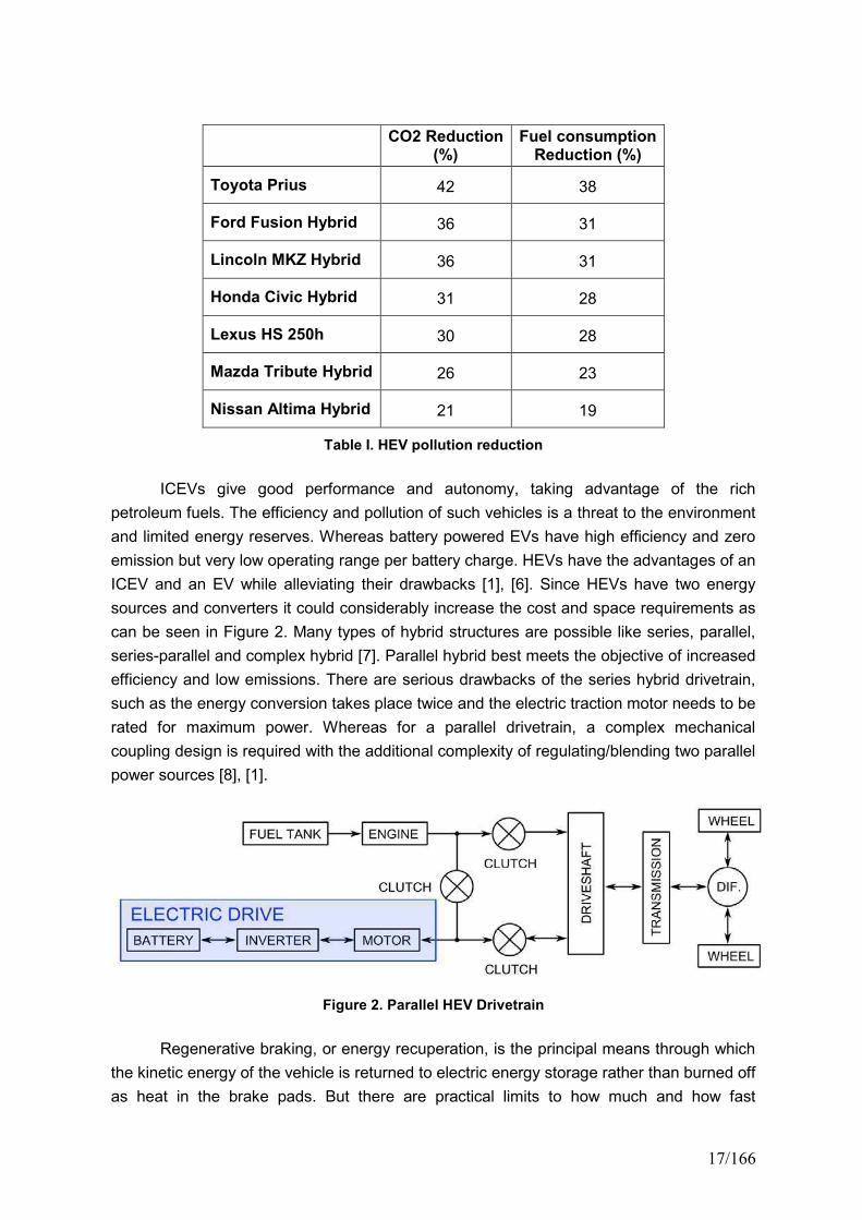
emissions can be reduced from 5% to 100%. Statistics for some HEVs are given in Table I.
Toyota Prius is most sold HEV.
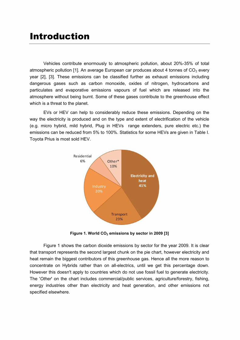
Figure 1. World CO2 emissions by sector in 2009 [3]
Figure 1 shows the carbon dioxide emissions by sector for the year 2009. It is clear
that transport represents the second largest chunk on the pie chart, however electricity and
heat remain the biggest contributors of this greenhouse gas. Hence all the more reason to
concentrate on Hybrids rather than on all-electrics, until we get this percentage down.
However this doesn't apply to countries which do not use fossil fuel to generate electricity.
The 'Other' on the chart includes commercial/public services, agriculture/forestry, fishing,
energy industries other than electricity and heat generation, and other emissions not
specified elsewhere.
17/166
CO2 Reduction(%)
Fuel consumptionReduction (%)
Toyota Prius 42 38
Ford Fusion Hybrid 36 31
Lincoln MKZ Hybrid 36 31
Honda Civic Hybrid 31 28
Lexus HS 250h 30 28
Mazda Tribute Hybrid 26 23
Nissan Altima Hybrid 21 19
Table I. HEV pollution reduction
ICEVs give good performance and autonomy, taking advantage of the rich
petroleum fuels. The efficiency and pollution of such vehicles is a threat to the environment
and limited energy reserves. Whereas battery powered EVs have high efficiency and zero
emission but very low operating range per battery charge. HEVs have the advantages of an
ICEV and an EV while alleviating their drawbacks [1], [6]. Since HEVs have two energy
sources and converters it could considerably increase the cost and space requirements as
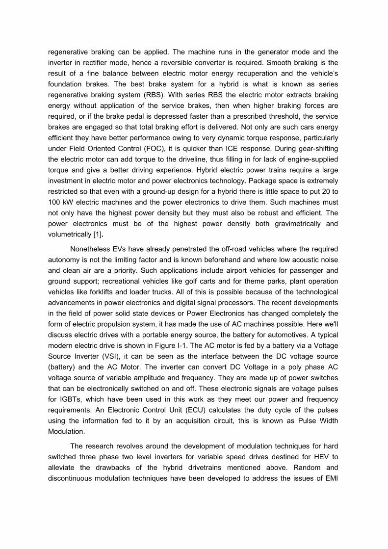
can be seen in Figure 2. Many types of hybrid structures are possible like series, parallel,
series-parallel and complex hybrid [7]. Parallel hybrid best meets the objective of increased
efficiency and low emissions. There are serious drawbacks of the series hybrid drivetrain,
such as the energy conversion takes place twice and the electric traction motor needs to be
rated for maximum power. Whereas for a parallel drivetrain, a complex mechanical
coupling design is required with the additional complexity of regulating/blending two parallel
power sources [8], [1].
Figure 2. Parallel HEV Drivetrain
Regenerative braking, or energy recuperation, is the principal means through which
the kinetic energy of the vehicle is returned to electric energy storage rather than burned off
as heat in the brake pads. But there are practical limits to how much and how fast
regenerative braking can be applied. The machine runs in the generator mode and the
inverter in rectifier mode, hence a reversible converter is required. Smooth braking is the
result of a fine balance between electric motor energy recuperation and the vehicle’s
foundation brakes. The best brake system for a hybrid is what is known as series
regenerative braking system (RBS). With series RBS the electric motor extracts braking
energy without application of the service brakes, then when higher braking forces are
required, or if the brake pedal is depressed faster than a prescribed threshold, the service
brakes are engaged so that total braking effort is delivered. Not only are such cars energy
efficient they have better performance owing to very dynamic torque response, particularly
under Field Oriented Control (FOC), it is quicker than ICE response. During gear-shifting
the electric motor can add torque to the driveline, thus filling in for lack of engine-supplied
torque and give a better driving experience. Hybrid electric power trains require a large
investment in electric motor and power electronics technology. Package space is extremely
restricted so that even with a ground-up design for a hybrid there is little space to put 20 to
100 kW electric machines and the power electronics to drive them. Such machines must
not only have the highest power density but they must also be robust and efficient. The
power electronics must be of the highest power density both gravimetrically and
volumetrically [1].
Nonetheless EVs have already penetrated the off-road vehicles where the required
autonomy is not the limiting factor and is known beforehand and where low acoustic noise
and clean air are a priority. Such applications include airport vehicles for passenger and
ground support; recreational vehicles like golf carts and for theme parks, plant operation
vehicles like forklifts and loader trucks. All of this is possible because of the technological
advancements in power electronics and digital signal processors. The recent developments
in the field of power solid state devices or Power Electronics has changed completely the
form of electric propulsion system, it has made the use of AC machines possible. Here we'll
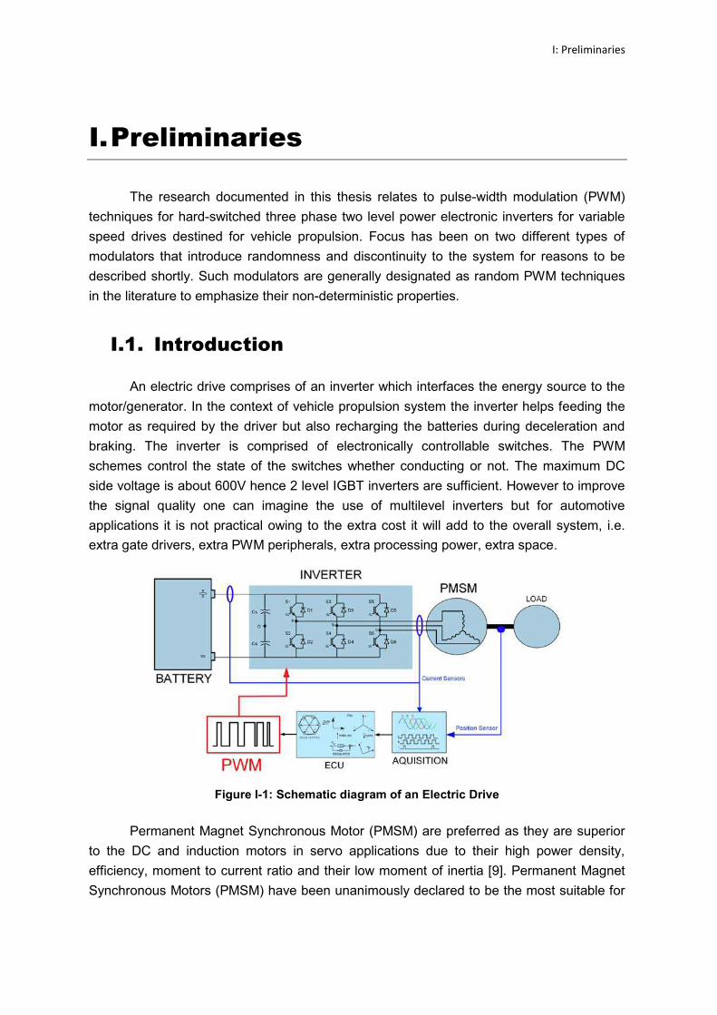
discuss electric drives with a portable energy source, the battery for automotives. A typical
modern electric drive is shown in Figure I-1. The AC motor is fed by a battery via a Voltage
Source Inverter (VSI), it can be seen as the interface between the DC voltage source
(battery) and the AC Motor. The inverter can convert DC Voltage in a poly phase AC
voltage source of variable amplitude and frequency. They are made up of power switches
that can be electronically switched on and off. These electronic signals are voltage pulses
for IGBTs, which have been used in this work as they meet our power and frequency
requirements. An Electronic Control Unit (ECU) calculates the duty cycle of the pulses
using the information fed to it by an acquisition circuit, this is known as Pulse Width
Modulation.
The research revolves around the development of modulation techniques for hard
switched three phase two level inverters for variable speed drives destined for HEV to
alleviate the drawbacks of the hybrid drivetrains mentioned above. Random and
discontinuous modulation techniques have been developed to address the issues of EMI
19/166
interference and switching losses respectively and their digital implementation has been
given equal importance. Techniques to reduce DC-link capacitors are also developed.
Hard switched PWM converters have the following drawbacks:
1) Electromagnetic pollution caused by the switching harmonics and switching
transients [11] may hamper the proper functioning of digital electronic circuitry used
extensively in modern cars. This is normally dealt by adding bulky and voluminous L-C
filters and shielding of the power converter.
2) Switching Losses [12] are not only a waste of energy but give rise to another very
important concern -- evacuating this energy dissipated in the form of heat in the power
switches. Thermal stress can lead to poor functioning and in extreme cases complete
failure of the switch.
3) Shaft voltages may cause an electric discharge through the lubricant around the
ball bearing and the stator called bearing current and destroy the motor [13].
4) Acoustic noise in power converters [14] for switching frequencies in the audible
range till 22kHz can be very annoying.
To alleviate these drawbacks this work has the objective of reducing the cost and
volume of the electric drivetrain by developing innovative PWM techniques to reduce the
need of auxiliary components required to suppress the side effects of such systems namely
EMI, DC link fluctuations and heating of the power switches and at the same time
increasing the efficiency and hence an improved autonomy on battery. These auxiliaries
are namely the passive filters to absorb the switching harmonics, DC stabilizing capacitors
and voluminous cooling circuit.
A very important aspect of this research is the integration of EMI mitigation
techniques and meeting Electromagnetic Compatibility (EMC) standards at the
development stages of the electric drive rather than troubleshooting at the end, which is a
costly and time-consuming process. The motivation behind the work is to reduce the cost to
market of HEVs which is significantly higher than conventional cars. Innovative techniques
based on the classical PWM techniques such as RPWM and DPWM exist to address the
issue of unwanted harmonics linked to the switching frequency and the switching losses.
These techniques are explained in the chapters to follow. Space Vector Modulation (SVM)
is a relatively new PWM technique based on mathematical transformations and has some
advantages over conventional techniques. Since more and more sophisticated techniques
are used, such as FOC, DTC, the digital signal processors have become indispensible and
this means SVM can be implemented at no extra cost. SVM has been taken as the basic
modulation technique and its derivatives are developed to address the issues mentioned
above.
In such electric drives, PWM methods influence heavily the behaviour of the drive. A
meticulously programmed technique cannot only give improved performance but also
reduce many of the unwanted secondary effects of modulated power supply. The work

presented here is on developing such PWM techniques to alleviate the problems in the
drives mentioned in the previous section.
The thesis is divided into four parts, the first part puts into perspective the need for
this study and an assessment of the state of the art of the field, explaining briefly the major
problems that need to be addressed. Introduction to EMI is given and then an overview of
some performance indicators of Pulse Width Modulators. The second part gives details of
the PWM techniques developed during this PhD. The third part gives the details of the
experimental setup and the experimental validations of the techniques developed in the
second part. The fourth part is the conclusion and few suggestions for future works.

21/166
PART I
PRELIMINARIES
I: Preliminaries
I.Preliminaries
The research documented in this thesis relates to pulse-width modulation (PWM)
techniques for hard-switched three phase two level power electronic inverters for variable
speed drives destined for vehicle propulsion. Focus has been on two different types of
modulators that introduce randomness and discontinuity to the system for reasons to be
described shortly. Such modulators are generally designated as random PWM techniques
in the literature to emphasize their non-deterministic properties.
I.1. Introduction
An electric drive comprises of an inverter which interfaces the energy source to the
motor/generator. In the context of vehicle propulsion system the inverter helps feeding the
motor as required by the driver but also recharging the batteries during deceleration and
braking. The inverter is comprised of electronically controllable switches. The PWM
schemes control the state of the switches whether conducting or not. The maximum DC
side voltage is about 600V hence 2 level IGBT inverters are sufficient. However to improve
the signal quality one can imagine the use of multilevel inverters but for automotive
applications it is not practical owing to the extra cost it will add to the overall system, i.e.
extra gate drivers, extra PWM peripherals, extra processing power, extra space.
Figure I-1: Schematic diagram of an Electric Drive
Permanent Magnet Synchronous Motor (PMSM) are preferred as they are superior
to the DC and induction motors in servo applications due to their high power density,
efficiency, moment to current ratio and their low moment of inertia [9]. Permanent Magnet
Synchronous Motors (PMSM) have been unanimously declared to be the most suitable for
23/166
HEVs. Table I-1 recapitulates how different electrical machines fair on grounds mentioned
above.
DC IM PMSM SRM
Power Density -- + ++ 0
Efficiency -- + ++ 0
Cost + + 0 +
Table I-1 Comparison of Electrical Machines
The two most pertinent control schemes for AC motors are Field Oriented Control
(FOC) and Direct Torque Control (DTC). The former was chosen because DTC is a method
based on hysteresis comparators which require the controller to work at a very high
frequency in order to confine the error in the hysteresis band which means introducing error
to the system and hence torque ripple. FOC unlike DTC is based on regulators which
calculate the exact value of the phase voltage to be fed to the motor. PWM techniques are
used to calculate the duty cycle of the pulse to be applied to the switch to produce the
required output voltage to be applied to the motor [10]. PWM techniques are at the heart of
such drives, they have a huge influence on various aspects apart from the quality of the
voltage produced, like the losses and electromagnetic interference.
I.2. Literature review
Pulse Width Modulation is an interface between the control circuit and the inverter,
where the modulator is given a value that is required at the converter terminal and it has to
produce it for a given period and a given DC voltage. Modulation technique was developed
by communication engineers to transmit a baseband signal by transforming it into a pass-
band signal. The use of PWM for electric drives dates as back as the early 1960s [15].
The concept is to achieve a variable voltage from a fixed DC voltage source while
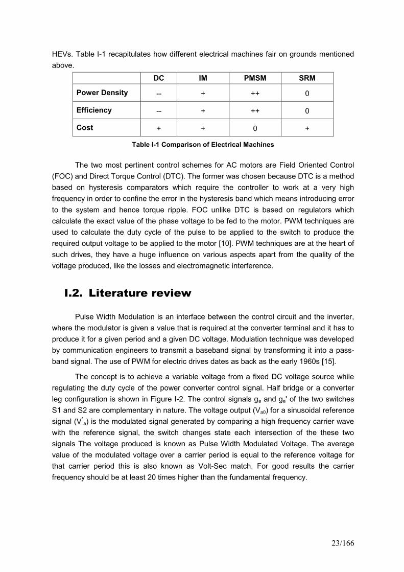
regulating the duty cycle of the power converter control signal. Half bridge or a converter
leg configuration is shown in Figure I-2. The control signals ga and ga' of the two switches
S1 and S2 are complementary in nature. The voltage output (Va0) for a sinusoidal reference
signal (V*a) is the modulated signal generated by comparing a high frequency carrier wave
with the reference signal, the switch changes state each intersection of the these two
signals The voltage produced is known as Pulse Width Modulated Voltage. The average
value of the modulated voltage over a carrier period is equal to the reference voltage for
that carrier period this is also known as Volt-Sec match. For good results the carrier
frequency should be at least 20 times higher than the fundamental frequency.
I: Preliminaries
Figure I-2: Half Bridge
I.2.1. Fundamentals of PWM
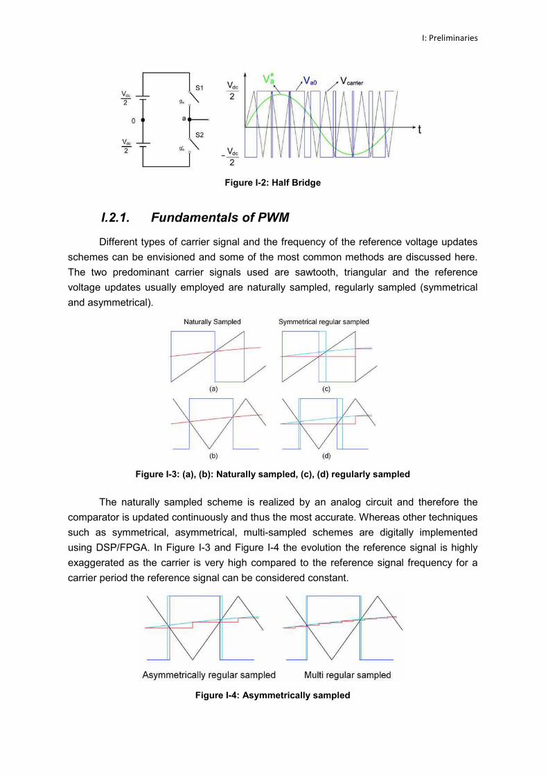
Different types of carrier signal and the frequency of the reference voltage updates
schemes can be envisioned and some of the most common methods are discussed here.
The two predominant carrier signals used are sawtooth, triangular and the reference
voltage updates usually employed are naturally sampled, regularly sampled (symmetrical
and asymmetrical).
Figure I-3: (a), (b): Naturally sampled, (c), (d) regularly sampled
The naturally sampled scheme is realized by an analog circuit and therefore the
comparator is updated continuously and thus the most accurate. Whereas other techniques
such as symmetrical, asymmetrical, multi-sampled schemes are digitally implemented
using DSP/FPGA. In Figure I-3 and Figure I-4 the evolution the reference signal is highly
exaggerated as the carrier is very high compared to the reference signal frequency for a
carrier period the reference signal can be considered constant.
Figure I-4: Asymmetrically sampled
25/166
I.2.2. Classical Sinusoidal PWM
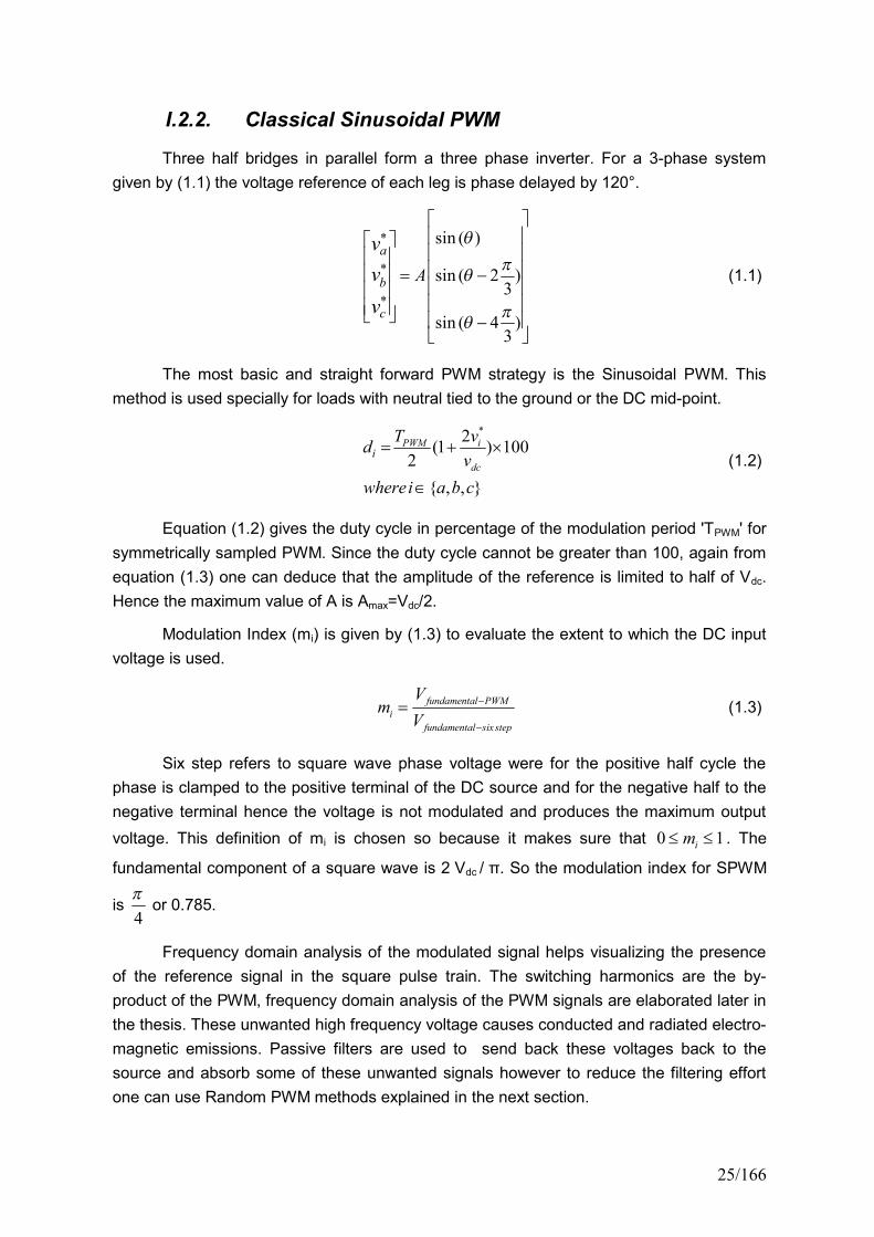
Three half bridges in parallel form a three phase inverter. For a 3-phase system
given by (1.1) the voltage reference of each leg is phase delayed by 120°.
*
*
*
sin ( )
sin ( 2 )3
sin ( 4 )3
a
b
c
A
v
v
v
(1.1)
The most basic and straight forward PWM strategy is the Sinusoidal PWM. This
method is used specially for loads with neutral tied to the ground or the DC mid-point.
*2(1 ) 100
2
{ , , }
PWM i
dc
i
T vd
v
wherei a b c
(1.2)
Equation (1.2) gives the duty cycle in percentage of the modulation period 'TPWM' for
symmetrically sampled PWM. Since the duty cycle cannot be greater than 100, again from
equation (1.3) one can deduce that the amplitude of the reference is limited to half of Vdc.
Hence the maximum value of A is Amax=Vdc/2.
Modulation Index (mi) is given by (1.3) to evaluate the extent to which the DC input
voltage is used.
fundamental PWM
i
fundamental six step
Vm
V
(1.3)
Six step refers to square wave phase voltage were for the positive half cycle the
phase is clamped to the positive terminal of the DC source and for the negative half to the
negative terminal hence the voltage is not modulated and produces the maximum output
voltage. This definition of mi is chosen so because it makes sure that 0 1im . The
fundamental component of a square wave is 2 Vdc / π. So the modulation index for SPWM
is4
or 0.785.
Frequency domain analysis of the modulated signal helps visualizing the presence
of the reference signal in the square pulse train. The switching harmonics are the by-
product of the PWM, frequency domain analysis of the PWM signals are elaborated later in
the thesis. These unwanted high frequency voltage causes conducted and radiated electro-
magnetic emissions. Passive filters are used to send back these voltages back to the
source and absorb some of these unwanted signals however to reduce the filtering effort
one can use Random PWMmethods explained in the next section.
I: Preliminaries
I.2.3. Hysteresis Band control
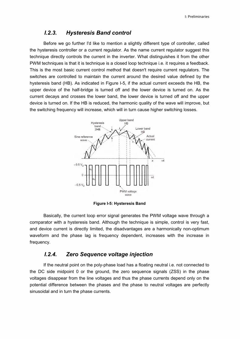
Before we go further I'd like to mention a slightly different type of controller, called
the hysteresis controller or a current regulator. As the name current regulator suggest this
technique directly controls the current in the inverter. What distinguishes it from the other
PWM techniques is that it is technique is a closed loop technique i.e. it requires a feedback.
This is the most basic current control method that doesn't require current regulators. The
switches are controlled to maintain the current around the desired value defined by the
hysteresis band (HB). As indicated in Figure I-5, if the actual current exceeds the HB, the
upper device of the half-bridge is turned off and the lower device is turned on. As the
current decays and crosses the lower band, the lower device is turned off and the upper
device is turned on. If the HB is reduced, the harmonic quality of the wave will improve, but
the switching frequency will increase, which will in turn cause higher switching losses.
Figure I-5: Hysteresis Band
Basically, the current loop error signal generates the PWM voltage wave through a
comparator with a hysteresis band. Although the technique is simple, control is very fast,
and device current is directly limited, the disadvantages are a harmonically non-optimum
waveform and the phase lag is frequency dependent, increases with the increase in
frequency.
I.2.4. Zero Sequence voltage injection
If the neutral point on the poly-phase load has a floating neutral i.e. not connected to
the DC side midpoint 0 or the ground, the zero sequence signals (ZSS) in the phase
voltages disappear from the line voltages and thus the phase currents depend only on the
potential difference between the phases and the phase to neutral voltages are perfectly
sinusoidal and in turn the phase currents.
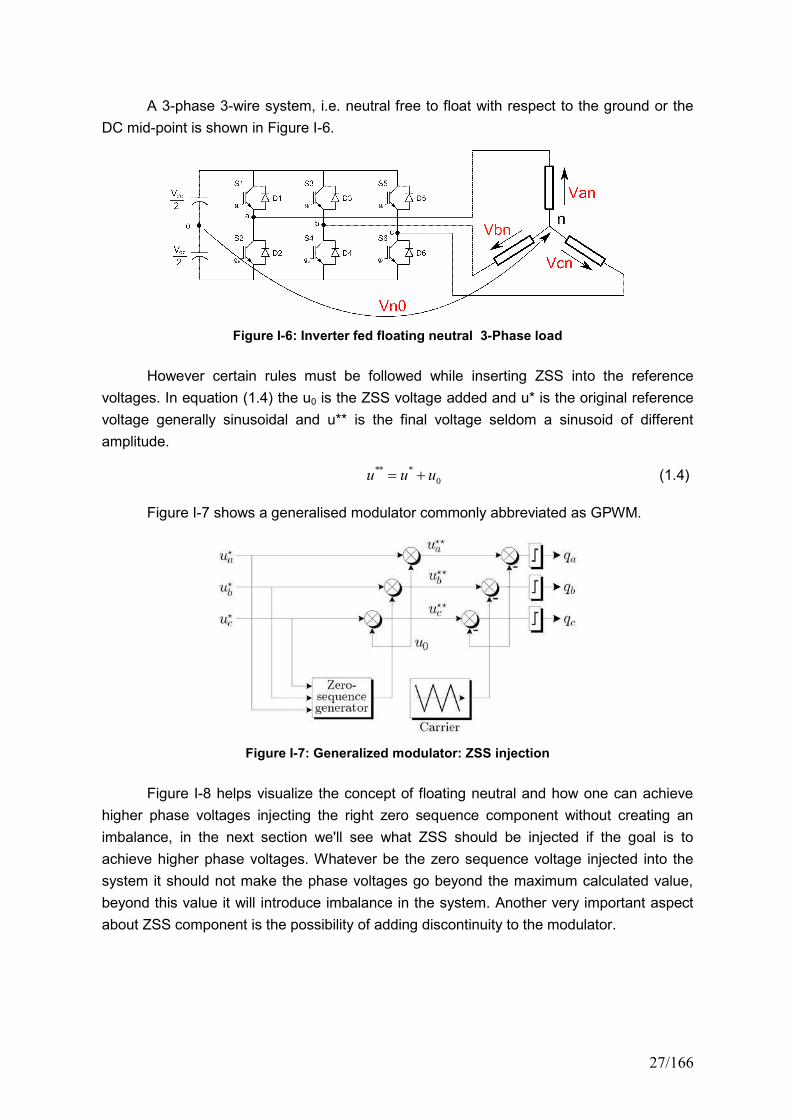
27/166
A 3-phase 3-wire system, i.e. neutral free to float with respect to the ground or the
DC mid-point is shown in Figure I-6.
Figure I-6: Inverter fed floating neutral 3-Phase load
However certain rules must be followed while inserting ZSS into the reference
voltages. In equation (1.4) the u0 is the ZSS voltage added and u* is the original reference
voltage generally sinusoidal and u** is the final voltage seldom a sinusoid of different
amplitude.
** *0u u u (1.4)
Figure I-7 shows a generalised modulator commonly abbreviated as GPWM.
Figure I-7: Generalized modulator: ZSS injection
Figure I-8 helps visualize the concept of floating neutral and how one can achieve
higher phase voltages injecting the right zero sequence component without creating an
imbalance, in the next section we'll see what ZSS should be injected if the goal is to
achieve higher phase voltages. Whatever be the zero sequence voltage injected into the
system it should not make the phase voltages go beyond the maximum calculated value,
beyond this value it will introduce imbalance in the system. Another very important aspect
about ZSS component is the possibility of adding discontinuity to the modulator.
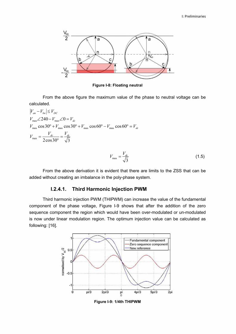
I: Preliminaries
Figure I-8: Floating neutral
From the above figure the maximum value of the phase to neutral voltage can be
calculated.
max max
max max max max
max
240 0
cos30 cos30 cos60 cos60
2cos30 3
an bn DC
dc
dc
dc dc
V V V
V V V
V V V V V
V VV
max3dcVV (1.5)
From the above derivation it is evident that there are limits to the ZSS that can be
added without creating an imbalance in the poly-phase system.
I.2.4.1. Third Harmonic Injection PWM
Third harmonic injection PWM (THIPWM) can increase the value of the fundamental
component of the phase voltage, Figure I-9 shows that after the addition of the zero
sequence component the region which would have been over-modulated or un-modulated
is now under linear modulation region. The optimum injection value can be calculated as
following: [16].
Figure I-9: 1/4th THIPWM

29/166
The most prominent third harmonic injection schemes are THIPWM1/4 and
THIPWM1/6 where the zero sequence voltage to be injected is given by (1.6).
0 3
1 13 3
cos(3 )
4 6
u A t
A AA or A
(1.6)
Where A1 and A3 are the amplitudes of the fundamental and the third harmonic
components respectively. Injecting ¼ of the fundamental is theoretically superior in terms of
harmonic distortion [17] while injecting 1/6 increases the fundamental to the maximum
possible value , this can be shown in the following manner: Let Eq.(1.7) give the resultant
voltage after third-harmonic injection.
1 3cos cos32dc
a
VV M M (1.7)
Dividing by 12
dcM Vwe get:
cos cos3v Where 3
1
MM
.
sin 3 sin3 0dv
dt (1.8)
The maxima or minima of (1.7) would lie on the values of θ and that satisfy
equation (1.8) and sin3θ can be written as:
2sin3 (4cos 1)sin Substituting it in equation (1.8) gives
2sin 3 (4cos 1)sin 0 from where the value of cosθ can be calculated as:
3 1cos
12
(1.9)
cos3θ can similarly be expanded to give as 2cos3 (4cos 3) cos and therefore
6 1 3 1cos3
6 12
.
Substituting these values back in (1.8) give:
max
3 1 3 1
3 3v
(1.10)
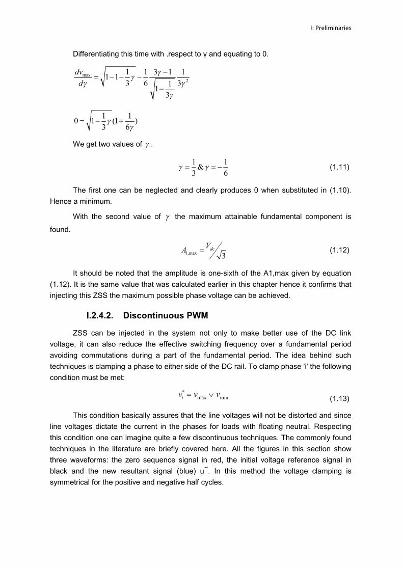
I: Preliminaries
Differentiating this time with .respect to γ and equating to 0.
max2
1 1 3 1 11 1
3 6 3113
dv
d
1 10 1 (1 )
3 6
We get two values of .1 1&3 6
(1.11)
The first one can be neglected and clearly produces 0 when substituted in (1.10).
Hence a minimum.
With the second value of the maximum attainable fundamental component is
found.
1,max 3dcVA (1.12)
It should be noted that the amplitude is one-sixth of the A1,max given by equation
(1.12). It is the same value that was calculated earlier in this chapter hence it confirms that
injecting this ZSS the maximum possible phase voltage can be achieved.
I.2.4.2. Discontinuous PWM
ZSS can be injected in the system not only to make better use of the DC link
voltage, it can also reduce the effective switching frequency over a fundamental period
avoiding commutations during a part of the fundamental period. The idea behind such
techniques is clamping a phase to either side of the DC rail. To clamp phase 'i' the following
condition must be met:
*max miniv v v (1.13)
This condition basically assures that the line voltages will not be distorted and since
line voltages dictate the current in the phases for loads with floating neutral. Respecting
this condition one can imagine quite a few discontinuous techniques. The commonly found
techniques in the literature are briefly covered here. All the figures in this section show
three waveforms: the zero sequence signal in red, the initial voltage reference signal in
black and the new resultant signal (blue) u**. In this method the voltage clamping is
symmetrical for the positive and negative half cycles.
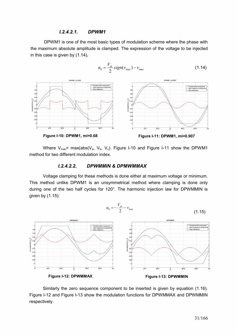
31/166
I.2.4.2.1. DPWM1
DPWM1 is one of the most basic types of modulation scheme where the phase with
the maximum absolute amplitude is clamped. The expression of the voltage to be injected
in this case is given by (1.14).
0 max max( )2dcVu sign v v (1.14)
Figure I-10: DPWM1, mi=0.68 Figure I-11: DPWM1, mi=0.907
Where Vmax= max(abs(Va, Vb, Vc). Figure I-10 and Figure I-11 show the DPWM1
method for two different modulation index.
I.2.4.2.2. DPWMMIN & DPMWMMAX
Voltage clamping for these methods is done either at maximum voltage or minimum.
This method unlike DPWM1 is an unsymmetrical method where clamping is done only
during one of the two half cycles for 120°. The harmonic injection law for DPWMMIN is
given by (1.15):
0 min2dcVu v
(1.15)
Figure I-12: DPWMMAX Figure I-13: DPWMMIN
Similarly the zero sequence component to be inserted is given by equation (1.16).
Figure I-12 and Figure I-13 show the modulation functions for DPWMMAX and DPWMMIN
respectively.
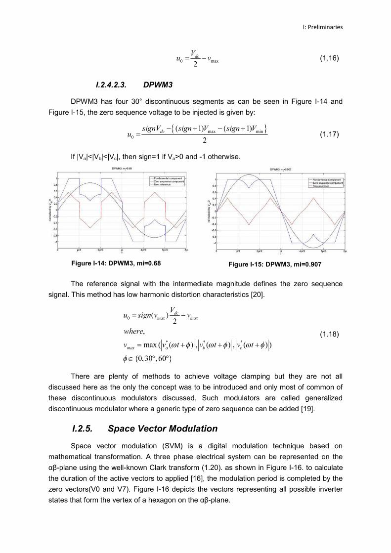
I: Preliminaries
0 max2dcVu v (1.16)
I.2.4.2.3. DPWM3
DPWM3 has four 30° discontinuous segments as can be seen in Figure I-14 and
Figure I-15, the zero sequence voltage to be injected is given by:
max min0
( 1) ( 1)
2dcsignV sign V sign V
u (1.17)
If |Va|<|Vb|<|Vc|, then sign=1 if Va>0 and -1 otherwise.
Figure I-14: DPWM3, mi=0.68 Figure I-15: DPWM3, mi=0.907
The reference signal with the intermediate magnitude defines the zero sequence
signal. This method has low harmonic distortion characteristics [20].
0
* * *
( )2
,
max ( ( ) , ( ) , ( ) )
{0,30 ,60 }
dcmax max
max a b c
Vu sign v v
where
v v t v t v t
(1.18)
There are plenty of methods to achieve voltage clamping but they are not all
discussed here as the only the concept was to be introduced and only most of common of
these discontinuous modulators discussed. Such modulators are called generalized
discontinuous modulator where a generic type of zero sequence can be added [19].
I.2.5. Space Vector Modulation
Space vector modulation (SVM) is a digital modulation technique based on
mathematical transformation. A three phase electrical system can be represented on the
αβ-plane using the well-known Clark transform (1.20). as shown in Figure I-16. to calculate the duration of the active vectors to applied [16], the modulation period is completed by the
zero vectors(V0 and V7). Figure I-16 depicts the vectors representing all possible inverter
states that form the vertex of a hexagon on the αβ-plane.
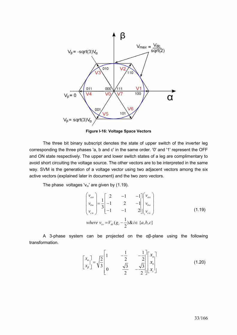
33/166
Figure I-16: Voltage Space Vectors
The three bit binary subscript denotes the state of upper switch of the inverter leg
corresponding the three phases 'a, b and c' in the same order. '0' and '1' represent the OFF
and ON state respectively. The upper and lower switch states of a leg are complimentary to
avoid short circuiting the voltage source. The other vectors are to be interpreted in the same
way. SVM is the generation of a voltage vector using two adjacent vectors among the six
active vectors (explained later in document) and the two zero vectors.
The phase voltages 'vin' are given by (1.19).
2 1 11
1 2 13
1 1 2
1( )& { , , }
2
an ao
bn bo
cn co
io dc i
v v
v v
v v
where v V g i a b c
(1.19)
A 3-phase system can be projected on the αβ-plane using the following transformation.
1 11
2 2 2
3 3 30
2 2
a
b
c
x
x
x
x
x
(1.20)

I: Preliminaries
Applying (1.20) and (1.19) on (1.1) we get the projections in the αβ-plane as shown in the Table I-2.
ga gb gc vα vβ Vector
0 0 0 0 0 V0
0 0 16dcV
2dcV V5
0 1 06dcV
2dcV V3
0 1 1 2
6dcV 0 V4
1 0 0 2
6dcV 0 V1
1 0 16dcV
2dcV V6
1 1 06dcV
2dcV V2
1 1 1 0 0 V7
Table I-2 Vector magnitudes in αβ-plane
The magnitudes of all the active vectors can be given by (1.21).
2
3{1,2,3,4,5,6}
i dcV V
wherei
(1.21)
Using (1.20) a balanced three phase system expressed by (1.1) can be represented
by a circle whose radius is given by A.
3sin( ),
2
3cos( )
2
v A
v A
(1.22)
2 2 3
2v v A (1.23)
Let Amax be the maximum amplitude of the 3-phase Voltage that can be generated
using the space vectors shown in Figure I-16. Then the radius of such system is given by
(1.24).
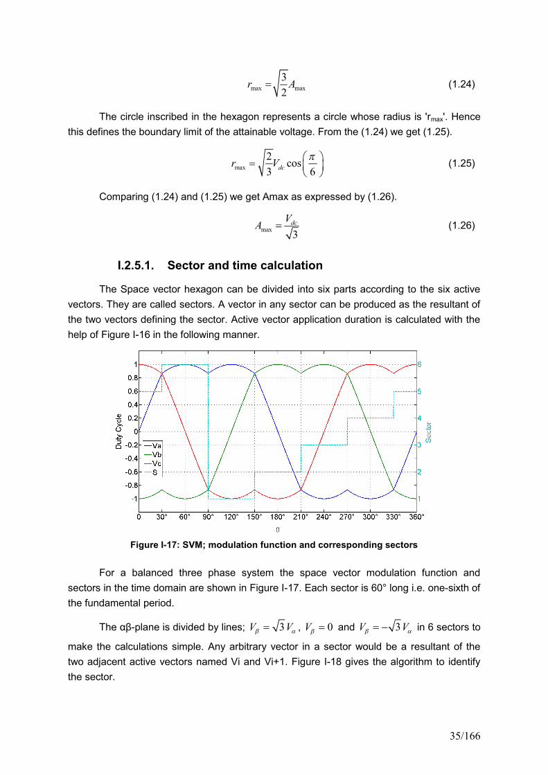
35/166
max max
3
2r A (1.24)
The circle inscribed in the hexagon represents a circle whose radius is 'rmax'. Hence
this defines the boundary limit of the attainable voltage. From the (1.24) we get (1.25).
max
2cos
3 6dcr V (1.25)
Comparing (1.24) and (1.25) we get Amax as expressed by (1.26).
max3dcVA (1.26)
I.2.5.1. Sector and time calculation
The Space vector hexagon can be divided into six parts according to the six active
vectors. They are called sectors. A vector in any sector can be produced as the resultant of
the two vectors defining the sector. Active vector application duration is calculated with the
help of Figure I-16 in the following manner.
Figure I-17: SVM; modulation function and corresponding sectors
For a balanced three phase system the space vector modulation function and
sectors in the time domain are shown in Figure I-17. Each sector is 60° long i.e. one-sixth of
the fundamental period.
The αβ-plane is divided by lines; 3V V , 0V and 3V V in 6 sectors to
make the calculations simple. Any arbitrary vector in a sector would be a resultant of the
two adjacent active vectors named Vi and Vi+1. Figure I-18 gives the algorithm to identify
the sector.
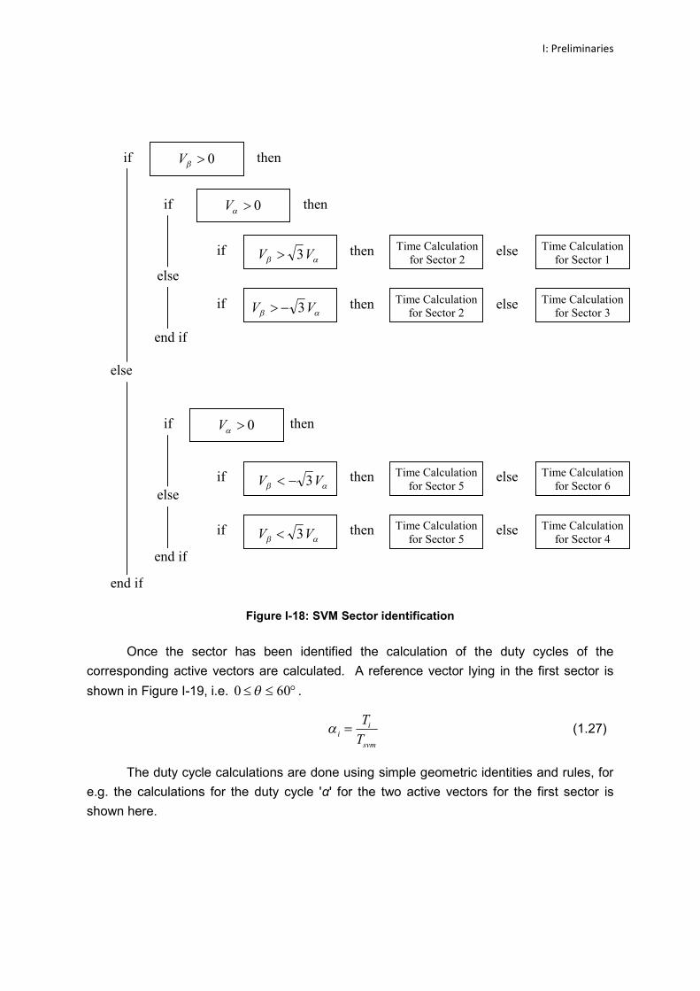
I: Preliminaries
Figure I-18: SVM Sector identification
Once the sector has been identified the calculation of the duty cycles of the
corresponding active vectors are calculated. A reference vector lying in the first sector is
shown in Figure I-19, i.e. 0 60 .i
i
svm
T
T (1.27)
The duty cycle calculations are done using simple geometric identities and rules, for
e.g. the calculations for the duty cycle 'α' for the two active vectors for the first sector isshown here.
Time Calculationfor Sector 2
Time Calculationfor Sector 1
Time Calculationfor Sector 2
Time Calculationfor Sector 3
Time Calculationfor Sector 5
Time Calculationfor Sector 6
Time Calculationfor Sector 5
Time Calculationfor Sector 4
then
then
then
then
then
then
then
else
else
else
else
if
if
if
if
if
else
end if
if
else
end if
if
else
end if
0V
VV 3
0V
VV 3
VV 3
VV 3
0V
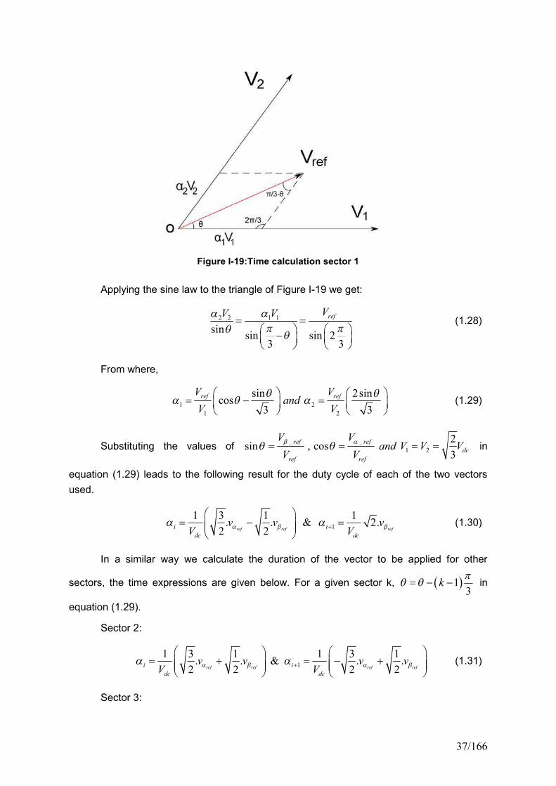
37/166
Figure I-19:Time calculation sector 1
Applying the sine law to the triangle of Figure I-19 we get:
2 2 1 1
sinsin sin 2
3 3
refVV V
(1.28)
From where,
1 21 2
sin 2sincos
3 3ref refV V
andV V
(1.29)
Substituting the values of_ _
1 2
2sin , cos
3ref ref
dc
ref ref
V Vand V V V
V V
in
equation (1.29) leads to the following result for the duty cycle of each of the two vectors
used.
1
1 3 1 1. . & 2.2 2ref ref refi i
dc dc
v v vV V
(1.30)
In a similar way we calculate the duration of the vector to be applied for other
sectors, the time expressions are given below. For a given sector k, 13
k in
equation (1.29).
Sector 2:
1
1 3 1 1 3 1. . & . .2 2 2 2ref ref ref refi i
dc dc
v v v vV V
(1.31)
Sector 3:
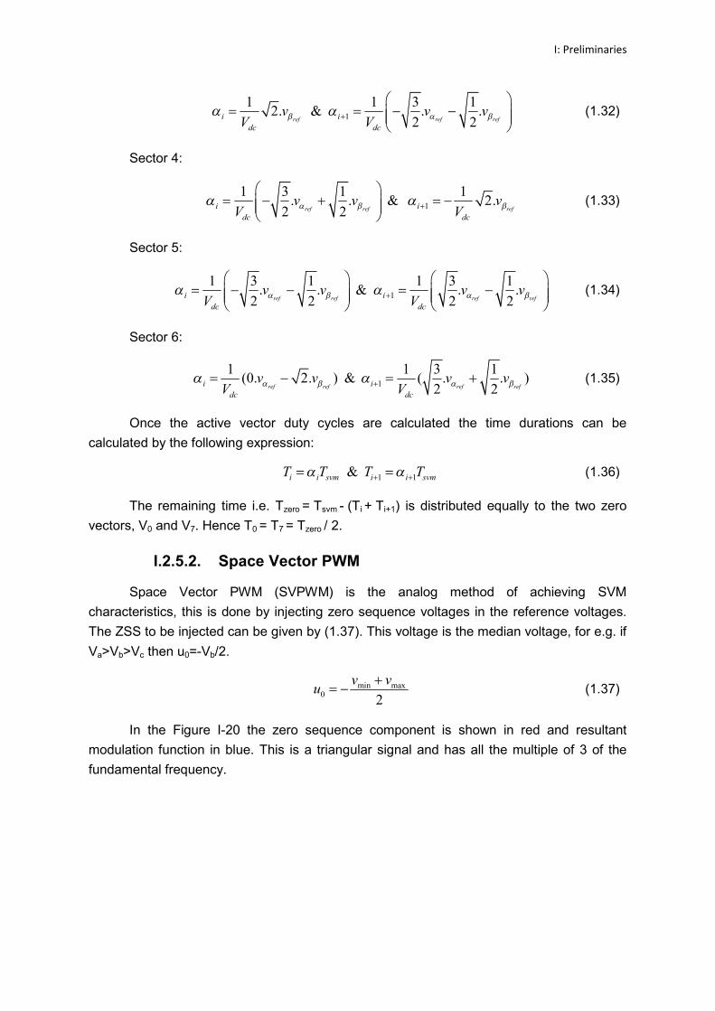
I: Preliminaries
1
1 1 3 12. & . .
2 2ref ref refi i
dc dc
v v vV V
(1.32)
Sector 4:
1
1 3 1 1. . & 2.2 2ref ref refi i
dc dc
v v vV V
(1.33)
Sector 5:
1
1 3 1 1 3 1. . & . .2 2 2 2ref ref ref refi i
dc dc
v v v vV V
(1.34)
Sector 6:
1
1 1 3 1(0. 2. ) & ( . . )
2 2ref ref ref refi i
dc dc
v v v vV V
(1.35)
Once the active vector duty cycles are calculated the time durations can be
calculated by the following expression:
1 1&i i svm i i svmT T T T (1.36)
The remaining time i.e. Tzero = Tsvm - (Ti + Ti+1) is distributed equally to the two zero
vectors, V0 and V7. Hence T0= T7= Tzero / 2.
I.2.5.2. Space Vector PWM
Space Vector PWM (SVPWM) is the analog method of achieving SVM
characteristics, this is done by injecting zero sequence voltages in the reference voltages.
The ZSS to be injected can be given by (1.37). This voltage is the median voltage, for e.g. if
Va>Vb>Vc then u0=-Vb/2.
min max0 2
v vu
(1.37)
In the Figure I-20 the zero sequence component is shown in red and resultant
modulation function in blue. This is a triangular signal and has all the multiple of 3 of the
fundamental frequency.
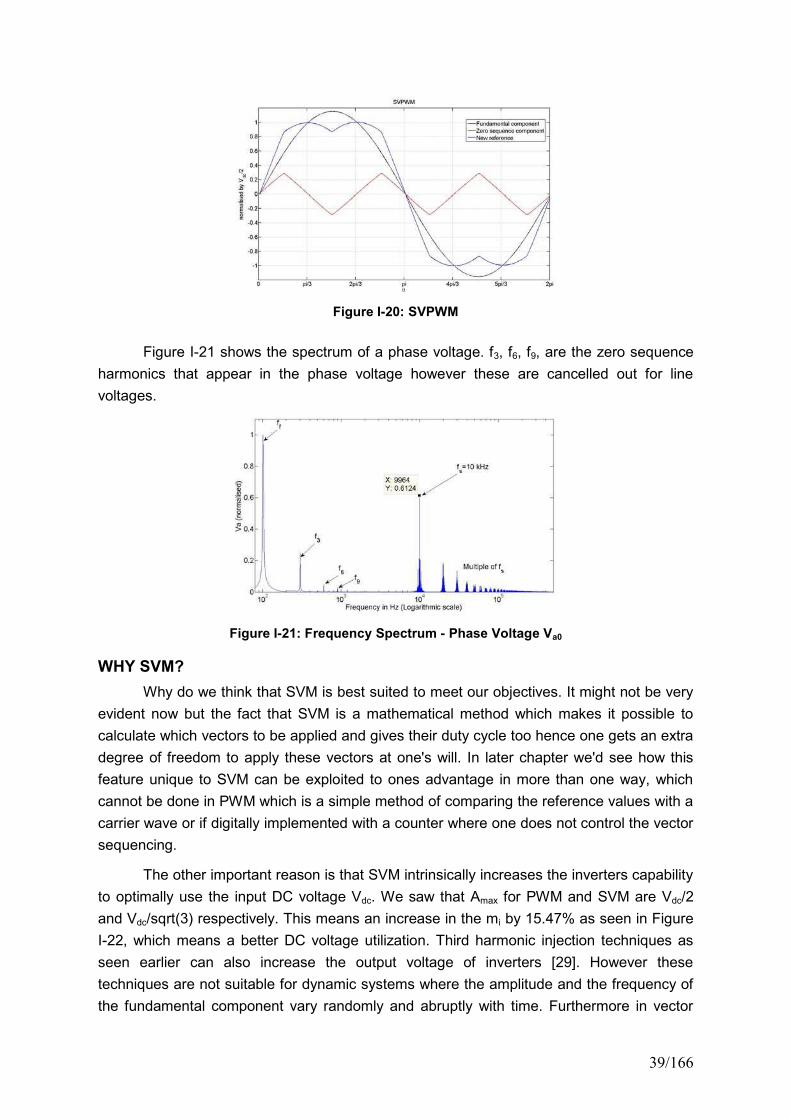
39/166
Figure I-20: SVPWM
Figure I-21 shows the spectrum of a phase voltage. f3, f6, f9, are the zero sequence
harmonics that appear in the phase voltage however these are cancelled out for line
voltages.
Figure I-21: Frequency Spectrum - Phase Voltage Va0
WHY SVM?
Why do we think that SVM is best suited to meet our objectives. It might not be very
evident now but the fact that SVM is a mathematical method which makes it possible to
calculate which vectors to be applied and gives their duty cycle too hence one gets an extra
degree of freedom to apply these vectors at one's will. In later chapter we'd see how this
feature unique to SVM can be exploited to ones advantage in more than one way, which
cannot be done in PWM which is a simple method of comparing the reference values with a
carrier wave or if digitally implemented with a counter where one does not control the vector
sequencing.
The other important reason is that SVM intrinsically increases the inverters capability
to optimally use the input DC voltage Vdc. We saw that Amax for PWM and SVM are Vdc/2
and Vdc/sqrt(3) respectively. This means an increase in the mi by 15.47% as seen in Figure
I-22, which means a better DC voltage utilization. Third harmonic injection techniques as
seen earlier can also increase the output voltage of inverters [29]. However these
techniques are not suitable for dynamic systems where the amplitude and the frequency of
the fundamental component vary randomly and abruptly with time. Furthermore in vector
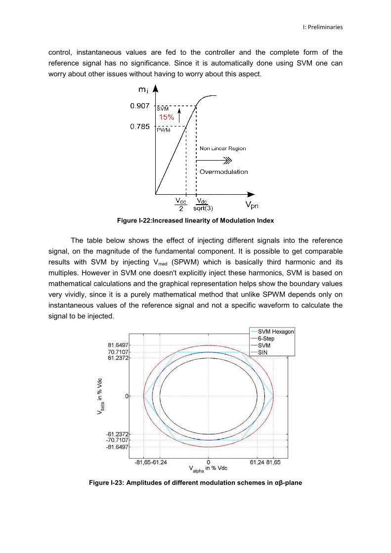
I: Preliminaries
control, instantaneous values are fed to the controller and the complete form of the
reference signal has no significance. Since it is automatically done using SVM one can
worry about other issues without having to worry about this aspect.
Figure I-22:Increased linearity of Modulation Index
The table below shows the effect of injecting different signals into the reference
signal, on the magnitude of the fundamental component. It is possible to get comparable
results with SVM by injecting Vmed (SPWM) which is basically third harmonic and its
multiples. However in SVM one doesn't explicitly inject these harmonics, SVM is based on
mathematical calculations and the graphical representation helps show the boundary values
very vividly, since it is a purely mathematical method that unlike SPWM depends only on
instantaneous values of the reference signal and not a specific waveform to calculate the
signal to be injected.
Figure I-23: Amplitudes of different modulation schemes in αβ-plane
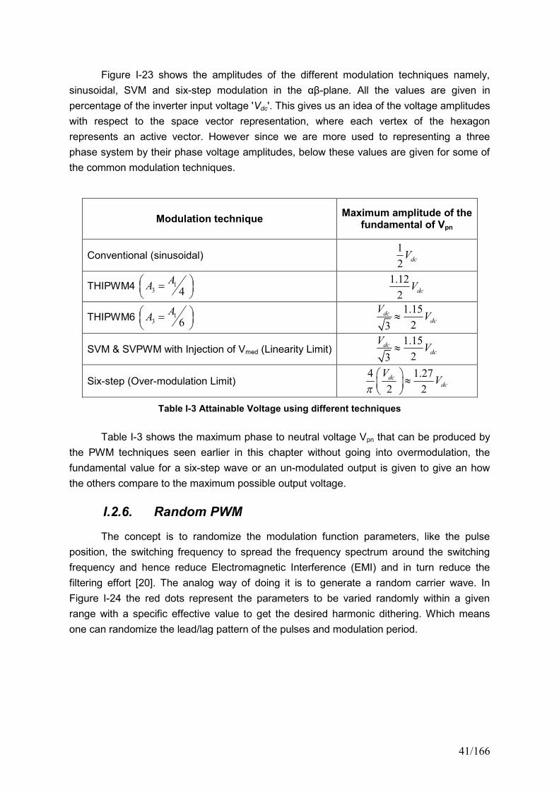
41/166
Figure I-23 shows the amplitudes of the different modulation techniques namely,
sinusoidal, SVM and six-step modulation in the αβ-plane. All the values are given in percentage of the inverter input voltage 'Vdc'. This gives us an idea of the voltage amplitudes
with respect to the space vector representation, where each vertex of the hexagon
represents an active vector. However since we are more used to representing a three
phase system by their phase voltage amplitudes, below these values are given for some of
the common modulation techniques.
Modulation techniqueMaximum amplitude of the
fundamental of Vpn
Conventional (sinusoidal)1
2 dcV
THIPWM4 13 4A
A 1.12
2 dcV
THIPWM6 13 6A
A 1.15
23dc
dc
VV
SVM & SVPWM with Injection of Vmed (Linearity Limit)1.15
23dc
dc
VV
Six-step (Over-modulation Limit)4 1.27
2 2dc
dc
VV
Table I-3 Attainable Voltage using different techniques
Table I-3 shows the maximum phase to neutral voltage Vpn that can be produced by
the PWM techniques seen earlier in this chapter without going into overmodulation, the
fundamental value for a six-step wave or an un-modulated output is given to give an how
the others compare to the maximum possible output voltage.
I.2.6. Random PWM
The concept is to randomize the modulation function parameters, like the pulse
position, the switching frequency to spread the frequency spectrum around the switching
frequency and hence reduce Electromagnetic Interference (EMI) and in turn reduce the
filtering effort [20]. The analog way of doing it is to generate a random carrier wave. In
Figure I-24 the red dots represent the parameters to be varied randomly within a given
range with a specific effective value to get the desired harmonic dithering. Which means
one can randomize the lead/lag pattern of the pulses and modulation period.
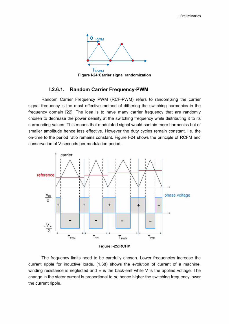
I: Preliminaries
Figure I-24:Carrier signal randomization
I.2.6.1. Random Carrier Frequency-PWM
Random Carrier Frequency PWM (RCF-PWM) refers to randomizing the carrier
signal frequency is the most effective method of dithering the switching harmonics in the
frequency domain [22]. The idea is to have many carrier frequency that are randomly
chosen to decrease the power density at the switching frequency while distributing it to its
surrounding values. This means that modulated signal would contain more harmonics but of
smaller amplitude hence less effective. However the duty cycles remain constant, i.e. the
on-time to the period ratio remains constant. Figure I-24 shows the principle of RCFM and
conservation of V-seconds per modulation period.
Figure I-25:RCFM
The frequency limits need to be carefully chosen. Lower frequencies increase the
current ripple for inductive loads. (1.38) shows the evolution of current of a machine,
winding resistance is neglected and E is the back-emf while V is the applied voltage. The
change in the stator current is proportional to dt, hence higher the switching frequency lower
the current ripple.
TPWM
δ PWM
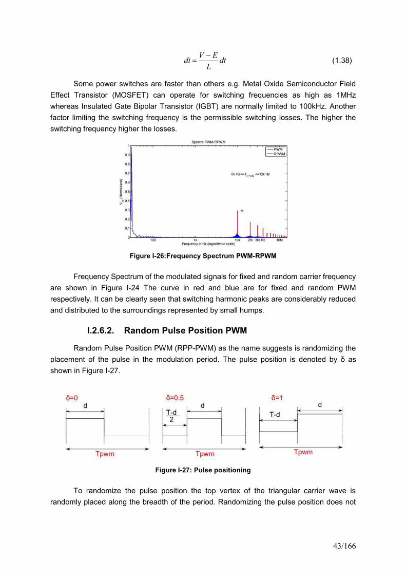
43/166
V Edi dt
L
(1.38)
Some power switches are faster than others e.g. Metal Oxide Semiconductor Field
Effect Transistor (MOSFET) can operate for switching frequencies as high as 1MHz
whereas Insulated Gate Bipolar Transistor (IGBT) are normally limited to 100kHz. Another
factor limiting the switching frequency is the permissible switching losses. The higher the
switching frequency higher the losses.
Figure I-26:Frequency Spectrum PWM-RPWM
Frequency Spectrum of the modulated signals for fixed and random carrier frequency
are shown in Figure I-24 The curve in red and blue are for fixed and random PWM
respectively. It can be clearly seen that switching harmonic peaks are considerably reduced
and distributed to the surroundings represented by small humps.
I.2.6.2. Random Pulse Position PWM
Random Pulse Position PWM (RPP-PWM) as the name suggests is randomizing the
placement of the pulse in the modulation period. The pulse position is denoted by δ as shown in Figure I-27.
Figure I-27: Pulse positioning
To randomize the pulse position the top vertex of the triangular carrier wave is
randomly placed along the breadth of the period. Randomizing the pulse position does not
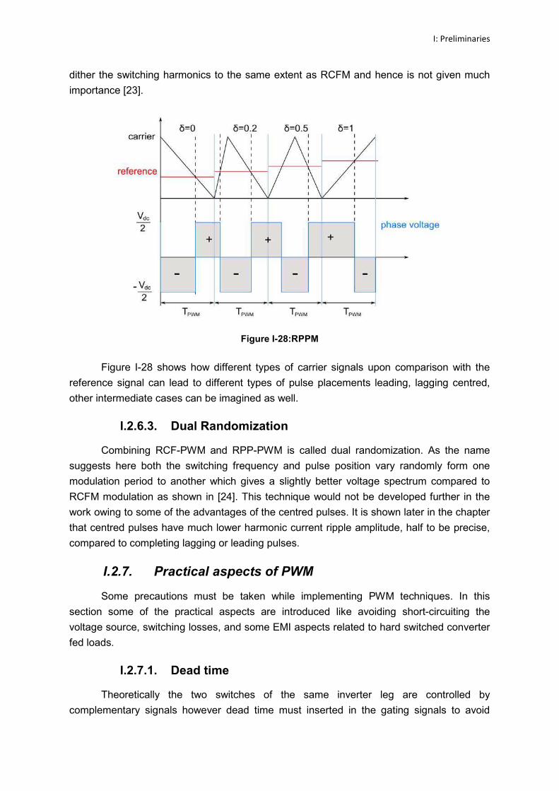
I: Preliminaries
dither the switching harmonics to the same extent as RCFM and hence is not given much
importance [23].
Figure I-28:RPPM
Figure I-28 shows how different types of carrier signals upon comparison with the
reference signal can lead to different types of pulse placements leading, lagging centred,
other intermediate cases can be imagined as well.
I.2.6.3. Dual Randomization
Combining RCF-PWM and RPP-PWM is called dual randomization. As the name
suggests here both the switching frequency and pulse position vary randomly form one
modulation period to another which gives a slightly better voltage spectrum compared to
RCFM modulation as shown in [24]. This technique would not be developed further in the
work owing to some of the advantages of the centred pulses. It is shown later in the chapter
that centred pulses have much lower harmonic current ripple amplitude, half to be precise,
compared to completing lagging or leading pulses.
I.2.7. Practical aspects of PWM
Some precautions must be taken while implementing PWM techniques. In this
section some of the practical aspects are introduced like avoiding short-circuiting the
voltage source, switching losses, and some EMI aspects related to hard switched converter
fed loads.
I.2.7.1. Dead time
Theoretically the two switches of the same inverter leg are controlled by
complementary signals however dead time must inserted in the gating signals to avoid
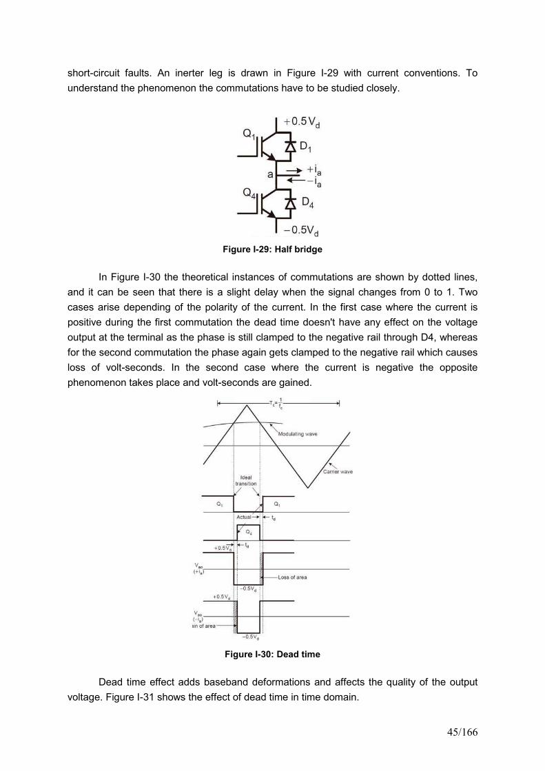
45/166
short-circuit faults. An inerter leg is drawn in Figure I-29 with current conventions. To
understand the phenomenon the commutations have to be studied closely.
Figure I-29: Half bridge
In Figure I-30 the theoretical instances of commutations are shown by dotted lines,
and it can be seen that there is a slight delay when the signal changes from 0 to 1. Two
cases arise depending of the polarity of the current. In the first case where the current is
positive during the first commutation the dead time doesn't have any effect on the voltage
output at the terminal as the phase is still clamped to the negative rail through D4, whereas
for the second commutation the phase again gets clamped to the negative rail which causes
loss of volt-seconds. In the second case where the current is negative the opposite
phenomenon takes place and volt-seconds are gained.
Figure I-30: Dead time
Dead time effect adds baseband deformations and affects the quality of the output
voltage. Figure I-31 shows the effect of dead time in time domain.
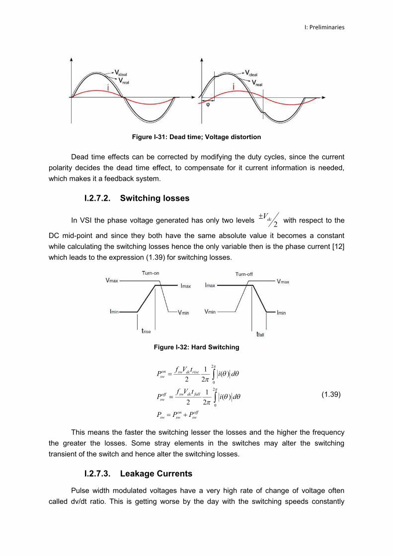
I: Preliminaries
Figure I-31: Dead time; Voltage distortion
Dead time effects can be corrected by modifying the duty cycles, since the current
polarity decides the dead time effect, to compensate for it current information is needed,
which makes it a feedback system.
I.2.7.2. Switching losses
In VSI the phase voltage generated has only two levels 2dcV with respect to the
DC mid-point and since they both have the same absolute value it becomes a constant
while calculating the switching losses hence the only variable then is the phase current [12]
which leads to the expression (1.39) for switching losses.
Figure I-32: Hard Switching
2
0
2
0
1( )
2 2
1( )
2 2
on sw dc risesw
sw dc falloff
sw
on off
sw sw sw
f V tP i d
f V tP i d
P P P
(1.39)
This means the faster the switching lesser the losses and the higher the frequency
the greater the losses. Some stray elements in the switches may alter the switching
transient of the switch and hence alter the switching losses.
I.2.7.3. Leakage Currents
Pulse width modulated voltages have a very high rate of change of voltage often
called dv/dt ratio. This is getting worse by the day with the switching speeds constantly
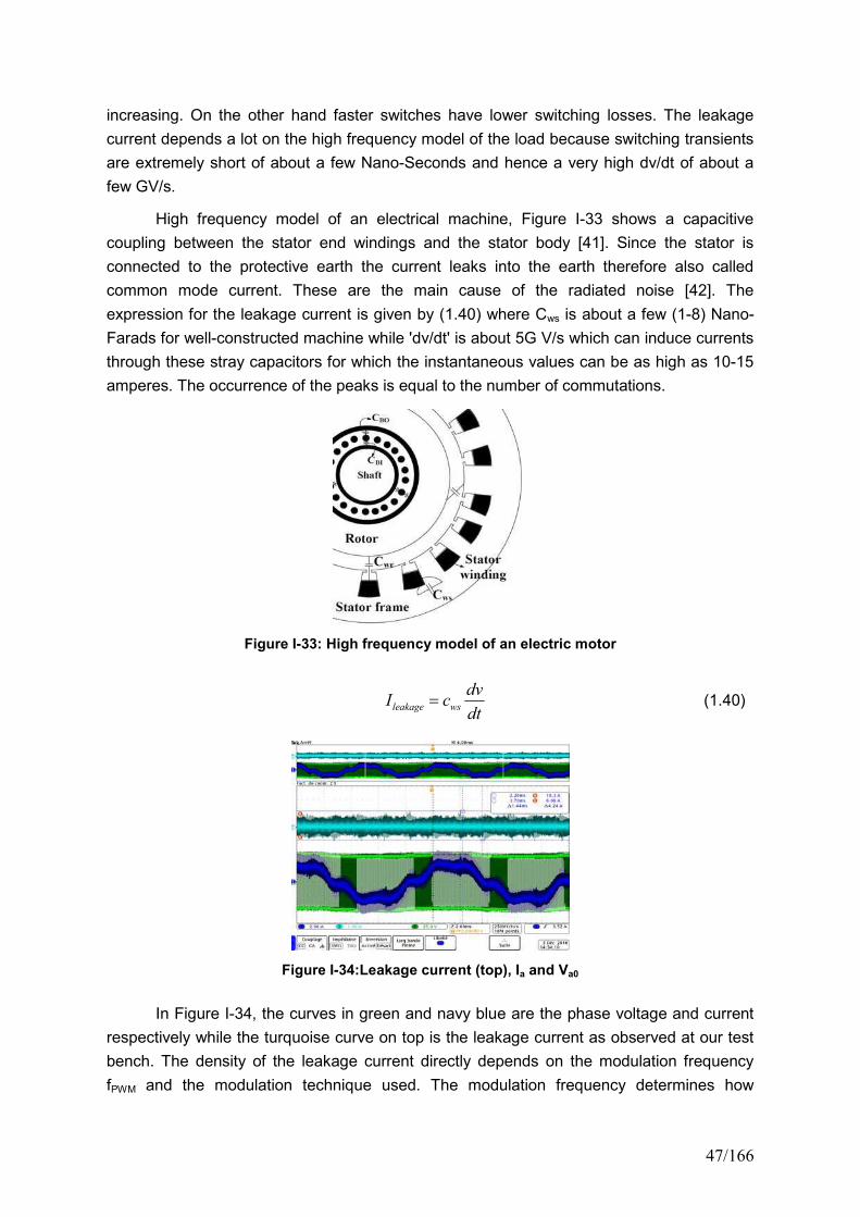
47/166
increasing. On the other hand faster switches have lower switching losses. The leakage
current depends a lot on the high frequency model of the load because switching transients
are extremely short of about a few Nano-Seconds and hence a very high dv/dt of about a
few GV/s.
High frequency model of an electrical machine, Figure I-33 shows a capacitive
coupling between the stator end windings and the stator body [41]. Since the stator is
connected to the protective earth the current leaks into the earth therefore also called
common mode current. These are the main cause of the radiated noise [42]. The
expression for the leakage current is given by (1.40) where Cws is about a few (1-8) Nano-
Farads for well-constructed machine while 'dv/dt' is about 5G V/s which can induce currents
through these stray capacitors for which the instantaneous values can be as high as 10-15
amperes. The occurrence of the peaks is equal to the number of commutations.
Figure I-33: High frequency model of an electric motor
leakage ws
dvI c
dt (1.40)
Figure I-34:Leakage current (top), Ia and Va0
In Figure I-34, the curves in green and navy blue are the phase voltage and current
respectively while the turquoise curve on top is the leakage current as observed at our test
bench. The density of the leakage current directly depends on the modulation frequency
fPWM and the modulation technique used. The modulation frequency determines how
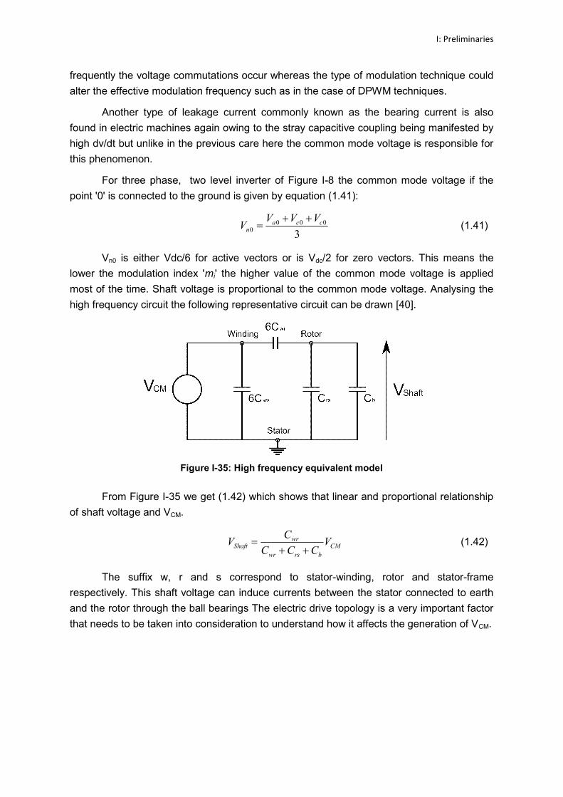
I: Preliminaries
frequently the voltage commutations occur whereas the type of modulation technique could
alter the effective modulation frequency such as in the case of DPWM techniques.
Another type of leakage current commonly known as the bearing current is also
found in electric machines again owing to the stray capacitive coupling being manifested by
high dv/dt but unlike in the previous care here the common mode voltage is responsible for
this phenomenon.
For three phase, two level inverter of Figure I-8 the common mode voltage if the
point '0' is connected to the ground is given by equation (1.41):
0 0 00 3
a c cn
V V VV
(1.41)
Vn0 is either Vdc/6 for active vectors or is Vdc/2 for zero vectors. This means the
lower the modulation index 'mi' the higher value of the common mode voltage is applied
most of the time. Shaft voltage is proportional to the common mode voltage. Analysing the
high frequency circuit the following representative circuit can be drawn [40].
Figure I-35: High frequency equivalent model
From Figure I-35 we get (1.42) which shows that linear and proportional relationship
of shaft voltage and VCM.
wrShaft CM
wr rs b
CV V
C C C (1.42)
The suffix w, r and s correspond to stator-winding, rotor and stator-frame
respectively. This shaft voltage can induce currents between the stator connected to earth
and the rotor through the ball bearings The electric drive topology is a very important factor
that needs to be taken into consideration to understand how it affects the generation of VCM.
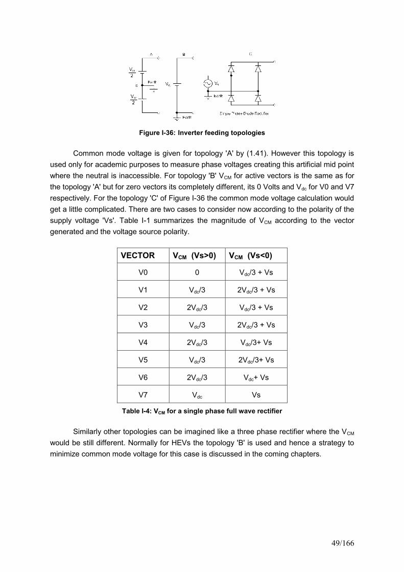
49/166
Figure I-36: Inverter feeding topologies
Common mode voltage is given for topology 'A' by (1.41). However this topology is
used only for academic purposes to measure phase voltages creating this artificial mid point
where the neutral is inaccessible. For topology 'B' VCM for active vectors is the same as for
the topology 'A' but for zero vectors its completely different, its 0 Volts and Vdc for V0 and V7
respectively. For the topology 'C' of Figure I-36 the common mode voltage calculation would
get a little complicated. There are two cases to consider now according to the polarity of the
supply voltage 'Vs'. Table I-1 summarizes the magnitude of VCM according to the vector
generated and the voltage source polarity.
VECTOR VCM (Vs>0) VCM (Vs<0)
V0 0 Vdc/3 + Vs
V1 Vdc/3 2Vdc/3 + Vs
V2 2Vdc/3 Vdc/3 + Vs
V3 Vdc/3 2Vdc/3 + Vs
V4 2Vdc/3 Vdc/3+ Vs
V5 Vdc/3 2Vdc/3+ Vs
V6 2Vdc/3 Vdc+ Vs
V7 Vdc Vs
Table I-4: VCM for a single phase full wave rectifier
Similarly other topologies can be imagined like a three phase rectifier where the VCMwould be still different. Normally for HEVs the topology 'B' is used and hence a strategy to
minimize common mode voltage for this case is discussed in the coming chapters.
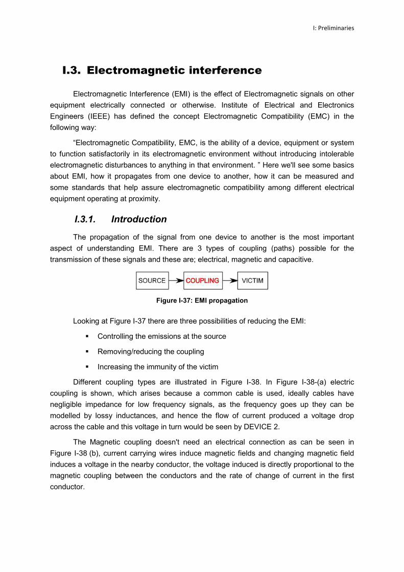
I: Preliminaries
I.3. Electromagnetic interference
Electromagnetic Interference (EMI) is the effect of Electromagnetic signals on other
equipment electrically connected or otherwise. Institute of Electrical and Electronics
Engineers (IEEE) has defined the concept Electromagnetic Compatibility (EMC) in the
following way:
“Electromagnetic Compatibility, EMC, is the ability of a device, equipment or system
to function satisfactorily in its electromagnetic environment without introducing intolerable
electromagnetic disturbances to anything in that environment. ” Here we'll see some basics
about EMI, how it propagates from one device to another, how it can be measured and
some standards that help assure electromagnetic compatibility among different electrical
equipment operating at proximity.
I.3.1. Introduction
The propagation of the signal from one device to another is the most important
aspect of understanding EMI. There are 3 types of coupling (paths) possible for the
transmission of these signals and these are; electrical, magnetic and capacitive.
Figure I-37: EMI propagation
Looking at Figure I-37 there are three possibilities of reducing the EMI:
Controlling the emissions at the source
Removing/reducing the coupling
Increasing the immunity of the victim
Different coupling types are illustrated in Figure I-38. In Figure I-38-(a) electric
coupling is shown, which arises because a common cable is used, ideally cables have
negligible impedance for low frequency signals, as the frequency goes up they can be
modelled by lossy inductances, and hence the flow of current produced a voltage drop
across the cable and this voltage in turn would be seen by DEVICE 2.
The Magnetic coupling doesn't need an electrical connection as can be seen in
Figure I-38 (b), current carrying wires induce magnetic fields and changing magnetic field
induces a voltage in the nearby conductor, the voltage induced is directly proportional to the
magnetic coupling between the conductors and the rate of change of current in the first
conductor.
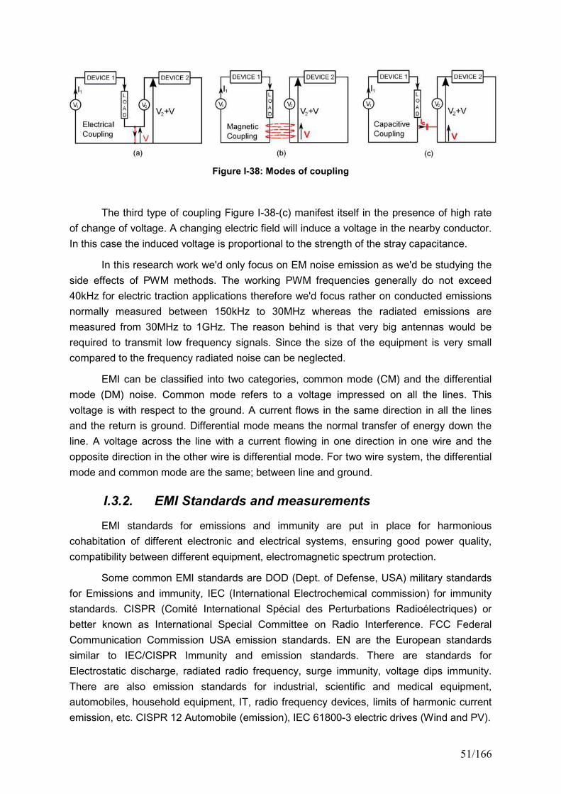
51/166
Figure I-38: Modes of coupling
The third type of coupling Figure I-38-(c) manifest itself in the presence of high rate
of change of voltage. A changing electric field will induce a voltage in the nearby conductor.
In this case the induced voltage is proportional to the strength of the stray capacitance.
In this research work we'd only focus on EM noise emission as we'd be studying the
side effects of PWM methods. The working PWM frequencies generally do not exceed
40kHz for electric traction applications therefore we'd focus rather on conducted emissions
normally measured between 150kHz to 30MHz whereas the radiated emissions are
measured from 30MHz to 1GHz. The reason behind is that very big antennas would be
required to transmit low frequency signals. Since the size of the equipment is very small
compared to the frequency radiated noise can be neglected.
EMI can be classified into two categories, common mode (CM) and the differential
mode (DM) noise. Common mode refers to a voltage impressed on all the lines. This
voltage is with respect to the ground. A current flows in the same direction in all the lines
and the return is ground. Differential mode means the normal transfer of energy down the
line. A voltage across the line with a current flowing in one direction in one wire and the
opposite direction in the other wire is differential mode. For two wire system, the differential
mode and common mode are the same; between line and ground.
I.3.2. EMI Standards and measurements
EMI standards for emissions and immunity are put in place for harmonious
cohabitation of different electronic and electrical systems, ensuring good power quality,
compatibility between different equipment, electromagnetic spectrum protection.
Some common EMI standards are DOD (Dept. of Defense, USA) military standards
for Emissions and immunity, IEC (International Electrochemical commission) for immunity
standards. CISPR (Comité International Spécial des Perturbations Radioélectriques) or
better known as International Special Committee on Radio Interference. FCC Federal
Communication Commission USA emission standards. EN are the European standards
similar to IEC/CISPR Immunity and emission standards. There are standards for
Electrostatic discharge, radiated radio frequency, surge immunity, voltage dips immunity.
There are also emission standards for industrial, scientific and medical equipment,
automobiles, household equipment, IT, radio frequency devices, limits of harmonic current
emission, etc. CISPR 12 Automobile (emission), IEC 61800-3 electric drives (Wind and PV).
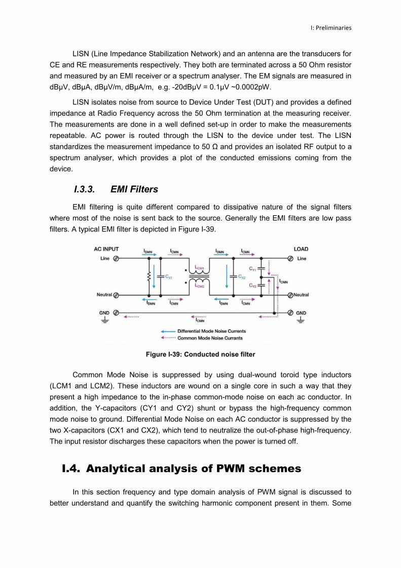
I: Preliminaries
LISN (Line Impedance Stabilization Network) and an antenna are the transducers for
CE and RE measurements respectively. They both are terminated across a 50 Ohm resistor
and measured by an EMI receiver or a spectrum analyser. The EM signals are measured in
dBµV, dBµA, dBµV/m, dBµA/m, e.g. -20dBµV = 0.1µV ~0.0002pW.
LISN isolates noise from source to Device Under Test (DUT) and provides a defined
impedance at Radio Frequency across the 50 Ohm termination at the measuring receiver.
The measurements are done in a well defined set-up in order to make the measurements
repeatable. AC power is routed through the LISN to the device under test. The LISN
standardizes the measurement impedance to 50 Ω and provides an isolated RF output to a spectrum analyser, which provides a plot of the conducted emissions coming from the
device.
I.3.3. EMI Filters
EMI filtering is quite different compared to dissipative nature of the signal filters
where most of the noise is sent back to the source. Generally the EMI filters are low pass
filters. A typical EMI filter is depicted in Figure I-39.
Figure I-39: Conducted noise filter
Common Mode Noise is suppressed by using dual-wound toroid type inductors
(LCM1 and LCM2). These inductors are wound on a single core in such a way that they
present a high impedance to the in-phase common-mode noise on each ac conductor. In
addition, the Y-capacitors (CY1 and CY2) shunt or bypass the high-frequency common
mode noise to ground. Differential Mode Noise on each AC conductor is suppressed by the
two X-capacitors (CX1 and CX2), which tend to neutralize the out-of-phase high-frequency.
The input resistor discharges these capacitors when the power is turned off.
I.4. Analytical analysis of PWM schemes
In this section frequency and type domain analysis of PWM signal is discussed to
better understand and quantify the switching harmonic component present in them. Some
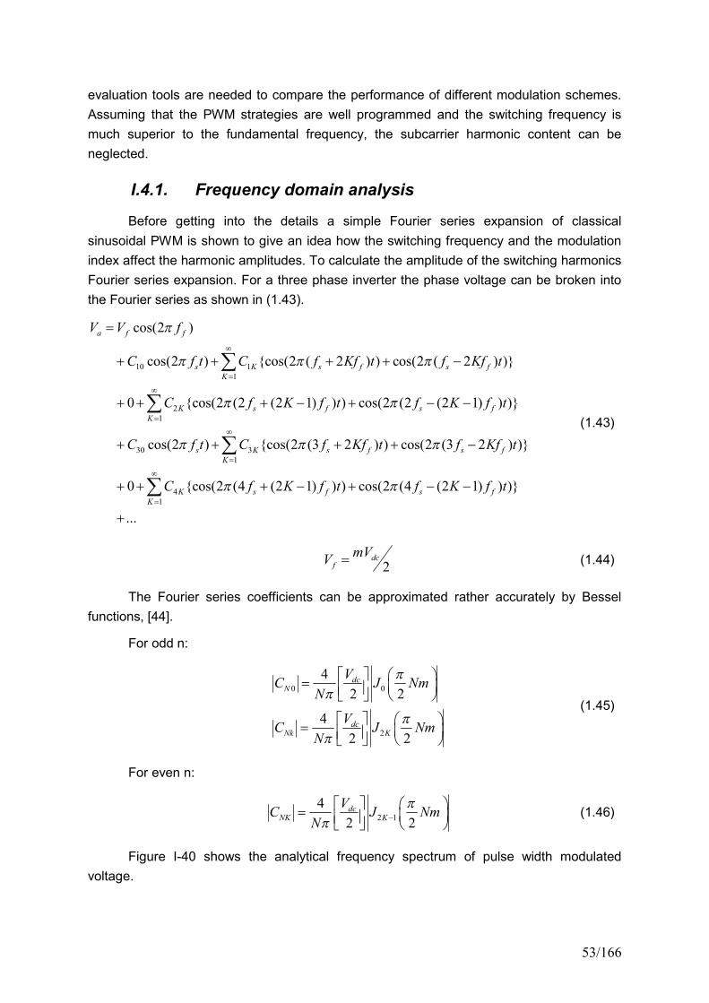
53/166
evaluation tools are needed to compare the performance of different modulation schemes.
Assuming that the PWM strategies are well programmed and the switching frequency is
much superior to the fundamental frequency, the subcarrier harmonic content can be
neglected.
I.4.1. Frequency domain analysis
Before getting into the details a simple Fourier series expansion of classical
sinusoidal PWM is shown to give an idea how the switching frequency and the modulation
index affect the harmonic amplitudes. To calculate the amplitude of the switching harmonics
Fourier series expansion. For a three phase inverter the phase voltage can be broken into
the Fourier series as shown in (1.43).
10 11
21
30 31
4
cos(2 )
cos(2 ) {cos(2 ( 2 ) ) cos(2 ( 2 ) )}
0 {cos(2 (2 (2 1) ) ) cos(2 (2 (2 1) ) )}
cos(2 ) {cos(2 (3 2 ) ) cos(2 (3 2 ) )}
0
a f f
s K s f s f
K
K s f s f
K
s K s f s f
K
K
V V f
C f t C f Kf t f Kf t
C f K f t f K f t
C f t C f Kf t f Kf t
C
1
{cos(2 (4 (2 1) ) ) cos(2 (4 (2 1) ) )}
...
s f s f
K
f K f t f K f t
(1.43)
2dc
f
mVV (1.44)
The Fourier series coefficients can be approximated rather accurately by Bessel
functions, [44].
For odd n:
0 0
2
4
2 2
4
2 2
dcN
dcNk K
VC J Nm
N
VC J Nm
N
(1.45)
For even n:
2 1
4
2 2dc
NK K
VC J Nm
N
(1.46)
Figure I-40 shows the analytical frequency spectrum of pulse width modulated
voltage.

I: Preliminaries
Figure I-40: Frequency Spectrum: PWM
Figure I-41 shows the carrier first five harmonic amplitudes with respect to the
modulation depth, it can be observed that for higher modulation index the amplitudes
decrease considerably specially for the first carrier harmonic.
Figure I-41: Carrier Harmonic Amplitudes
Figure I-42 shows the how the sideband harmonic dependence on the harmonic
number and the modulation index. It is clear from the graphic that for higher harmonic
number and high modulation index the amplitudes decrease.
Figure I-42: Sideband Harmonic Amplitudes
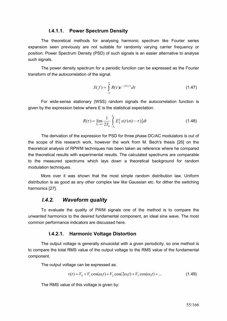
55/166
I.4.1.1. Power Spectrum Density
The theoretical methods for analysing harmonic spectrum like Fourier series
expansion seen previously are not suitable for randomly varying carrier frequency or
position. Power Spectrum Density (PSD) of such signals is an easier alternative to analyse
such signals.
The power density spectrum for a periodic function can be expressed as the Fourier
transform of the autocorrelation of the signal.
2( ) ( ) j fS f R e d
(1.47)
For wide-sense stationary (WSS) random signals the autocorrelation function is
given by the expression below where E is the statistical expectation.
0
000
1( ) lim ( ) ( )
2
T
TT
R E x t x t dtT
(1.48)
The derivation of the expression for PSD for three phase DC/AC modulators is out of
the scope of this research work, however the work from M. Bech's thesis [26] on the
theoretical analysis of RPWM techniques has been taken as reference where he compared
the theoretical results with experimental results. The calculated spectrums are comparable
to the measured spectrums which lays down a theoretical background for random
modulation techniques.
More over it was shown that the most simple random distribution law, Uniform
distribution is as good as any other complex law like Gaussian etc. for dither the switching
harmonics [27].
I.4.2. Waveform quality
To evaluate the quality of PWM signals one of the method is to compare the
unwanted harmonics to the desired fundamental component, an ideal sine wave. The most
common performance indicators are discussed here.
I.4.2.1. Harmonic Voltage Distortion
The output voltage is generally sinusoidal with a given periodicity, so one method is
to compare the total RMS value of the output voltage to the RMS value of the fundamental
component.
The output voltage can be expressed as:
0 1 1 2 1 3 3( ) cos( ) cos(2 ) cos( ) ...v t V V t V t V t (1.49)
The RMS value of this voltage is given by:
I: Preliminaries
2
0
1 10 00
1( )
1cos( )cos( )
T
RMS
T
n k
n k
V v t dtT
V V n t k t dtT
(1.50)
From (1.51) it can be readily seen that for n≠k the integral over a complete period would be zero and for n=k the integral comes out to be ½.
1cos( )cos( ) {cos[( ) ] cos[( ) ]}
2n t k t n k t n k t (1.51)
Normally such voltages don't have a DC and even harmonic components and can be
reduced to:
2
1,3,5... 2n
RMS
n
VV
(1.52)
From which:
2,
1,3,5...RMS n RMS
n
V V
(1.53)
The total RMS value can be rewritten factoring the desired term, usually the
fundamental component as:
2,
1, 23,5,7... 1,
21,
1
1
n RMS
RMS RMS
n RMS
RMS
VV V
V
V THD
(1.54)
From where the unwanted components termed as total harmonic distortion (THD) is:
2,2
3,5,7... 1,
2
23,5,7... 1
n RMS
n RMS
n
n
VTHD
V
V
V
(1.55)
Or the THD can be expressed as:
2
1,
( ) 1RMS
RMS
VTHD
V (1.56)
A square wave voltage output can be expanded as:
57/166
2 1 1 1( ) cos cos3 cos5 cos7 ...
3 5 7dc
sqw
Vv t t t t t
(1.57)
It should be noted that the third order harmonics disappear for three phase inverters,
so the output voltage is less distorted.
23,5,7,...
2
1
18
sqw
n
THDn
(1.58)
Till now we discussed the output voltage quality of the inverter which makes sense
as it is the quantity which is controlled by the PWM. However it is the current that is of more
interest for loss, torque ripple, output power calculations and hence calculating the current
harmonic distortion THDi may be more useful. Current depends on the load characteristics
and therefore cannot be known before hand, however in many applications the load can be
modelled by a lossy inductance, e.g. electric motors. Then the current harmonics can be
given by:
nn
VI
n L (1.59)
2
2
2
2
1
ni
n
n
n
VTHD
n L
V
L n
(1.60)
To get rid of the inductance this THDi can be normalised with respect to I1, the
fundamental component of the current, this quantity is known is as weighted total harmonic
distortion (WTHD).
2
2
1
n
n
V
nWTHD
V
(1.61)
The WTHD for the square wave of equation (1.57) can be calculated in a similar
manner and is given by (1.62).
43,5,7,...
1
0.1212
sqw
n
WTHDn
(1.62)
There is a serious limitation to THD as a yardstick to compare different PWM
methods as the RMS value used for the calculation is the same for all being equal to Vdc.
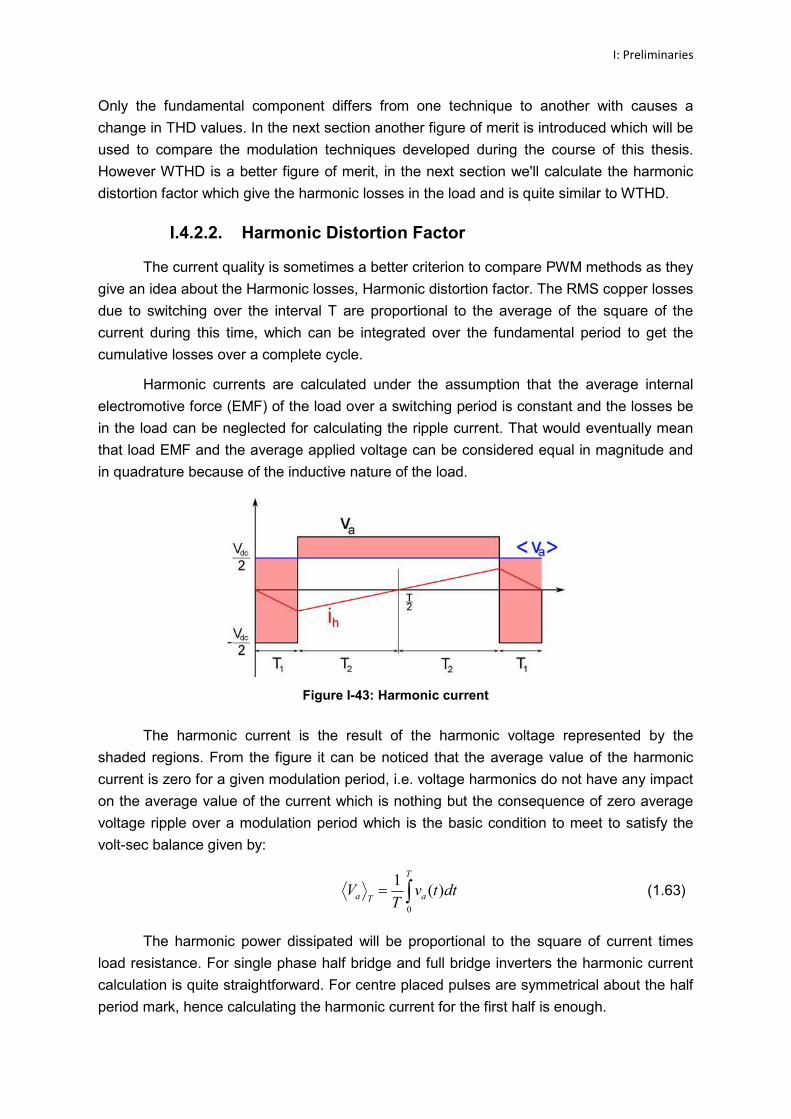
I: Preliminaries
Only the fundamental component differs from one technique to another with causes a
change in THD values. In the next section another figure of merit is introduced which will be
used to compare the modulation techniques developed during the course of this thesis.
However WTHD is a better figure of merit, in the next section we'll calculate the harmonic
distortion factor which give the harmonic losses in the load and is quite similar to WTHD.
I.4.2.2. Harmonic Distortion Factor
The current quality is sometimes a better criterion to compare PWM methods as they
give an idea about the Harmonic losses, Harmonic distortion factor. The RMS copper losses
due to switching over the interval T are proportional to the average of the square of the
current during this time, which can be integrated over the fundamental period to get the
cumulative losses over a complete cycle.
Harmonic currents are calculated under the assumption that the average internal
electromotive force (EMF) of the load over a switching period is constant and the losses be
in the load can be neglected for calculating the ripple current. That would eventually mean
that load EMF and the average applied voltage can be considered equal in magnitude and
in quadrature because of the inductive nature of the load.
Figure I-43: Harmonic current
The harmonic current is the result of the harmonic voltage represented by the
shaded regions. From the figure it can be noticed that the average value of the harmonic
current is zero for a given modulation period, i.e. voltage harmonics do not have any impact
on the average value of the current which is nothing but the consequence of zero average
voltage ripple over a modulation period which is the basic condition to meet to satisfy the
volt-sec balance given by:
0
1( )
T
a aTV v t dt
T (1.63)
The harmonic power dissipated will be proportional to the square of current times
load resistance. For single phase half bridge and full bridge inverters the harmonic current
calculation is quite straightforward. For centre placed pulses are symmetrical about the half
period mark, hence calculating the harmonic current for the first half is enough.
59/166
1
1 2
( )( )
: ( ) 02
( ) 2
a a
h
dca
dca
v t vi t t
L
VWhere v t for t T
Vand v t forT t T
(1.64)
From the figure it can be seen that at T/2 the harmonic becomes zero:
2( ) 0hi T (1.65)
With the help of equation (1.64) and (1.65):
1 1
2 1 2
( ) ( 1 )2
( ) [( 1 ) (1 ) ]22
:
dch
dch
a
dc
Vi T u T
L
Vi T u T u T
L
vWhere u
V
(1.66)
From equation (1.65) and (1.66) T1 and T2 can be expressed in terms of
1 2
1 2
2(1 ) (1 )
4 4
TT T
u T u TT andT
(1.67)
The average square value of the ripple current can be found out by integrating the
squared value over the entire period.
1 1 2
1
22 2 2 2
1 1
0
2(1 ) [( 1 ) (1 )( )]
2
T T T
dch T
T
Vi u t dt u T u t T dt
L T
(1.68)
Simplifying it gives the following expression:
2 2 2 22 (1 )
2 48dc
hT
V T ui
L
(1.69)
The term 'u' can also be written as:
12 2 cos
4cos
a
dc dc
i
v Au
V V
m
(1.70)
So the average harmonic loss over a fundamental period can be calculated as
follows:
I: Preliminaries
2 2222 2 2
0
41 cos
2 48dc
h i
V Ti m d
L
(1.71)
That upon solving reduces to:
2 22 2 44 3
12 48 2dc
h i i
V Ti m m
L (1.72)
To compare different topologies irrespective of the switching frequency and the DC
link voltage, harmonic distortion function can be introduced as:
2 44 3( ) 1
2i i if m m m (1.73)
Similarly the harmonic distortion function can be calculated for other inverter
topologies. For full phase single bridge configuration is given by:
2 3 42
8 128 6( )
3i i i if m m m m (1.74)
Under similar hypothesis HDF can be calculated for three phase PWM techniques,
the expression for the harmonic current becomes (1.75).
2 2 3 3 322 1 2 1 2 1 2 12
( ) ( ) ( )( )
48dc
hT
T u u u u u u u uVi
L
(1.75)
The results for some of the techniques mentioned in the previous section are shown
here, [16]. Equation (1.76) gives the HDF for the most basic modulation scheme, i.e. the
sinusoidal modulation scheme where m varies from 0 to 0.785.
2 3 44 3 4 3 9( )
2 8SPWM i i i if m m m m (1.76)
Similarly for one-sixth and one-quarter third harmonic injection THIPWM1/6 and
THIPWM1/4 are given by (1.77) and (1.78) respectively. The maximum value of the
modulation index for THIPWM1/4 is slightly less than 0.907 which is the maximum possible
value.
2 3 41/ 6
4 3 4 3( )
2THIPWM i i i if m m m m (1.77)
2 3 41/ 4
4 3 4 3 63( )
2 64THIPWM i i i if m m m m (1.78)
HDF for SVM and SVPWM are given by (1.79).
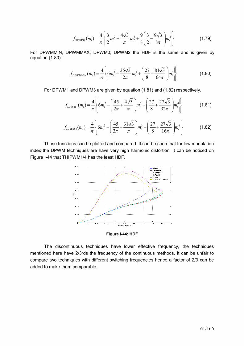
61/166
2 3 44 3 4 3 9 3 9 3( )
2 8 2 8SVPWM i i I if m m m m (1.79)
For DPWMMIN, DPWMMAX, DPWM0, DPWM2 the HDF is the same and is given byequation (1.80).
2 3 44 35 3 27 81 3( ) 6
2 8 64DPWMMIN i i i if m m m m (1.80)
For DPWM1 and DPWM3 are given by equation (1.81) and (1.82) respectively.
2 3 41
4 45 4 3 27 27 3( ) 6
2 8 32DPWM i i i if m m m m (1.81)
2 3 43
4 45 31 3 27 27 3( ) 6
2 8 16DPWM i i i if m m m m (1.82)
These functions can be plotted and compared. It can be seen that for low modulation
index the DPWM techniques are have very high harmonic distortion. It can be noticed on
Figure I-44 that THIPWM1/4 has the least HDF.
Figure I-44: HDF
The discontinuous techniques have lower effective frequency, the techniques
mentioned here have 2/3rds the frequency of the continuous methods. It can be unfair to
compare two techniques with different switching frequencies hence a factor of 2/3 can be
added to make them comparable.
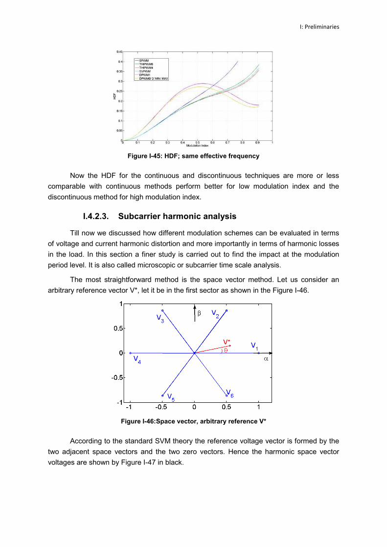
I: Preliminaries
Figure I-45: HDF; same effective frequency
Now the HDF for the continuous and discontinuous techniques are more or less
comparable with continuous methods perform better for low modulation index and the
discontinuous method for high modulation index.
I.4.2.3. Subcarrier harmonic analysis
Till now we discussed how different modulation schemes can be evaluated in terms
of voltage and current harmonic distortion and more importantly in terms of harmonic losses
in the load. In this section a finer study is carried out to find the impact at the modulation
period level. It is also called microscopic or subcarrier time scale analysis.
The most straightforward method is the space vector method. Let us consider an
arbitrary reference vector V*, let it be in the first sector as shown in the Figure I-46.
Figure I-46:Space vector, arbitrary reference V*
According to the standard SVM theory the reference voltage vector is formed by the
two adjacent space vectors and the two zero vectors. Hence the harmonic space vector
voltages are shown by Figure I-47 in black.

63/166
Figure I-47: Harmonic voltage vectors
Under the same assumptions as earlier i.e. considering the load as purely inductive.
The harmonic currents can be calculated by the following expression (1.83), where Vj is the
adjacent space vector.
*
0
1( )
T
h ji V V dtL
(1.83)
From the above expression it is obvious that the harmonic current depends on the
reference vector, hence on mi and θ, as well as the space vectors. For standard SVMimplementation the sequence of vector application is 0127-7210 as shown in Figure I-48.
Figure I-48: SVM switching sequence
So a total of four vectors are used and for sector one these are V0, V1, V2, and V7.
To get rid of the load inductance value harmonic flux can be calculated instead by
multiplying equation (1.83) by L. Harmonic flux for all of these vectors is given by (1.84).
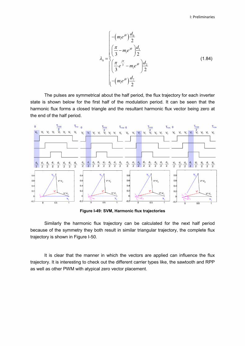
I: Preliminaries
0
1
23
7
2
3 2
3 2
2
j
i
j
i
h j
j
i
j
i
dme
dme
de m e
dme
(1.84)
The pulses are symmetrical about the half period, the flux trajectory for each inverter
state is shown below for the first half of the modulation period. It can be seen that the
harmonic flux forms a closed triangle and the resultant harmonic flux vector being zero at
the end of the half period.
Figure I-49: SVM, Harmonic flux trajectories
Similarly the harmonic flux trajectory can be calculated for the next half period
because of the symmetry they both result in similar triangular trajectory, the complete flux
trajectory is shown in Figure I-50.
It is clear that the manner in which the vectors are applied can influence the flux
trajectory. It is interesting to check out the different carrier types like, the sawtooth and RPP
as well as other PWM with atypical zero vector placement.
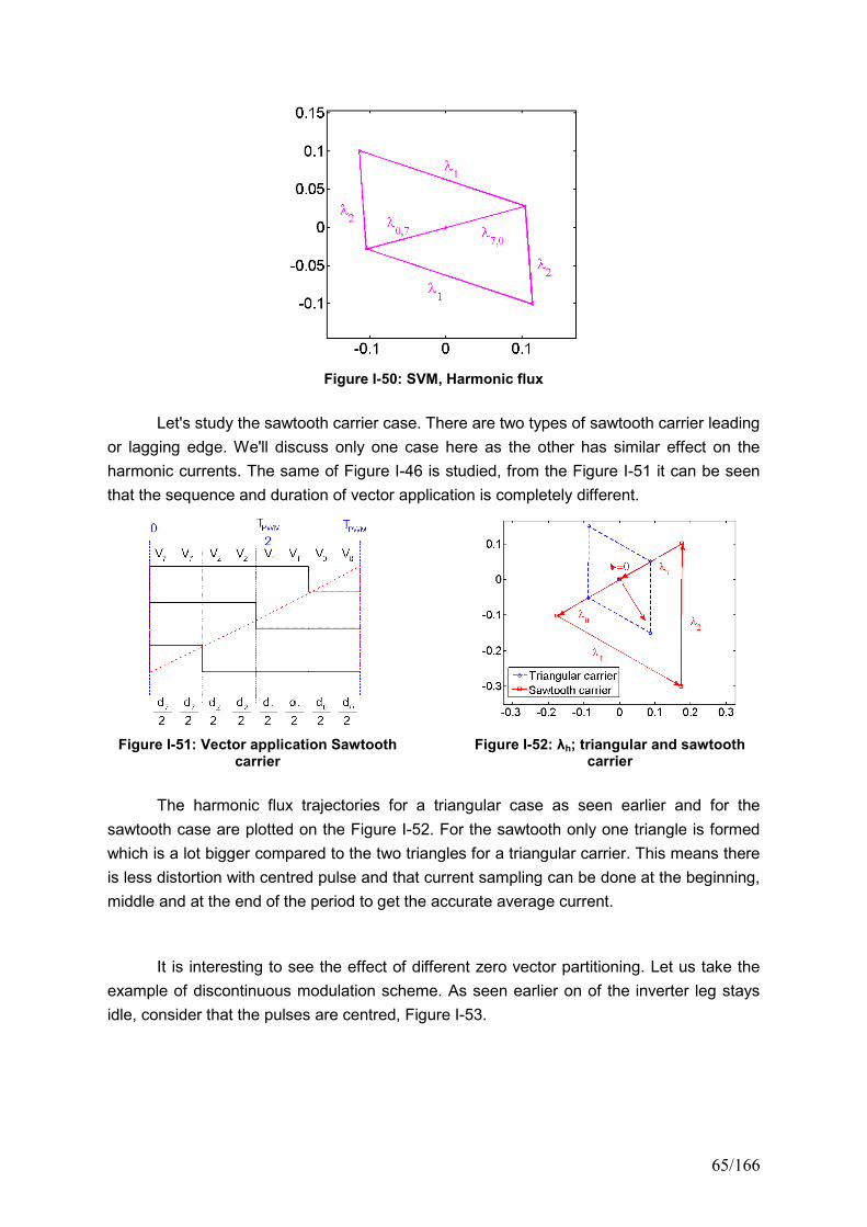
65/166
Figure I-50: SVM, Harmonic flux
Let's study the sawtooth carrier case. There are two types of sawtooth carrier leading
or lagging edge. We'll discuss only one case here as the other has similar effect on the
harmonic currents. The same of Figure I-46 is studied, from the Figure I-51 it can be seen
that the sequence and duration of vector application is completely different.
Figure I-51: Vector application Sawtoothcarrier
Figure I-52: λh; triangular and sawtoothcarrier
The harmonic flux trajectories for a triangular case as seen earlier and for the
sawtooth case are plotted on the Figure I-52. For the sawtooth only one triangle is formed
which is a lot bigger compared to the two triangles for a triangular carrier. This means there
is less distortion with centred pulse and that current sampling can be done at the beginning,
middle and at the end of the period to get the accurate average current.
It is interesting to see the effect of different zero vector partitioning. Let us take the
example of discontinuous modulation scheme. As seen earlier on of the inverter leg stays
idle, consider that the pulses are centred, Figure I-53.
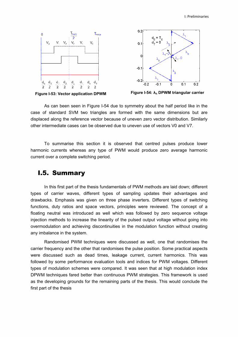
I: Preliminaries
Figure I-53: Vector application DPWM Figure I-54: λh DPWM triangular carrier
As can been seen in Figure I-54 due to symmetry about the half period like in the
case of standard SVM two triangles are formed with the same dimensions but are
displaced along the reference vector because of uneven zero vector distribution. Similarly
other intermediate cases can be observed due to uneven use of vectors V0 and V7.
To summarise this section it is observed that centred pulses produce lower
harmonic currents whereas any type of PWM would produce zero average harmonic
current over a complete switching period.
I.5. Summary
In this first part of the thesis fundamentals of PWM methods are laid down; different
types of carrier waves, different types of sampling updates their advantages and
drawbacks. Emphasis was given on three phase inverters. Different types of switching
functions, duty ratios and space vectors, principles were reviewed. The concept of a
floating neutral was introduced as well which was followed by zero sequence voltage
injection methods to increase the linearity of the pulsed output voltage without going into
overmodulation and achieving discontinuities in the modulation function without creating
any imbalance in the system.
Randomised PWM techniques were discussed as well, one that randomises the
carrier frequency and the other that randomises the pulse position. Some practical aspects
were discussed such as dead times, leakage current, current harmonics. This was
followed by some performance evaluation tools and indices for PWM voltages. Different
types of modulation schemes were compared. It was seen that at high modulation index
DPWM techniques fared better than continuous PWM strategies. This framework is used
as the developing grounds for the remaining parts of the thesis. This would conclude the
first part of the thesis

67/166
PART II
DEVELOPMENT OF PWM
SCHEMES

II: Development of PWM Schemes
II. Development of PWM Schemes
In the previous chapter the fundamentals of PWM, the state of art was discussed to
prepare ground for further development of PWM techniques. In this chapter some new
PWM techniques developed for the thesis are presented and a comparison with the
existing methods is made, these techniques can be classified into discontinuous,
randomized modulators and two other modulation techniques that can optimise the
number of current sensors and the DC-link capacitor. All of these techniques are based on
space vector representation and calculation.
II.1. Introduction
In order to meet the objectives of this research several different issues are dealt
separately, one at a time. The issue of switching losses is dealt by introducing an
innovative discontinuous modulator. To reduce the filtering effort and hence avoid the use
of bulky EMI filters a random modulator is proposed. We know that the DC-link capacitors
can amount to up to 50% of the inverter volume. A technique to reduce it has been put
forward too.
In the first section of this chapter we'd do an in depth analysis of the degree of
freedom related to the floating neutral loads to be able to develop a PWM strategy to
minimise the switching losses. A generalised technique is presented which can adapt itself
to the different types of load characteristics to optimise losses in the inverter. In the second
part randomisation of PWM techniques looked into details and a randomised technique
best suited under given conditions is proposed which is analogous to a RCF modulator.
This is followed by techniques to reduce the number of current sensors required to perform
a vector control on AC machines and a technique to reduce the inverter input current
component which is directly related to the DC-link capacitor size.
II.2.Discontinuous Space Vector Modulation
We saw we could achieve discontinuous modulation strategies upon injecting a
zero sequence component in the voltage. On the other hand using space vector
calculations it becomes easier, the following example will make it clearer. For SVM we
calculate the active vector (Vi, Vj) duty cycles (Ti, Tj) and then complete it with the two
zero vectors (V0, V7) with equal participation, which gives the following sequence
V0→Vi→Vj→V7→V7→Vj→Vi→V0. Now if T0≠T7 and we consider the two extreme cases where T0=0 and T7=Tzero or T7=0 or T0=Tzero, where Tzero = TPWM-(Ti+Tj). These two case
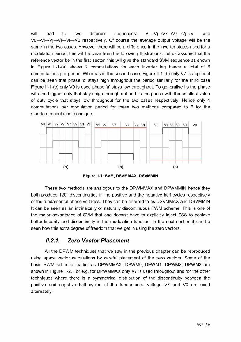
69/166
will lead to two different sequences; Vi→Vj→V7→V7→Vj→Vi and V0→Vi→Vj→Vj→Vi→V0 respectively. Of course the average output voltage will be the same in the two cases. However there will be a difference in the inverter states used for a
modulation period, this will be clear from the following illustrations. Let us assume that the
reference vector be in the first sector, this will give the standard SVM sequence as shown
in Figure II-1-(a) shows 2 commutations for each inverter leg hence a total of 6
commutations per period. Whereas in the second case, Figure II-1-(b) only V7 is applied it
can be seen that phase 'c' stays high throughout the period similarly for the third case
Figure II-1-(c) only V0 is used phase 'a' stays low throughout. To generalise its the phase
with the biggest duty that stays high through out and its the phase with the smallest value
of duty cycle that stays low throughout for the two cases respectively. Hence only 4
commutations per modulation period for these two methods compared to 6 for the
standard modulation technique.
Figure II-1: SVM, DSVMMAX, DSVMMIN
These two methods are analogous to the DPWMMAX and DPWMMIN hence they
both produce 120° discontinuities in the positive and the negative half cycles respectively
of the fundamental phase voltages. They can be referred to as DSVMMAX and DSVMMIN
It can be seen as an intrinsically or naturally discontinuous PWM scheme. This is one of
the major advantages of SVM that one doesn't have to explicitly inject ZSS to achieve
better linearity and discontinuity in the modulation function. In the next section it can be
seen how this extra degree of freedom that we get in using the zero vectors.
II.2.1. Zero Vector Placement
All the DPWM techniques that we saw in the previous chapter can be reproduced
using space vector calculations by careful placement of the zero vectors. Some of the
basic PWM schemes earlier as DPWMMAX, DPWM0, DPWM1, DPWM2, DPWM3 are
shown in Figure II-2. For e.g. for DPWMMAX only V7 is used throughout and for the other
techniques where there is a symmetrical distribution of the discontinuity between the
positive and negative half cycles of the fundamental voltage V7 and V0 are used
alternately.
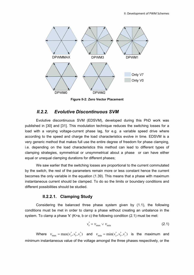
II: Development of PWM Schemes
Figure II-2: Zero Vector Placement
II.2.2. Evolutive Discontinuous SVM
Evolutive discontinuous SVM (EDSVM), developed during this PhD work was
published in [30] and [31]. This modulation technique reduces the switching losses for a
load with a varying voltage-current phase lag, for e.g. a variable speed drive where
according to the speed and charge the load characteristics evolve in time. EDSVM is a
very generic method that makes full use the entire degree of freedom for phase clamping,
i.e. depending on the load characteristics this method can lead to different types of
clamping strategies, symmetrical or unsymmetrical about a phase or can have either
equal or unequal clamping durations for different phases;
We saw earlier that the switching losses are proportional to the current commutated
by the switch, the rest of the parameters remain more or less constant hence the current
becomes the only variable in the equation (1.39). This means that a phase with maximum
instantaneous current should be clamped. To do so the limits or boundary conditions and
different possibilities should be studied.
II.2.2.1. Clamping Study
Considering the balanced three phase system given by (1.1), the following
conditions must be met in order to clamp a phase without creating an unbalance in the
system. To clamp a phase 'k' (K=a, b or c) the following condition (2.1) must be met:
*max minkv v v (2.1)
Where * * *max max( , , )a b cv v vv and * * *
min min( , , )a b cv v vv is the maximum and
minimum instantaneous value of the voltage amongst the three phases respectively, or the
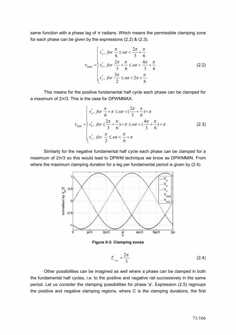
71/166
same function with a phase lag of π radians. Which means the permissible clamping zone for each phase can be given by the expressions (2.2) & (2.3).
*
*
*
max
2,
6 3 62 4
,3 6 3 63
, 22 6
a
b
c
v for t
v for t
v for t
v
(2.2)
This means for the positive fundamental half cycle each phase can be clamped for
a maximum of 2π/3. This is the case for DPWMMAX.
*
*
*
min
2, ( )
6 3 62 4
, ( ) ( )3 6 3 6
,2 6
a
b
c
v for t
v for t
v for t
v
(2.3)
Similarly for the negative fundamental half cycle each phase can be clamped for a
maximum of 2π/3 so this would lead to DPWM technique we know as DPWMMIN. From where the maximum clamping duration for a leg per fundamental period is given by (2.4)
Figure II-3: Clamping zones
max
2
3cT (2.4)
Other possibilities can be imagined as well where a phase can be clamped in both
the fundamental half cycles, i.e. to the positive and negative rail successively in the same
period. Let us consider the clamping possibilities for phase 'a'. Expression (2.5) regroups
the positive and negative clamping regions, where C is the clamping durations, the first
II: Development of PWM Schemes
suffix is the phase and the second represents the positive or negative clamping, and T the
total duration.
_
_
_
2, ,
6 3 6
2,
6 3 6
a ve
a clamping
a ve
C for t
T or
C for t
(2.5)
From where we can say that they both are comprised in the same interval given by
(2.6).
_ _
2, 0,
3a ve a vewhere C C
(2.6)
All the existing DPWM techniques follow the condition given by equation (2.7).
Where 'k' is any arbitrary phase, which basically means that all the phases will have the
same total clamping duration.
_ _
2
3k ve k veC C
(2.7)
In addition to that DPWM0, DPWM1, DPWM2, DPWM3 equally distribute this time,
given by (2.8).
_ _ 3a ve a veC C
(2.8)
Whereas for DPWMMAX is given by (2.9) and for DPWMMIN it's given by (2.10).
_ _, 03a ve a veC C
(2.9)
_ _0,3a ve a veC C
(2.10)
This makes these two techniques unsymmetrical about a phase. In the next section
we'd try to exploit all the freedom to develop a technique to reduce the switching losses.
II.2.2.2. Switching loss reduction
The proposed DSVM algorithm allows minimizing the switching losses . The
simplest discontinuous SVM technique, referred to above as DSVMMIN, as the basic
technique to complement the generalized modulator in terms of the load angle φ. The DSVM Algorithm is very simple and intelligent with almost no extra burden on the
processor. First of all the duty cycles are calculated for the given reference voltages
(generated by the torque control algorithm for electric drives) using the algorithm
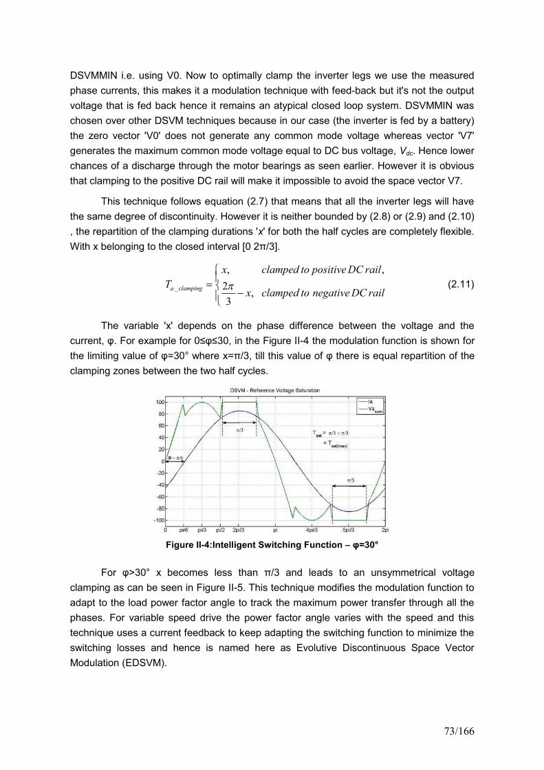
73/166
DSVMMIN i.e. using V0. Now to optimally clamp the inverter legs we use the measured
phase currents, this makes it a modulation technique with feed-back but it's not the output
voltage that is fed back hence it remains an atypical closed loop system. DSVMMIN was
chosen over other DSVM techniques because in our case (the inverter is fed by a battery)
the zero vector 'V0' does not generate any common mode voltage whereas vector 'V7'
generates the maximum common mode voltage equal to DC bus voltage, Vdc. Hence lower
chances of a discharge through the motor bearings as seen earlier. However it is obvious
that clamping to the positive DC rail will make it impossible to avoid the space vector V7.
This technique follows equation (2.7) that means that all the inverter legs will have
the same degree of discontinuity. However it is neither bounded by (2.8) or (2.9) and (2.10)
, the repartition of the clamping durations 'x' for both the half cycles are completely flexible.
With x belonging to the closed interval [0 2π/3].
_
, ,
2,
3a clamping
x clamped to positiveDC rail
Tx clamped to negativeDC rail
(2.11)
The variable 'x' depends on the phase difference between the voltage and the
current, φ. For example for 0≤φ≤30, in the Figure II-4 the modulation function is shown for the limiting value of φ=30° where x=π/3, till this value of φ there is equal repartition of the clamping zones between the two half cycles.
Figure II-4:Intelligent Switching Function – φ=30°
For φ>30° x becomes less than π/3 and leads to an unsymmetrical voltage clamping as can be seen in Figure II-5. This technique modifies the modulation function to
adapt to the load power factor angle to track the maximum power transfer through all the
phases. For variable speed drive the power factor angle varies with the speed and this
technique uses a current feedback to keep adapting the switching function to minimize the
switching losses and hence is named here as Evolutive Discontinuous Space Vector
Modulation (EDSVM).
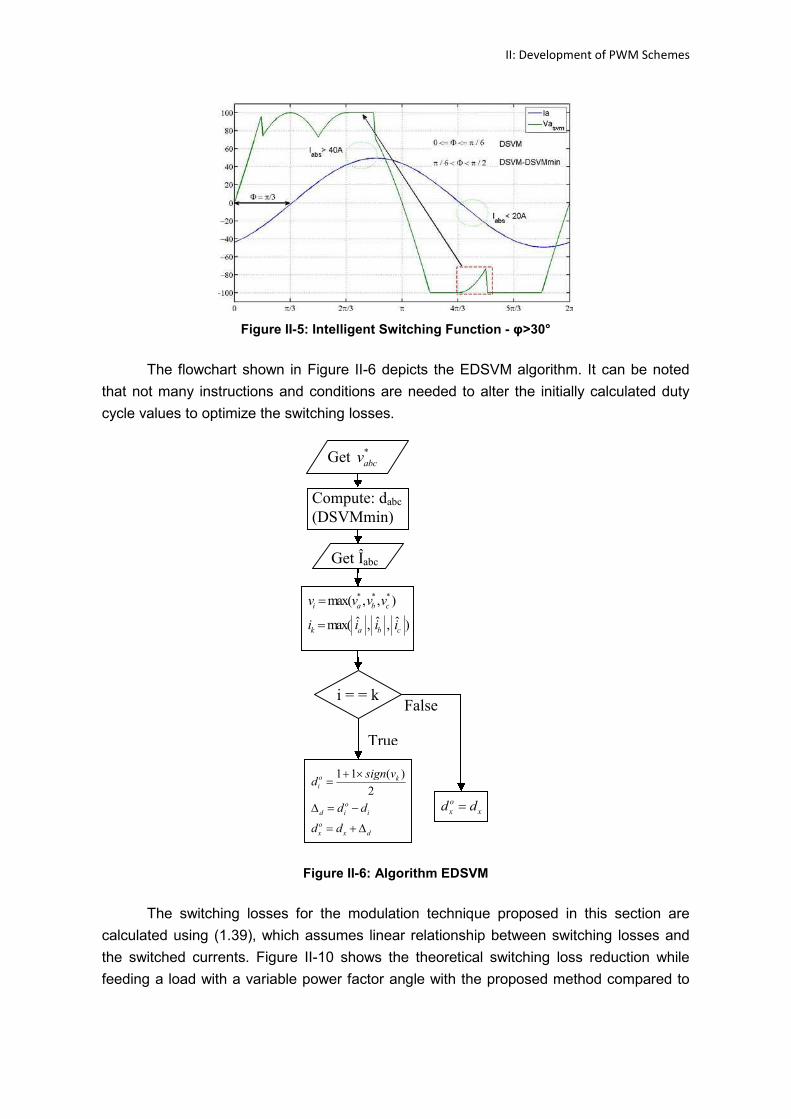
II: Development of PWM Schemes
Figure II-5: Intelligent Switching Function - φ>30°
The flowchart shown in Figure II-6 depicts the EDSVM algorithm. It can be noted
that not many instructions and conditions are needed to alter the initially calculated duty
cycle values to optimize the switching losses.
Figure II-6: Algorithm EDSVM
The switching losses for the modulation technique proposed in this section are
calculated using (1.39), which assumes linear relationship between switching losses and
the switched currents. Figure II-10 shows the theoretical switching loss reduction while
feeding a load with a variable power factor angle with the proposed method compared to
Get *abcv
Compute: dabc(DSVMmin)
Get Îabc
i = = k
* * *max( , , )
ˆ ˆ ˆmax( , , )
i a b c
k a b c
v v v v
i i i i
1 1 ( )
2o ki
o
d i i
o
x x d
sign vd
d d
d d
o
x xd d
False
True
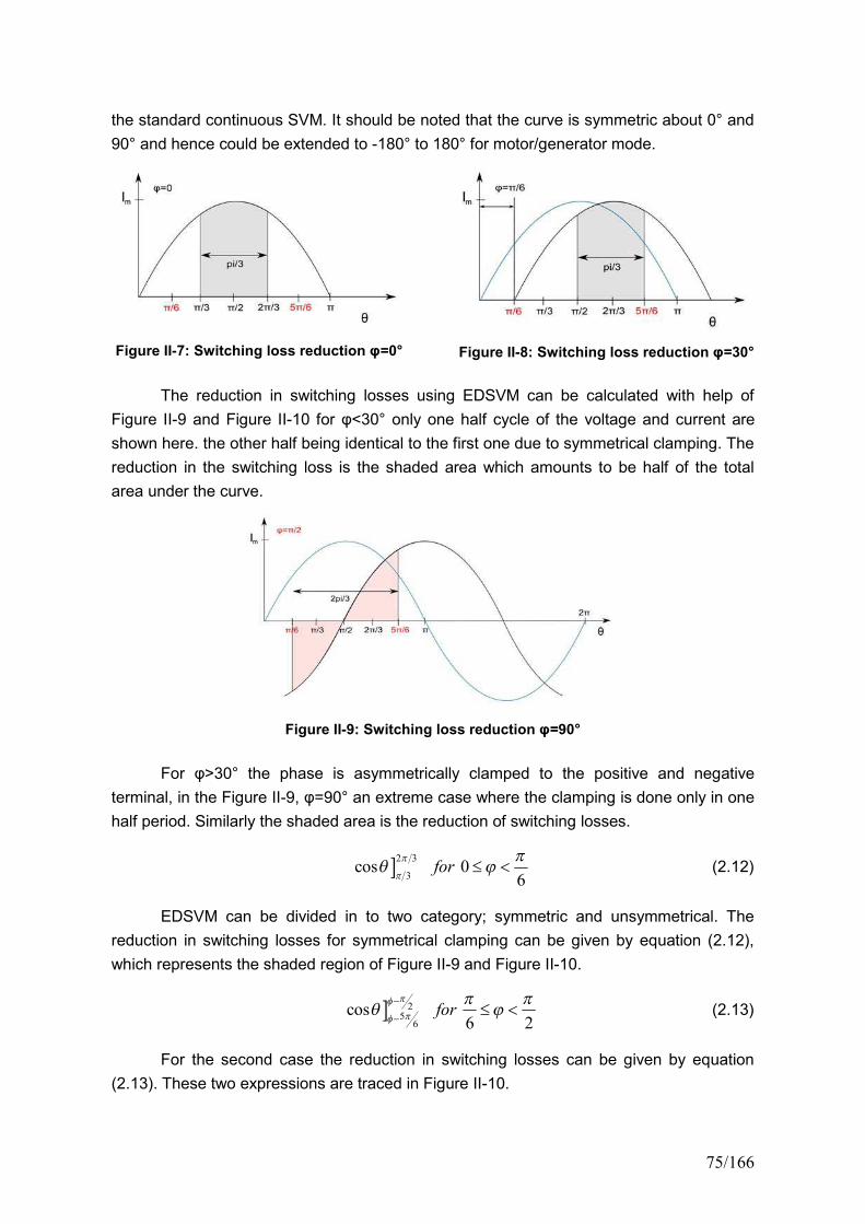
75/166
the standard continuous SVM. It should be noted that the curve is symmetric about 0° and
90° and hence could be extended to -180° to 180° for motor/generator mode.
Figure II-7: Switching loss reduction φ=0° Figure II-8: Switching loss reduction φ=30°
The reduction in switching losses using EDSVM can be calculated with help of
Figure II-9 and Figure II-10 for φ<30° only one half cycle of the voltage and current are shown here. the other half being identical to the first one due to symmetrical clamping. The
reduction in the switching loss is the shaded area which amounts to be half of the total
area under the curve.
Figure II-9: Switching loss reduction φ=90°
For φ>30° the phase is asymmetrically clamped to the positive and negative terminal, in the Figure II-9, φ=90° an extreme case where the clamping is done only in one half period. Similarly the shaded area is the reduction of switching losses.
2 3
3cos 0
6for
(2.12)
EDSVM can be divided in to two category; symmetric and unsymmetrical. The
reduction in switching losses for symmetrical clamping can be given by equation (2.12),
which represents the shaded region of Figure II-9 and Figure II-10.
256
cos6 2
for
(2.13)
For the second case the reduction in switching losses can be given by equation
(2.13). These two expressions are traced in Figure II-10.
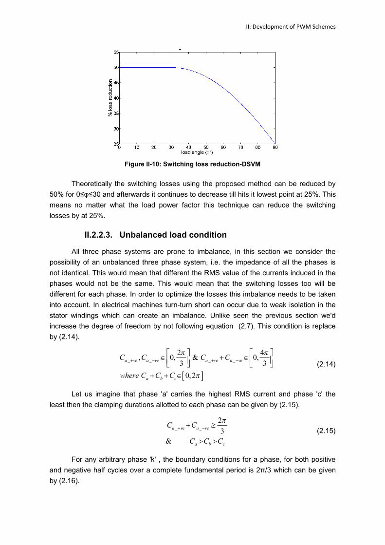
II: Development of PWM Schemes
Figure II-10: Switching loss reduction-DSVM
Theoretically the switching losses using the proposed method can be reduced by
50% for 0≤φ≤30 and afterwards it continues to decrease till hits it lowest point at 25%. This means no matter what the load power factor this technique can reduce the switching
losses by at 25%.
II.2.2.3. Unbalanced load condition
All three phase systems are prone to imbalance, in this section we consider the
possibility of an unbalanced three phase system, i.e. the impedance of all the phases is
not identical. This would mean that different the RMS value of the currents induced in the
phases would not be the same. This would mean that the switching losses too will be
different for each phase. In order to optimize the losses this imbalance needs to be taken
into account. In electrical machines turn-turn short can occur due to weak isolation in the
stator windings which can create an imbalance. Unlike seen the previous section we'd
increase the degree of freedom by not following equation (2.7). This condition is replace
by (2.14).
_ _ _ _
2 4, 0, & 0,
3 3
0,2
a ve a ve a ve a ve
a b c
C C C C
where C C C
(2.14)
Let us imagine that phase 'a' carries the highest RMS current and phase 'c' the
least then the clamping durations allotted to each phase can be given by (2.15).
_ _
2
3&
a ve a ve
a b c
C C
C C C
(2.15)
For any arbitrary phase 'k' , the boundary conditions for a phase, for both positive
and negative half cycles over a complete fundamental period is 2π/3 which can be given by (2.16).
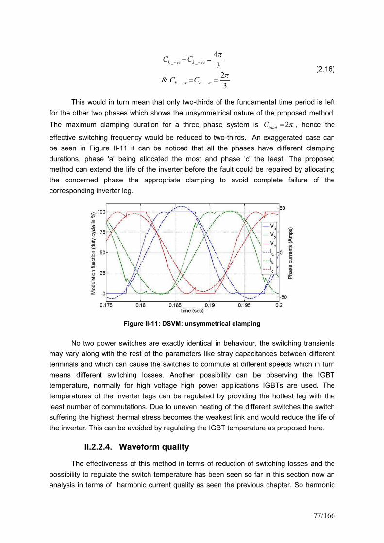
77/166
_ _
_ _
4
32
&3
k ve k ve
k ve k ve
C C
C C
(2.16)
This would in turn mean that only two-thirds of the fundamental time period is left
for the other two phases which shows the unsymmetrical nature of the proposed method.
The maximum clamping duration for a three phase system is 2totalC , hence the
effective switching frequency would be reduced to two-thirds. An exaggerated case can
be seen in Figure II-11 it can be noticed that all the phases have different clamping
durations, phase 'a' being allocated the most and phase 'c' the least. The proposed
method can extend the life of the inverter before the fault could be repaired by allocating
the concerned phase the appropriate clamping to avoid complete failure of the
corresponding inverter leg.
Figure II-11: DSVM: unsymmetrical clamping
No two power switches are exactly identical in behaviour, the switching transients
may vary along with the rest of the parameters like stray capacitances between different
terminals and which can cause the switches to commute at different speeds which in turn
means different switching losses. Another possibility can be observing the IGBT
temperature, normally for high voltage high power applications IGBTs are used. The
temperatures of the inverter legs can be regulated by providing the hottest leg with the
least number of commutations. Due to uneven heating of the different switches the switch
suffering the highest thermal stress becomes the weakest link and would reduce the life of
the inverter. This can be avoided by regulating the IGBT temperature as proposed here.
II.2.2.4. Waveform quality
The effectiveness of this method in terms of reduction of switching losses and the
possibility to regulate the switch temperature has been seen so far in this section now an
analysis in terms of harmonic current quality as seen the previous chapter. So harmonic
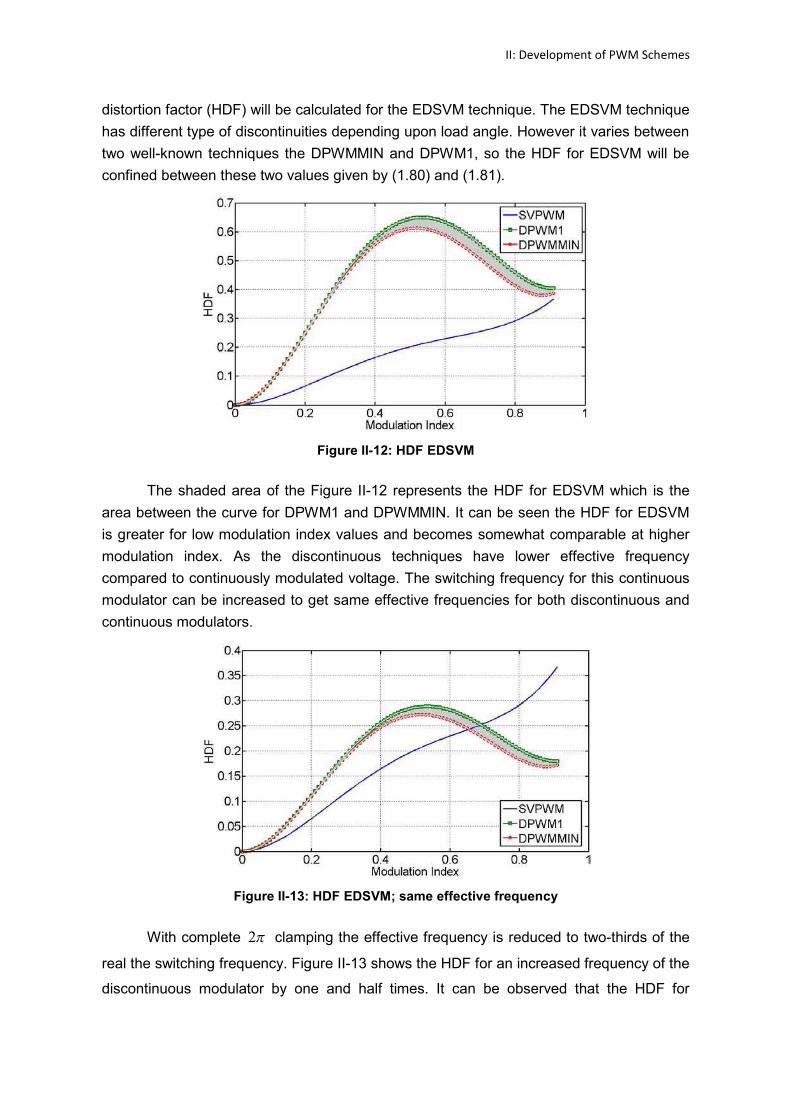
II: Development of PWM Schemes
distortion factor (HDF) will be calculated for the EDSVM technique. The EDSVM technique
has different type of discontinuities depending upon load angle. However it varies between
two well-known techniques the DPWMMIN and DPWM1, so the HDF for EDSVM will be
confined between these two values given by (1.80) and (1.81).
Figure II-12: HDF EDSVM
The shaded area of the Figure II-12 represents the HDF for EDSVM which is the
area between the curve for DPWM1 and DPWMMIN. It can be seen the HDF for EDSVM
is greater for low modulation index values and becomes somewhat comparable at higher
modulation index. As the discontinuous techniques have lower effective frequency
compared to continuously modulated voltage. The switching frequency for this continuous
modulator can be increased to get same effective frequencies for both discontinuous and
continuous modulators.
Figure II-13: HDF EDSVM; same effective frequency
With complete 2 clamping the effective frequency is reduced to two-thirds of the
real the switching frequency. Figure II-13 shows the HDF for an increased frequency of the
discontinuous modulator by one and half times. It can be observed that the HDF for
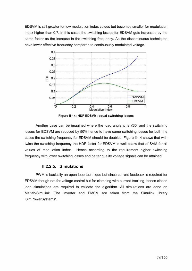
79/166
EDSVM is still greater for low modulation index values but becomes smaller for modulation
index higher than 0.7. In this cases the switching losses for EDSVM gets increased by the
same factor as the increase in the switching frequency. As the discontinuous techniques
have lower effective frequency compared to continuously modulated voltage.
Figure II-14: HDF EDSVM; equal switching losses
Another case can be imagined where the load angle φ is ≤30, and the switching
losses for EDSVM are reduced by 50% hence to have same switching losses for both the
cases the switching frequency for EDSVM should be doubled. Figure II-14 shows that with
twice the switching frequency the HDF factor for EDSVM is well below that of SVM for all
values of modulation index. Hence according to the requirement higher switching
frequency with lower switching losses and better quality voltage signals can be attained.
II.2.2.5. Simulations
PWM is basically an open loop technique but since current feedback is required for
EDSVM though not for voltage control but for clamping with current tracking, hence closed
loop simulations are required to validate the algorithm. All simulations are done on
Matlab/Simulink. The inverter and PMSM are taken from the Simulink library
'SimPowerSystems'.
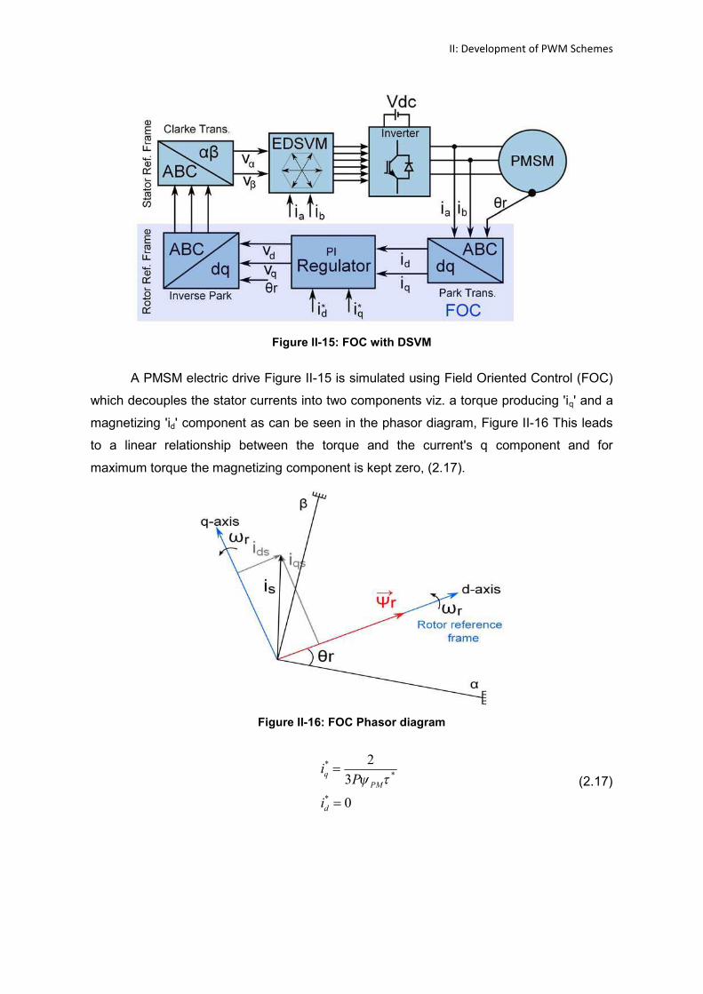
II: Development of PWM Schemes
Figure II-15: FOC with DSVM
A PMSM electric drive Figure II-15 is simulated using Field Oriented Control (FOC)
which decouples the stator currents into two components viz. a torque producing 'iq' and a
magnetizing 'id' component as can be seen in the phasor diagram, Figure II-16 This leads
to a linear relationship between the torque and the current's q component and for
maximum torque the magnetizing component is kept zero, (2.17).
Figure II-16: FOC Phasor diagram
**
*
2
3
0
q
PM
d
iP
i
(2.17)
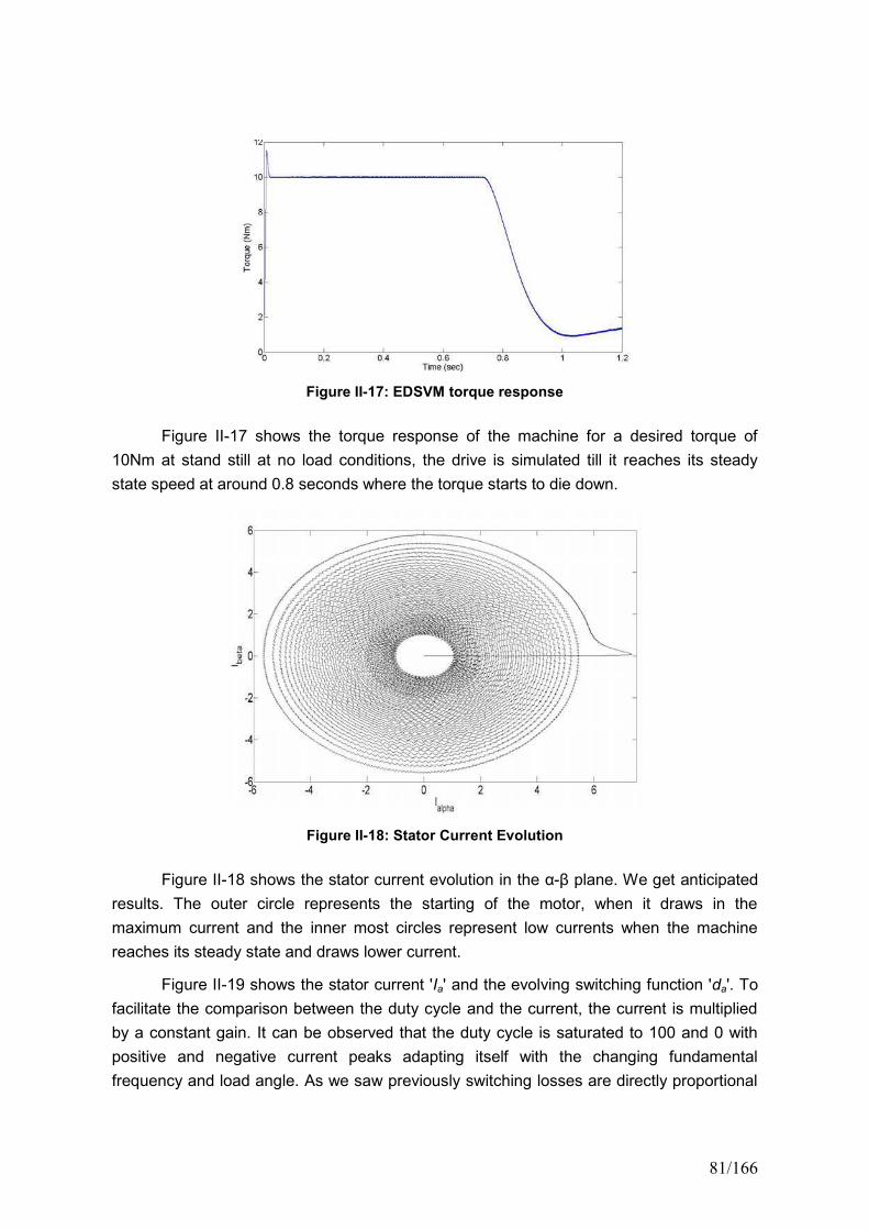
81/166
Figure II-17: EDSVM torque response
Figure II-17 shows the torque response of the machine for a desired torque of
10Nm at stand still at no load conditions, the drive is simulated till it reaches its steady
state speed at around 0.8 seconds where the torque starts to die down.
Figure II-18: Stator Current Evolution
Figure II-18 shows the stator current evolution in the α-β plane. We get anticipated results. The outer circle represents the starting of the motor, when it draws in the
maximum current and the inner most circles represent low currents when the machine
reaches its steady state and draws lower current.
Figure II-19 shows the stator current 'Ia' and the evolving switching function 'da'. To
facilitate the comparison between the duty cycle and the current, the current is multiplied
by a constant gain. It can be observed that the duty cycle is saturated to 100 and 0 with
positive and negative current peaks adapting itself with the changing fundamental
frequency and load angle. As we saw previously switching losses are directly proportional
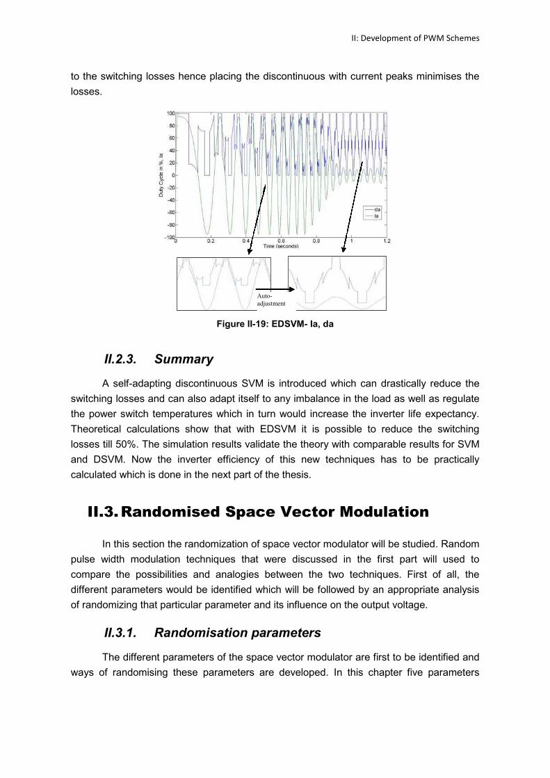
II: Development of PWM Schemes
to the switching losses hence placing the discontinuous with current peaks minimises the
losses.
Figure II-19: EDSVM- Ia, da
II.2.3. Summary
A self-adapting discontinuous SVM is introduced which can drastically reduce the
switching losses and can also adapt itself to any imbalance in the load as well as regulate
the power switch temperatures which in turn would increase the inverter life expectancy.
Theoretical calculations show that with EDSVM it is possible to reduce the switching
losses till 50%. The simulation results validate the theory with comparable results for SVM
and DSVM. Now the inverter efficiency of this new techniques has to be practically
calculated which is done in the next part of the thesis.
II.3.Randomised Space Vector Modulation
In this section the randomization of space vector modulator will be studied. Random
pulse width modulation techniques that were discussed in the first part will used to
compare the possibilities and analogies between the two techniques. First of all, the
different parameters would be identified which will be followed by an appropriate analysis
of randomizing that particular parameter and its influence on the output voltage.
II.3.1. Randomisation parameters
The different parameters of the space vector modulator are first to be identified and
ways of randomising these parameters are developed. In this chapter five parameters
Auto-adjustment
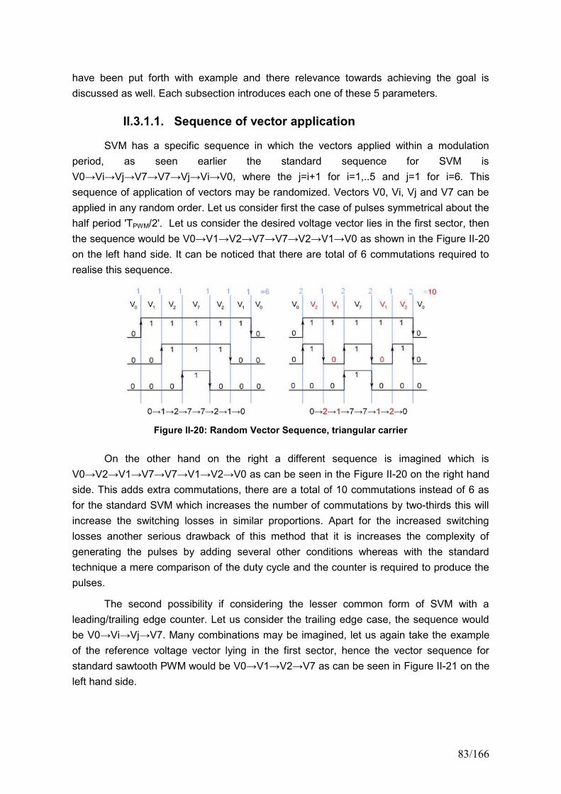
83/166
have been put forth with example and there relevance towards achieving the goal is
discussed as well. Each subsection introduces each one of these 5 parameters.
II.3.1.1. Sequence of vector application
SVM has a specific sequence in which the vectors applied within a modulation
period, as seen earlier the standard sequence for SVM is
V0→Vi→Vj→V7→V7→Vj→Vi→V0, where the j=i+1 for i=1,..5 and j=1 for i=6. This sequence of application of vectors may be randomized. Vectors V0, Vi, Vj and V7 can be
applied in any random order. Let us consider first the case of pulses symmetrical about the
half period 'TPWM/2'. Let us consider the desired voltage vector lies in the first sector, then
the sequence would be V0→V1→V2→V7→V7→V2→V1→V0 as shown in the Figure II-20 on the left hand side. It can be noticed that there are total of 6 commutations required to
realise this sequence.
Figure II-20: Random Vector Sequence, triangular carrier
On the other hand on the right a different sequence is imagined which is
V0→V2→V1→V7→V7→V1→V2→V0 as can be seen in the Figure II-20 on the right hand side. This adds extra commutations, there are a total of 10 commutations instead of 6 as
for the standard SVM which increases the number of commutations by two-thirds this will
increase the switching losses in similar proportions. Apart for the increased switching
losses another serious drawback of this method that it is increases the complexity of
generating the pulses by adding several other conditions whereas with the standard
technique a mere comparison of the duty cycle and the counter is required to produce the
pulses.
The second possibility if considering the lesser common form of SVM with a
leading/trailing edge counter. Let us consider the trailing edge case, the sequence would
be V0→Vi→Vj→V7. Many combinations may be imagined, let us again take the example of the reference voltage vector lying in the first sector, hence the vector sequence for
standard sawtooth PWM would be V0→V1→V2→V7 as can be seen in Figure II-21 on the left hand side.
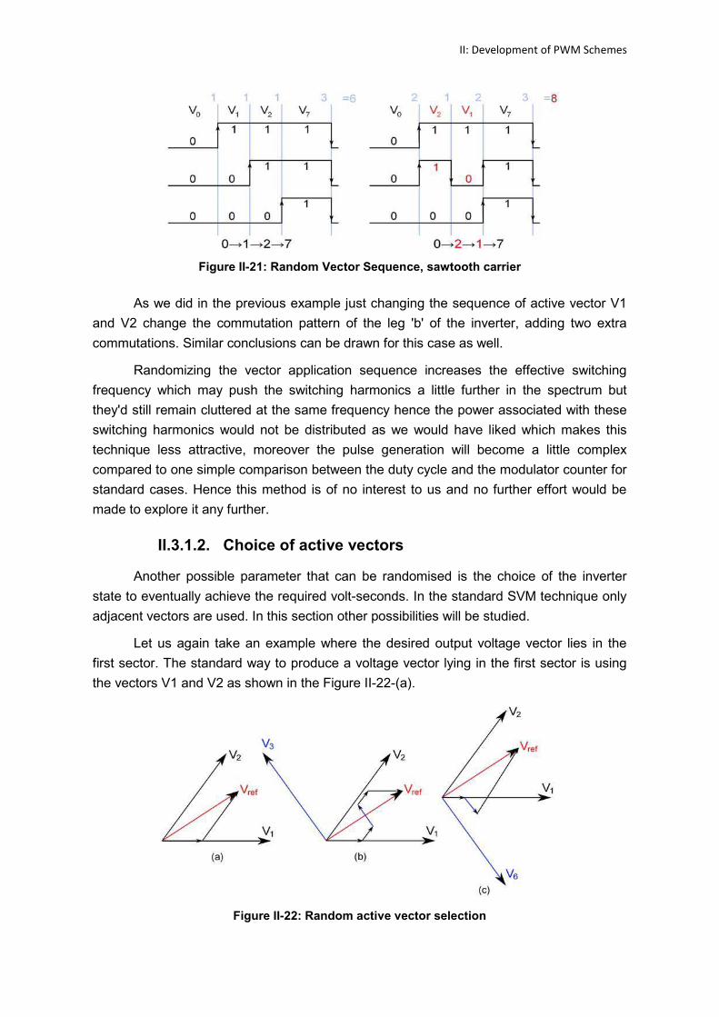
II: Development of PWM Schemes
Figure II-21: Random Vector Sequence, sawtooth carrier
As we did in the previous example just changing the sequence of active vector V1
and V2 change the commutation pattern of the leg 'b' of the inverter, adding two extra
commutations. Similar conclusions can be drawn for this case as well.
Randomizing the vector application sequence increases the effective switching
frequency which may push the switching harmonics a little further in the spectrum but
they'd still remain cluttered at the same frequency hence the power associated with these
switching harmonics would not be distributed as we would have liked which makes this
technique less attractive, moreover the pulse generation will become a little complex
compared to one simple comparison between the duty cycle and the modulator counter for
standard cases. Hence this method is of no interest to us and no further effort would be
made to explore it any further.
II.3.1.2. Choice of active vectors
Another possible parameter that can be randomised is the choice of the inverter
state to eventually achieve the required volt-seconds. In the standard SVM technique only
adjacent vectors are used. In this section other possibilities will be studied.
Let us again take an example where the desired output voltage vector lies in the
first sector. The standard way to produce a voltage vector lying in the first sector is using
the vectors V1 and V2 as shown in the Figure II-22-(a).
Figure II-22: Random active vector selection
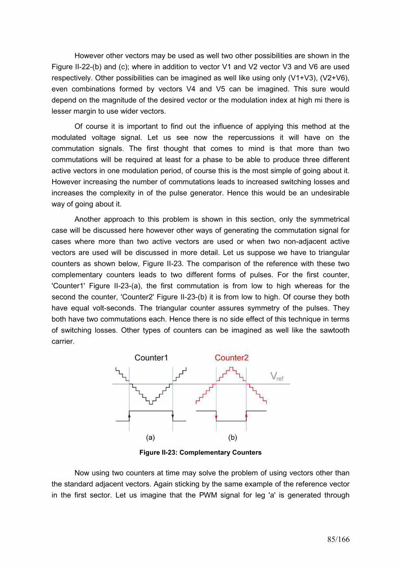
85/166
However other vectors may be used as well two other possibilities are shown in the
Figure II-22-(b) and (c); where in addition to vector V1 and V2 vector V3 and V6 are used
respectively. Other possibilities can be imagined as well like using only (V1+V3), (V2+V6),
even combinations formed by vectors V4 and V5 can be imagined. This sure would
depend on the magnitude of the desired vector or the modulation index at high mi there is
lesser margin to use wider vectors.
Of course it is important to find out the influence of applying this method at the
modulated voltage signal. Let us see now the repercussions it will have on the
commutation signals. The first thought that comes to mind is that more than two
commutations will be required at least for a phase to be able to produce three different
active vectors in one modulation period, of course this is the most simple of going about it.
However increasing the number of commutations leads to increased switching losses and
increases the complexity in of the pulse generator. Hence this would be an undesirable
way of going about it.
Another approach to this problem is shown in this section, only the symmetrical
case will be discussed here however other ways of generating the commutation signal for
cases where more than two active vectors are used or when two non-adjacent active
vectors are used will be discussed in more detail. Let us suppose we have to triangular
counters as shown below, Figure II-23. The comparison of the reference with these two
complementary counters leads to two different forms of pulses. For the first counter,
'Counter1' Figure II-23-(a), the first commutation is from low to high whereas for the
second the counter, 'Counter2' Figure II-23-(b) it is from low to high. Of course they both
have equal volt-seconds. The triangular counter assures symmetry of the pulses. They
both have two commutations each. Hence there is no side effect of this technique in terms
of switching losses. Other types of counters can be imagined as well like the sawtooth
carrier.
Figure II-23: Complementary Counters
Now using two counters at time may solve the problem of using vectors other than
the standard adjacent vectors. Again sticking by the same example of the reference vector
in the first sector. Let us imagine that the PWM signal for leg 'a' is generated through
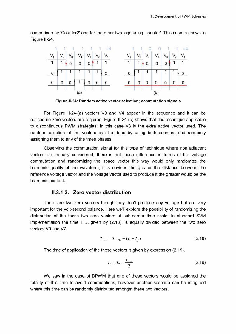
II: Development of PWM Schemes
comparison by 'Counter2' and for the other two legs using 'counter'. This case in shown in
Figure II-24.
Figure II-24: Random active vector selection; commutation signals
For Figure II-24-(a) vectors V3 and V4 appear in the sequence and it can be
noticed no zero vectors are required. Figure II-24-(b) shows that this technique applicable
to discontinuous PWM strategies. In this case V3 is the extra active vector used. The
random selection of the vectors can be done by using both counters and randomly
assigning them to any of the three phases.
Observing the commutation signal for this type of technique where non adjacent
vectors are equally considered, there is not much difference in terms of the voltage
commutation and randomizing the space vector this way would only randomize the
harmonic quality of the waveform, it is obvious the greater the distance between the
reference voltage vector and the voltage vector used to produce it the greater would be the
harmonic content.
II.3.1.3. Zero vector distribution
There are two zero vectors though they don't produce any voltage but are very
important for the volt-second balance. Here we'll explore the possibility of randomizing the
distribution of the these two zero vectors at sub-carrier time scale. In standard SVM
implementation the time Tzero given by (2.18), is equally divided between the two zero
vectors V0 and V7.
( )zero PWM i jT T T T (2.18)
The time of application of the these vectors is given by expression (2.19).
0 7 2zeroT
T T (2.19)
We saw in the case of DPWM that one of these vectors would be assigned the
totality of this time to avoid commutations, however another scenario can be imagined
where this time can be randomly distributed amongst these two vectors.
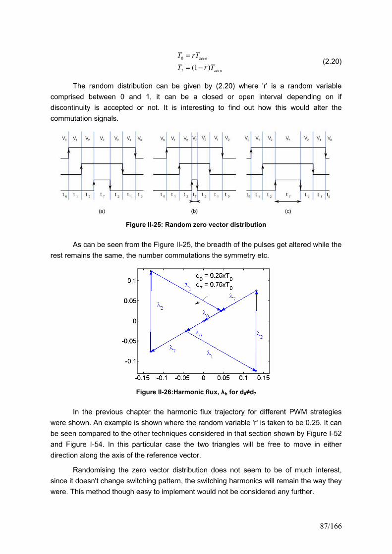
87/166
0
7 (1 )zero
zero
T rT
T r T
(2.20)
The random distribution can be given by (2.20) where 'r' is a random variable
comprised between 0 and 1, it can be a closed or open interval depending on if
discontinuity is accepted or not. It is interesting to find out how this would alter the
commutation signals.
Figure II-25: Random zero vector distribution
As can be seen from the Figure II-25, the breadth of the pulses get altered while the
rest remains the same, the number commutations the symmetry etc.
Figure II-26:Harmonic flux, λh for d0≠d7
In the previous chapter the harmonic flux trajectory for different PWM strategies
were shown. An example is shown where the random variable 'r' is taken to be 0.25. It can
be seen compared to the other techniques considered in that section shown by Figure I-52
and Figure I-54. In this particular case the two triangles will be free to move in either
direction along the axis of the reference vector.
Randomising the zero vector distribution does not seem to be of much interest,
since it doesn't change switching pattern, the switching harmonics will remain the way they
were. This method though easy to implement would not be considered any further.
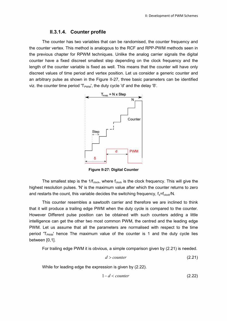
II: Development of PWM Schemes
II.3.1.4. Counter profile
The counter has two variables that can be randomised, the counter frequency and
the counter vertex. This method is analogous to the RCF and RPP-PWM methods seen in
the previous chapter for RPWM techniques. Unlike the analog carrier signals the digital
counter have a fixed discreet smallest step depending on the clock frequency and the
length of the counter variable is fixed as well. This means that the counter will have only
discreet values of time period and vertex position. Let us consider a generic counter and
an arbitrary pulse as shown in the Figure II-27, three basic parameters can be identified
viz. the counter time period 'TPWM', the duty cycle 'd' and the delay 'δ'.
Figure II-27: Digital Counter
The smallest step is the 1/fclock, where fclock is the clock frequency. This will give the
highest resolution pulses. 'N' is the maximum value after which the counter returns to zero
and restarts the count, this variable decides the switching frequency, fs=fclock/N.
This counter resembles a sawtooth carrier and therefore we are inclined to think
that it will produce a trailing edge PWM when the duty cycle is compared to the counter.
However Different pulse position can be obtained with such counters adding a little
intelligence can get the other two most common PWM, the centred and the leading edge
PWM. Let us assume that all the parameters are normalised with respect to the time
period 'TPWM' hence The maximum value of the counter is 1 and the duty cycle lies
between [0,1].
For trailing edge PWM it is obvious, a simple comparison given by (2.21) is needed.
d counter (2.21)
While for leading edge the expression is given by (2.22).
1 d counter (2.22)
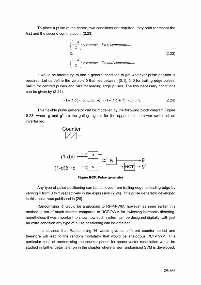
89/166
To place a pulse at the centre, two conditions are required, they both represent the
first and the second commutation, (2.23).
1,
2
&
1,
2
dcounter First commutation
dcounter Second commutation
(2.23)
It would be interesting to find a general condition to get whatever pulse position is
required. Let us define the variable δ that lies between [0,1]. δ=0 for trailing edge pulses, δ=0.5 for centred pulses and δ=1 for leading edge pulses. The two necessary conditions can be given by (2.24).
(1 ) & (1 )d counter d d counter (2.24)
This flexible pulse generator can be modelled by the following block diagram Figure
II-28, where g and g' are the gating signals for the upper and the lower switch of an
inverter leg.
Figure II-28: Pulse generator
Any type of pulse positioning can be achieved from trailing edge to leading edge by
varying δ from 0 to 1 respectively in the expression (2.24). This pulse generator developed in this thesis was published in [28].
Randomising 'δ' would be analogous to RPP-PWM, however as seen earlier this method is not of much interest compared to RCF-PWM for switching harmonic dithering,
nonetheless it was important to show how such system can be designed digitally, with just
an extra condition any type of pulse positioning can be obtained.
It is obvious that Randomising 'N' would give us different counter period and
therefore will lead to the random modulator that would be analogous RCF-PWM. This
particular case of randomising the counter period for space vector modulation would be
studied in further detail later on in the chapter where a new randomised SVM is developed.
II: Development of PWM Schemes
In this section we saw all the space vector modulator parameters that could be
randomised and there effect on the output voltage harmonics, before going any further with
the development of a randomised modulator we should think of how are we going to
provide this the required randomness to the system. The next section will give us some
insight into random numbers and their generation.
II.3.2. Random number generation
A random number source is a prerequisite for any RPWM technique. Normally
random number are generated by physical process for example analog electric circuits can
be used. A physical random number generator can be based on an essentially random
atomic or subatomic physical phenomenon whose unpredictability can be traced to the
laws of quantum mechanics. Hence such things cannot be programmed and need external
information from physical systems. For this reason algorithms are developed to be able to
produce a sequence which appears random with a suitable period before which it starts to
repeat itself, hence these are called Pseudorandom numbers. professor D. H. Lehmer
defined random numbers as:
A random sequence is a vague notion ... in which each term is unpredictable to the
uninitiated and whose digits pass a certain number of tests traditional with
statisticians ...
For most applications pseudorandom numbers generated by software may be
acceptable. A lot of research has been done on pseudorandom number generators. Just to
get an idea we'll see a couple of famous methods vastly used. The most common random
number generator is the multiplicative congruential algorithm also introduced by
Prof. Lehmer given by (2.25).
1 ( )modk kx ax c m (2.25)
Many of today's random number generators use this algorithm. Lehmer's
generators involve three integer parameters, a, c, and m, and an initial value, x0, called the
seed. The period of the sequence is m-1.
The Matlab function 'rand' till 1995 used this algorithm with the following values
given by (2.26) and recommended by [43] which make the arithmetic mod and
multiplication quicker.
5
31
7 ,
0,
2 1
a
c
m
(2.26)
With these parameters the sequence of the multiplicative congruential is 231-2
which is 2147483646 which is a huge period. To give an idea, a modulator with an
expected mean frequency of 20kHz can run for 4 days without repeating the same
frequencies.
91/166
However Matlab has switched to another algorithm which is based on the
Marsaglia-Zaman random number generator [45]. Unlike Lehmer's multiplicative
congruential algorithm Marsaglia-Zaman's doesn't involve any multiplications and
divisions. It is specifically designed to produce floating-point values. The results are not
just scaled integers. In place of a single seed, the new generator has 35 words of internal
memory or state. Thirty-two of these words form a cache of floating-point numbers, z,
between 0 and 1. The remaining three words contain an integer index i, which varies
between 0 and 31, a single random integer j, and a "borrow" flag b. This entire state vector
is built up a bit at a time during an initialization phase. Different values of j yield different
initial states. The generation of the ith floating-point number in the sequence involves a
"subtract-with-borrow" step, where one number in the cache is replaced with the difference
of two others, as expressed by (2.27).
20 5i i iz z z b (2.27)
The three indices, i, i+20, and i+5, are all interpreted mod 32 (by using just their last
five bits). The quantity b is left over from the previous step; it is either zero or a small
positive value. If the computed zi is positive, b is set to zero for the next step. But if the
computed zi is negative, it is made positive by adding 1 before it is saved and b is set to
2-53 for the next step. This method has a huge period of about 21430. However Matlab's
modified version of Marsaglia-Zaman would generate uniformly spaced 21492 random
numbers comprised between 0 and 1 before repeating itself.
We have used Matlab's modified version of Marsaglia-Zaman random number
generator algorithm throughout the work, for simulations as well as for experimental tests.
II.3.3. Random Space Vector Modulation
Random Space Vector Modulation (RSVM), a new solution is proposed to conserve
the advantages of SVM while adding those of the RCF-PWM. The proposed method is to
vary the switching frequency randomly and calculating the corresponding duty cycles. This
technique is analogous to RCF-PWM, here it is implemented digitally i.e. no carrier signals.
There are about half a dozen papers on RSVM; reading them thoroughly we find some
incoherence with the basic principles of SVM. [32] Proposes a 3-level inverter with RSVM
to reduce acoustic noise, however the generation of gate signals is done through
comparison of the reference signal by a triangular carrier signal, and this technique is
commonly known as SVPWM. [33] Proposes a random SVM technique, which is not really
random, only two switching frequencies are used with scalar control, however the pulse
generation remains ambiguous. Similarly there are other papers such as [34], [35] that
treat the problem in a similar way, which in our opinion requires to be treated further.
In the previous chapter it was seen that depending on how the inverter is fed
different common mode voltage is produced by different inverter state. For electric drives
fed through a battery whose negative terminal is grounded doesn't produce any common
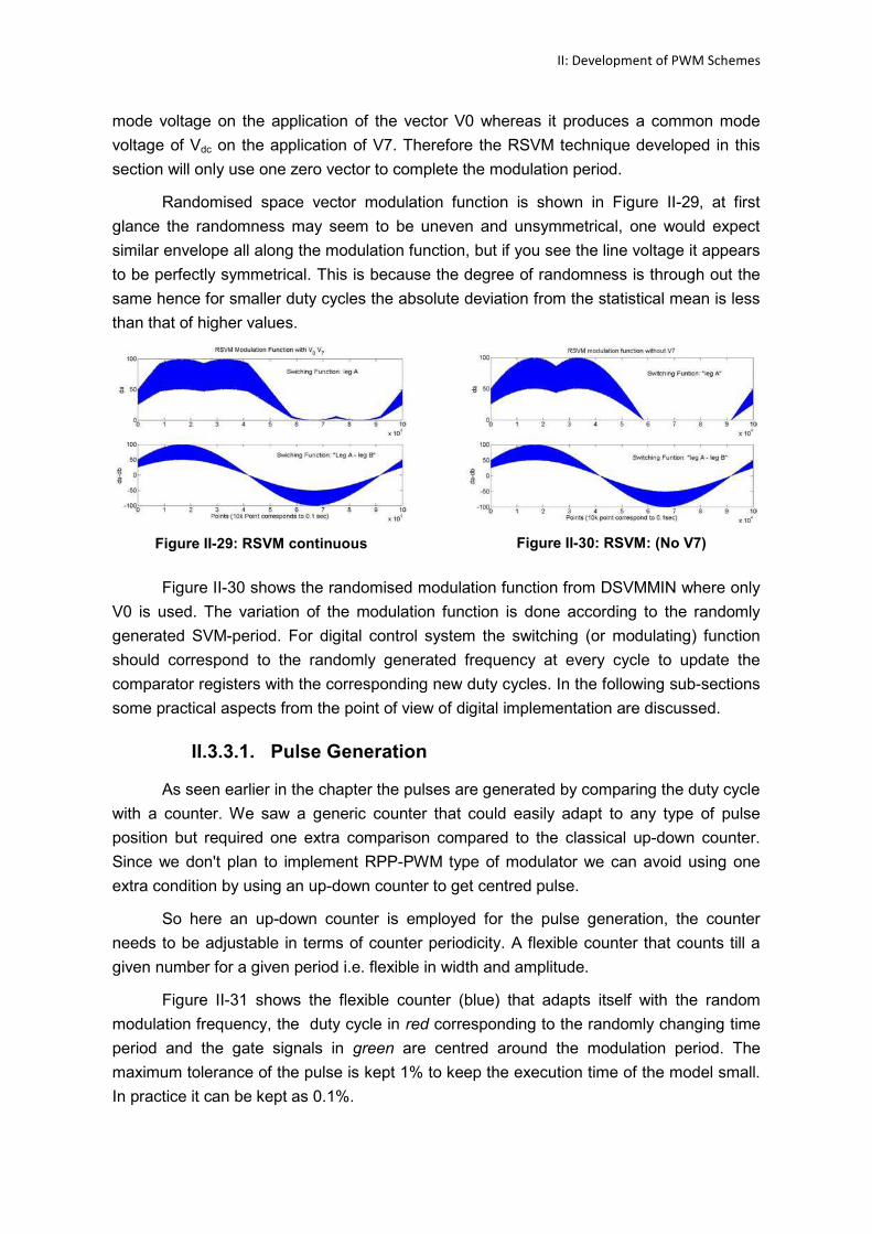
II: Development of PWM Schemes
mode voltage on the application of the vector V0 whereas it produces a common mode
voltage of Vdc on the application of V7. Therefore the RSVM technique developed in this
section will only use one zero vector to complete the modulation period.
Randomised space vector modulation function is shown in Figure II-29, at first
glance the randomness may seem to be uneven and unsymmetrical, one would expect
similar envelope all along the modulation function, but if you see the line voltage it appears
to be perfectly symmetrical. This is because the degree of randomness is through out the
same hence for smaller duty cycles the absolute deviation from the statistical mean is less
than that of higher values.
Figure II-29: RSVM continuous Figure II-30: RSVM: (No V7)
Figure II-30 shows the randomised modulation function from DSVMMIN where only
V0 is used. The variation of the modulation function is done according to the randomly
generated SVM-period. For digital control system the switching (or modulating) function
should correspond to the randomly generated frequency at every cycle to update the
comparator registers with the corresponding new duty cycles. In the following sub-sections
some practical aspects from the point of view of digital implementation are discussed.
II.3.3.1. Pulse Generation
As seen earlier in the chapter the pulses are generated by comparing the duty cycle
with a counter. We saw a generic counter that could easily adapt to any type of pulse
position but required one extra comparison compared to the classical up-down counter.
Since we don't plan to implement RPP-PWM type of modulator we can avoid using one
extra condition by using an up-down counter to get centred pulse.
So here an up-down counter is employed for the pulse generation, the counter
needs to be adjustable in terms of counter periodicity. A flexible counter that counts till a
given number for a given period i.e. flexible in width and amplitude.
Figure II-31 shows the flexible counter (blue) that adapts itself with the random
modulation frequency, the duty cycle in red corresponding to the randomly changing time
period and the gate signals in green are centred around the modulation period. The
maximum tolerance of the pulse is kept 1% to keep the execution time of the model small.
In practice it can be kept as 0.1%.
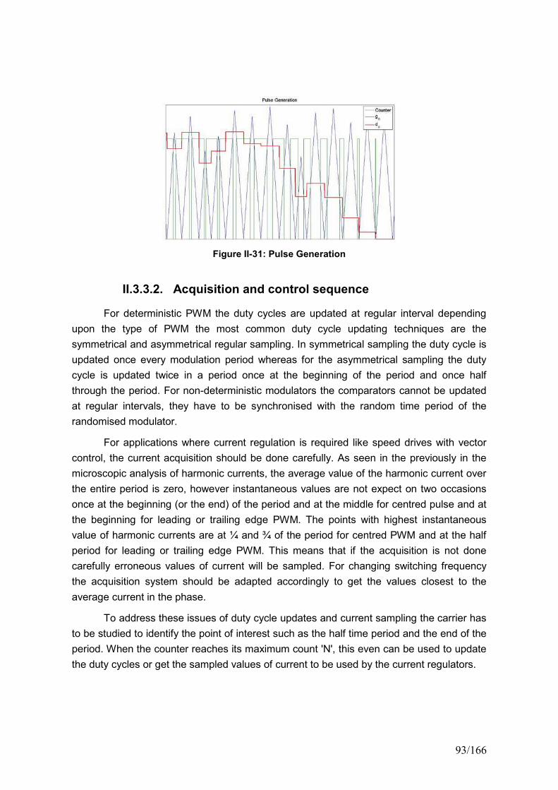
93/166
Figure II-31: Pulse Generation
II.3.3.2. Acquisition and control sequence
For deterministic PWM the duty cycles are updated at regular interval depending
upon the type of PWM the most common duty cycle updating techniques are the
symmetrical and asymmetrical regular sampling. In symmetrical sampling the duty cycle is
updated once every modulation period whereas for the asymmetrical sampling the duty
cycle is updated twice in a period once at the beginning of the period and once half
through the period. For non-deterministic modulators the comparators cannot be updated
at regular intervals, they have to be synchronised with the random time period of the
randomised modulator.
For applications where current regulation is required like speed drives with vector
control, the current acquisition should be done carefully. As seen in the previously in the
microscopic analysis of harmonic currents, the average value of the harmonic current over
the entire period is zero, however instantaneous values are not expect on two occasions
once at the beginning (or the end) of the period and at the middle for centred pulse and at
the beginning for leading or trailing edge PWM. The points with highest instantaneous
value of harmonic currents are at ¼ and ¾ of the period for centred PWM and at the half
period for leading or trailing edge PWM. This means that if the acquisition is not done
carefully erroneous values of current will be sampled. For changing switching frequency
the acquisition system should be adapted accordingly to get the values closest to the
average current in the phase.
To address these issues of duty cycle updates and current sampling the carrier has
to be studied to identify the point of interest such as the half time period and the end of the
period. When the counter reaches its maximum count 'N', this even can be used to update
the duty cycles or get the sampled values of current to be used by the current regulators.
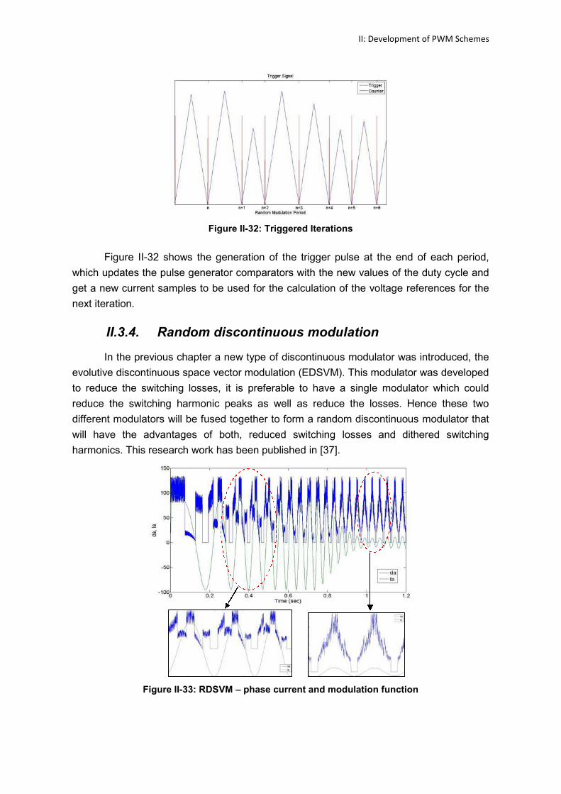
II: Development of PWM Schemes
Figure II-32: Triggered Iterations
Figure II-32 shows the generation of the trigger pulse at the end of each period,
which updates the pulse generator comparators with the new values of the duty cycle and
get a new current samples to be used for the calculation of the voltage references for the
next iteration.
II.3.4. Random discontinuous modulation
In the previous chapter a new type of discontinuous modulator was introduced, the
evolutive discontinuous space vector modulation (EDSVM). This modulator was developed
to reduce the switching losses, it is preferable to have a single modulator which could
reduce the switching harmonic peaks as well as reduce the losses. Hence these two
different modulators will be fused together to form a random discontinuous modulator that
will have the advantages of both, reduced switching losses and dithered switching
harmonics. This research work has been published in [37].
Figure II-33: RDSVM – phase current and modulation function
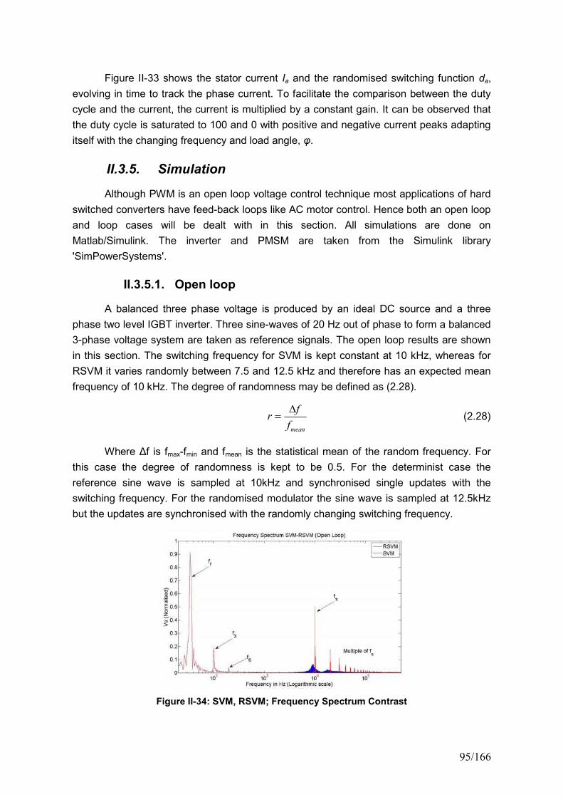
95/166
Figure II-33 shows the stator current Ia and the randomised switching function da,
evolving in time to track the phase current. To facilitate the comparison between the duty
cycle and the current, the current is multiplied by a constant gain. It can be observed that
the duty cycle is saturated to 100 and 0 with positive and negative current peaks adapting
itself with the changing frequency and load angle, φ.
II.3.5. Simulation
Although PWM is an open loop voltage control technique most applications of hard
switched converters have feed-back loops like AC motor control. Hence both an open loop
and loop cases will be dealt with in this section. All simulations are done on
Matlab/Simulink. The inverter and PMSM are taken from the Simulink library
'SimPowerSystems'.
II.3.5.1. Open loop
A balanced three phase voltage is produced by an ideal DC source and a three
phase two level IGBT inverter. Three sine-waves of 20 Hz out of phase to form a balanced
3-phase voltage system are taken as reference signals. The open loop results are shown
in this section. The switching frequency for SVM is kept constant at 10 kHz, whereas for
RSVM it varies randomly between 7.5 and 12.5 kHz and therefore has an expected mean
frequency of 10 kHz. The degree of randomness may be defined as (2.28).
mean
fr
f
(2.28)
Where Δf is fmax-fmin and fmean is the statistical mean of the random frequency. For
this case the degree of randomness is kept to be 0.5. For the determinist case the
reference sine wave is sampled at 10kHz and synchronised single updates with the
switching frequency. For the randomised modulator the sine wave is sampled at 12.5kHz
but the updates are synchronised with the randomly changing switching frequency.
Figure II-34: SVM, RSVM; Frequency Spectrum Contrast
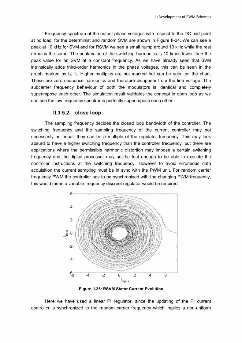
II: Development of PWM Schemes
Frequency spectrum of the output phase voltages with respect to the DC mid-point
at no load. for the determinist and random SVM are shown in Figure II-34. We can see a
peak at 10 kHz for SVM and for RSVM we see a small hump around 10 kHz while the rest
remains the same. The peak value of the switching harmonics is 10 times lower than the
peak value for an SVM at a constant frequency. As we have already seen that SVM
intrinsically adds third-order harmonics in the phase voltages, this can be seen in the
graph marked by f3, f6. Higher multiples are not marked but can be seen on the chart.
These are zero sequence harmonics and therefore disappear from the line voltage. The
subcarrier frequency behaviour of both the modulators is identical and completely
superimpose each other. The simulation result validates the concept in open loop as we
can see the low frequency spectrums perfectly superimpose each other.
II.3.5.2. close loop
The sampling frequency decides the closed loop bandwidth of the controller. The
switching frequency and the sampling frequency of the current controller may not
necessarily be equal, they can be a multiple of the regulator frequency. This may look
absurd to have a higher switching frequency than the controller frequency, but there are
applications where the permissible harmonic distortion may impose a certain switching
frequency and the digital processor may not be fast enough to be able to execute the
controller instructions at the switching frequency. However to avoid erroneous data
acquisition the current sampling must be in sync with the PWM unit. For random carrier
frequency PWM the controller has to be synchronised with the changing PWM frequency,
this would mean a variable frequency discreet regulator would be required.
Figure II-35: RSVM Stator Current Evolution
Here we have used a linear PI regulator, since the updating of the PI current
controller is synchronized to the random carrier frequency which implies a non-uniform
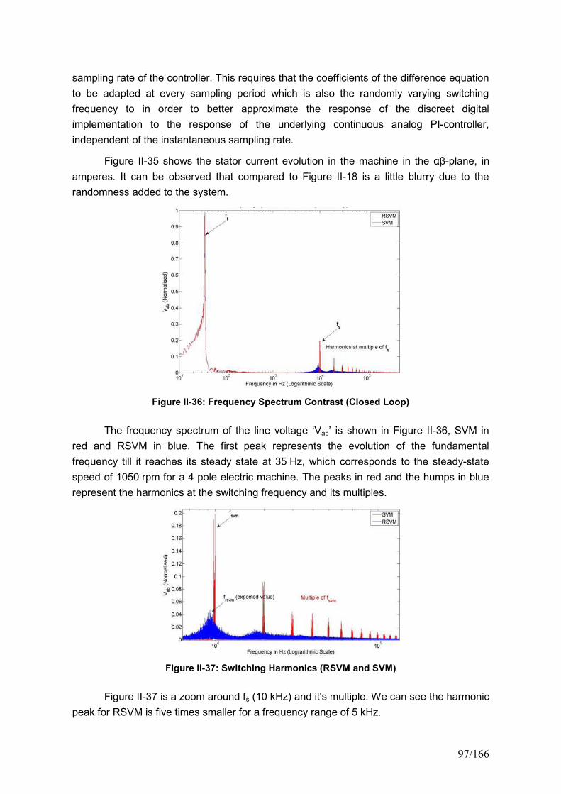
97/166
sampling rate of the controller. This requires that the coefficients of the difference equation
to be adapted at every sampling period which is also the randomly varying switching
frequency to in order to better approximate the response of the discreet digital
implementation to the response of the underlying continuous analog PI-controller,
independent of the instantaneous sampling rate.
Figure II-35 shows the stator current evolution in the machine in the αβ-plane, in amperes. It can be observed that compared to Figure II-18 is a little blurry due to the
randomness added to the system.
Figure II-36: Frequency Spectrum Contrast (Closed Loop)
The frequency spectrum of the line voltage ‘Vab’ is shown in Figure II-36, SVM in
red and RSVM in blue. The first peak represents the evolution of the fundamental
frequency till it reaches its steady state at 35 Hz, which corresponds to the steady-state
speed of 1050 rpm for a 4 pole electric machine. The peaks in red and the humps in blue
represent the harmonics at the switching frequency and its multiples.
Figure II-37: Switching Harmonics (RSVM and SVM)
Figure II-37 is a zoom around fs (10 kHz) and it's multiple. We can see the harmonic
peak for RSVM is five times smaller for a frequency range of 5 kHz.
II: Development of PWM Schemes
II.3.6. Summary
In this chapter we saw different types of randomisation possibilities for a space
vector modulator, their physical interpretation and their digital implementation. Amongst all
of the methods introduced only randomising carrier frequency was chosen because it was
the only modulator which alters the switching function to dither the switching harmonics
and alleviate the problem of acoustic noise annoyance in hard switched converters.
Different practical implementation aspects of the random carrier frequency
modulators such as system performance, acquisition of feedback signals and the design
considerations for the digital controller were discussed. Finally the validity of such
technique was established through simulations.
II.4.PWM Optimized embedded electric drives
The focus of this chapter is how a pulse width modulated drive be optimised in
terms of cost and volume but unlike in the previous chapters the focus would not be
entirely on the output voltage and the switching losses here even the DC current fed to the
inverter is studied at subcarrier period scale in correlation with the inverter discreet state.
Studying the inverter states and the DC input current, it is observed that the phase
currents can be deduced and the DC link current fluctuations may be reduced to which in
turn would mean a small stabilising capacitor at the inverter input. Different PWM
techniques would be introduced here, that can potentially reduce the cost and size of the
inverter drive by altering the PWM techniques a little.
II.4.1. Introduction
Embedded electric drives have certain design constraints which are the volume,
weight and robustness as they are more prone to varying working environment, harsh
temperatures, and possible mechanical shocks. Not to mention cost minimization is a very
important engineering aspect and is true for any application. In this section we'd develop
two modulation techniques which would reduce the design cost with decreased volume
and weight linked to the DC-link capacitor and a decrease in the number of current
sensors. Talk briefly about volume and the cost of stabilising capacitors add to the system.
similarly for the current sensors.
II.4.2. Phase current reconstruction
In this section we'll study the possibility of deducing the two phase currents
necessary for the feed-back control of PWM speed drives. Modulation strategy will be
developed allowing the possibility of removing the phase current sensors.
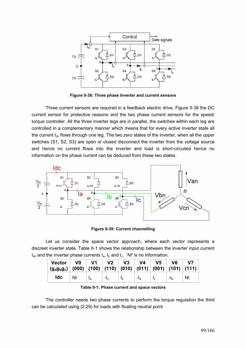
99/166
Figure II-38: Three phase Inverter and current sensors
Three current sensors are required in a feedback electric drive, Figure II-38 the DC
current sensor for protective reasons and the two phase current sensors for the speed/
torque controller. All the three inverter legs are in parallel, the switches within each leg are
controlled in a complementary manner which means that for every active inverter state all
the current Idc flows through one leg. The two zero states of the inverter, when all the upper
switches (S1, S2, S3) are open or closed disconnect the inverter from the voltage source
and hence no current flows into the inverter and load is short-circuited hence no
information on the phase current can be deduced from these two states.
Figure II-39: Current channelling
Let us consider the space vector approach, where each vector represents a
discreet inverter state. Table II-1 shows the relationship between the inverter input current
Idc and the inverter phase currents Ia, Ib and Ic. 'NI' is no information.
Vector(gagbgc)
V0(000)
V1(100)
V2(110)
V3(010)
V4(011)
V5(001)
V6(101)
V7(111)
Idc NI Ia -Ic Ib -Ia Ic -Ib NI
Table II-1: Phase current and space vectors
The controller needs two phase currents to perform the torque regulation the third
can be calculated using (2.29) for loads with floating neutral point.

II: Development of PWM Schemes
0a b cI I I (2.29)
One active vector gives information about only one phase current, hence for every
modulation period two active inverter states are required to successfully deduce the phase
currents and one zero vector for ground fault detection.
II.4.2.1. Limitations and Boundary conditions
Apart from the requirement of two active vectors per PWM period another limiting
factor is the absolute duration of vector application, the dead-time and the reverse
recovery time of the diode, this time should be sufficiently large for a stable analog to
digital conversion.
Figure II-40. Space vector representation
For small modulation index the inverter stays in the active states for a very short
duration and makes it impossible to get a stable current acquisition, hence for weak
modulation index standard modulation techniques won't work and to increase the
application time of active vectors non-adjacent vectors can be used. There are six limiting
cases where only one active vector or one inverter state is needed to produce the desired
average output voltage, the condition is given by (2.30) which essentially define the active
vector axis.
0 3ref ref ref
v OR v v (2.30)
In the vicinity of these axis represented by the shaded area of the Figure II-40
represents the regions where the length of one of the active vector or the inverter active
state duration is not long enough to extract the complete phase current information from
the Idc measurement.

101/166
II.4.2.2. State of the art
A number of papers have been written to overcome these problems. [48] does a
review of the papers published on phase current reconstruction from the inverter input
current. The common techniques used are adding measurement vectors [46] where a set
of three active vectors V1, V3 and V5 are applied as shown in Figure II-41, each with a
duration long enough for accurate current measurement these vectors have zero average
value hence don't add to the average to desired voltage. The advantage of this method is
that all the three phase currents are reconstructed separately whereas the drawbacks are
high HDF and switching losses owing to the 6 extra commutations.
Figure II-41: Measurement vectors, [46]
Another way is to add an extra active vector in the by displacing the pulse in the
modulation period [48].
Figure II-42: Pulse displacement, [48]
Figure II-42 shows a case where db=dc and only the current in phase can be
detected whereas shifting the two pulses all the three phase currents can be reconstructed
from the inverter input current. This can equally be used where the duty cycles are nearly
equal.
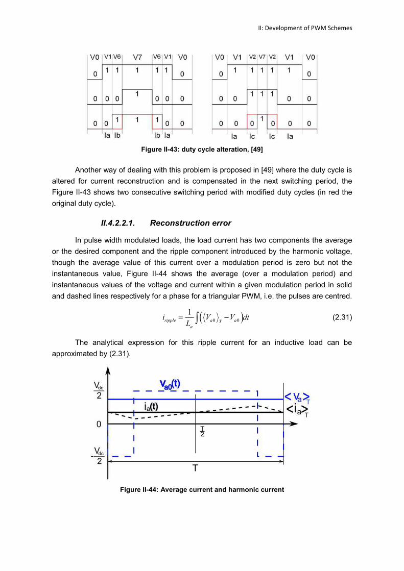
II: Development of PWM Schemes
Figure II-43: duty cycle alteration, [49]
Another way of dealing with this problem is proposed in [49] where the duty cycle is
altered for current reconstruction and is compensated in the next switching period, the
Figure II-43 shows two consecutive switching period with modified duty cycles (in red the
original duty cycle).
II.4.2.2.1. Reconstruction error
In pulse width modulated loads, the load current has two components the average
or the desired component and the ripple component introduced by the harmonic voltage,
though the average value of this current over a modulation period is zero but not the
instantaneous value, Figure II-44 shows the average (over a modulation period) and
instantaneous values of the voltage and current within a given modulation period in solid
and dashed lines respectively for a phase for a triangular PWM, i.e. the pulses are centred.
0 0
1ripple a aT
a
i V V dtL
(2.31)
The analytical expression for this ripple current for an inductive load can be
approximated by (2.31).
Figure II-44: Average current and harmonic current

103/166
For current controlled pulse width modulated loads, the current regulators should be
fed the average value. From the Figure II-44 it can be observed that the ripple current is
zero on three occasions viz. at the beginning of the period, at half-period and at the end of
the period. The current acquisition should be done in a way to get the ripple free current
samples hence the current sampling has to be synchronised with the PWM.
However for phase current reconstruction from the DC link current sensing the
phase currents have to be synchronised with the inverter state and hence the values have
to be sampled somewhere within the switching period.
Figure II-45: Current reconstruction error elimination
Figure II-45 shows an example of current sampling to remove the ripple component
from the current sensed somewhere between the period. The dotted circles show the
sampling instances, the DC link current is sampled twice for each phase. (2.32) and (2.33)
should be used to get the desired average values of the phase currents.
'1 2( ) ( )
2dc dc
a T
i t i ti
(2.32)
'2 1( ) ( )
2dc dc
c T
i t i ti
(2.33)
This technique requires the pulses to be symmetrical about the half-period and that
the reference voltage vector to be in the comfortable zone to be able to get a suitably long
durations for accurate analog to digital conversions.
II.4.2.2.2. Fault Detection
An electric drive is vulnerable to different types of faults that can be destructive to
the inverter and the load if not detected and isolated quickly. So in general an electric drive
should be protected against:
Ground faults
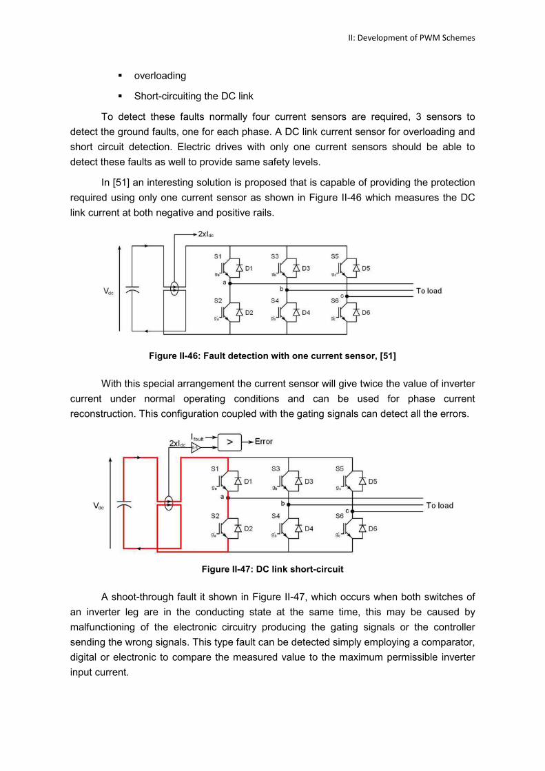
II: Development of PWM Schemes
overloading
Short-circuiting the DC link
To detect these faults normally four current sensors are required, 3 sensors to
detect the ground faults, one for each phase. A DC link current sensor for overloading and
short circuit detection. Electric drives with only one current sensors should be able to
detect these faults as well to provide same safety levels.
In [51] an interesting solution is proposed that is capable of providing the protection
required using only one current sensor as shown in Figure II-46 which measures the DC
link current at both negative and positive rails.
Figure II-46: Fault detection with one current sensor, [51]
With this special arrangement the current sensor will give twice the value of inverter
current under normal operating conditions and can be used for phase current
reconstruction. This configuration coupled with the gating signals can detect all the errors.
Figure II-47: DC link short-circuit
A shoot-through fault it shown in Figure II-47, which occurs when both switches of
an inverter leg are in the conducting state at the same time, this may be caused by
malfunctioning of the electronic circuitry producing the gating signals or the controller
sending the wrong signals. This type fault can be detected simply employing a comparator,
digital or electronic to compare the measured value to the maximum permissible inverter
input current.
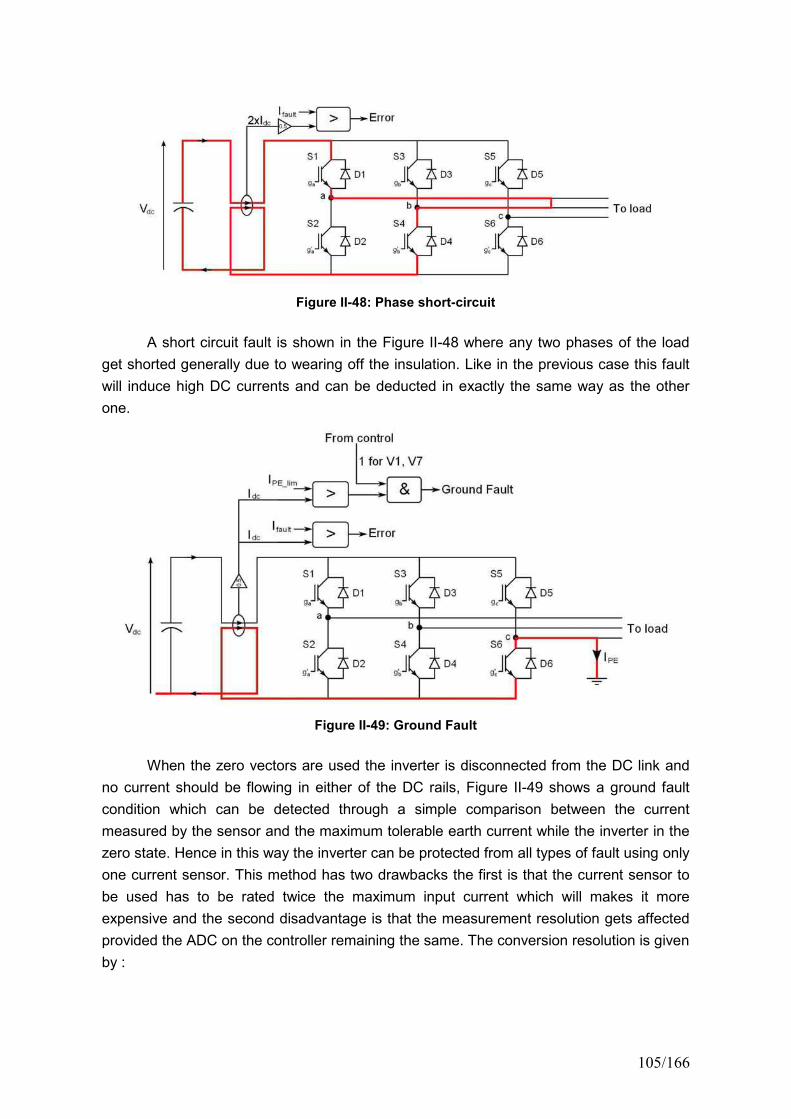
105/166
Figure II-48: Phase short-circuit
A short circuit fault is shown in the Figure II-48 where any two phases of the load
get shorted generally due to wearing off the insulation. Like in the previous case this fault
will induce high DC currents and can be deducted in exactly the same way as the other
one.
Figure II-49: Ground Fault
When the zero vectors are used the inverter is disconnected from the DC link and
no current should be flowing in either of the DC rails, Figure II-49 shows a ground fault
condition which can be detected through a simple comparison between the current
measured by the sensor and the maximum tolerable earth current while the inverter in the
zero state. Hence in this way the inverter can be protected from all types of fault using only
one current sensor. This method has two drawbacks the first is that the current sensor to
be used has to be rated twice the maximum input current which will makes it more
expensive and the second disadvantage is that the measurement resolution gets affected
provided the ADC on the controller remaining the same. The conversion resolution is given
by :
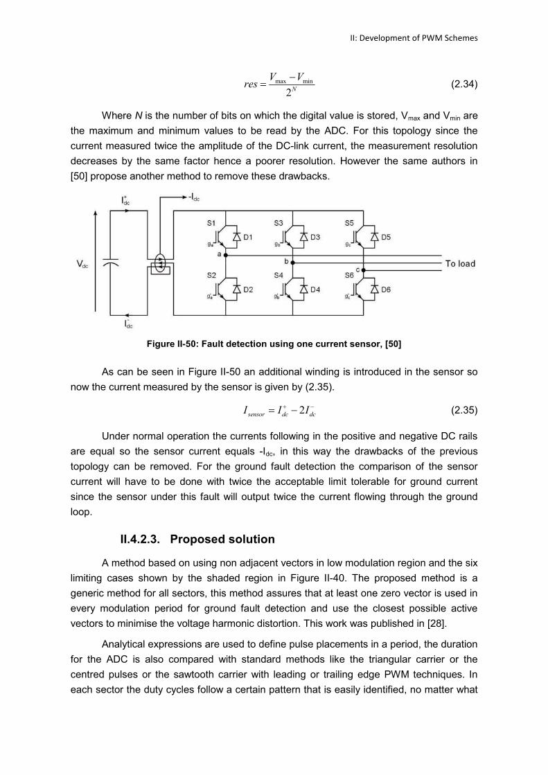
II: Development of PWM Schemes
max min
2NV V
res (2.34)
Where N is the number of bits on which the digital value is stored, Vmax and Vmin are
the maximum and minimum values to be read by the ADC. For this topology since the
current measured twice the amplitude of the DC-link current, the measurement resolution
decreases by the same factor hence a poorer resolution. However the same authors in
[50] propose another method to remove these drawbacks.
Figure II-50: Fault detection using one current sensor, [50]
As can be seen in Figure II-50 an additional winding is introduced in the sensor so
now the current measured by the sensor is given by (2.35).
2sensor dc dcI I I (2.35)
Under normal operation the currents following in the positive and negative DC rails
are equal so the sensor current equals -Idc, in this way the drawbacks of the previous
topology can be removed. For the ground fault detection the comparison of the sensor
current will have to be done with twice the acceptable limit tolerable for ground current
since the sensor under this fault will output twice the current flowing through the ground
loop.
II.4.2.3. Proposed solution
A method based on using non adjacent vectors in low modulation region and the six
limiting cases shown by the shaded region in Figure II-40. The proposed method is a
generic method for all sectors, this method assures that at least one zero vector is used in
every modulation period for ground fault detection and use the closest possible active
vectors to minimise the voltage harmonic distortion. This work was published in [28].
Analytical expressions are used to define pulse placements in a period, the duration
for the ADC is also compared with standard methods like the triangular carrier or the
centred pulses or the sawtooth carrier with leading or trailing edge PWM techniques. In
each sector the duty cycles follow a certain pattern that is easily identified, no matter what
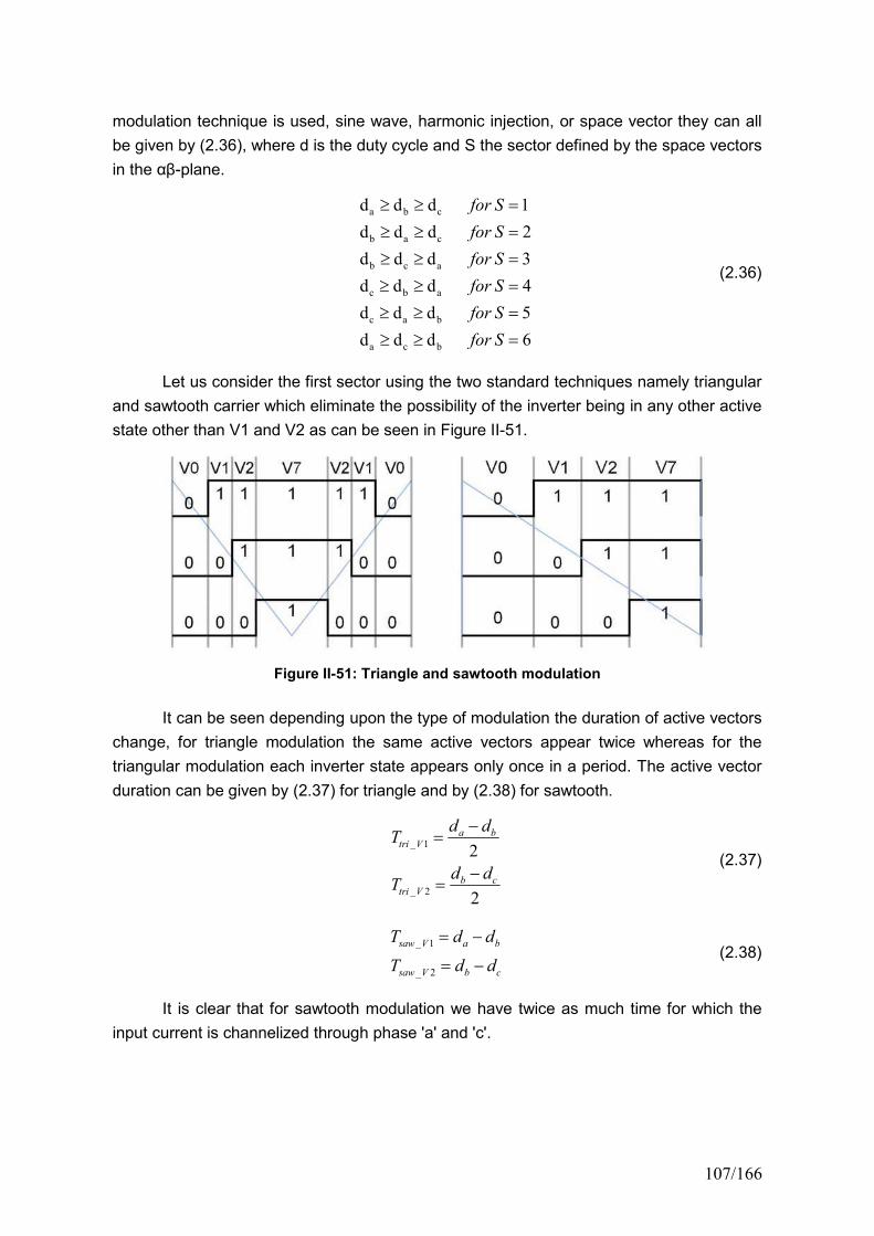
107/166
modulation technique is used, sine wave, harmonic injection, or space vector they can all
be given by (2.36), where d is the duty cycle and S the sector defined by the space vectors
in the αβ-plane.
a b c
b a c
b c a
c b a
c a b
a c b
d d d 1
d d d 2
d d d 3
d d d 4
d d d 5
d d d 6
for S
for S
for S
for S
for S
for S
(2.36)
Let us consider the first sector using the two standard techniques namely triangular
and sawtooth carrier which eliminate the possibility of the inverter being in any other active
state other than V1 and V2 as can be seen in Figure II-51.
Figure II-51: Triangle and sawtooth modulation
It can be seen depending upon the type of modulation the duration of active vectors
change, for triangle modulation the same active vectors appear twice whereas for the
triangular modulation each inverter state appears only once in a period. The active vector
duration can be given by (2.37) for triangle and by (2.38) for sawtooth.
_ 1
_ 2
2
2
a btri V
b ctri V
d dT
d dT
(2.37)
_ 1
_ 2
saw V a b
saw V b c
T d d
T d d
(2.38)
It is clear that for sawtooth modulation we have twice as much time for which the
input current is channelized through phase 'a' and 'c'.
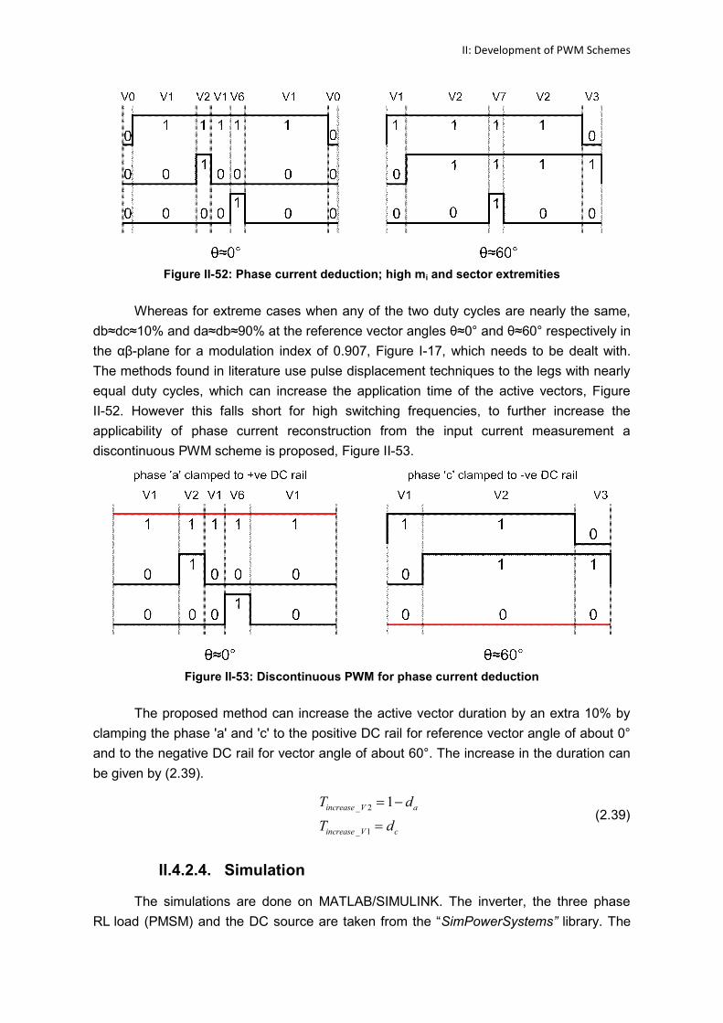
II: Development of PWM Schemes
Figure II-52: Phase current deduction; high mi and sector extremities
Whereas for extreme cases when any of the two duty cycles are nearly the same,
db≈dc≈10% and da≈db≈90% at the reference vector angles θ≈0° and θ≈60° respectively in the αβ-plane for a modulation index of 0.907, Figure I-17, which needs to be dealt with. The methods found in literature use pulse displacement techniques to the legs with nearly
equal duty cycles, which can increase the application time of the active vectors, Figure
II-52. However this falls short for high switching frequencies, to further increase the
applicability of phase current reconstruction from the input current measurement a
discontinuous PWM scheme is proposed, Figure II-53.
Figure II-53: Discontinuous PWM for phase current deduction
The proposed method can increase the active vector duration by an extra 10% by
clamping the phase 'a' and 'c' to the positive DC rail for reference vector angle of about 0°
and to the negative DC rail for vector angle of about 60°. The increase in the duration can
be given by (2.39).
_ 2
_ 1
1increase V a
increase V c
T d
T d
(2.39)
II.4.2.4. Simulation
The simulations are done on MATLAB/SIMULINK. The inverter, the three phase
RL load (PMSM) and the DC source are taken from the “SimPowerSystems” library. The
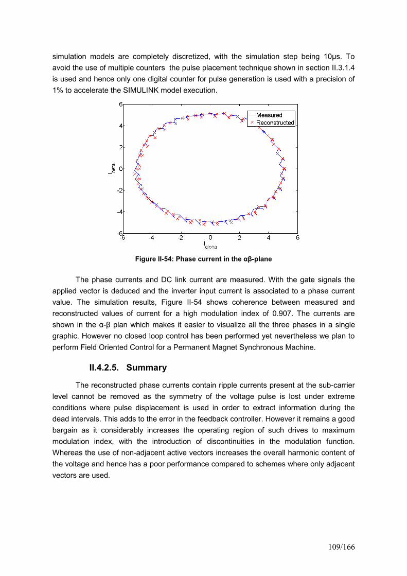
109/166
simulation models are completely discretized, with the simulation step being 10µs. To
avoid the use of multiple counters the pulse placement technique shown in section II.3.1.4
is used and hence only one digital counter for pulse generation is used with a precision of
1% to accelerate the SIMULINK model execution.
Figure II-54: Phase current in the αβ-plane
The phase currents and DC link current are measured. With the gate signals the
applied vector is deduced and the inverter input current is associated to a phase current
value. The simulation results, Figure II-54 shows coherence between measured and
reconstructed values of current for a high modulation index of 0.907. The currents are
shown in the α-β plan which makes it easier to visualize all the three phases in a single graphic. However no closed loop control has been performed yet nevertheless we plan to
perform Field Oriented Control for a Permanent Magnet Synchronous Machine.
II.4.2.5. Summary
The reconstructed phase currents contain ripple currents present at the sub-carrier
level cannot be removed as the symmetry of the voltage pulse is lost under extreme
conditions where pulse displacement is used in order to extract information during the
dead intervals. This adds to the error in the feedback controller. However it remains a good
bargain as it considerably increases the operating region of such drives to maximum
modulation index, with the introduction of discontinuities in the modulation function.
Whereas the use of non-adjacent active vectors increases the overall harmonic content of
the voltage and hence has a poor performance compared to schemes where only adjacent
vectors are used.
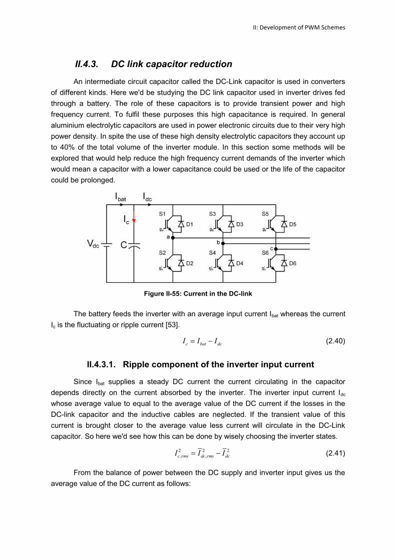
II: Development of PWM Schemes
II.4.3. DC link capacitor reduction
An intermediate circuit capacitor called the DC-Link capacitor is used in converters
of different kinds. Here we'd be studying the DC link capacitor used in inverter drives fed
through a battery. The role of these capacitors is to provide transient power and high
frequency current. To fulfil these purposes this high capacitance is required. In general
aluminium electrolytic capacitors are used in power electronic circuits due to their very high
power density. In spite the use of these high density electrolytic capacitors they account up
to 40% of the total volume of the inverter module. In this section some methods will be
explored that would help reduce the high frequency current demands of the inverter which
would mean a capacitor with a lower capacitance could be used or the life of the capacitor
could be prolonged.
Figure II-55: Current in the DC-link
The battery feeds the inverter with an average input current Ibat whereas the current
Ic is the fluctuating or ripple current [53].
c bat dcI I I (2.40)
II.4.3.1. Ripple component of the inverter input current
Since Ibat supplies a steady DC current the current circulating in the capacitor
depends directly on the current absorbed by the inverter. The inverter input current Idcwhose average value to equal to the average value of the DC current if the losses in the
DC-link capacitor and the inductive cables are neglected. If the transient value of this
current is brought closer to the average value less current will circulate in the DC-Link
capacitor. So here we'd see how this can be done by wisely choosing the inverter states.
2 2 2, ,c rms dc rms dcI I I (2.41)
From the balance of power between the DC supply and inverter input gives us the
average value of the DC current as follows:
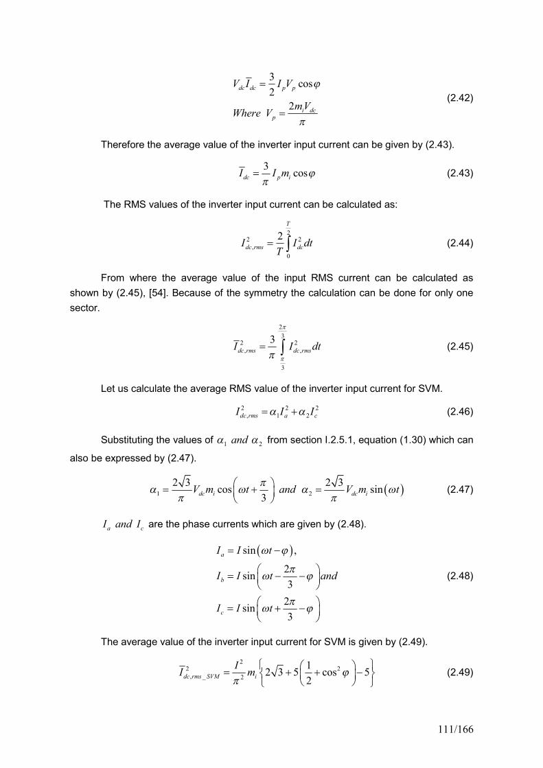
111/166
3cos
22
dc dc p p
i dcp
V I I V
mVWhere V
(2.42)
Therefore the average value of the inverter input current can be given by (2.43).
3cosdc p iI I m (2.43)
The RMS values of the inverter input current can be calculated as:
22 2,
0
2T
dc rms dcI I dtT
(2.44)
From where the average value of the input RMS current can be calculated as
shown by (2.45), [54]. Because of the symmetry the calculation can be done for only one
sector.
2
32 2, ,
3
3dc rms dc rmsI I dt
(2.45)
Let us calculate the average RMS value of the inverter input current for SVM.
2 2 2, 1 2dc rms a cI I I (2.46)
Substituting the values of 1 2and from section I.2.5.1, equation (1.30) which can
also be expressed by (2.47).
1 2
2 3 2 3cos sin
3dc i dc iV m t and V m t
(2.47)
a cI and I are the phase currents which are given by (2.48).
sin ,
2sin
3
2sin
3
a
b
c
I I t
I I t and
I I t
(2.48)
The average value of the inverter input current for SVM is given by (2.49).
22 2, _ 2
12 3 5 cos 5
2dc rms SVM i
II m
(2.49)
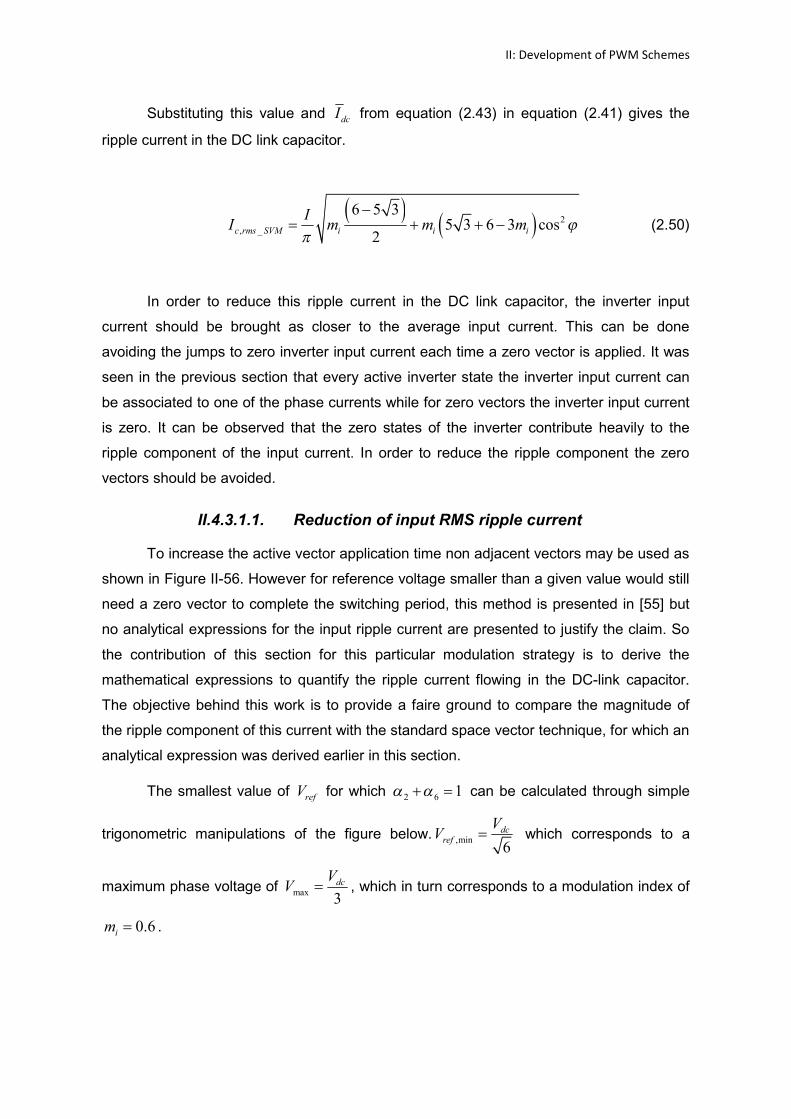
II: Development of PWM Schemes
Substituting this value and dcI from equation (2.43) in equation (2.41) gives the
ripple current in the DC link capacitor.
2, _
6 5 35 3 6 3 cos
2c rms SVM i i i
II m m m
(2.50)
In order to reduce this ripple current in the DC link capacitor, the inverter input
current should be brought as closer to the average input current. This can be done
avoiding the jumps to zero inverter input current each time a zero vector is applied. It was
seen in the previous section that every active inverter state the inverter input current can
be associated to one of the phase currents while for zero vectors the inverter input current
is zero. It can be observed that the zero states of the inverter contribute heavily to the
ripple component of the input current. In order to reduce the ripple component the zero
vectors should be avoided.
II.4.3.1.1. Reduction of input RMS ripple current
To increase the active vector application time non adjacent vectors may be used as
shown in Figure II-56. However for reference voltage smaller than a given value would still
need a zero vector to complete the switching period, this method is presented in [55] but
no analytical expressions for the input ripple current are presented to justify the claim. So
the contribution of this section for this particular modulation strategy is to derive the
mathematical expressions to quantify the ripple current flowing in the DC-link capacitor.
The objective behind this work is to provide a faire ground to compare the magnitude of
the ripple component of this current with the standard space vector technique, for which an
analytical expression was derived earlier in this section.
The smallest value of refV for which 2 6 1 can be calculated through simple
trigonometric manipulations of the figure below. ,min6dc
ref
VV which corresponds to a
maximum phase voltage of max 3dcVV , which in turn corresponds to a modulation index of
0.6im .
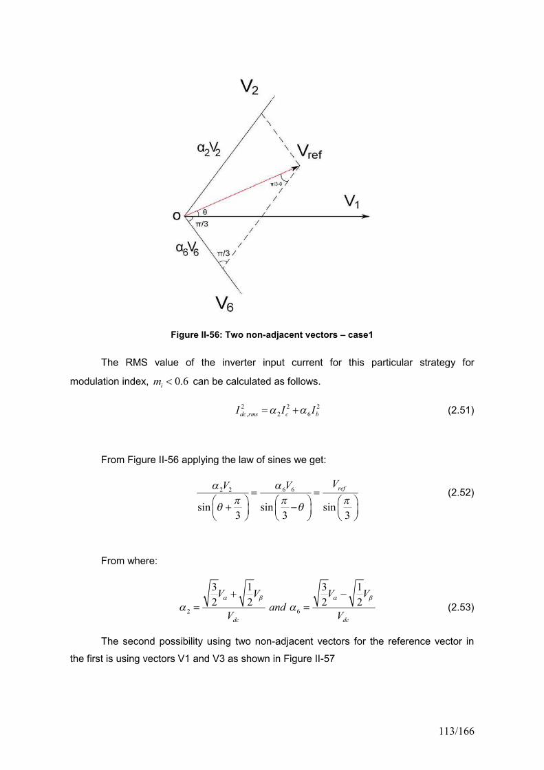
113/166
Figure II-56: Two non-adjacent vectors – case1
The RMS value of the inverter input current for this particular strategy for
modulation index, 0.6im can be calculated as follows.
2 2 2, 2 6dc rms c bI I I (2.51)
From Figure II-56 applying the law of sines we get:
6 62 2
sin sin sin3 3 3
refVVV
(2.52)
From where:
2 6
3 1 3 1
2 2 2 2
dc dc
V V V V
andV V
(2.53)
The second possibility using two non-adjacent vectors for the reference vector in
the first is using vectors V1 and V3 as shown in Figure II-57
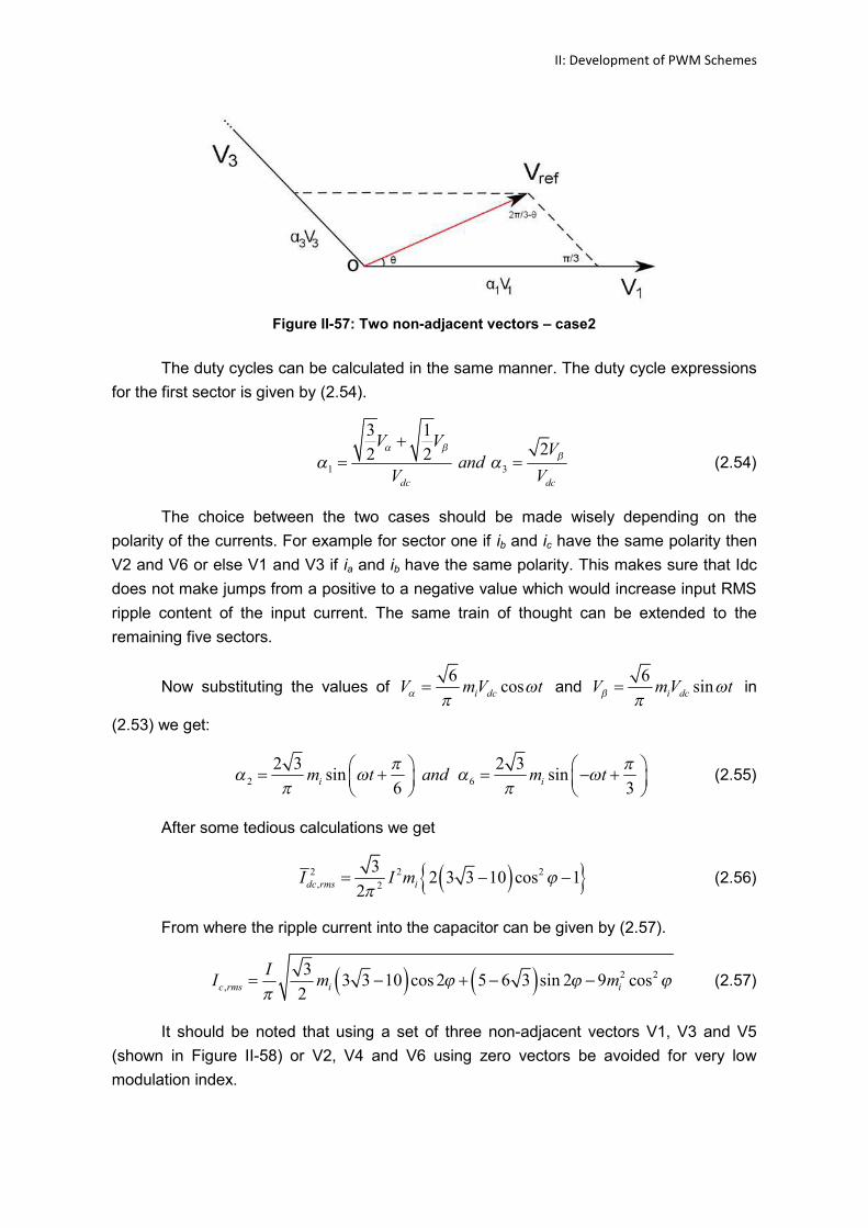
II: Development of PWM Schemes
Figure II-57: Two non-adjacent vectors – case2
The duty cycles can be calculated in the same manner. The duty cycle expressions
for the first sector is given by (2.54).
1 3
3 122 2
dc dc
V VV
andV V
(2.54)
The choice between the two cases should be made wisely depending on the
polarity of the currents. For example for sector one if ib and ic have the same polarity then
V2 and V6 or else V1 and V3 if ia and ib have the same polarity. This makes sure that Idc
does not make jumps from a positive to a negative value which would increase input RMS
ripple content of the input current. The same train of thought can be extended to the
remaining five sectors.
Now substituting the values of6
cosi dcV mV t and6
sini dcV mV t in
(2.53) we get:
2 6
2 3 2 3sin sin
6 3i im t and m t
(2.55)
After some tedious calculations we get
2 2 2, 2
32 3 3 10 cos 1
2dc rms iI I m (2.56)
From where the ripple current into the capacitor can be given by (2.57).
2 2,
33 3 10 cos 2 5 6 3 sin 2 9 cos
2c rms i i
II m m (2.57)
It should be noted that using a set of three non-adjacent vectors V1, V3 and V5
(shown in Figure II-58) or V2, V4 and V6 using zero vectors be avoided for very low
modulation index.
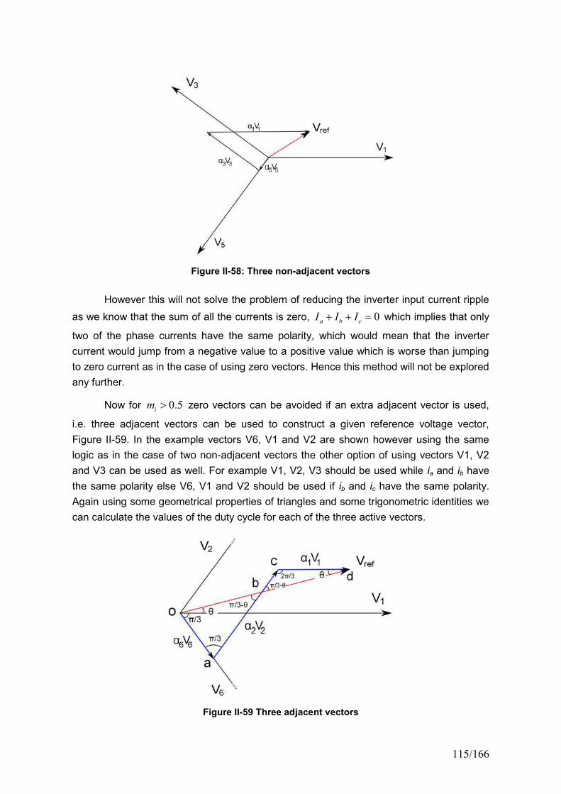
115/166
Figure II-58: Three non-adjacent vectors
However this will not solve the problem of reducing the inverter input current ripple
as we know that the sum of all the currents is zero, 0a b cI I I which implies that only
two of the phase currents have the same polarity, which would mean that the inverter
current would jump from a negative value to a positive value which is worse than jumping
to zero current as in the case of using zero vectors. Hence this method will not be explored
any further.
Now for 0.5im zero vectors can be avoided if an extra adjacent vector is used,
i.e. three adjacent vectors can be used to construct a given reference voltage vector,
Figure II-59. In the example vectors V6, V1 and V2 are shown however using the same
logic as in the case of two non-adjacent vectors the other option of using vectors V1, V2
and V3 can be used as well. For example V1, V2, V3 should be used while ia and ib have
the same polarity else V6, V1 and V2 should be used if ib and ic have the same polarity.
Again using some geometrical properties of triangles and some trigonometric identities we
can calculate the values of the duty cycle for each of the three active vectors.
Figure II-59 Three adjacent vectors
II: Development of PWM Schemes
Applying sine rule to triangles, oab and bdc we get (2.58) and (2.59)
respectively.
6 6
sin sin sin3 3 3
Vab ob
(2.58)
1 1
2 sinsin sin
3 3
V bd bc
(2.59)
Where 2 2 refV ab bc and V ob bd . Imposing 1 2 6 1 the
expressions for the duty cycles are given by the following expression, (2.60).
1 2
6
2 3 3 3 1sin , 1 cos sin
3
3cos 1 3 sin
m t m t t
and m t t
(2.60)
For a given sector k, 13
k in equations (2.58) and (2.59).
Equation (2.61) gives the expression for the average RMS current flowing in to the
inverter.
, 2 2 2
3 3 15 5 3 309 3 31 cos2 sin 2
2 4 4dc rms i i i
II m m m
(2.61)
From where the ripple current ,c rmsI into the capacitor can be given by calculated
subtracting the average input current, dcI given by equation (2.43) from the average input
RMS current, ,dc rmsI given by (2.61).
To compare the new technique of reduction of current stress on the capacitor with
the standard space vector method, In the Figure II-60 we've plotted the RMS ripple content
of the capacitor current, normalised with respect to the RMS values of the phase current
' I ', for the two cases for different values of the load angle and for the complete linear
range (0 to 0.907) of the modulation index 'mi'.

117/166
Figure II-60: RMS input current ripple
An abrupt decrease in the ripple component can be observed for the optimised
technique for 0.6im which represents the transition from the technique where two non-
adjacent active vectors along with 1 zero vector are used to the other technique where
only three adjacent active vectors are used.
In this section we successfully showed how the inverter input ripple current can be
reduced by modifying the PWM strategy. Now we'll study how it affects the input voltage.
II.4.3.2. Ripple component of the inverter input Voltage
Based on the same hypothesis that all the ripple component of the inverter input
current is absorbed by the DC link capacitor, the voltage across the capacitor can be given
by:
1c dc dcV I I dtC
(2.62)
The instantaneous value of the inverter input current depends on the state of the
inverter, we'll study the case where the reference vector falls in the first sector. The
calculations are made for the standard SVM where vectors V1 and V2 are used along with
the zero vectors, V0 and V7.
01 2
0 0 0
1TT T
c dc a dc c dcV I i dt I i dt I dtC
(2.63)
II: Development of PWM Schemes
Where 1 1 2 2 0 1 2,T T T T and T T T T and the vector duty cycles are
given by (2.47) for SVM. Now the mean square value of the ripple voltage over a PWM
period can be can be calculated as:
01 22 22 2 2 2 2
, 20 0 0
1TT T
c T dc a dc c dcV I i t dt I i t dt I t dtTC
(2.64)
Which leads to the following expression for the macroscopic mean ripple voltage:
22 232 2 3 3
, 1 2 1 221
3c T dc dc a dc c
TV I I i I i
C (2.65)
Now the average value of this voltage over a fundamental period can be calculated
as:
22 2, ,
6
3c rms c TV V d t
(2.66)
Upon some simplifying we obtain the final expression as:
2 2
2
32 22, 2
3
34 2 3
3 16
2 3 2 11 cos 2 3 4 5 3 11 sin16
5 21 3 15 3 243 3 3 cos 2 sin 2
10 10
dc
dcc rms
I k
I
I kT IV
C I
k
(2.67)
Where2 3
ik m .
Similarly for the optimised technique developed earlier in this section and we'd get
two separate expressions for m<0.6 and m>0.6, given by (2.68) and (2.69) respectively.
6 02
0 0 0
1T TT
c dc c dc b dcV I i dt I i dt I dtC
(2.68)
61 2
0 0 0
1TT T
c dc a dc c dc bV I i dt I i dt I i dtC
(2.69)
Where 2 2 6 6 0 2 6,T T T T and T T T T and
1 1 2 2 6 6,T T T T and T T given by equation (2.55) and (2.60) respectively.
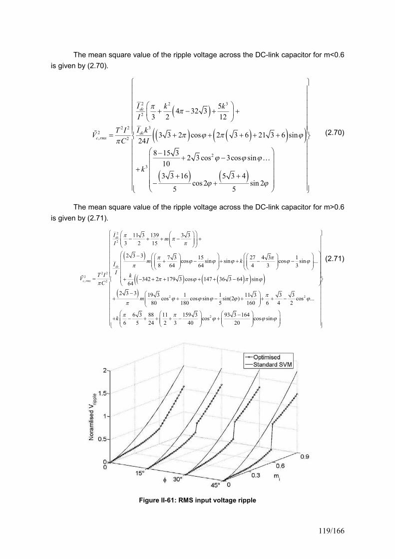
119/166
The mean square value of the ripple voltage across the DC-link capacitor for m<0.6
is given by (2.70).
2 2 3
2
32 22, 2
2
3
54 32 3
3 2 12
3 3 2 cos 2 3 6 21 3 6 sin24
8 15 32 3 cos 3cos sin
10
3 3 16 5 3 4cos 2 sin 2
5 5
dc
dcc rms
I k k
I
I kT IV
C I
k
(2.70)
The mean square value of the ripple voltage across the DC-link capacitor for m>0.6
is given by (2.71).
2
2
2 22, 2
11 3 139 3 3
3 2 15
2 3 3 7 3 15 27 4 3 1cos sin sin cos sin ...
8 64 64 4 3 3
342 2 179 3 cos 147 36 3 64 sin64
dc
dc
c rms
Im
I
m kI
IT I kV
C
2 2
2
2 3 3 19 3 1 1 11 3 3 3cos cos sin sin(2 ) cos ...
80 180 5 160 6 4 2
6 3 88 11 159 3 93 3 164cos cos sin
6 5 24 2 3 40 20
m
k
(2.71)
Figure II-61: RMS input voltage ripple
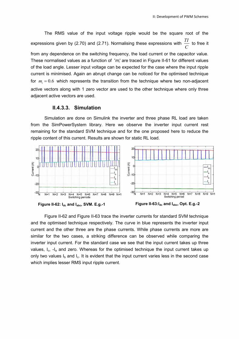
II: Development of PWM Schemes
The RMS value of the input voltage ripple would be the square root of the
expressions given by (2.70) and (2.71). Normalising these expressions withTI
Cto free it
from any dependence on the switching frequency, the load current or the capacitor value.
These normalised values as a function of 'mi' are traced in Figure II-61 for different values
of the load angle. Lesser input voltage can be expected for the case where the input ripple
current is minimised. Again an abrupt change can be noticed for the optimised technique
for 0.6im which represents the transition from the technique where two non-adjacent
active vectors along with 1 zero vector are used to the other technique where only three
adjacent active vectors are used.
II.4.3.3. Simulation
Simulation are done on Simulink the inverter and three phase RL load are taken
from the SimPowerSystem library. Here we observe the inverter input current rest
remaining for the standard SVM technique and for the one proposed here to reduce the
ripple content of this current. Results are shown for static RL load.
Figure II-62: Idc and Iabc, SVM. E.g.-1 Figure II-63:Idc and Iabc, Opt. E.g.-2
Figure II-62 and Figure II-63 trace the inverter currents for standard SVM technique
and the optimised technique respectively. The curve in blue represents the inverter input
current and the other three are the phase currents. While phase currents are more are
similar for the two cases, a striking difference can be observed while comparing the
inverter input current. For the standard case we see that the input current takes up three
values, Ic, -Ia and zero. Whereas for the optimised technique the input current takes up
only two values Ib and Ic. It is evident that the input current varies less in the second case
which implies lesser RMS input ripple current.
121/166
Figure II-64: Idc and Iabc, SVM. E.g.-2Figure II-65: Idc and Iabc, Opt. E.g.-2
Similarly another example is shown in Figure II-64, Figure II-65. While the phase
currents remain similar we can again notice stark difference in the inverter input currents.
For the standard case the input current again takes up three different values, Ia, -Ic and
zero. Whereas for the optimised technique it again takes up only values; -Ib and -Ic. It can
be easily said looking up at these two traces that there is less variation in the value of the
input current for the optimised current and hence a lower value of RMS ripple current.
II.4.3.4. Summary
In this section we studied the correlation between the PWM techniques and the
inverter input current. The objective of this study was to modify the PWM technique in so
that a smaller DC-link capacitor can be used. We saw that it is the DC-link capacitor which
feeds the inverter with the transient power and high frequency pulse currents whereas the
battery feeds the average inverter input. This pulse current is represented by the RMS
input current ripple.
Here we proposed some changes in the modulation strategy which attenuates the
demand of the inverter in terms of pulsed current. Performance wise there is one drawback
of this technique which is the increase of harmonic content in the output voltage. This
increase is due to the use of non-adjacent vectors. The effectiveness of these techniques
depends on the modulation index and the load angle. It is analytically shown that the
proposed techniques can decrease the input RMS ripple current by at least 20% under all
operating zones. Finally its repercussions on the ripple voltage are studied and lower ripple
content is observed for the proposed modulation strategy. These techniques are
complicated to implement. They require precise pulse placement. These techniques are
feedback techniques which require the current information or the load angle information to
make intelligent choices between different sets of vectors to be used.

PART III
EXPERIMENTAL VALIDATION
123/166
III.Experimental Validation
In order to validate the modulation strategies developed in earlier chapters they are
to be tested for closed loop electric drives for which they are destined. A versatile test
bench has to be developed in order to properly carry out the tests needed for validation not
only from a purely technical point of view but also evaluate its feasibility as an embeddable
solution. For this reason a new test platform with a digital signal processor (DSP) is
developed. A careful choice of DSP is made to be able to fulfil the needs of a digitally
controlled electric drive. Interfacing the Control Unit (DSP) with the Power Unit (electric
machine and inverter) is done through an electronic circuit which would condition and
scale the sensor output to levels acceptable to the ADC or binary ports of the DSP.
Similarly gate signals to control the inverter switches had to be adapted to levels
acceptable to the IGBT drivers. The experimental evaluation of the PWM schemes are
done on the data acquired through an oscilloscope to get a fine resolution, which are then
processed in Matlab.
III.1. Introduction
Test bench consists of a 20kW inverter, a PMSM and a DSP. The DSP is interfaced
with the inverter through a PCB. Standard vector controlled torque regulation strategy, the
Field Oriented Control (FOC) method is used to run the machine.
Figure III-1: Test bench, schematic diagram
III: Experimental Validation
III.2. Test bench
The experimental setup consists of a 20 kW, 3-phase 2-level IGBT inverter
designed for a nominal DC input voltage of 600 V with current and voltage sensors directly
mounted on the legs for stator current and line voltage measurements, a 3 kW PMSM with
an incremental encoder (4096 points), a 150 MHz Floating-Point DSP “TMS32F8335”, high
speed acquisition system, a buffer card for gate signal conditioning with incorporated dead
time. The test bench consists of two identical PM synchronous machines mechanically
coupled, one that is part of the system under observation is controlled and the other acts
as a load. In this section a detailed description of the test bench is given. The test setup is
divided into 3 parts the power unit, the control unit and an electronic unit to interface the
power and control unit.
III.2.1. Power Unit
This unit comprises of a three phase IGBT inverter, a Magna-PowerElectronics'
three phase full wave rectifier and a 'Leroy Somer' electric motor, 6 Pole surface mounted
permanent magnet sinusoidal synchronous motor (PMSM), with a nominal speed of
6000rpm and a maximum torque of 4.5Nm.
III.2.1.1. Power Converter -- VSI
The converter is a DC to AC three phase voltage source inverter. The maximum
inverter input voltage and current are 600V and 100Amps respectively. The maximum
rated power of the inverter is 20kW. The inverter can be switched till 30kHz.
Figure III-2: Inverter V-I characteristics
For these power ratings and switching frequencies IGBTs are better suited. Fuji
Electric Device and Technology IGBT modules are used, ref. no. 2MBI225U4N-120-50.
The different operating regions are graphically depicted in the Figure III-2, which shows
basically three boundary conditions where either the input voltage or the input current or
the input power reaches the maximum rated values. For e.g. for maximum rated voltage of
125/166
600V the input current should not exceed 33Amps to respect the inverter maximum power
ratings. The redline on the figure shows the different set of inverter voltage and current
values while respecting the inverter power ratings.
A
B
C
Water IN
+
_
Current Sensors
IGBT +Drivers
Inverter phases
DC Link
Water OUT
DC Bus Capacitor
Figure III-3: Inverter module
The maximum RMS phase voltage without pulse dropping is ~244V hence for
maximum power an RMS current of ~27Amps. The inverter is water cooled and each
inverter leg is equipped with a temperature sensor. The drivers are capable of detecting
short-circuits in case of inverter malfunction.
Figure III-4: IGBT Switching characteristics
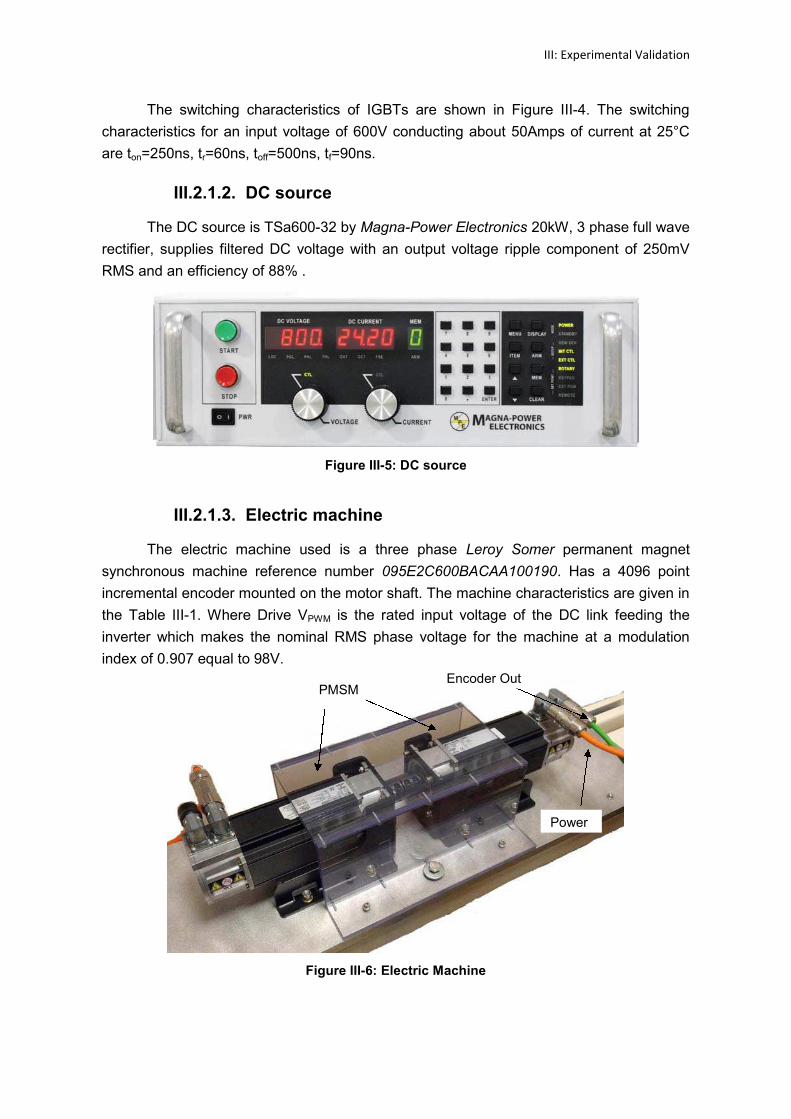
III: Experimental Validation
The switching characteristics of IGBTs are shown in Figure III-4. The switching
characteristics for an input voltage of 600V conducting about 50Amps of current at 25°C
are ton=250ns, tr=60ns, toff=500ns, tf=90ns.
III.2.1.2. DC source
The DC source is TSa600-32 by Magna-Power Electronics 20kW, 3 phase full wave
rectifier, supplies filtered DC voltage with an output voltage ripple component of 250mV
RMS and an efficiency of 88% .
Figure III-5: DC source
III.2.1.3. Electric machine
The electric machine used is a three phase Leroy Somer permanent magnet
synchronous machine reference number 095E2C600BACAA100190. Has a 4096 point
incremental encoder mounted on the motor shaft. The machine characteristics are given in
the Table III-1. Where Drive VPWM is the rated input voltage of the DC link feeding the
inverter which makes the nominal RMS phase voltage for the machine at a modulation
index of 0.907 equal to 98V.
Figure III-6: Electric Machine
PMSMEncoder Out
Power
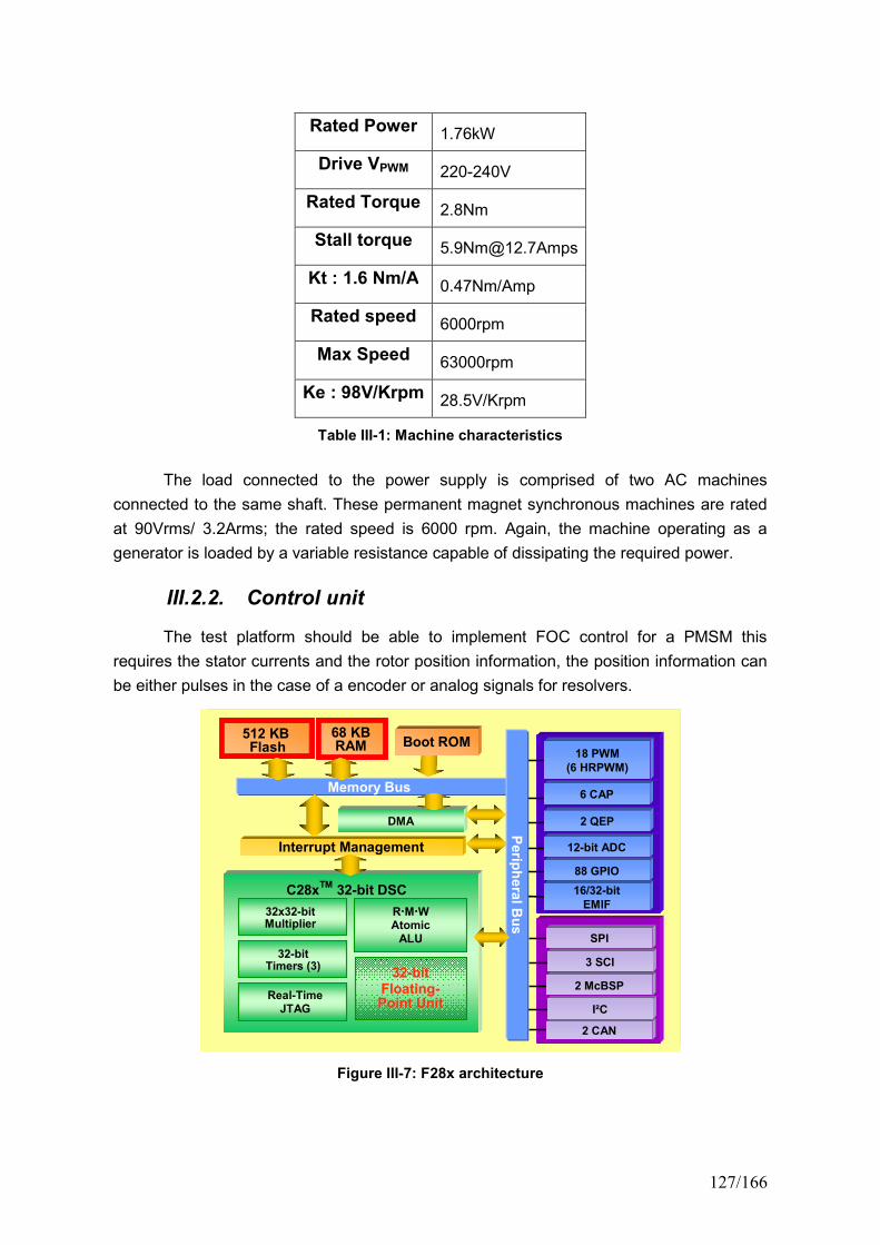
127/166
Rated Power 1.76kW
Drive VPWM 220-240V
Rated Torque 2.8Nm
Stall torque [email protected]
Kt : 1.6 Nm/A 0.47Nm/Amp
Rated speed 6000rpm
Max Speed 63000rpm
Ke : 98V/Krpm 28.5V/Krpm
Table III-1: Machine characteristics
The load connected to the power supply is comprised of two AC machines
connected to the same shaft. These permanent magnet synchronous machines are rated
at 90Vrms/ 3.2Arms; the rated speed is 6000 rpm. Again, the machine operating as a
generator is loaded by a variable resistance capable of dissipating the required power.
III.2.2. Control unit
The test platform should be able to implement FOC control for a PMSM this
requires the stator currents and the rotor position information, the position information can
be either pulses in the case of a encoder or analog signals for resolvers.
Real-TimeJTAG
32-bitTimers (3)
C28xTM 32-bit DSC
32x32-bitMultiplier
RMWAtomicALU
Interrupt Management
Memory Bus
12-bit ADC
SPI
2 CAN
3 SCI
2 McBSP
512 KBFlash
68 KBRAM
6 CAP
18 PWM(6 HRPWM)
DMA
3232--bitbitFloatingFloating--Point UnitPoint Unit
88 GPIO
I²C
Boot ROM
16/32-bitEMIF
2 QEP
Perip
heralBus
Real-TimeJTAG
Real-TimeJTAG
32-bitTimers (3)32-bit
Timers (3)
C28xTM 32-bit DSC
32x32-bitMultiplier
RMWAtomicALU
Interrupt Management
Memory Bus
12-bit ADC
SPI
2 CAN
3 SCI
2 McBSP
512 KBFlash512 KBFlash
68 KBRAM68 KBRAM
6 CAP
18 PWM(6 HRPWM)
DMA
3232--bitbitFloatingFloating--Point UnitPoint Unit
88 GPIO
I²C
Boot ROM
16/32-bitEMIF
2 QEP
Perip
heralBus
Figure III-7: F28x architecture
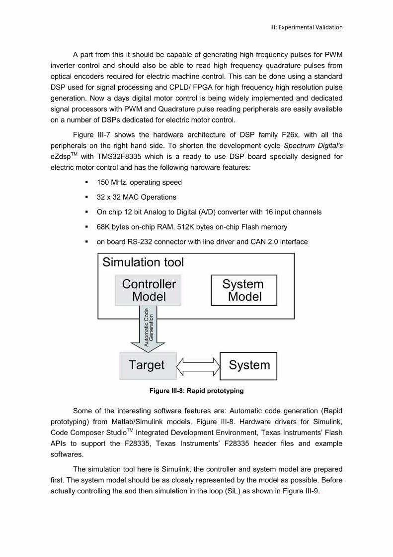
III: Experimental Validation
A part from this it should be capable of generating high frequency pulses for PWM
inverter control and should also be able to read high frequency quadrature pulses from
optical encoders required for electric machine control. This can be done using a standard
DSP used for signal processing and CPLD/ FPGA for high frequency high resolution pulse
generation. Now a days digital motor control is being widely implemented and dedicated
signal processors with PWM and Quadrature pulse reading peripherals are easily available
on a number of DSPs dedicated for electric motor control.
Figure III-7 shows the hardware architecture of DSP family F26x, with all the
peripherals on the right hand side. To shorten the development cycle Spectrum Digital's
eZdspTM with TMS32F8335 which is a ready to use DSP board specially designed for
electric motor control and has the following hardware features:
150 MHz. operating speed
32 x 32 MAC Operations
On chip 12 bit Analog to Digital (A/D) converter with 16 input channels
68K bytes on-chip RAM, 512K bytes on-chip Flash memory
on board RS-232 connector with line driver and CAN 2.0 interface
Figure III-8: Rapid prototyping
Some of the interesting software features are: Automatic code generation (Rapid
prototyping) from Matlab/Simulink models, Figure III-8. Hardware drivers for Simulink,
Code Composer StudioTM Integrated Development Environment, Texas Instruments’ Flash
APIs to support the F28335, Texas Instruments’ F28335 header files and example
softwares.
The simulation tool here is Simulink, the controller and system model are prepared
first. The system model should be as closely represented by the model as possible. Before
actually controlling the and then simulation in the loop (SiL) as shown in Figure III-9.
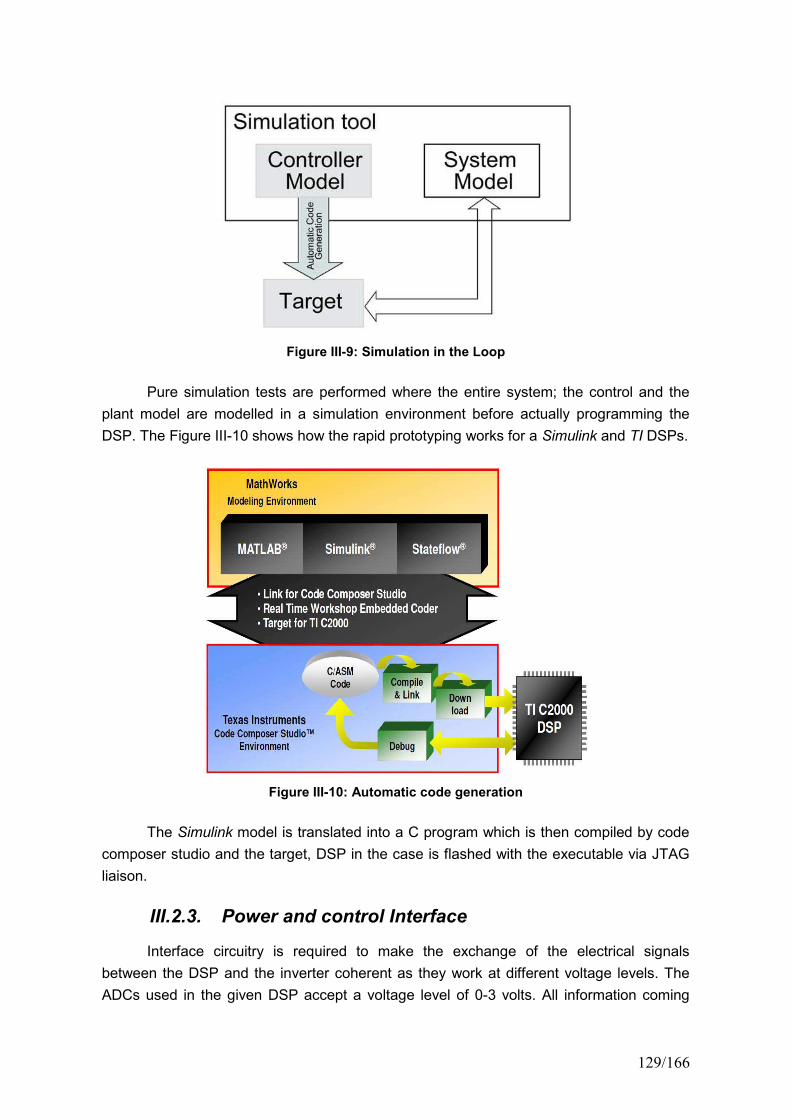
129/166
Figure III-9: Simulation in the Loop
Pure simulation tests are performed where the entire system; the control and the
plant model are modelled in a simulation environment before actually programming the
DSP. The Figure III-10 shows how the rapid prototyping works for a Simulink and TI DSPs.
Figure III-10: Automatic code generation
The Simulink model is translated into a C program which is then compiled by code
composer studio and the target, DSP in the case is flashed with the executable via JTAG
liaison.
III.2.3. Power and control Interface
Interface circuitry is required to make the exchange of the electrical signals
between the DSP and the inverter coherent as they work at different voltage levels. The
ADCs used in the given DSP accept a voltage level of 0-3 volts. All information coming
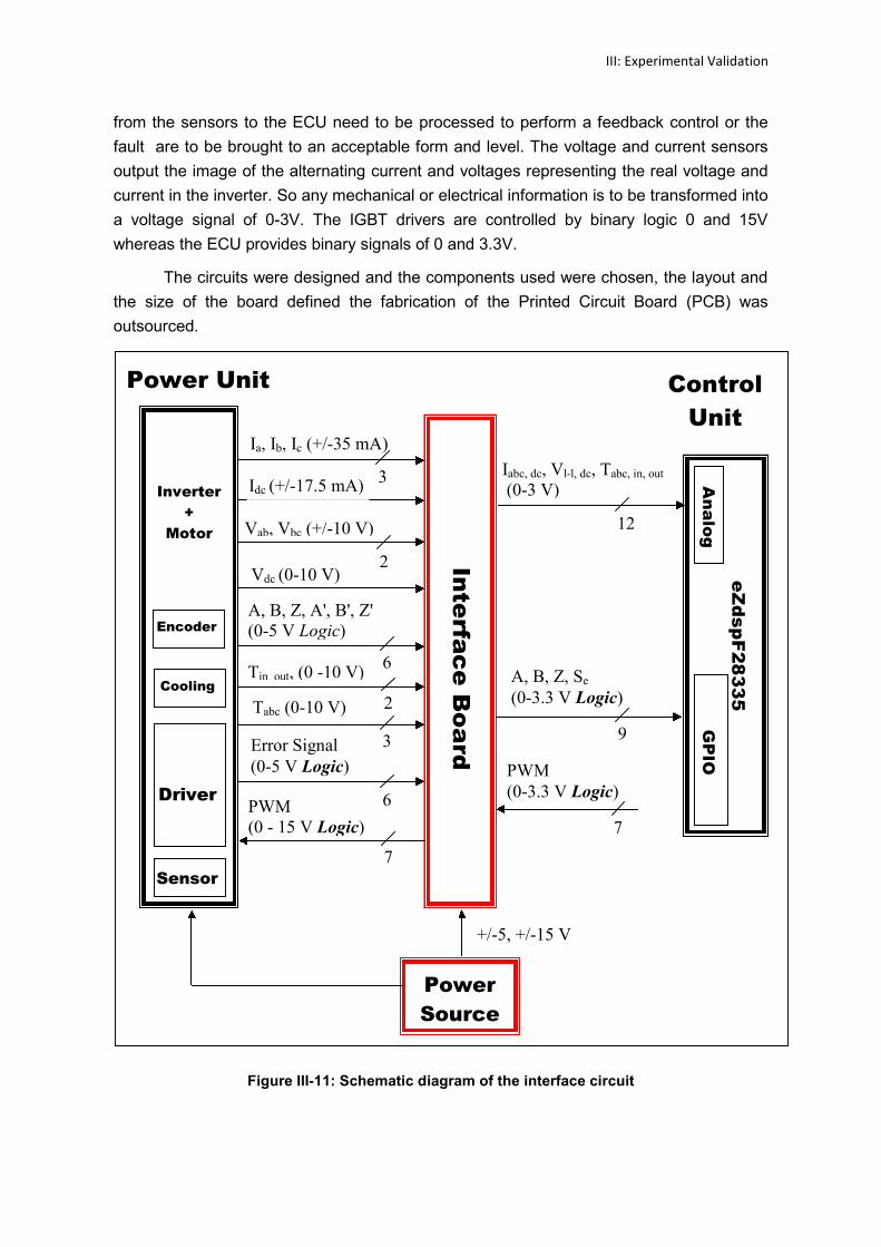
III: Experimental Validation
from the sensors to the ECU need to be processed to perform a feedback control or the
fault are to be brought to an acceptable form and level. The voltage and current sensors
output the image of the alternating current and voltages representing the real voltage and
current in the inverter. So any mechanical or electrical information is to be transformed into
a voltage signal of 0-3V. The IGBT drivers are controlled by binary logic 0 and 15V
whereas the ECU provides binary signals of 0 and 3.3V.
The circuits were designed and the components used were chosen, the layout and
the size of the board defined the fabrication of the Printed Circuit Board (PCB) was
outsourced.
Figure III-11: Schematic diagram of the interface circuit
Inverter
+
Motor
Interfa
ceBoard
eZdspF28335
Ia, Ib, Ic (+/-35 mA)
Idc (+/-17.5 mA)
Vab, Vbc (+/-10 V)
Vdc (0-10 V)
A, B, Z, A', B', Z'(0-5 V Logic)
6
3
2
GPIO
Analog
Error Signal(0-5 V Logic)
6
Iabc, dc, Vl-l, dc, Tabc, in, out(0-3 V)
12
A, B, Z, Se(0-3.3 V Logic)
9
Sensor
s
Power
Source
+/-5, +/-15 V
DriverPWM(0 - 15 V Logic)
7
PWM(0-3.3 V Logic)
7
Encoder
Tin_out, (0 -10 V)
2Tabc (0-10 V)
3
Cooling
Power Unit Control
Unit
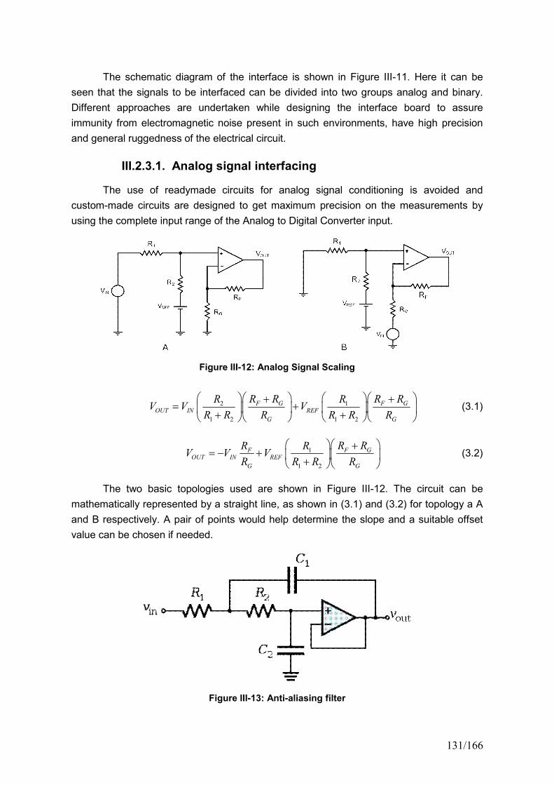
131/166
The schematic diagram of the interface is shown in Figure III-11. Here it can be
seen that the signals to be interfaced can be divided into two groups analog and binary.
Different approaches are undertaken while designing the interface board to assure
immunity from electromagnetic noise present in such environments, have high precision
and general ruggedness of the electrical circuit.
III.2.3.1. Analog signal interfacing
The use of readymade circuits for analog signal conditioning is avoided and
custom-made circuits are designed to get maximum precision on the measurements by
using the complete input range of the Analog to Digital Converter input.
Figure III-12: Analog Signal Scaling
2 1
1 2 1 2
F G F GOUT IN REF
G G
R R R RR RV V V
R R R R R R
(3.1)
1
1 2
F GFOUT IN REF
G G
R RR RV V V
R R R R
(3.2)
The two basic topologies used are shown in Figure III-12. The circuit can be
mathematically represented by a straight line, as shown in (3.1) and (3.2) for topology a A
and B respectively. A pair of points would help determine the slope and a suitable offset
value can be chosen if needed.
Figure III-13: Anti-aliasing filter
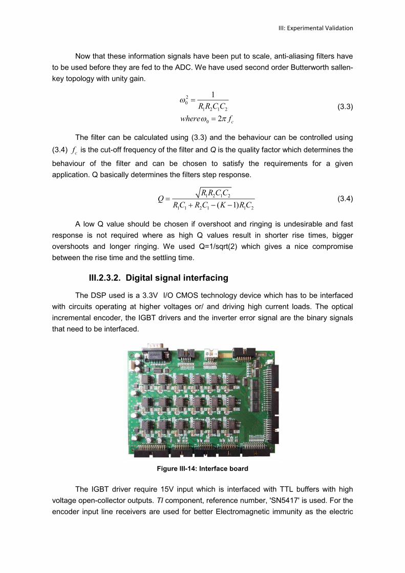
III: Experimental Validation
Now that these information signals have been put to scale, anti-aliasing filters have
to be used before they are fed to the ADC. We have used second order Butterworth sallen-
key topology with unity gain.
20
1 2 1 2
0
1
2 c
R R C C
where f
(3.3)
The filter can be calculated using (3.3) and the behaviour can be controlled using
(3.4) cf is the cut-off frequency of the filter and Q is the quality factor which determines the
behaviour of the filter and can be chosen to satisfy the requirements for a given
application. Q basically determines the filters step response.
1 2 1 2
1 1 2 1 1 2( 1)
R R C CQ
RC R C K RC (3.4)
A low Q value should be chosen if overshoot and ringing is undesirable and fast
response is not required where as high Q values result in shorter rise times, bigger
overshoots and longer ringing. We used Q=1/sqrt(2) which gives a nice compromise
between the rise time and the settling time.
III.2.3.2. Digital signal interfacing
The DSP used is a 3.3V I/O CMOS technology device which has to be interfaced
with circuits operating at higher voltages or/ and driving high current loads. The optical
incremental encoder, the IGBT drivers and the inverter error signal are the binary signals
that need to be interfaced.
Figure III-14: Interface board
The IGBT driver require 15V input which is interfaced with TTL buffers with high
voltage open-collector outputs. TI component, reference number, 'SN5417' is used. For the
encoder input line receivers are used for better Electromagnetic immunity as the electric
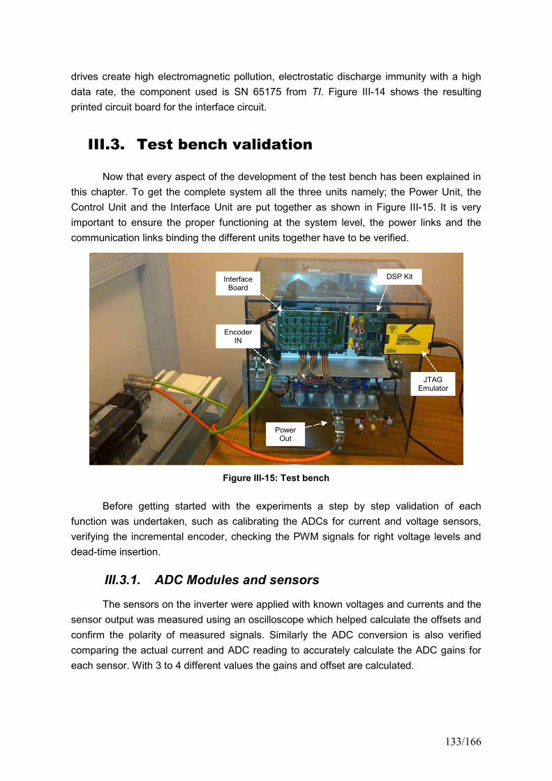
133/166
drives create high electromagnetic pollution, electrostatic discharge immunity with a high
data rate, the component used is SN 65175 from TI. Figure III-14 shows the resulting
printed circuit board for the interface circuit.
III.3. Test bench validation
Now that every aspect of the development of the test bench has been explained in
this chapter. To get the complete system all the three units namely; the Power Unit, the
Control Unit and the Interface Unit are put together as shown in Figure III-15. It is very
important to ensure the proper functioning at the system level, the power links and the
communication links binding the different units together have to be verified.
Figure III-15: Test bench
Before getting started with the experiments a step by step validation of each
function was undertaken, such as calibrating the ADCs for current and voltage sensors,
verifying the incremental encoder, checking the PWM signals for right voltage levels and
dead-time insertion.
III.3.1. ADC Modules and sensors
The sensors on the inverter were applied with known voltages and currents and the
sensor output was measured using an oscilloscope which helped calculate the offsets and
confirm the polarity of measured signals. Similarly the ADC conversion is also verified
comparing the actual current and ADC reading to accurately calculate the ADC gains for
each sensor. With 3 to 4 different values the gains and offset are calculated.
JTAGEmulator
InterfaceBoard
DSP Kit
PowerOut
EncoderIN
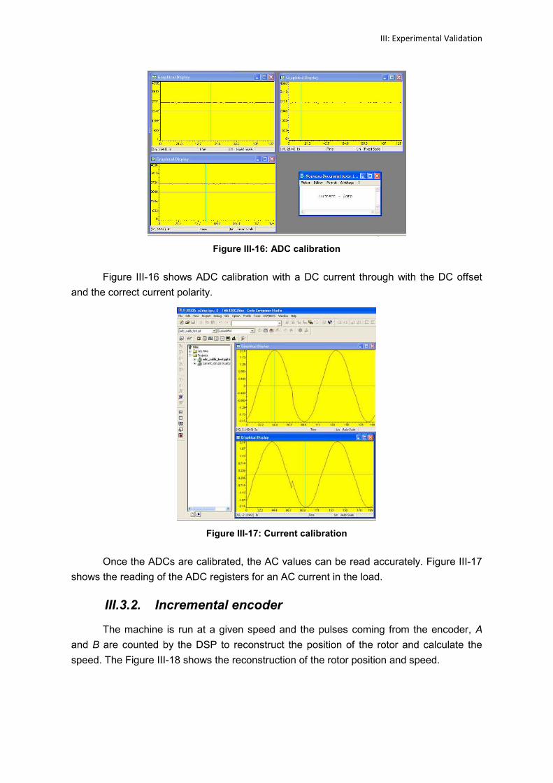
III: Experimental Validation
Figure III-16: ADC calibration
Figure III-16 shows ADC calibration with a DC current through with the DC offset
and the correct current polarity.
Figure III-17: Current calibration
Once the ADCs are calibrated, the AC values can be read accurately. Figure III-17
shows the reading of the ADC registers for an AC current in the load.
III.3.2. Incremental encoder
The machine is run at a given speed and the pulses coming from the encoder, A
and B are counted by the DSP to reconstruct the position of the rotor and calculate the
speed. The Figure III-18 shows the reconstruction of the rotor position and speed.

135/166
Figure III-18: Encoder verification
III.3.3. PWM Module
The PWM signals are verified at the DSP output and at the driver input with a
constant duty cycle and a given dead-time.
Figure III-19: PWM signals from DSP
These tests are very helpful to the test bench and validate the interfacing of the
power unit and control unit. This confirms good functioning of the bench.
III.4. Performance indicators
The test bench is fully functional and before we start comparing the different
modulation strategies we need to decide upon the performance indicators that should be
used. We'd like to compare these techniques on three grounds, the harmonic content of
the modulated voltage, the frequency spectrum and the switching losses.
The waveform quality or the harmonic content is compared in terms of Harmonic
Distortion Factor (HDF) /Weighted Total Harmonic Distortion (WTHD), whereas HDF is
better suited for comparing the performance analytically whereas WTHD is better suited
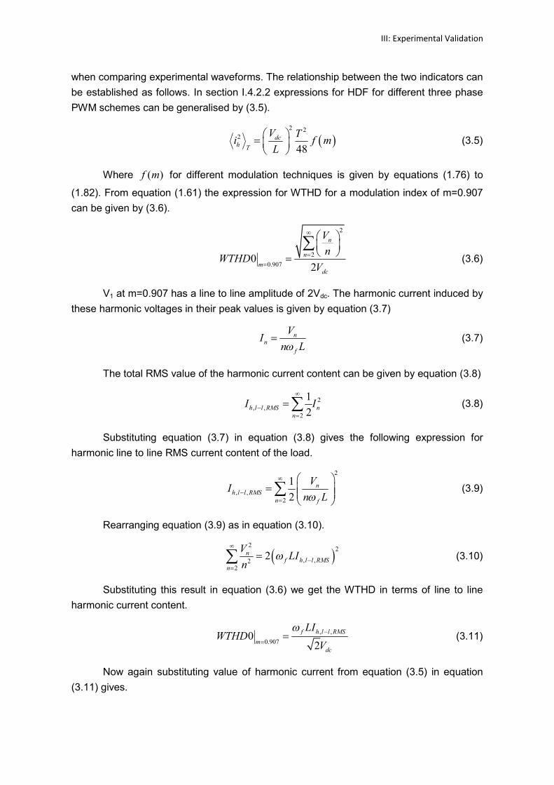
III: Experimental Validation
when comparing experimental waveforms. The relationship between the two indicators can
be established as follows. In section I.4.2.2 expressions for HDF for different three phase
PWM schemes can be generalised by (3.5).
2 22
48dc
hT
V Ti f m
L
(3.5)
Where ( )f m for different modulation techniques is given by equations (1.76) to
(1.82). From equation (1.61) the expression for WTHD for a modulation index of m=0.907
can be given by (3.6).
2
2
0.9070
2
n
n
mdc
V
nWTHD
V
(3.6)
V1 at m=0.907 has a line to line amplitude of 2Vdc. The harmonic current induced by
these harmonic voltages in their peak values is given by equation (3.7)
nn
f
VI
n L (3.7)
The total RMS value of the harmonic current content can be given by equation (3.8)
2, ,
2
1
2h l l RMS n
n
I I
(3.8)
Substituting equation (3.7) in equation (3.8) gives the following expression for
harmonic line to line RMS current content of the load.
2
, ,2
1
2n
h l l RMS
n f
VI
n L
(3.9)
Rearranging equation (3.9) as in equation (3.10).
22
, ,22
2nf h l l RMS
n
VLI
n
(3.10)
Substituting this result in equation (3.6) we get the WTHD in terms of line to line
harmonic current content.
, ,
0.9070
2
f h l l RMS
m
dc
LIWTHD
V
(3.11)
Now again substituting value of harmonic current from equation (3.5) in equation
(3.11) gives.
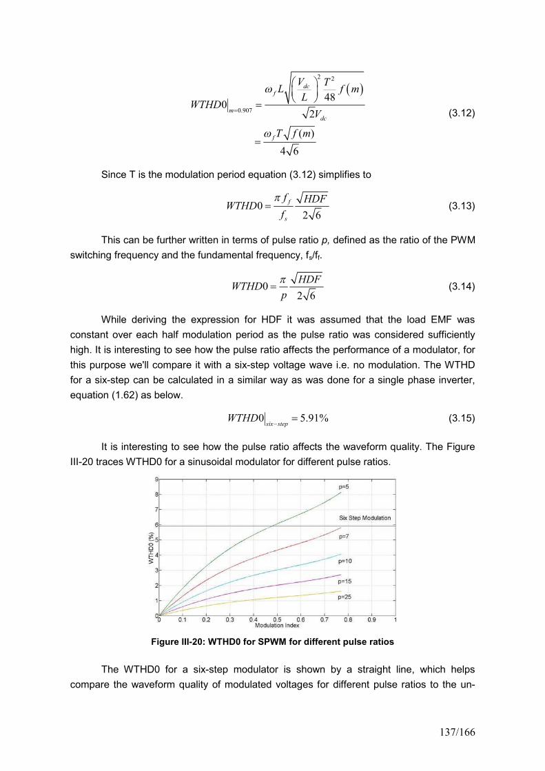
137/166
2 2
0.907
480
2
( )
4 6
dcf
m
dc
f
V TL f m
LWTHD
V
T f m
(3.12)
Since T is the modulation period equation (3.12) simplifies to
02 6
f
s
f HDFWTHD
f
(3.13)
This can be further written in terms of pulse ratio p, defined as the ratio of the PWM
switching frequency and the fundamental frequency, fs/ff.
02 6
HDFWTHD
p
(3.14)
While deriving the expression for HDF it was assumed that the load EMF was
constant over each half modulation period as the pulse ratio was considered sufficiently
high. It is interesting to see how the pulse ratio affects the performance of a modulator, for
this purpose we'll compare it with a six-step voltage wave i.e. no modulation. The WTHD
for a six-step can be calculated in a similar way as was done for a single phase inverter,
equation (1.62) as below.
0 5.91%six step
WTHD (3.15)
It is interesting to see how the pulse ratio affects the waveform quality. The Figure
III-20 traces WTHD0 for a sinusoidal modulator for different pulse ratios.
Figure III-20: WTHD0 for SPWM for different pulse ratios
The WTHD0 for a six-step modulator is shown by a straight line, which helps
compare the waveform quality of modulated voltages for different pulse ratios to the un-
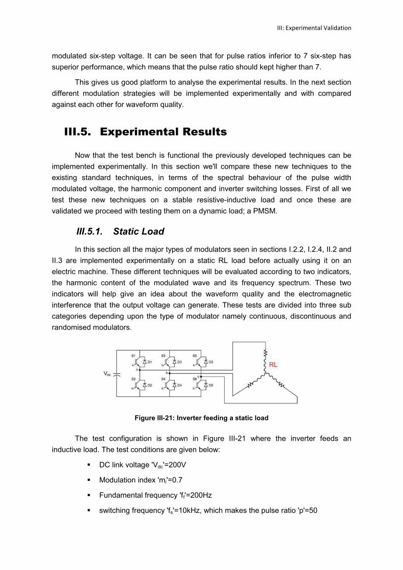
III: Experimental Validation
modulated six-step voltage. It can be seen that for pulse ratios inferior to 7 six-step has
superior performance, which means that the pulse ratio should kept higher than 7.
This gives us good platform to analyse the experimental results. In the next section
different modulation strategies will be implemented experimentally and with compared
against each other for waveform quality.
III.5. Experimental Results
Now that the test bench is functional the previously developed techniques can be
implemented experimentally. In this section we'll compare these new techniques to the
existing standard techniques, in terms of the spectral behaviour of the pulse width
modulated voltage, the harmonic component and inverter switching losses. First of all we
test these new techniques on a stable resistive-inductive load and once these are
validated we proceed with testing them on a dynamic load; a PMSM.
III.5.1. Static Load
In this section all the major types of modulators seen in sections I.2.2, I.2.4, II.2 and
II.3 are implemented experimentally on a static RL load before actually using it on an
electric machine. These different techniques will be evaluated according to two indicators,
the harmonic content of the modulated wave and its frequency spectrum. These two
indicators will help give an idea about the waveform quality and the electromagnetic
interference that the output voltage can generate. These tests are divided into three sub
categories depending upon the type of modulator namely continuous, discontinuous and
randomised modulators.
Figure III-21: Inverter feeding a static load
The test configuration is shown in Figure III-21 where the inverter feeds an
inductive load. The test conditions are given below:
DC link voltage 'Vdc'=200V
Modulation index 'mi'=0.7
Fundamental frequency 'ff'=200Hz
switching frequency 'fs'=10kHz, which makes the pulse ratio 'p'=50
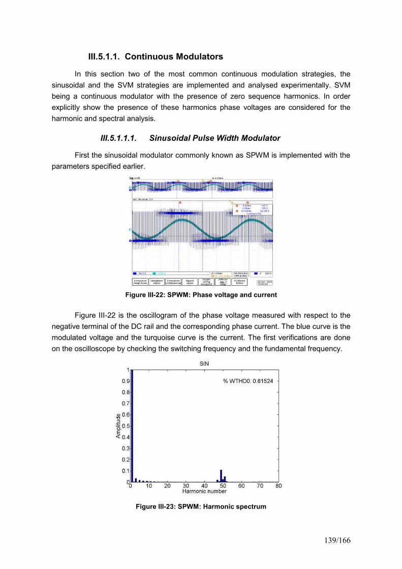
139/166
III.5.1.1. Continuous Modulators
In this section two of the most common continuous modulation strategies, the
sinusoidal and the SVM strategies are implemented and analysed experimentally. SVM
being a continuous modulator with the presence of zero sequence harmonics. In order
explicitly show the presence of these harmonics phase voltages are considered for the
harmonic and spectral analysis.
III.5.1.1.1. Sinusoidal Pulse Width Modulator
First the sinusoidal modulator commonly known as SPWM is implemented with the
parameters specified earlier.
Figure III-22: SPWM: Phase voltage and current
Figure III-22 is the oscillogram of the phase voltage measured with respect to the
negative terminal of the DC rail and the corresponding phase current. The blue curve is the
modulated voltage and the turquoise curve is the current. The first verifications are done
on the oscilloscope by checking the switching frequency and the fundamental frequency.
Figure III-23: SPWM: Harmonic spectrum
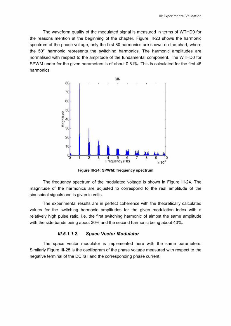
III: Experimental Validation
The waveform quality of the modulated signal is measured in terms of WTHD0 for
the reasons mention at the beginning of the chapter. Figure III-23 shows the harmonic
spectrum of the phase voltage, only the first 80 harmonics are shown on the chart, where
the 50th harmonic represents the switching harmonics. The harmonic amplitudes are
normalised with respect to the amplitude of the fundamental component. The WTHD0 for
SPWM under for the given parameters is of about 0.81%. This is calculated for the first 45
harmonics.
Figure III-24: SPWM: frequency spectrum
The frequency spectrum of the modulated voltage is shown in Figure III-24. The
magnitude of the harmonics are adjusted to correspond to the real amplitude of the
sinusoidal signals and is given in volts.
The experimental results are in perfect coherence with the theoretically calculated
values for the switching harmonic amplitudes for the given modulation index with a
relatively high pulse ratio, i.e. the first switching harmonic of almost the same amplitude
with the side bands being about 30% and the second harmonic being about 40%.
III.5.1.1.2. Space Vector Modulator
The space vector modulator is implemented here with the same parameters.
Similarly Figure III-25 is the oscillogram of the phase voltage measured with respect to the
negative terminal of the DC rail and the corresponding phase current.
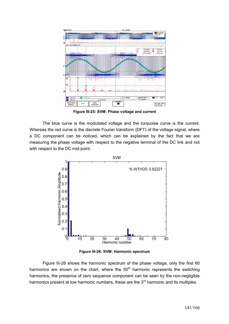
141/166
Figure III-25: SVM: Phase voltage and current
The blue curve is the modulated voltage and the turquoise curve is the current.
Whereas the red curve is the discrete Fourier transform (DFT) of the voltage signal, where
a DC component can be noticed, which can be explained by the fact that we are
measuring the phase voltage with respect to the negative terminal of the DC link and not
with respect to the DC mid-point.
Figure III-26: SVM: Harmonic spectrum
Figure III-26 shows the harmonic spectrum of the phase voltage, only the first 80
harmonics are shown on the chart, where the 50th harmonic represents the switching
harmonics, the presence of zero sequence component can be seen by the non-negligible
harmonics present at low harmonic numbers, these are the 3rd harmonic and its multiples.
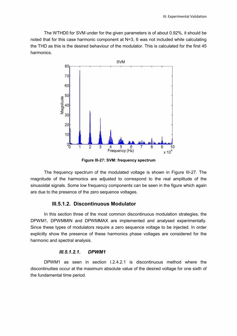
III: Experimental Validation
The WTHD0 for SVM under for the given parameters is of about 0.92%, it should be
noted that for this case harmonic component at N=3, 6 was not included while calculating
the THD as this is the desired behaviour of the modulator. This is calculated for the first 45
harmonics.
Figure III-27: SVM: frequency spectrum
The frequency spectrum of the modulated voltage is shown in Figure III-27. The
magnitude of the harmonics are adjusted to correspond to the real amplitude of the
sinusoidal signals. Some low frequency components can be seen in the figure which again
are due to the presence of the zero sequence voltages.
III.5.1.2. Discontinuous Modulator
In this section three of the most common discontinuous modulation strategies, the
DPWM1, DPWMMIN and DPWMMAX are implemented and analysed experimentally.
Since these types of modulators require a zero sequence voltage to be injected. In order
explicitly show the presence of these harmonics phase voltages are considered for the
harmonic and spectral analysis.
III.5.1.2.1. DPWM1
DPWM1 as seen in section I.2.4.2.1 is discontinuous method where the
discontinuities occur at the maximum absolute value of the desired voltage for one sixth of
the fundamental time period.
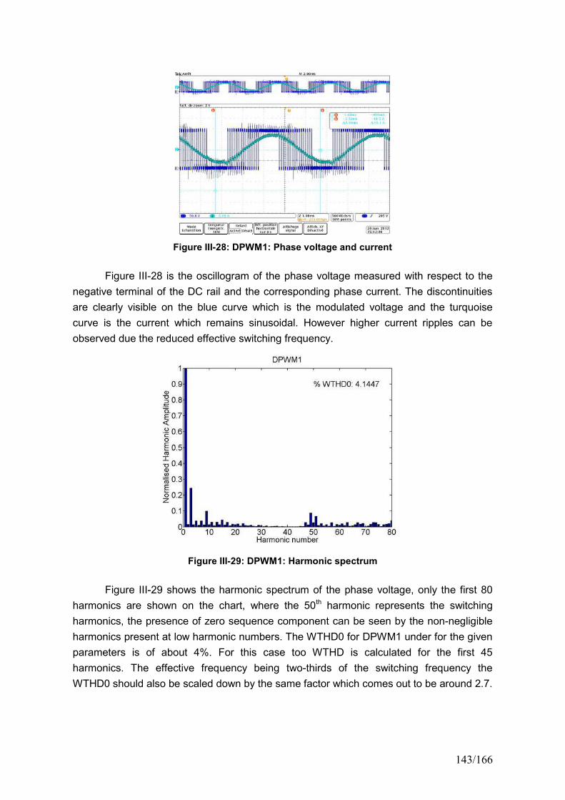
143/166
Figure III-28: DPWM1: Phase voltage and current
Figure III-28 is the oscillogram of the phase voltage measured with respect to the
negative terminal of the DC rail and the corresponding phase current. The discontinuities
are clearly visible on the blue curve which is the modulated voltage and the turquoise
curve is the current which remains sinusoidal. However higher current ripples can be
observed due the reduced effective switching frequency.
Figure III-29: DPWM1: Harmonic spectrum
Figure III-29 shows the harmonic spectrum of the phase voltage, only the first 80
harmonics are shown on the chart, where the 50th harmonic represents the switching
harmonics, the presence of zero sequence component can be seen by the non-negligible
harmonics present at low harmonic numbers. The WTHD0 for DPWM1 under for the given
parameters is of about 4%. For this case too WTHD is calculated for the first 45
harmonics. The effective frequency being two-thirds of the switching frequency the
WTHD0 should also be scaled down by the same factor which comes out to be around 2.7.
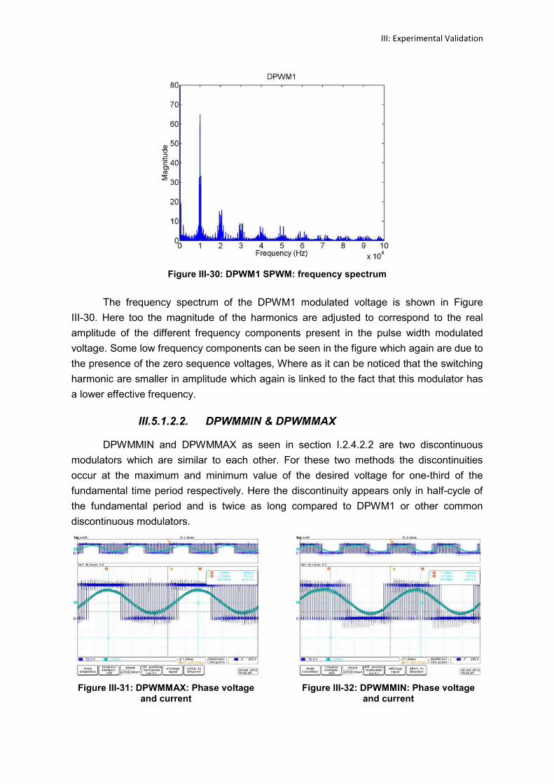
III: Experimental Validation
Figure III-30: DPWM1 SPWM: frequency spectrum
The frequency spectrum of the DPWM1 modulated voltage is shown in Figure
III-30. Here too the magnitude of the harmonics are adjusted to correspond to the real
amplitude of the different frequency components present in the pulse width modulated
voltage. Some low frequency components can be seen in the figure which again are due to
the presence of the zero sequence voltages, Where as it can be noticed that the switching
harmonic are smaller in amplitude which again is linked to the fact that this modulator has
a lower effective frequency.
III.5.1.2.2. DPWMMIN & DPWMMAX
DPWMMIN and DPWMMAX as seen in section I.2.4.2.2 are two discontinuous
modulators which are similar to each other. For these two methods the discontinuities
occur at the maximum and minimum value of the desired voltage for one-third of the
fundamental time period respectively. Here the discontinuity appears only in half-cycle of
the fundamental period and is twice as long compared to DPWM1 or other common
discontinuous modulators.
Figure III-31: DPWMMAX: Phase voltageand current
Figure III-32: DPWMMIN: Phase voltageand current
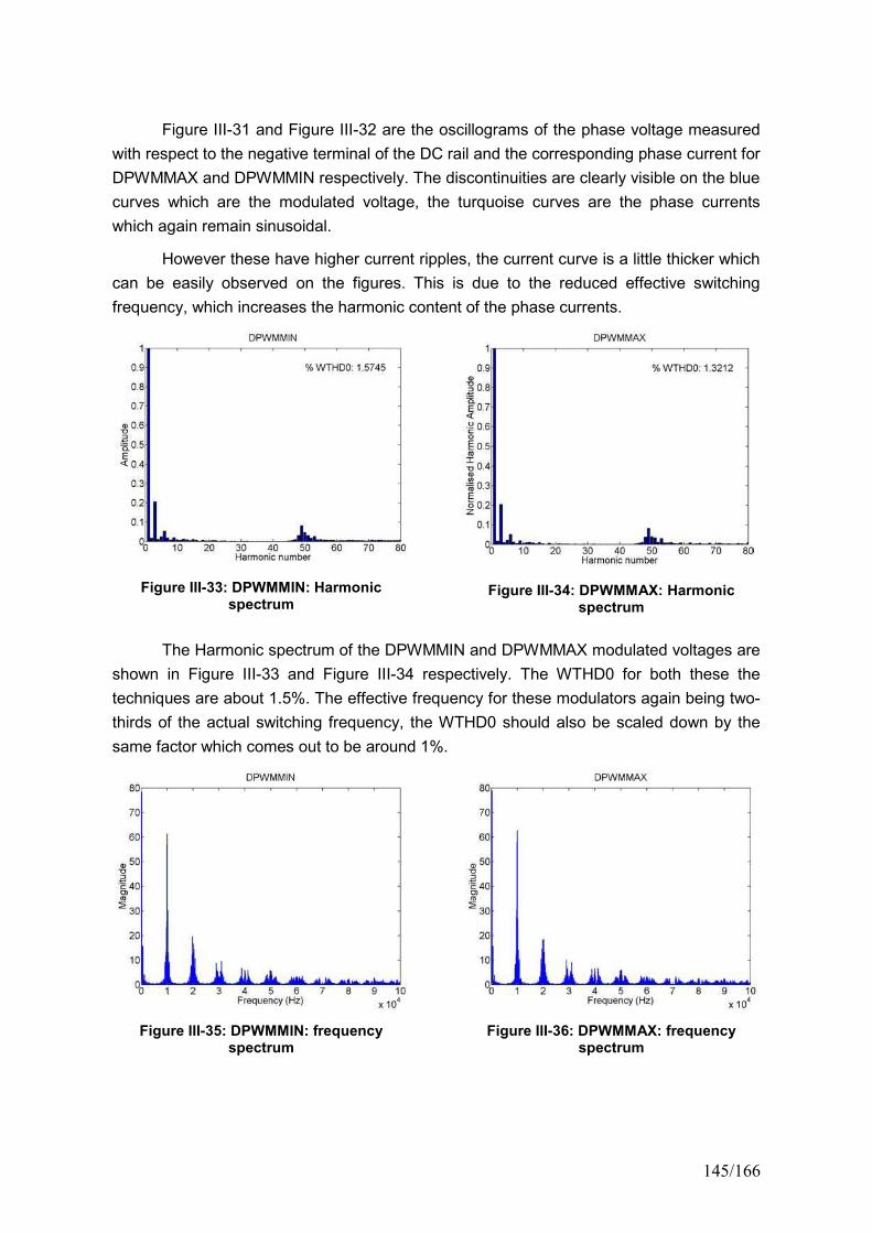
145/166
Figure III-31 and Figure III-32 are the oscillograms of the phase voltage measured
with respect to the negative terminal of the DC rail and the corresponding phase current for
DPWMMAX and DPWMMIN respectively. The discontinuities are clearly visible on the blue
curves which are the modulated voltage, the turquoise curves are the phase currents
which again remain sinusoidal.
However these have higher current ripples, the current curve is a little thicker which
can be easily observed on the figures. This is due to the reduced effective switching
frequency, which increases the harmonic content of the phase currents.
Figure III-33: DPWMMIN: Harmonicspectrum
Figure III-34: DPWMMAX: Harmonicspectrum
The Harmonic spectrum of the DPWMMIN and DPWMMAX modulated voltages are
shown in Figure III-33 and Figure III-34 respectively. The WTHD0 for both these the
techniques are about 1.5%. The effective frequency for these modulators again being two-
thirds of the actual switching frequency, the WTHD0 should also be scaled down by the
same factor which comes out to be around 1%.
Figure III-35: DPWMMIN: frequencyspectrum
Figure III-36: DPWMMAX: frequencyspectrum

III: Experimental Validation
The frequency spectrum of the DPWMMIN and DPWMMAX modulated voltages are
shown in Figure III-35 and Figure III-36 respectively. Here too the magnitude of the
harmonics are adjusted to correspond to the real amplitude of the different frequency
components present in the pulse width modulated voltage. Some low frequency
components can be seen in the figure which again are due to the presence of the zero
sequence voltages, whereas it can again be noticed that the switching harmonics are
smaller in amplitude which again is linked to the fact that this modulator has a lower
effective frequency. Hence we obtain expected results.
III.5.1.3. Random modulator
A random space vector modulator of section II.3.3 which is basically a random
carrier frequency type modulator, is implemented in this section and is compared to the
standard deterministic modulator. The randomisation factor of 0.2 was taken with a
statistically expected value of the switching frequency being 10kHz, this will make the
switching frequency vary randomly between 9 and 11kHz.
Figure III-37: SVM: Phase voltage andcurrent
Figure III-38: RSVM: Phase voltage andcurrent
The oscillograms, Figure III-37 and Figure III-38 for deterministic SVM and
randomised SVM are put side by side to so that their frequency spectrum can be
compared easily. The blue curve is the modulated voltage and the turquoise curve is the
current. Whereas the red curve is the discrete Fourier transform (DFT) of the voltage
signal, where a DC component can be noticed, which can be explained by the fact that we
are measuring the phase voltage with respect to the negative terminal of the DC link and
not with respect to the DC mid-point. The first switching harmonic for deterministic SVM
has an amplitude of 54V whereas for the randomised SVM the amplitude is of 20V. This a
significant reduction in the peak harmonic values.
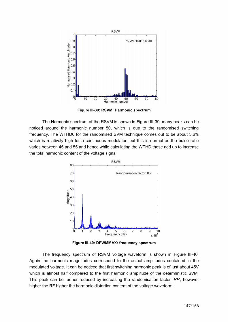
147/166
Figure III-39: RSVM: Harmonic spectrum
The Harmonic spectrum of the RSVM is shown in Figure III-39, many peaks can be
noticed around the harmonic number 50, which is due to the randomised switching
frequency. The WTHD0 for the randomised SVM technique comes out to be about 3.6%
which is relatively high for a continuous modulator, but this is normal as the pulse ratio
varies between 45 and 55 and hence while calculating the WTHD these add up to increase
the total harmonic content of the voltage signal.
Figure III-40: DPWMMAX: frequency spectrum
The frequency spectrum of RSVM voltage waveform is shown in Figure III-40.
Again the harmonic magnitudes correspond to the actual amplitudes contained in the
modulated voltage. It can be noticed that first switching harmonic peak is of just about 45V
which is almost half compared to the first harmonic amplitude of the deterministic SVM.
This peak can be further reduced by increasing the randomisation factor 'RF', however
higher the RF higher the harmonic distortion content of the voltage waveform.
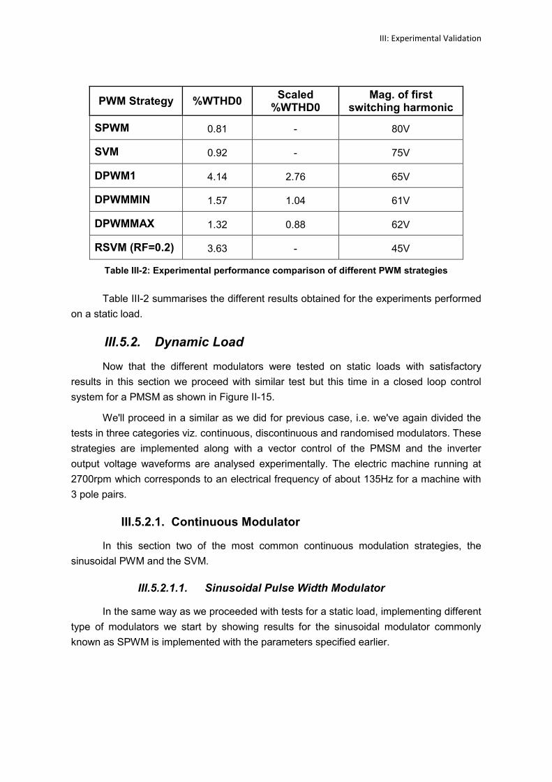
III: Experimental Validation
PWM Strategy %WTHD0Scaled%WTHD0
Mag. of firstswitching harmonic
SPWM 0.81 - 80V
SVM 0.92 - 75V
DPWM1 4.14 2.76 65V
DPWMMIN 1.57 1.04 61V
DPWMMAX 1.32 0.88 62V
RSVM (RF=0.2) 3.63 - 45V
Table III-2: Experimental performance comparison of different PWM strategies
Table III-2 summarises the different results obtained for the experiments performed
on a static load.
III.5.2. Dynamic Load
Now that the different modulators were tested on static loads with satisfactory
results in this section we proceed with similar test but this time in a closed loop control
system for a PMSM as shown in Figure II-15.
We'll proceed in a similar as we did for previous case, i.e. we've again divided the
tests in three categories viz. continuous, discontinuous and randomised modulators. These
strategies are implemented along with a vector control of the PMSM and the inverter
output voltage waveforms are analysed experimentally. The electric machine running at
2700rpm which corresponds to an electrical frequency of about 135Hz for a machine with
3 pole pairs.
III.5.2.1. Continuous Modulator
In this section two of the most common continuous modulation strategies, the
sinusoidal PWM and the SVM.
III.5.2.1.1. Sinusoidal Pulse Width Modulator
In the same way as we proceeded with tests for a static load, implementing different
type of modulators we start by showing results for the sinusoidal modulator commonly
known as SPWM is implemented with the parameters specified earlier.
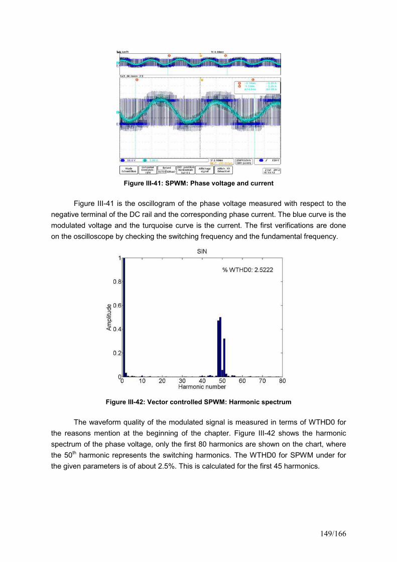
149/166
Figure III-41: SPWM: Phase voltage and current
Figure III-41 is the oscillogram of the phase voltage measured with respect to the
negative terminal of the DC rail and the corresponding phase current. The blue curve is the
modulated voltage and the turquoise curve is the current. The first verifications are done
on the oscilloscope by checking the switching frequency and the fundamental frequency.
Figure III-42: Vector controlled SPWM: Harmonic spectrum
The waveform quality of the modulated signal is measured in terms of WTHD0 for
the reasons mention at the beginning of the chapter. Figure III-42 shows the harmonic
spectrum of the phase voltage, only the first 80 harmonics are shown on the chart, where
the 50th harmonic represents the switching harmonics. The WTHD0 for SPWM under for
the given parameters is of about 2.5%. This is calculated for the first 45 harmonics.
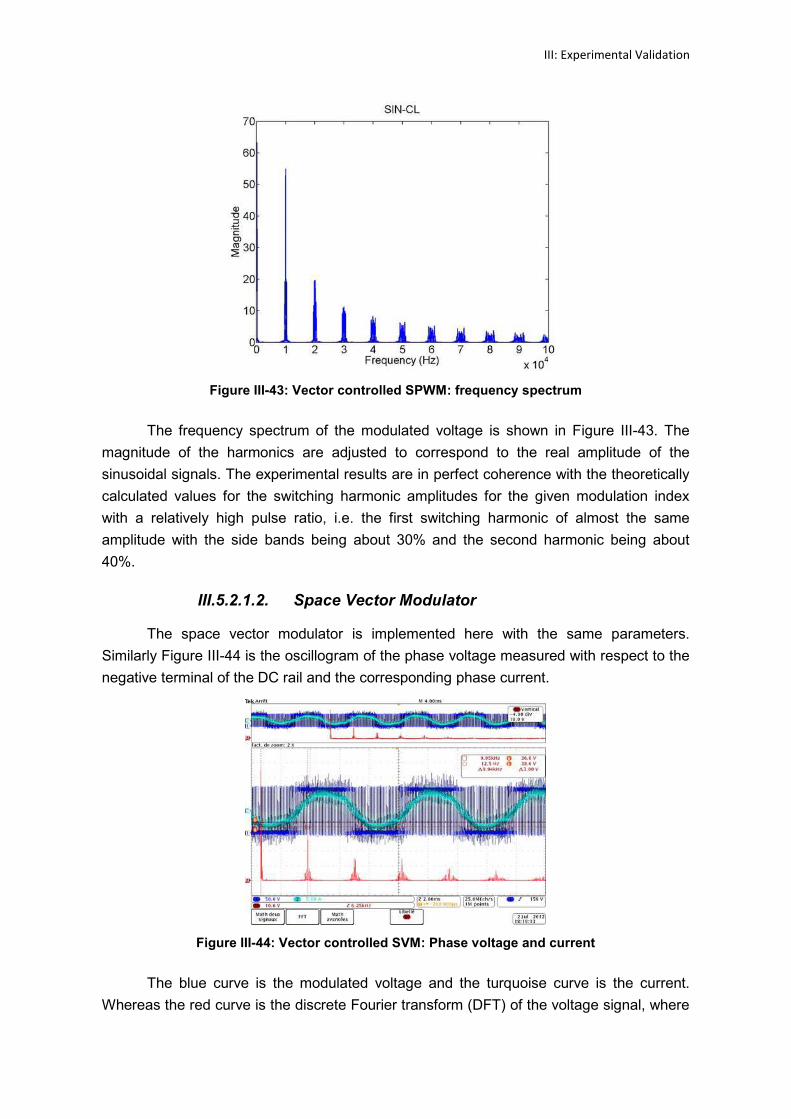
III: Experimental Validation
Figure III-43: Vector controlled SPWM: frequency spectrum
The frequency spectrum of the modulated voltage is shown in Figure III-43. The
magnitude of the harmonics are adjusted to correspond to the real amplitude of the
sinusoidal signals. The experimental results are in perfect coherence with the theoretically
calculated values for the switching harmonic amplitudes for the given modulation index
with a relatively high pulse ratio, i.e. the first switching harmonic of almost the same
amplitude with the side bands being about 30% and the second harmonic being about
40%.
III.5.2.1.2. Space Vector Modulator
The space vector modulator is implemented here with the same parameters.
Similarly Figure III-44 is the oscillogram of the phase voltage measured with respect to the
negative terminal of the DC rail and the corresponding phase current.
Figure III-44: Vector controlled SVM: Phase voltage and current
The blue curve is the modulated voltage and the turquoise curve is the current.
Whereas the red curve is the discrete Fourier transform (DFT) of the voltage signal, where
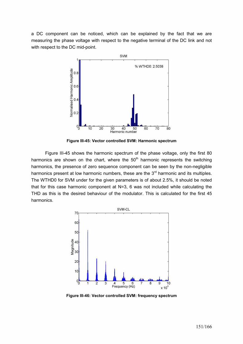
151/166
a DC component can be noticed, which can be explained by the fact that we are
measuring the phase voltage with respect to the negative terminal of the DC link and not
with respect to the DC mid-point.
Figure III-45: Vector controlled SVM: Harmonic spectrum
Figure III-45 shows the harmonic spectrum of the phase voltage, only the first 80
harmonics are shown on the chart, where the 50th harmonic represents the switching
harmonics, the presence of zero sequence component can be seen by the non-negligible
harmonics present at low harmonic numbers, these are the 3rd harmonic and its multiples.
The WTHD0 for SVM under for the given parameters is of about 2.5%, it should be noted
that for this case harmonic component at N=3, 6 was not included while calculating the
THD as this is the desired behaviour of the modulator. This is calculated for the first 45
harmonics.
Figure III-46: Vector controlled SVM: frequency spectrum

III: Experimental Validation
The frequency spectrum of the modulated voltage is shown in Figure III-46. The
magnitude of the harmonics are adjusted to correspond to the real amplitude of the
sinusoidal signals. Some low frequency components can be seen in the figure which again
are due to the presence of the zero sequence voltages.
III.5.2.2. Discontinuous modulator
In this section three discontinuous modulation strategies DPWMMIN and
DPWMMAX and EDSVM are implemented and analysed experimentally. Evolutive DSVM
is chosen in this case as we have a dynamic load, we can do the current tracking. Since
these types of modulators require a zero sequence voltage to be injected. In order
explicitly show the presence of these harmonics phase voltages are considered for the
harmonic and spectral analysis.
III.5.2.2.1. DPWMMIN & DPWMMAX
DPWMMIN and DPWMMAX as seen in section I.2.4.2.2 are two discontinuous
modulators which are similar to each other.
Figure III-47: Vector controlled DSVMMAX:Phase voltage and current
Figure III-48: Vector controlled DSVMMIN:Phase voltage and current
Figure III-47 and Figure III-48 are the oscillograms of the phase voltage measured
with respect to the negative terminal of the DC rail and the corresponding phase current for
DPWMMAX and DPWMMIN respectively. The discontinuities are clearly visible on the blue
curves which are the modulated voltage, the turquoise curves are the phase currents
which again remain sinusoidal. However higher current ripples, the current curve is a little
thicker which can be easily observed on the figures this again is due to the reduced
effective switching frequency.
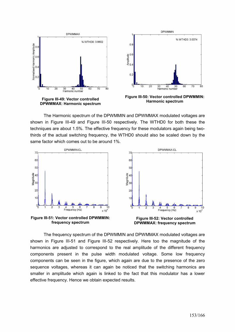
153/166
Figure III-49: Vector controlledDPWMMAX: Harmonic spectrum
Figure III-50: Vector controlled DPWMMIN:Harmonic spectrum
The Harmonic spectrum of the DPWMMIN and DPWMMAX modulated voltages are
shown in Figure III-49 and Figure III-50 respectively. The WTHD0 for both these the
techniques are about 1.5%. The effective frequency for these modulators again being two-
thirds of the actual switching frequency, the WTHD0 should also be scaled down by the
same factor which comes out to be around 1%.
Figure III-51: Vector controlled DPWMMIN:frequency spectrum
Figure III-52: Vector controlledDPWMMAX: frequency spectrum
The frequency spectrum of the DPWMMIN and DPWMMAX modulated voltages are
shown in Figure III-51 and Figure III-52 respectively. Here too the magnitude of the
harmonics are adjusted to correspond to the real amplitude of the different frequency
components present in the pulse width modulated voltage. Some low frequency
components can be seen in the figure, which again are due to the presence of the zero
sequence voltages, whereas it can again be noticed that the switching harmonics are
smaller in amplitude which again is linked to the fact that this modulator has a lower
effective frequency. Hence we obtain expected results.
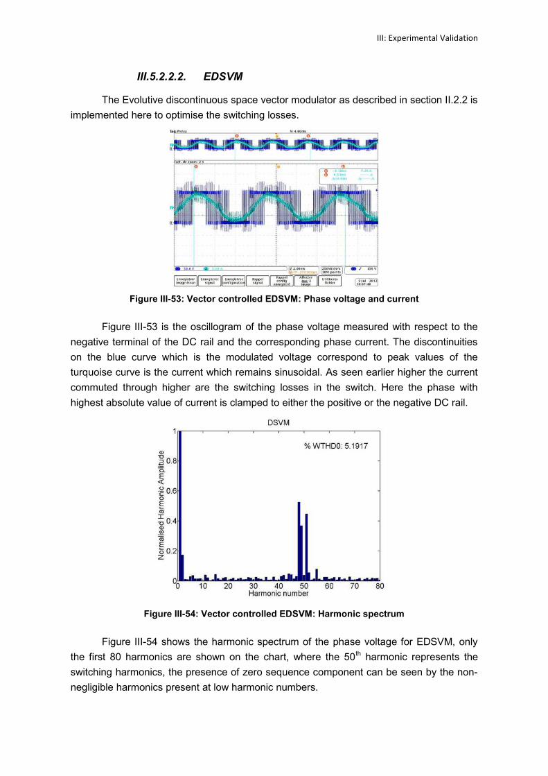
III: Experimental Validation
III.5.2.2.2. EDSVM
The Evolutive discontinuous space vector modulator as described in section II.2.2 is
implemented here to optimise the switching losses.
Figure III-53: Vector controlled EDSVM: Phase voltage and current
Figure III-53 is the oscillogram of the phase voltage measured with respect to the
negative terminal of the DC rail and the corresponding phase current. The discontinuities
on the blue curve which is the modulated voltage correspond to peak values of the
turquoise curve is the current which remains sinusoidal. As seen earlier higher the current
commuted through higher are the switching losses in the switch. Here the phase with
highest absolute value of current is clamped to either the positive or the negative DC rail.
Figure III-54: Vector controlled EDSVM: Harmonic spectrum
Figure III-54 shows the harmonic spectrum of the phase voltage for EDSVM, only
the first 80 harmonics are shown on the chart, where the 50th harmonic represents the
switching harmonics, the presence of zero sequence component can be seen by the non-
negligible harmonics present at low harmonic numbers.
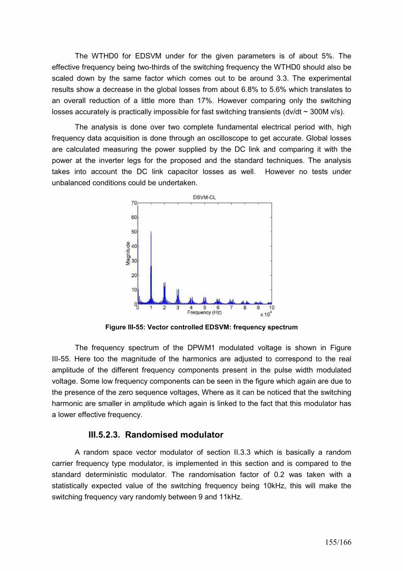
155/166
The WTHD0 for EDSVM under for the given parameters is of about 5%. The
effective frequency being two-thirds of the switching frequency the WTHD0 should also be
scaled down by the same factor which comes out to be around 3.3. The experimental
results show a decrease in the global losses from about 6.8% to 5.6% which translates to
an overall reduction of a little more than 17%. However comparing only the switching
losses accurately is practically impossible for fast switching transients (dv/dt ~ 300M v/s).
The analysis is done over two complete fundamental electrical period with, high
frequency data acquisition is done through an oscilloscope to get accurate. Global losses
are calculated measuring the power supplied by the DC link and comparing it with the
power at the inverter legs for the proposed and the standard techniques. The analysis
takes into account the DC link capacitor losses as well. However no tests under
unbalanced conditions could be undertaken.
Figure III-55: Vector controlled EDSVM: frequency spectrum
The frequency spectrum of the DPWM1 modulated voltage is shown in Figure
III-55. Here too the magnitude of the harmonics are adjusted to correspond to the real
amplitude of the different frequency components present in the pulse width modulated
voltage. Some low frequency components can be seen in the figure which again are due to
the presence of the zero sequence voltages, Where as it can be noticed that the switching
harmonic are smaller in amplitude which again is linked to the fact that this modulator has
a lower effective frequency.
III.5.2.3. Randomised modulator
A random space vector modulator of section II.3.3 which is basically a random
carrier frequency type modulator, is implemented in this section and is compared to the
standard deterministic modulator. The randomisation factor of 0.2 was taken with a
statistically expected value of the switching frequency being 10kHz, this will make the
switching frequency vary randomly between 9 and 11kHz.
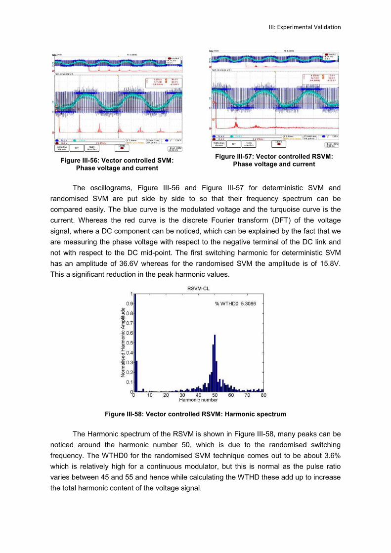
III: Experimental Validation
Figure III-56: Vector controlled SVM:Phase voltage and current
Figure III-57: Vector controlled RSVM:Phase voltage and current
The oscillograms, Figure III-56 and Figure III-57 for deterministic SVM and
randomised SVM are put side by side to so that their frequency spectrum can be
compared easily. The blue curve is the modulated voltage and the turquoise curve is the
current. Whereas the red curve is the discrete Fourier transform (DFT) of the voltage
signal, where a DC component can be noticed, which can be explained by the fact that we
are measuring the phase voltage with respect to the negative terminal of the DC link and
not with respect to the DC mid-point. The first switching harmonic for deterministic SVM
has an amplitude of 36.6V whereas for the randomised SVM the amplitude is of 15.8V.
This a significant reduction in the peak harmonic values.
Figure III-58: Vector controlled RSVM: Harmonic spectrum
The Harmonic spectrum of the RSVM is shown in Figure III-58, many peaks can be
noticed around the harmonic number 50, which is due to the randomised switching
frequency. The WTHD0 for the randomised SVM technique comes out to be about 3.6%
which is relatively high for a continuous modulator, but this is normal as the pulse ratio
varies between 45 and 55 and hence while calculating the WTHD these add up to increase
the total harmonic content of the voltage signal.
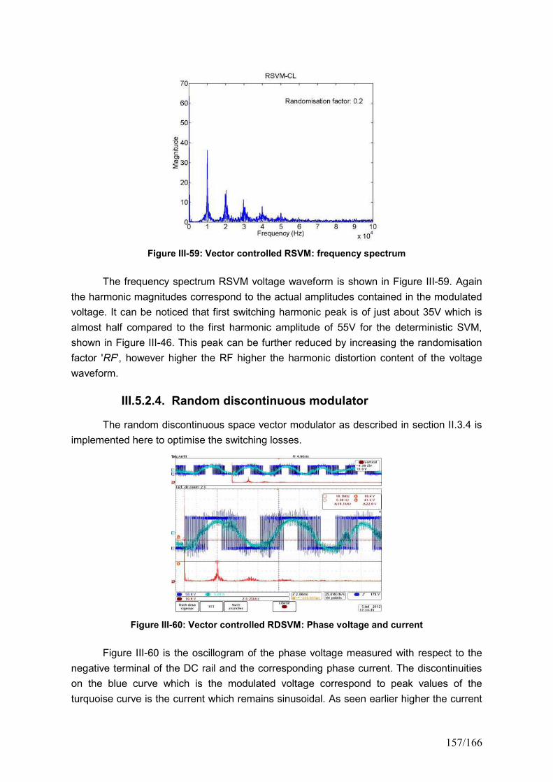
157/166
Figure III-59: Vector controlled RSVM: frequency spectrum
The frequency spectrum RSVM voltage waveform is shown in Figure III-59. Again
the harmonic magnitudes correspond to the actual amplitudes contained in the modulated
voltage. It can be noticed that first switching harmonic peak is of just about 35V which is
almost half compared to the first harmonic amplitude of 55V for the deterministic SVM,
shown in Figure III-46. This peak can be further reduced by increasing the randomisation
factor 'RF', however higher the RF higher the harmonic distortion content of the voltage
waveform.
III.5.2.4. Random discontinuous modulator
The random discontinuous space vector modulator as described in section II.3.4 is
implemented here to optimise the switching losses.
Figure III-60: Vector controlled RDSVM: Phase voltage and current
Figure III-60 is the oscillogram of the phase voltage measured with respect to the
negative terminal of the DC rail and the corresponding phase current. The discontinuities
on the blue curve which is the modulated voltage correspond to peak values of the
turquoise curve is the current which remains sinusoidal. As seen earlier higher the current
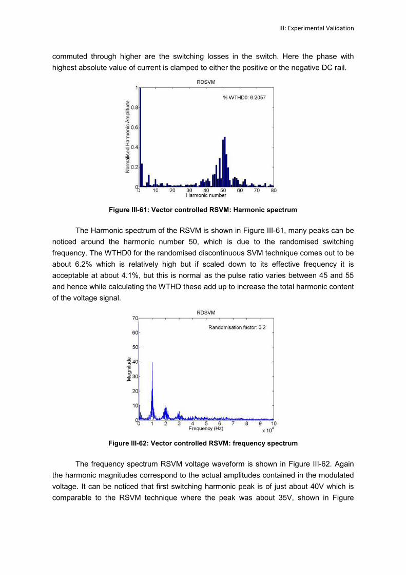
III: Experimental Validation
commuted through higher are the switching losses in the switch. Here the phase with
highest absolute value of current is clamped to either the positive or the negative DC rail.
Figure III-61: Vector controlled RSVM: Harmonic spectrum
The Harmonic spectrum of the RSVM is shown in Figure III-61, many peaks can be
noticed around the harmonic number 50, which is due to the randomised switching
frequency. The WTHD0 for the randomised discontinuous SVM technique comes out to be
about 6.2% which is relatively high but if scaled down to its effective frequency it is
acceptable at about 4.1%, but this is normal as the pulse ratio varies between 45 and 55
and hence while calculating the WTHD these add up to increase the total harmonic content
of the voltage signal.
Figure III-62: Vector controlled RSVM: frequency spectrum
The frequency spectrum RSVM voltage waveform is shown in Figure III-62. Again
the harmonic magnitudes correspond to the actual amplitudes contained in the modulated
voltage. It can be noticed that first switching harmonic peak is of just about 40V which is
comparable to the RSVM technique where the peak was about 35V, shown in Figure
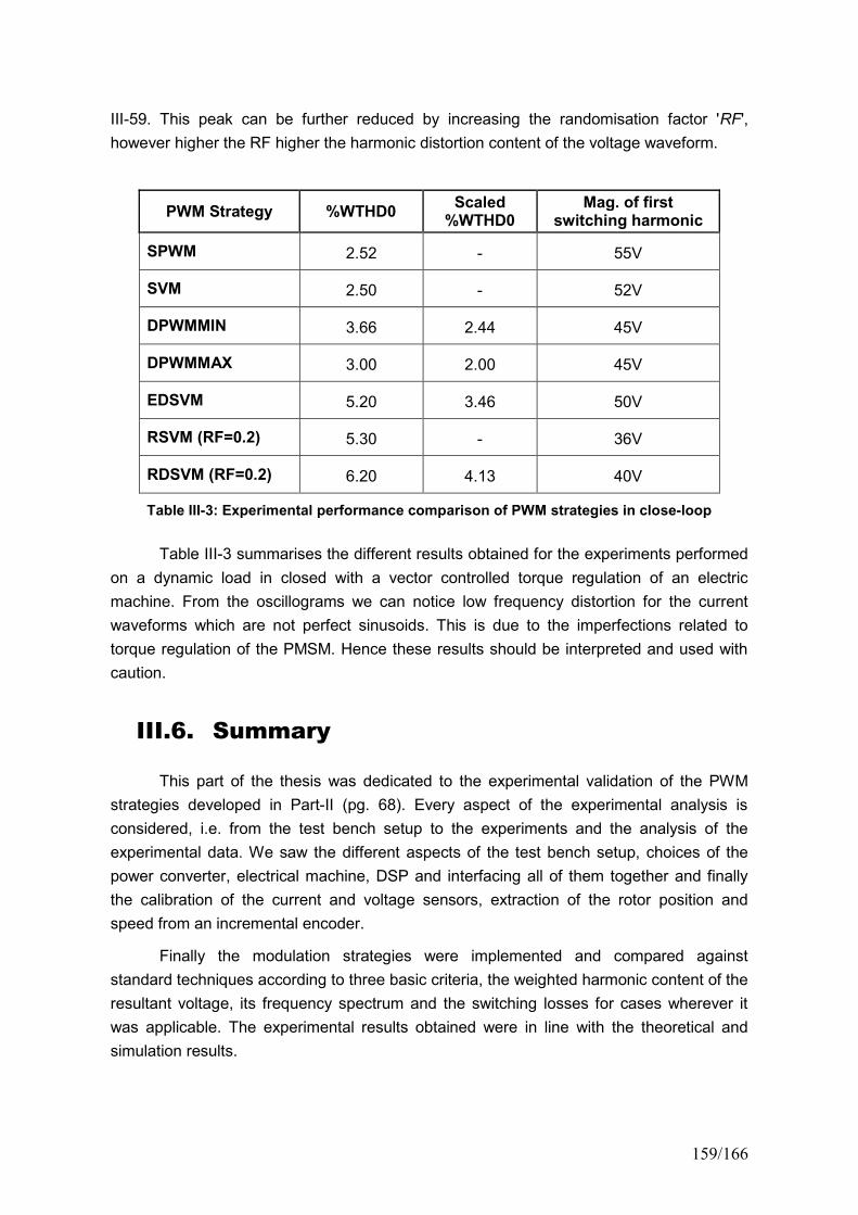
159/166
III-59. This peak can be further reduced by increasing the randomisation factor 'RF',
however higher the RF higher the harmonic distortion content of the voltage waveform.
PWM Strategy %WTHD0Scaled%WTHD0
Mag. of firstswitching harmonic
SPWM 2.52 - 55V
SVM 2.50 - 52V
DPWMMIN 3.66 2.44 45V
DPWMMAX 3.00 2.00 45V
EDSVM 5.20 3.46 50V
RSVM (RF=0.2) 5.30 - 36V
RDSVM (RF=0.2) 6.20 4.13 40V
Table III-3: Experimental performance comparison of PWM strategies in close-loop
Table III-3 summarises the different results obtained for the experiments performed
on a dynamic load in closed with a vector controlled torque regulation of an electric
machine. From the oscillograms we can notice low frequency distortion for the current
waveforms which are not perfect sinusoids. This is due to the imperfections related to
torque regulation of the PMSM. Hence these results should be interpreted and used with
caution.
III.6. Summary
This part of the thesis was dedicated to the experimental validation of the PWM
strategies developed in Part-II (pg. 68). Every aspect of the experimental analysis is
considered, i.e. from the test bench setup to the experiments and the analysis of the
experimental data. We saw the different aspects of the test bench setup, choices of the
power converter, electrical machine, DSP and interfacing all of them together and finally
the calibration of the current and voltage sensors, extraction of the rotor position and
speed from an incremental encoder.
Finally the modulation strategies were implemented and compared against
standard techniques according to three basic criteria, the weighted harmonic content of the
resultant voltage, its frequency spectrum and the switching losses for cases wherever it
was applicable. The experimental results obtained were in line with the theoretical and
simulation results.

PART IV
CONCLUSION & FUTUREWORK
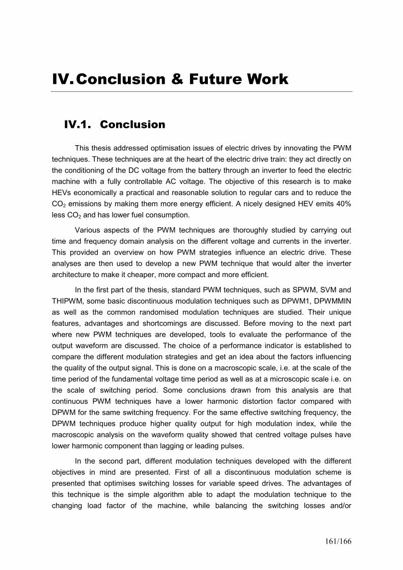
161/166
IV.Conclusion & Future Work
IV.1. Conclusion
This thesis addressed optimisation issues of electric drives by innovating the PWM
techniques. These techniques are at the heart of the electric drive train: they act directly on
the conditioning of the DC voltage from the battery through an inverter to feed the electric
machine with a fully controllable AC voltage. The objective of this research is to make
HEVs economically a practical and reasonable solution to regular cars and to reduce the
CO2 emissions by making them more energy efficient. A nicely designed HEV emits 40%
less CO2 and has lower fuel consumption.
Various aspects of the PWM techniques are thoroughly studied by carrying out
time and frequency domain analysis on the different voltage and currents in the inverter.
This provided an overview on how PWM strategies influence an electric drive. These
analyses are then used to develop a new PWM technique that would alter the inverter
architecture to make it cheaper, more compact and more efficient.
In the first part of the thesis, standard PWM techniques, such as SPWM, SVM and
THIPWM, some basic discontinuous modulation techniques such as DPWM1, DPWMMIN
as well as the common randomised modulation techniques are studied. Their unique
features, advantages and shortcomings are discussed. Before moving to the next part
where new PWM techniques are developed, tools to evaluate the performance of the
output waveform are discussed. The choice of a performance indicator is established to
compare the different modulation strategies and get an idea about the factors influencing
the quality of the output signal. This is done on a macroscopic scale, i.e. at the scale of the
time period of the fundamental voltage time period as well as at a microscopic scale i.e. on
the scale of switching period. Some conclusions drawn from this analysis are that
continuous PWM techniques have a lower harmonic distortion factor compared with
DPWM for the same switching frequency. For the same effective switching frequency, the
DPWM techniques produce higher quality output for high modulation index, while the
macroscopic analysis on the waveform quality showed that centred voltage pulses have
lower harmonic component than lagging or leading pulses.
In the second part, different modulation techniques developed with the different
objectives in mind are presented. First of all a discontinuous modulation scheme is
presented that optimises switching losses for variable speed drives. The advantages of
this technique is the simple algorithm able to adapt the modulation technique to the
changing load factor of the machine, while balancing the switching losses and/or

IV:Conclusion
temperature difference, if any, between the different inverter legs. This not only increases
the efficiency of the inverter, leading to a smaller heat sink and hence reduced volume but
also ensures a longer life. Owing to its intelligence, this modulation technique can
introduce non-uniformity in terms of the switching patterns among the three phases. This
lets the weakest phase idle longer than the other two phases, extending the life cycle of
the inverter. A random carrier frequency modulator is proposed and the choice is
theoretically justified. Frequency domain analysis shows considerable reduction in the
switching harmonics. This will lead to reduced EM emissions and hence lower possibility of
these high frequency voltages interfering with other electronic components in the vicinity.
However no emission measurement could be undertaken due to lack of time and
resources.
A technique where phase currents can be deduced by measuring only the inverter
input current is also presented. This technique is made applicable through out the hexagon
using pulse placement techniques. This technique avoids the need of two phase current
sensors hence reducing the cost of the inverter module. The last technique presented in
this part is the reduction of the inverter input current ripple. This is done by using non-
adjacent active vectors. From the implementation point of view, these techniques are a
little complicated and require the right set of vectors to be used. The proposed technique
can reduce the RMS value of the inverter input current ripple by 20%. This decrease in the
ripple component means a smaller DC-link capacitor in volume by the same factor.
However the use of non-adjacent vectors decreases the waveform quality of the output
voltage. These techniques could not be experimentally verified due to the architecture of
the power module, where the current sensor is place before the DC-Link capacitor and
hence gives filtered or average values.
After laying down the theoretical foundations that were tested through computer
simulations, the discontinuous and randomised techniques are experimentally tested with
PMSM as the load. A test platform was developed for this purpose. The basic work done
was to interface the DSP with the IGBT module while conditioning the signals. One of the
main aspects of the test bench is that it supports rapid prototyping through Simulink. One
of the requirements relates to the controllability of the fundamental component of the
voltage and its quality and the other is its harmonic spectrum. The proposed techniques
are successfully implemented. The results obtained are very satisfactory. Reduction of
inverter losses for the proposed discontinuous modulator and harmonic dithering for the
randomised modulator were confirmed experimentally.

163/166
IV.2. Suggestions for future work
The field of science knows no limits; one can work all one's life in a specific domain
and discover new things everyday, the possibilities of improving and to reaching perfection
never end. A Ph.D. offers a limited time to do research and document it; I was given three
years. In this thesis I've presented my finding during these past three years as a Ph.D.
candidate. The field of PWM is vast, a lot has been done and still remain to be
accomplished. I hope I will be able to work some more on some of the issues.
The objective of my thesis here was to reduce the cost, volume and weight of
electric drives through innovative PWM techniques. Results were shown that have a direct
influence on these aforementioned parameters. EMI measurements have to be carried out
to quantify the real gain in terms of electromagnetic emissions. This would help the
dimensioning of the passive filters to meet the EMI standards for the new techniques which
can then be compared against EMI filters required for standard deterministic PWM
techniques. Similarly the heat sink needs to be re-dimensioned according to the reduced
losses for the discontinuous modulator.
Experimental validation of the technique proposed to reduce the inverter input
current ripple content has to be done, followed by re-dimensioning of the DC-link
capacitors. A major task that should be looked into is the fusion of these techniques, this
sure is a challenge, when there is more than one parameter to minimize. This will turn into
an optimisation problem with a rather complex cost function. Only after performing these
tasks can the final impact on the cost, volume and weight of the electric drive be
calculated.

REFERENCE
[1] Thomas B Fischer, "Towards a better consideration of climate change and greenhouse gas emissiontargets in transport and spatial/ land use policies, plans and programmes", 2001
[2] The Environmental Impact of the Car, Greenpeace International, 1991. ISBN 871532 361.[3] CO2 emissions from fuel combustion – Highlights, 2011 Edition, International Energy Agency, 2011.[4] Ali Emadi, "Handbook of Automotive and Power Electronics and Motor Drives" 2005 CRC Press, Taylor
and Francis Group.[5] M. Ehsani et al. “Toward a Sustainable Transportation without Sacrifice of Range, Performance, or Air
Quality: The ELPH Car Concept,” FISITA, International Federation of Automotive Engineering Society,Automotive Congress, September 27–October 1, 1998, Paris, France.
[6] M. Ehsani, K.L. Butler, Y. Gao, and K.M. Rahman, “Next Generation Passenger Cars with Better Range,Performance, and Emissions: The ELPH Car Concept”, Horizon in Engineering Symposium, TexasA&M University–Engineering Program Office, College Station, TX, September 23–25, 1998.
[7] C.C. Chan and K.T. Chau, Modern Electric Vehicle Technology, Oxford University Press, Inc., NewYork, 2001.
[8] Iqbal Husain, "Electric and hybrid Vehicles, Design and Fundamentals" 2011 CRC Press, Taylor andFrancis Group.
[9] Matthias Felden et al. "Electric Vehicle Drive Trains: From the Specification Sheet to the Drive-TrainConcept", 14th International Power Electronics and Motion Control Conference, EPE-PEMC 2010.
[10]H. L. Huy, "Comparison of Field-Oriented Control and Direct Torque Control for Induction MotorDrives", IEEE Industry Applications Conference 1999.
[11]R. Redl et al. "Electromagnetic environmental impact of power electronics equipment", IEEEProceedings, June 2001.
[12] F. Blaabjerg et al. "An extended model of power losses in hard-switched IGBT-inverters", IEEE IndustryApplications Conference, 1996.
[13] J. M. Erdman et al., "Effect of PWM inverters on AC motor bearing currents and shaft voltages", IEEEtransactions on Industry Applications, 1996.
[14]W. C. Lo et al. "Acoustic noise radiated by PWM-controlled induction machine drives", IEEETransactions on Industrial Electronics, 2000.
[15]B. D. Bedford and R. G. Hoft, "Principles of Inverter Circuits", John Wiley &Sons, New York, 1964.[16]D. Grahame Holmes, T. A. Lipo ""Pusle Width Modulation for Power Converters", IEEE series on power
engineering, John Wiley and Sons, 2003.[17] J. Holtz, “Pulse Width Modulation for Electronic Power Conversion,” pp. 1194–1214, Proceeding of the
IEEE , Vol. 82, Issue 8.[18]K. Zhou et al. "Relationship between space-vector modulation and three-phase carrier-based PWM: a
comprehensive analysis", IEEE Transactions on Industrial Electronics, 2002.[19]Ahmet M. Hava, Russel J. Kerkman, Thomas A. Lipo “A High-Performance Generalized Discontinuous
PWM Algorithm", IEEE Transactions On Industry Applications, VOL. 34, NO. 5, September/October1998.
[20] J. W. Kolar, H. Ertl, and F. C. Zach. \Minimization of the harmonic RMS content of the mains current ofa PWM converter system based on the solution of an extreme value problem". In ICHPC Conf. Records,pages 234-243, Budapest,Hungary, 1990.
[21]S. Mahdavi, J. Agah, “Application of Random PWM Technique for Reducing the Conducted
Electromagnetic Emissions in Active Filters”, Industrial Electronics, IEEE Transactions, vol. 54 pp.2333 - 2343, Aug. 2007.
[22]V. Blasko, M. Bech, “A new hybrid random pulse width modulator for industrial drives", Applied PowerElectronics Conference and Exposition, IEEE 2000, New Orleans, LA, USA. vol. 2 pp.932-938, 2000.
165/166
[23]R. L. Kirlin et al., "Power spectra of a PWM inverter with randomized pulse position", IEEETransactions on Power Electronics, 1994.
[24]K. El Khamlichi Drissi, P.C.K. Luk, B. Wang and J. Fontaine, “A Novel Dual-Randomization PWMScheme for Power Converters”, 34th IEEE Power Electronics Specialists Conference (PESC), vol. 2, pp.480-484, 15-19 June 2003, Acapulco, Mexico.
[25]N. Boudjerda, M. Melit, B. Nekhoul, K. El Khamlichi Drissi and K. Kerroum, “Spread spectrum in DC-DC full bridge voltage converter by a dual randomized PWM scheme", Electromagnetic Compatibility -EMC Europe, 2008, Hamburg, pp. 181-186, September 2008.
[26]Michael M. Bech, “Analysis of Random Pulse-Width Modulation Techniques for Power Electronic
Converters", PhD Thesis submitted to the Faculty of Engineering & Science at Aalborg University,pp.22-26, August 2002.
[27]K. El Khamlichi Drissi, P.C.K. Luk and B. Wang, “Effects of symmetric distribution laws on spectralpower density in randomized PWM ", Power Electronics Letters, IEEE, vol. 1 pp.41-44, June 2003.
[28]Hamid Khan, E.H. Miliani, Khalil El Khamlichi Drissi, "Altered PWM for DC link current translation tophase currents for electric drives", 7th International Power Electronics and Motion Control ConferenceIPEMC - ECCE Asia 2012, June 2-5, Harbin, China 2012.
[29]S. R. Bowes et al., "The relationship between space-vector modulation and regular-sampled PWM" IEEETransactions on Industrial Electronics, 1997.
[30]Hamid Khan, E.H. Miliani, Khalil El Khamlichi Drissi, "Discontinuous Random Space VectorModulation for Electric Drives: A Digital Approach", IEEE Transactions On Power Electronics, VOL.27, NO. 12, December 2012.
[31]Hamid Khan, E.H. Miliani, Khalil El Khamlichi Drissi, "Evolutive Discontinuous SVM for Variable
Speed Electric Drive", Power Electronics and Adjustable Speed Drives EPE - ECCE Europe 2011,Birmingham, UK, 30 August-1 September 2011.
[32]Antônio S. de Oliveira Jr., Edison R. da Silva, “Random Space Vector Modulation for 3-Level PowerInverters and Induction Motor Drives Current Control ", Power Electronics Specialists Conference, vol.36 pp.987-993, June 2005.
[33]M. Zigliotto, A. M. Trzynadlowski, “Effective Random Space Vector Modulation for EMI Reduction inLow-Cost PWM Inverters", Power Electronics and Variable Speed Drives 1998, IEEE, pp.163-168, Sep1998.
[34]S. Bolognani, R. Conton, “Experimental Analysis of the EMI Reduction in PWM Inverters Using RandomSpace vector Modulation", Industrial Electronics, IEEE, 1996, vol. 1 pp. 482 - 487, Jun 1996.
[35]Yen-Shin Lai, “Random space vector modulation technique for high switching frequency inverter control", Electronics Letters 1997, IEEE, vol. A4 pp.108-117, September 2008.
[36]Hamid Khan, Youssef Touzani, Khalil El Khamlichi Drissi, "Random Space Vector Modulation for
Electric Drives: A Digital Approach" 14th International Power Electronics and Motion ControlConference, EPE-PEMC 2010.
[37]Hamid Khan, E.H. Miliani, Khalil El Khamlichi Drissi, "Random Discontinuous Space Vector
Modulation for Variable Speed Drives", International Conference on Industrial Technology, ICIT 2012,Athens Grece 2012.
[38]Hamid Khan, E.H. Miliani, Khalil El Khamlichi Drissi, "Novel Technique to Reduce Leakage Currentand Commutation Losses in Electric Drives" International Conference on Power Electronics ICPE -ECCE Asia 2011, Jeju, Korea, 30th May – 3rd June 2011.
[39]Andrzej M. Trzynadlowski, Stanislaw Legowski “Minimum-Loss Vector PWM Strategy for Three-phaseInverters ", Electronics Letters 1997, IEEE, vol. A4 pp.108-117, September 2008.
[40]Zare, Firuz, "EMI in modern AC motor drive systems", IEEE EMC Society, Newsletters, 2009, pp. 53-58.
[41]N.Idir, Y.Weens, M.Moreau, J.J.Franchaud, “High-Frequency Behaviour Models of AC Motors” IEEETransactions on Magnetics, Volume 45, Issue 1, Part 1, pp.133 - 138, Jan. 2009.
[42]Sabine Marksell, "EMC Aspects of PWM Controlled Loads in Vehicles" PhD thesis. Department ofIndustrial Electrical Engineering and Automation, LUND University, 2004.
[43]S. K. Park and K. W. Miller, "Random number generators: Good ones are hard to find", Communicationsof the ACM, 31 ,1988, pp. 1192-1201.
[44]Hong Zhang and Qihua Zhao, "Switching Harmonics in a Three-Phase PWM Inverter", SAE TechnicalPaper Series, Power Systems Conference New Orleans, Louisiana November 7-9, 2006.
[45]G. Marsaglia and A. Zaman, "A new class of random number generators", Annals of Applied Probability,3, 1991, pp. 462-480.
[46]H. Kim and T. M. Jahns, “Phase current reconstruction for AC motor drives using a DC link singlecurrent sensor and measurement voltage vectors,” IEEE Trans. Power Electron., vol. 21, no. 5, pp. 1413–1419, Sep. 2006.
[47] Jung-Ik Ha, "Current Prediction in Vector-Controlled PWM Inverters Using Single DC-Link CurrentSensor," IEEE Trans. Industrial Electron., vol. 57, no. 2, pp. 716-726, Feb. 2010
[48] J. K. Pedersen and F. Blaabjerg, “An ideal PWM–VSI inverter using only one current sensor in the dc-link,” in Proc. PEVD’94, 1994, pp. 458–464.
[49]M. Riese, “Phase current reconstruction of a three-phase voltage source inverter-fed drive using sensor inthe dc-link,” in Proc. PCIM’96, 1996, pp. 95–101.
[50]F. Blaabjerg, J. K. Pedersen, U. Jaeger, and P. Thoegersen, “Single current sensor technique in the DClink of three-phase PWM-VS inverters: A review and a novel solution,” IEEE Trans. Ind. Appl., vol. 33,no. 5,pp. 1241–1253, Sep. 1997.
[51]F. Blaabjerg and J. K. Pedersen, “A new low-cost fully fault protected PWM–VSI inverter with truephase-current information,” in Proc. IPEC’95, 1995, vol. 2, pp. 984–991.
[52]Yen-Shin Lai, Po-Sheng Chen, Hsiang-Kuo Lee, J Chou, "Optimal Common-Mode Voltage ReductionPWM Technique for Inverter Control With Consideration of the Dead-Time Effects—Part II:Applications to IM Drives With Diode Front End", IEEE Trans. Ind. Appl., vol. 40, no. 6,pp. 1613 -1620, Nov.-Dec. 2004.
[53]P.A. Dahono, Y. Sato, T. Kataoka, “Analysis and minimization of Ripple components of input currentand voltage of PWM inverters”, IEEE Trans. on Ind. App., vol. 32, No.4, July/August 1996.
[54] J.W. Kolar, H. Ertl, F.C. Zach, “Calculation of the passive and active component stress of three phasePWM converter systems with high pulse rate,” EPE 89, vol. 3, pp. 1303–1311, 1989.
[55] J. Hobraiche, J. P. Vilain, P. Marcet, N. Patin, "A new PWM strategy to reduce the inverter Input currentripples", IEEE Trans. on Power Electronics, vol. 24, No.1, January 2009.