Optics and Nonlinear Buckling ARTICLE Mechanics in...
8
GAO ET AL . VOL. 9 ’ NO. 6 ’ 5968–5975 ’ 2015 www.acsnano.org 5968 April 23, 2015 C 2015 American Chemical Society Optics and Nonlinear Buckling Mechanics in Large-Area, Highly Stretchable Arrays of Plasmonic Nanostructures Li Gao, †,‡,0 Yihui Zhang, §,^,0 Hui Zhang, ) ,0 Sage Doshay, [,0 Xu Xie, † Hongying Luo, §,r Deesha Shah, † Yan Shi, §,z Siyi Xu, † Hui Fang, † Jonathan A. Fan, # Peter Nordlander, ) ,£ Yonggang Huang, * ,§ and John A. Rogers * ,† † Departments of Materials Science and Engineering, Beckman Institute, and Frederick Seitz Materials Research Laboratory, University of Illinois at UrbanaChampaign, Urbana, Illinois 61801, United States, ‡ School of Electronic and Optical Engineering, Nanjing University of Science and Technology, Nanjing 210094, China, § Department of Mechanical Engineering and Department of Civil and Environmental Engineering, Center for Engineering and Health, and Skin Disease Research Center, Northwestern University, Evanston, Illinois 60208, United States, ^ Center for Mechanics and Materials, Tsinghua University, Beijing 100084, China, ) Department of Electrical and Computer Engineering and Material Science and Nanoengineering and £ Department of Physics and Astronomy, Rice University, Houston, Texas 77251, United States, # Department of Electrical Engineering and [ Department of Applied Physics, Stanford University, Stanford, California 94305, United States, r School of Aerospace Engineering and Applied Mechanics, Tongji University, Shanghai 200092, China, and z State Key Laboratory of Mechanics and Control of Mechanical Structures, Nanjing University of Aeronautics and Astronautics, Nanjing 210016, China. 0 L. Gao, Y. Zhang, H. Zhang, and S. Doshay contributed equally. R ecent research demonstrates that care- fully designed combinations of hard electronic nanomaterials with soft elas- tomers can, in optimized designs, yield high- performance integrated circuits with linear elastic responses to large strain deforma- tions. 16 These systems are of interest partly due to their application in advanced biome- dical devices that laminate on the curved, temporally dynamic surfaces of the human body, in ways that would be impossible with traditional electronics technologies. 7,8 Similar concepts appear to have utility in the inte- gration of optical nanomaterials and elasto- mers for unusual classes of metamaterials and plasmonic structures with options in mechanical tuning of the key properties. Recent work highlights initial examples of this type, including split ring resonators 9 and nanoantennas, 10 typically formed by electron beam lithography and then physically trans- ferred to elastomers, or by nanostencil litho- graphy to yield small devices (<0.01 mm 2 ) with modest levels of elastic deformation (∼10% and 21%, respectively), where linear mechanics dominate the responses. Pro- grammable soft lithography 11 allows large- scale nanoparticle arrays with variable den- sity tuned by stretching or heating using the methods of solvent-assisted nanoscale embossing. Here we report the use of ad- vanced transfer techniques 12 to realize * Address correspondence to [email protected], [email protected]. Received for review February 1, 2015 and accepted April 23, 2015. Published online 10.1021/acsnano.5b00716 ABSTRACT Large-scale, dense arrays of plasmonic nanodisks on low-modulus, high-elongation elastomeric substrates represent a class of tunable optical systems, with reversible ability to shift key optical resonances over a range of nearly 600 nm at near-infrared wavelengths. At the most extreme levels of mechanical deformation (strains >100%), nonlinear buckling processes transform initially planar arrays into three-dimensional configurations, in which the nanodisks rotate out of the plane to form linear arrays with “wavy” geometries. Analytical, finite-element, and finite-difference time-domain models capture not only the physics of these buckling processes, including all of the observed modes, but also the quantitative effects of these deformations on the plasmonic responses. The results have relevance to mechanically tunable optical systems, particularly to soft optical sensors that integrate on or in the human body. KEYWORDS: large-area nanodisk array . stretchable plasmonics . wide-band tunability . nanoscale buckling ARTICLE
Transcript of Optics and Nonlinear Buckling ARTICLE Mechanics in...

GAO ET AL . VOL. 9 ’ NO. 6 ’ 5968–5975 ’ 2015
www.acsnano.org
5968
April 23, 2015
C 2015 American Chemical Society
Optics and Nonlinear BucklingMechanics in Large-Area, HighlyStretchable Arrays of PlasmonicNanostructuresLi Gao,†,‡,0 Yihui Zhang,§,^,0 Hui Zhang, ),0 Sage Doshay,[,0 Xu Xie,† Hongying Luo,§,r Deesha Shah,†
Yan Shi,§,z Siyi Xu,† Hui Fang,† Jonathan A. Fan,# Peter Nordlander, ),£ Yonggang Huang,*,§ and
John A. Rogers*,†
†Departments of Materials Science and Engineering, Beckman Institute, and Frederick Seitz Materials Research Laboratory, University of Illinois atUrbana�Champaign, Urbana, Illinois 61801, United States, ‡School of Electronic and Optical Engineering, Nanjing University of Science and Technology,Nanjing 210094, China, §Department of Mechanical Engineering and Department of Civil and Environmental Engineering, Center for Engineering and Health,and Skin Disease Research Center, Northwestern University, Evanston, Illinois 60208, United States, ^Center for Mechanics and Materials, Tsinghua University,Beijing 100084, China, )Department of Electrical and Computer Engineering and Material Science and Nanoengineering and £Department of Physics and Astronomy,Rice University, Houston, Texas 77251, United States, #Department of Electrical Engineering and [Department of Applied Physics, Stanford University, Stanford,California 94305, United States,rSchool of Aerospace Engineering and Applied Mechanics, Tongji University, Shanghai 200092, China, and zState Key Laboratory ofMechanics and Control of Mechanical Structures, Nanjing University of Aeronautics and Astronautics, Nanjing 210016, China. 0L. Gao, Y. Zhang, H. Zhang, andS. Doshay contributed equally.
Recent researchdemonstrates that care-fully designed combinations of hardelectronic nanomaterialswith soft elas-
tomers can, in optimized designs, yield high-performance integrated circuits with linearelastic responses to large strain deforma-tions.1�6 These systems are of interest partlydue to their application in advanced biome-dical devices that laminate on the curved,temporally dynamic surfaces of the humanbody, in ways that would be impossible withtraditional electronics technologies.7,8 Similarconcepts appear to have utility in the inte-gration of optical nanomaterials and elasto-mers for unusual classes of metamaterialsand plasmonic structures with options in
mechanical tuning of the key properties.Recentwork highlights initial examples of thistype, including split ring resonators9 andnanoantennas,10 typically formed by electronbeam lithography and then physically trans-ferred to elastomers, or by nanostencil litho-graphy to yield small devices (<0.01 mm2)with modest levels of elastic deformation(∼10% and 21%, respectively), where linearmechanics dominate the responses. Pro-grammable soft lithography11 allows large-scale nanoparticle arrays with variable den-sity tuned by stretching or heating using themethods of solvent-assisted nanoscaleembossing. Here we report the use of ad-vanced transfer techniques12 to realize
* Address correspondence [email protected],[email protected].
Received for review February 1, 2015and accepted April 23, 2015.
Published online10.1021/acsnano.5b00716
ABSTRACT Large-scale, dense arrays of plasmonic nanodisks on low-modulus,
high-elongation elastomeric substrates represent a class of tunable optical
systems, with reversible ability to shift key optical resonances over a range of
nearly 600 nm at near-infrared wavelengths. At the most extreme levels of
mechanical deformation (strains >100%), nonlinear buckling processes transform
initially planar arrays into three-dimensional configurations, in which the
nanodisks rotate out of the plane to form linear arrays with “wavy” geometries.
Analytical, finite-element, and finite-difference time-domain models capture not
only the physics of these buckling processes, including all of the observed modes,
but also the quantitative effects of these deformations on the plasmonic responses. The results have relevance to mechanically tunable optical systems,
particularly to soft optical sensors that integrate on or in the human body.
KEYWORDS: large-area nanodisk array . stretchable plasmonics . wide-band tunability . nanoscale buckling
ARTIC
LE

GAO ET AL . VOL. 9 ’ NO. 6 ’ 5968–5975 ’ 2015
www.acsnano.org
5969
large-scale arrays of plasmonic nanodisks on elastomermaterials that can accommodate extremely high levelsof strain (∼100%). The results yield nearly defect-freesamples with practical sizes (several square centi-meters) and the ability to tune plasmonic resonancesover an exceptionally wide range, i.e., nearly 600 nm.Detailed studies of themechanics of uniaxial stretchingreveal not only the expected linear variations in thespacings between nanodisks, including Poisson ef-fects, but also nonlinear buckling that occurs abovea well-defined critical strain. This buckling transformsthe planar arrays into three-dimensional, noncoplanarlayouts, in quantitative agreement with semianalyticaltheory andfinite-element analysis. Experimentalmeasure-ments of normal-incidence optical transmission throughthese structures, along with corresponding finite-elementand finite-difference time-domain (FDTD) simulations,demonstrate the influence of these linear and nonlinearmechanical deformations on the optical properties.
RESULTS
The fabrication process (Figure S1a) involves transferprinting of multimaterial stacks deposited on siliconstamps that present square arrays of cylindrical postson their surfaces (period, P = 300 nm; diameter, D =200 nm; height, H = 300 nm). A conformal, ultrathinlayer (∼10 nm) of a fluoropolymer minimizes thestrength of adhesion to the silicon, thereby facilitatingtransfer. A representative stack (i.e., the ink) (Figure S1b)consists of 40 nm of gold as the functional plasmonicmaterial, with 5 nmof titaniumas an adhesion promoterto a top coating of 40 nm of silicon dioxide. The disks ofAu that form on the raised surfaces of the stamp havediameters of∼220 nm (∼200 nm from the silicon postsand an additional 20 nm from the fluoropolymer). Thediameters of the SiO2 disks on top are∼250 nm, due toeffects of slight angular growth during deposition.13
Contact against a soft silicone substrate (thickness∼300 μm) followed by mild heating promotes conden-sation reactions between surface �OH groups onthe SiO2 and the silicone, thereby creating strongbonds.Removing the stamp leaves the entire array of Au/Ti/SiO2 nanodisks well adhered to the surface of thesilicone, with exceptionally high yields (Figure S1c). Thissame procedure can be used with many other typesof plasmonic metals, as shown in Figure 1a�c for thecases of gold, silver, and aluminum. The colors ariseprincipally from plasmonic effects. Figure 1d,e show thegold sample in a tilted view and in a bent configura-tion to illustrate the uniformity in the color and themechanical compliance. These systems offer extremelyhigh levels of strechability, where the strains (applieduniaxially) can exceed ∼100% before fracture, as illu-strated in Figure 1f. Of particular interest here are thelarge-scale, 3D buckling structures that spontaneouslyappear above a certain critical level of uniaxial strain.Figure 1g,h present colorized (nanodisks, gold; silicone,
gray) scanning electron microscope (SEM) images(45� tilted view) that compare the arrays at zero appliedstrain to those at a strain of 107%. The latter reveals the3D geometry that spontaneously results from buckling.Cartoons based on calculations of finite-element ana-lyses (FEA) described subsequently appear in Figure 1i,j.Figure 2a provides additional detail on this strain-
induced geometry transformation. Here, SEM images(45� tilted view) reveal the changes in a given region ofthe sample (four rows by seven columns) for increasinglevels of uniaxial strain applied along the y direction.The gaps between the nanodisks decrease in the x
direction due to the Poisson effect. When the strainreaches a critical value, the spacings between the SiO2
section of the nanodisks in the x direction decrease tozero. Further stretching initiates nonlinear bucklinginstabilities that release the strain energy. This beha-vior appears clearly for the case of 56% strain, whereshort-range ordered waves that consist of five nano-disks in a period are dominant. This structure persistsbutwith increasing levels of out-of-plane displacementat strains of 72%, 89%, and 107%. Such behaviors canbe captured using FEA simulations (SupplementaryNote 1) and semianalytical methods (SupplementaryNote 2) as shown in Figure 2b,c. These approximatemodels appear schematically in Figure S2. In the non-buckling regime, the nanodisks themselves undergonegligible deformation, as evidenced by the experi-mental images and the FEA results (for applied strainεappl < 40%) in Figure 2. This response follows becausethe nanodisks are constructed of materials with muchhighermoduli than the silicone. Changes in the spacingsbetween the nanodisks in this non-buckling regime canbe captured using analytical models (SupplementaryNote 2), consistent with FEA results (Figure S2c) for allcases examined. The critical strain for the onset ofbuckling can be solved analytically (SupplementaryNote 2) by setting the nanodisk spacing along thetransverse direction to zero. Beyond the critical strain,the buckled configuration is more energetically favor-able compared to the nonbuckled one. In this regime, asemianalytical postbuckling model (SupplementaryNote 2 and Figure S3) can be formulated by adoptingbuckling modes observed in experiment, similar toapproaches used previously to describe buckling inthin films.4 FEA and semianalytical results are consis-tent with experiment at all strain levels (Figure S4).Figure 2d shows the results of atomic forcemicroscope(AFM) measurements of surface relief for a sampleat 72% strain, with comparisons to FEA results inFigure 2e. The height profile along line 1 in Figure 2dindicates an average wave amplitude of ∼163 nm,which agrees well with FEA prediction (∼174 nm) inFigure 2e. Over a 6 μm distance, both FEA resultsand experiment show approximately 6 periods.The profiles along line 2 in Figure 2d and e haveamplitudes of ∼100 nm, with 14.5 periods over an
ARTIC
LE

GAO ET AL . VOL. 9 ’ NO. 6 ’ 5968–5975 ’ 2015
www.acsnano.org
5970
8 μm distance, in agreement with FEA (∼100 nmand 15 periods), where ∼100 nm corresponds to themultilayer thickness of the nanodisks (∼85 nm). Suchbuckling behavior is quite different from that ofcontinuous ribbons/films on a silicone substrate.To compare these two systems, we studied a SiO2
ribbon of the same total thickness (∼85 nm) attachedto the top of the same silicone substrate. A direct
comparison of the buckling configurations appearsin Figure S5 for various levels of applied strain.The critical strain to trigger buckling in the contin-uous ribbons is typically much smaller than 1%,14
which is much less than that (∼44% in this case) fordiscrete nanodisks. The buckling configuration ofthe nanodisk system, although still in a wavy form,has characteristic wavelengths and amplitudes that
Figure 1. Arrays of plasmonic nanodisks with spacings and three-dimensional layouts that can be reversibly andcontinuously adjusted by mechanical stretching of a transparent elastomer support with high elastic elongation. (a) Opticalimage of a sample that consists of gold nanodisks. (b) Optical image of a sample that consists of silver nanodisks. (c) Opticalimage of a sample that consists of aluminum nanodisks. (d) Optical image of a tilted gold sample. (e) Optical image of a bentgold sample. (f) Gold sample (nanodisk period, P, of 300 nm and diameter, D, of 220 nm) under zero strain, 56% strain, and107% strain. (g) Tilted view (45�) scanning electron microscope (SEM) image of a gold sample at zero strain. (h) Tilted view(45�) SEM imageof a gold sample at 107%uniaxial strain along y. (i) FEAmodel of a gold sample at zero strain. (j) FEA result of agold sample at 107% strain.
ARTIC
LE
GAO ET AL . VOL. 9 ’ NO. 6 ’ 5968–5975 ’ 2015
www.acsnano.org
5971
are much smaller than those in the continuous films.For example, the buckling wavelength and amplitudeof the nanodisk system are ∼1.13 μm and ∼0.17 μm,respectively, under 72% stretching (Figure S5a), ascompared to ∼15.78 μm and ∼7.18 μm, respectively,for the continuous film system (Figure S5b).Many buckling modes can occur and even coexist in
a single, uniformly strained sample, as illustrated in theSEM image for the case of 56% strain shown in Figure 3.These results capture buckling modes with two,three, four, or five nanodisks per period, with cartoonillustrations that correspond to finite-element model-ing. Empirically, these multiple modes also coexistfor increased levels of strain (e.g., 72%, 89%, and107%), with various mode transformations as a func-tion of position across the sample and applied strain.Coexistence of these modes at a strain level of 107%is illustrated in Figure S6. Figure 4 compares differ-ent buckling modes in SEM images (Figure 4a), FEAsimulations (Figure 4b), and semianalytical solutions(Figure 4c) for the case of 56% strain. The critical straindepends on a single dimensionless parameter, definedby the ratio of the period to the diameter of thenanodisks, i.e., P/D. Analytical and FEA results appearin Figure 4d with experimental data. For strain appliedalong x (or y), the red curve and circles show the critical
strains computed using semianalytical modeling andFEA, respectively. The regime above the red curvecorresponds to P/D ratios that result in buckling atthe corresponding strain. The green triangles andSEM images show experimental results for buckling;the purple triangles are for nonbuckling. The bluecurve and circles show the critical strains for the caseof stretching along a diagonal direction (i.e., 45� from x
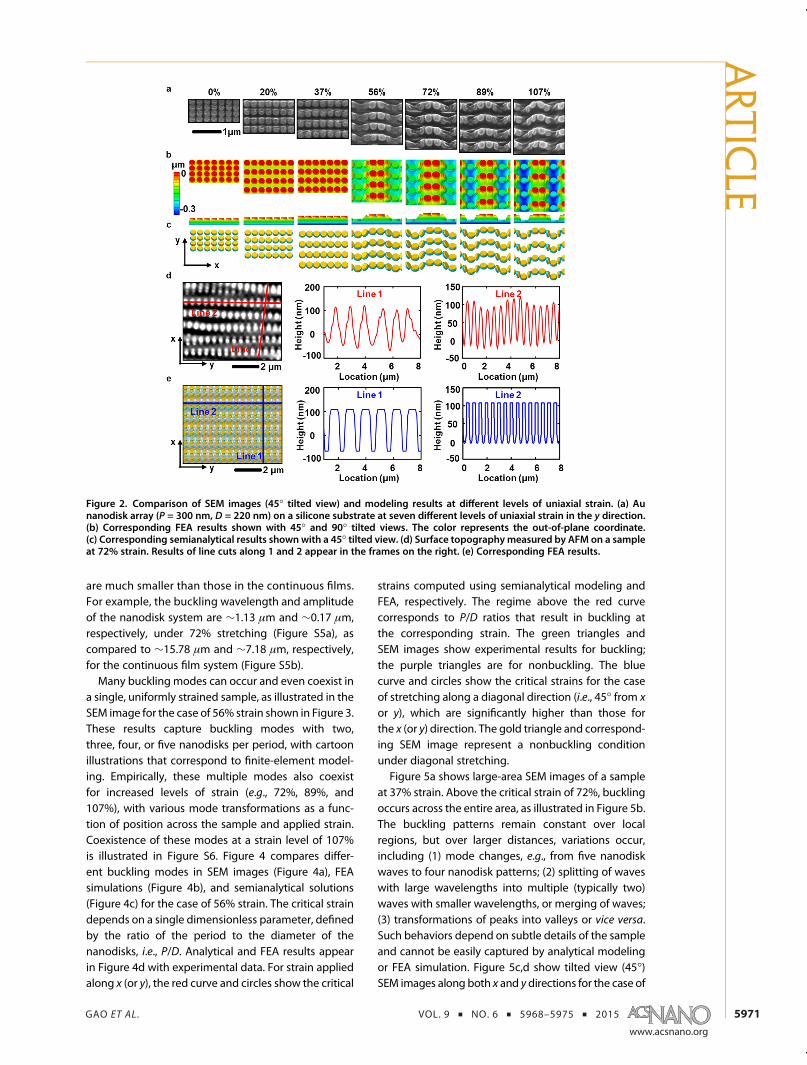
or y), which are significantly higher than those forthe x (or y) direction. The gold triangle and correspond-ing SEM image represent a nonbuckling conditionunder diagonal stretching.Figure 5a shows large-area SEM images of a sample
at 37% strain. Above the critical strain of 72%, bucklingoccurs across the entire area, as illustrated in Figure 5b.The buckling patterns remain constant over localregions, but over larger distances, variations occur,including (1) mode changes, e.g., from five nanodiskwaves to four nanodisk patterns; (2) splitting of waveswith large wavelengths into multiple (typically two)waves with smaller wavelengths, or merging of waves;(3) transformations of peaks into valleys or vice versa.Such behaviors depend on subtle details of the sampleand cannot be easily captured by analytical modelingor FEA simulation. Figure 5c,d show tilted view (45�)SEM images along both x and y directions for the case of
Figure 2. Comparison of SEM images (45� tilted view) and modeling results at different levels of uniaxial strain. (a) Aunanodisk array (P = 300 nm, D = 220 nm) on a silicone substrate at seven different levels of uniaxial strain in the y direction.(b) Corresponding FEA results shown with 45� and 90� tilted views. The color represents the out-of-plane coordinate.(c) Corresponding semianalytical results shown with a 45� tilted view. (d) Surface topographymeasured by AFM on a sampleat 72% strain. Results of line cuts along 1 and 2 appear in the frames on the right. (e) Corresponding FEA results.
ARTIC
LE

GAO ET AL . VOL. 9 ’ NO. 6 ’ 5968–5975 ’ 2015
www.acsnano.org
5972
107% strain, with examples of each of these three typesof variations. Complete sets of SEM images at differentstrains are in Figures S7 and S8. Figure S9 shows defect-free, large-area patterns (∼10000 μm2) at large strain.
DISCUSSION
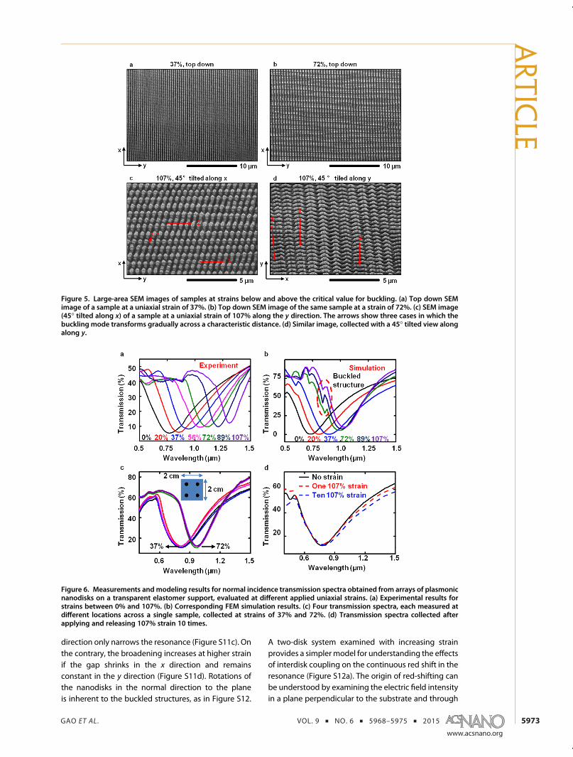
Figure 6a presents transmission spectra measuredfor a single sample at seven different strains, normal-ized to a bare silicone substrate. The light sourceis polarized in the x direction, perpendicular to thestretching direction. Transmission spectra measuredwith light polarized parallel to the stretching direction(Figure S10) show comparatively smaller tunabilitywith strain. The as-fabricated sample (nanodisks with aperiod of 300 nm and a diameter of 220 nm) has aresonance located at∼770 nm. Strain induces a red shift
in this resonance, ultimately to a center wavelength of1310 nm at 107%. The onset of buckling does not leadto a significant alteration in the nature of the straindependence of the resonance peak, although at largestrains, the depth and width of the resonance increaseand decrease, respectively. Optical simulations canprovide insights into the influence of various strain-induced motions of the nanodisks, which revealsthat the red shifts in resonance are caused by bothsheet deformation and buckling geometry. The effectsof changes in spacings along the x and y directionsappear in Figure S11. Increases in the spacing along they direction and decreases in the x direction yield auniform red shift in the resonance wavelength, similarto experiment (Figure S11b). Maintaining fixed spacingin the x direction and increasing the spacing in the y
Figure 3. SEM images (top down view) and corresponding modeling results that show different buckling modes across asingle sample at a strain of 56%. Bucklingmodes with two, three, four, and five nanodisks in a single period can be observed.The insets provide additional SEM images and corresponding cross sectional views of FEA results.
Figure 4. SEM images (top down view) and correspondingmechanicalmodeling results for different bucklingmodes. (a) SEMimages of five different buckling modes that coexist at 56% uniaxial strain (along the y direction). These modes have two,three, four, or five nanodisks in a single period. (b) Top down and side views of FEA results. The color represents the out-of-plane coordinate. (c) Top down view of semianalytical results. (d) Analytical (lines) and FEA (circles) predictions of criticalbuckling strains under horizontal (red) and diagonal (blue) stretching, along with experimental verification (triangles) fordifferent cases. The purple triangles and corresponding micrographs show nonbuckling conditions under horizontalstretching; green triangles and corresponding micrographs show buckling conditions under horizontal stretching; goldtriangle and corresponding micrograph show a nonbuckling condition under diagonal stretching.
ARTIC
LE
GAO ET AL . VOL. 9 ’ NO. 6 ’ 5968–5975 ’ 2015
www.acsnano.org
5973
direction only narrows the resonance (Figure S11c). Onthe contrary, the broadening increases at higher strainif the gap shrinks in the x direction and remainsconstant in the y direction (Figure S11d). Rotations ofthe nanodisks in the normal direction to the planeis inherent to the buckled structures, as in Figure S12.
A two-disk system examined with increasing strainprovides a simplermodel for understanding the effectsof interdisk coupling on the continuous red shift in theresonance (Figure S12a). The origin of red-shifting canbe understood by examining the electric field intensityin a plane perpendicular to the substrate and through
Figure 5. Large-area SEM images of samples at strains below and above the critical value for buckling. (a) Top down SEMimage of a sample at a uniaxial strain of 37%. (b) Top down SEM image of the same sample at a strain of 72%. (c) SEM image(45� tilted along x) of a sample at a uniaxial strain of 107% along the y direction. The arrows show three cases in which thebuckling mode transforms gradually across a characteristic distance. (d) Similar image, collected with a 45� tilted view alongalong y.
Figure 6. Measurements and modeling results for normal incidence transmission spectra obtained from arrays of plasmonicnanodisks on a transparent elastomer support, evaluated at different applied uniaxial strains. (a) Experimental results forstrains between 0% and 107%. (b) Corresponding FEM simulation results. (c) Four transmission spectra, each measured atdifferent locations across a single sample, collected at strains of 37% and 72%. (d) Transmission spectra collected afterapplying and releasing 107% strain 10 times.
ARTIC
LE

GAO ET AL . VOL. 9 ’ NO. 6 ’ 5968–5975 ’ 2015
www.acsnano.org
5974
the center of the disks, which is plotted in Figure S12b.Each profile is shown at the wavelength specified bythe minimum of the transmission dip for that strain. Inthe linear strain regime, as the disks approach eachother, the local field intensities increase due to en-hanced capacitive coupling between the disks. Physi-cally, the edges of each disk form a capacitor, and asthe gap between the disks shrinks, the capacitanceincreases. The result is an enhancement of local electricfield and lowering of the resonant frequency of thesystem (i.e., red-shifting). As the disks buckle and rotaterelative to each other, the intensity of the hot spotcontinues to increase, which is indicative of evengreater capacitive coupling and red shifting. The rota-tion of the disks yields two geometric effects thatenhance coupling. First, the physical distance betweenthe edges of the metal disks decreases, thereby in-creasing the capacitance. Second, as the metal diskstouch and then rotate as they buckle, the effectiveinteraction surface area between the disks increases,which also increases the capacitance. Additional stud-ies of the effect of rotation angles for the two-disk gapmode appear in Figure S13a. Figure S13b,c comparethe transmission spectra of two-disk and four-disk gapmodes.The mechanical calculations provide accurate struc-
tural information for optical simulations, by both nu-merical and analytical techniques. Simulation resultsbased on waves that consist of five nanodisks perperiod appear in Figure 6b, where the strain variesfrom 0 to 107%. The results indicate that increasinglevels of strain lead to systematic red shifts of theplasmon resonance peak, along with slight decreasesin its depth and width. A coupling-dipole approxima-tion method described in Figure S14 shows similarresults; that is, the resonance peak red shifts withincreasing strain. These overall trends are consistentwith experimental results. The quantitative differencesmay arise, at least in part, from the various buck-ling modes that occur across the probed area of thesample. Accordingly, the measured transmission spec-tra correspond to an averaged optical response overall possible bucklingmodes, each of which has different
resonance and diffraction peaks. Additional simula-tions of the four-disk buckling geometry (mode 3)reveal resonance and diffraction peaks at longerwavelengths, up to ∼1300 nm for the highest strainlevels (Figure S15). The simulations indicate that theline shapes of the transmission spectra depend on thebuckling geometry at large strains. We chose bucklingmode 5 for the simulations. We note the small dis-continuities in the simulation results (red dashed ovalin Figure 6b) arise from materials-independent diffrac-tion effects (Figure S16). Such features depend criticallyon the buckling geometry and therefore do not appearclearly in the experimental results due to the spatialheterogeneity of the buckling modes. In spite of thesespatial variations, the overall uniformity of the samplesis excellent, as illustrated throughmeasurement for thecases of 37% and 72% as shown in Figure 6c. Here, thetransmission spectra are collected with a probingspot with a diameter of 3 mm, at locations separatedby 1 cm across a sample with an area of 4 cm2. Asexpected, the strain-induced spectral changes arerecoverable, due to the purely elastic nature of thedeformations. Figure 6d compares the transmissionspectra before applying strain and after releasing astrain of 107%.
CONCLUSIONS
The unusual mechanical and optical properties oflarge-area, ultrastretchable, and tunable plasmonicstructures like those introduced here offer strongpotential in realizing different types of three-dimen-sional optical structures and epidermal photonic sen-sors with properties that can be reversibly adjustedthrough applied strain. With mechanical and opticalmodeling approaches illustrated here, complicatedphotonic components and structures can be designedto yield an otherwise impossible three-dimensionalstructures upon buckling, with uniaxial, biaxial, orradial strains. New plasmonic resonance features couldbemadepossible, with additional real-time, wide-bandtuning capabilities. Strain-induced color change andlow-cost wearable plasmonic sensors represent addi-tional opportunities.
METHODS
Fabrication of the Silicon Stamp. Soft nanoimprint lithographyand oxygen plasma dry etching (PlasmaTherm, chamber pres-sure = 15 mTorr, RIE power = 50 W, O2 flow rate = 10 sccm)formed a polymermask on a siliconwafer, following proceduresdescribed elsewhere. Etching with a Bosch process (STS Inc.,chamber pressure = 94 mTorr, etch/passivation cycle time =5 s/5 s, RIE power = 20 W/0 W, SF6/C4F8 flow rate = 35 sccm/110 sccm, ICP power = 600 W) formed cylindrical features ofrelief on the silicon surface with a depth of ∼300 nm. Anotheroxygen plasma dry etching process removed the polymermask.Exposure to C4F8 in an ICP-RIE system (STS Inc., chamberpressure = 94 mTorr, passivation time = 15 s, RIE power = 0 W,C4F8 flow rate = 110 sccm, ICP power = 600 W) formed an
ultrathin (∼10 nm), uniform coating of a cross-linked fluoropo-lymer to facilitate release in the transfer process by reducing thedegree of adhesion between the depositedmultilayer stacks andthe underlying silicon.
Deposition of Multilayer Material Stacks by Electron Beam Evaporation.The plasmonic metal films (Au, Ag, and Al), the titanium layer(adhesion promoter for the plasmonic metals), and the film ofSiO2 (top surface bonding layer to enable transfer printing)weredeposited using an AJA International 6-pocket electron beamevaporator. Typical chamber base pressures were 1.0 � 10�8
Torr, and deposition rates were 0.1�0.15 nm/s.Transfer Printing to Elastomeric Substrates. A low-modulus, tacky
form of PDMS, created by mixing in a 35:1 ratio by weighingbase and curing agent of a commercial material (Sylgard 184,
ARTIC
LE

GAO ET AL . VOL. 9 ’ NO. 6 ’ 5968–5975 ’ 2015
www.acsnano.org
5975
Dow Corning), served as the substrate. Exposing this material toozone created by deep ultraviolet light (BHK Inc., grid lamp,model 88-9102-02) for 3.5 min formed reactive�OH groups onits surface. Contact with the multilayer material stacks on theraised regions of the silicon stamp initiated condensationreactions between the hydroxyl groups on the PDMS and thoseon the top surface layer of SiO2. Mild heating at 110 �C for 25 sled to strong bonding, such that peeling the PDMS awaytransferred an array of circular disks, in their entirety, from thetop surface of the silicon stamp.
Optical Measurements. Transmission spectra were collectedusing a Varian Cary 5G UV�vis�NIR spectrophotometer, con-figured with a slit with a diameter of 3 mm and a polarizeroriented perpendicular to the stretching direction. Transmis-sion spectra were normalized using a bare PDMS substrate.
Conflict of Interest: The authors declare no competingfinancial interest.
Supporting Information Available: Supplementary Notes1�4 and Figures S1�S16 provide additional information forthe results described throughout the main text. The SupportingInformation is available free of charge on the ACS Publicationswebsite at DOI: 10.1021/acsnano.5b00716.
Acknowledgment. This work was supported by the Office ofNaval Research under Grant N00014-10-1-0989.
REFERENCES AND NOTES1. Khang, D. Y.; Jiang, H.; Huang, Y.; Rogers, J. A. A Stretchable
Form of Single-Crystal Silicon for High-Performance Elec-tronics on Rubber Substrates. Science 2006, 311, 208–212.
2. Sun, Y.; Choi, W. M.; Jiang, H.; Huang, Y. Y.; Rogers, J. A.Controlled Buckling of Semiconductor Nanoribbons forStretchable Electronics. Nat. Nanotechnol. 2006, 1, 201–207.
3. Sun, Y.; Kumar, V.; Adesida, I.; Rogers, J. A. Buckled andWavy Ribbons of GaAs for High-Performance Electronicson Elastomeric Substrates. Adv. Mater. 2006, 18, 2857–2862.
4. Jiang, H.; Khang, D.-Y.; Song, J.; Sun, Y.; Huang, Y.; Rogers,J. A. Finite Deformation Mechanics in Buckled Thin Filmson Compliant Supports. Proc. Natl. Acad. Sci. U.S.A. 2007,104, 15607–15612.
5. Choi, W. M.; Song, J.; Khang, D.-Y.; Jiang, H.; Huang, Y. Y.;Rogers, J. A. Biaxially Stretchable “Wavy” Silicon Nano-membranes. Nano Lett. 2007, 7, 1655–1663.
6. Sun, Y.; Rogers, J. A. Structural Forms of Single CrystalSemiconductor Nanoribbons for High-PerformanceStretchable Electronics. J. Mater. Chem. 2007, 17, 832–840.
7. Kim, D.-H.; Lu, N.; Ma, R.; Kim, Y.-S.; Kim, R.-H.; Wang, S.; Wu,J.; Won, S. M.; Tao, H.; Islam, A.; Yu, K. J.; et al. EpidermalElectronics. Science 2011, 333, 838–843.
8. Webb, R. C.; Bonifas, A. P.; Behnaz, A.; Zhang, Y.; Yu, K. J.;Cheng, H.; Shi, M.; Bian, Z.; Liu, Z.; Kim, Y. S.; et al. UltrathinConformal Devices for Precise and Continuous ThermalCharacterization of Human Skin. Nat. Mater. 2013, 12, 938.
9. Pryce, I. M.; Aydin, K.; Kelaita, Y. A.; Briggs, R. M.; Atwater,H. A. Highly Strained Compliant Optical Metamaterialswith Large Frequency Tunability. Nano Lett. 2010, 10,4222–4227.
10. Aksu, S.; Huang, M.; Artar, A.; Yanik, A. A.; Selvarasah, S.;Dokmeci, M. R.; Altug, H. Flexible Plasmonics on Uncon-ventional and Nonplanar Substrates. Adv. Mater. 2011, 23,4422–4430.
11. Lee, M. H.; Huntington, M. D.; Zhou, W.; Yang, J. C.; Odom,T. W. Programmable Soft Lithography: Solvent-AssistedNanoscale Embossing. Nano Lett. 2010, 11, 311–315.
12. Gao, L.; Shigeta, K.; Vazquez-Guardado, A.; Progler, C. J.;Bogart, G. R.; Rogers, J. A.; Chanda, D. NanoimprintingTechniques for Large-Area Three-Dimensional NegativeIndex Metamaterials with Operation in the Visible andTelecom Bands. ACS Nano 2014, 8, 5535–5542.
13. Gao, L.; Kim, Y.; Vazquez-Guardado, A.; Shigeta, K.; Hartanto,S.; Franklin, D.; Progler, C. J.; Bogart, G. R.; Rogers, J. A.;
Chanda, D. Materials Selections and Growth Conditionsfor Large-Area, Multilayered, Visible Negative Index Meta-materials FormedbyNanotransfer Printing.Adv. Opt.Mater.2014, 2, 256–261.
14. Chen, X.; Hutchinson, J. W. Herringbone Buckling Patternsof Compressed Thin Films on Compliant Substrates.J. Appl. Mech. 2004, 71, 597–603.
ARTIC
LE