Chapter4 Transmitters and Receivers Generalized Transmitters AM PM Generation
Upload
nguyentuyenCategory
view
215download
3
7 Optical Transmitters
Having completed our discussion of the optical receiver, we now turn to the trans- mitter. We start with a brief discussion of the transmitter specifications. Then, we focus on the devices used for the electrical-to-optical conversion, namely, the laser and the modulator. Their characteristics are important for the driver design as well as the transmission system design.
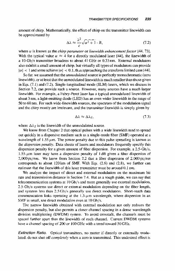
Types of Modulation. Figure 7.1 illustrates two alternative ways to generate a modulated optical signal. In Fig. 7.1 (a), the laser is turned on and off by modulating its current; this method is known as direct modulation. In Fig. 7.l(b), the laser is on at all times, a so-called continuous wave (CW) laser, and the light beam is modulated with a kind of optoelectronic shutter, a so-called modulator; this method is known as external modulation. Direct modulation has the advantages of simplicity, compactness, and cost effectiveness, whereas external modulation can produce higher-quality optical pulses, permitting extended reach and higher bit rates.
Direct as well as external modulation can be used to produce non-return-to-zero ( N U ) or return-to-zero (RZ) modulated optical signals. However, to produce very high-speed RZ-modulated signals, a cascade of two optical modulators, known as a tandem modulator, frequently is used. In this arrangement, the first optical modulator modulates the light from the CW laser with an NRZ signal and the second modulator, which is driven by a clock signal, coniverts the NRZ signal to an RZ signal in the optical domain.
233
Broadband Circuitsfor Optical Fiber Communication. Eduard SSLckinger Copyright 0 2005 by John Wiley & Sons, Inc.
ISBN: 0-47 1-7 1233-7

234 OPTICAL TRANSMITTERS
SLM Laser Chirped Swctrum
D” SLM Laser Modulator w
>B
Transform Limited Spectrum
= + ^ h . f 4+-
B
Fig. 7.1 Optical transmitters: (a) direct modulation vs. (b) external modulation.
7.1 TRANSMllTER SPECIFICATIONS
In the following, we look at two important specifications of the optical transmitter: (i) the spectral linewidth and (ii) the extinction ratio. The values that can be achieved for these parameters depends on whether direct or external modulation is used.
Spectral Linewidth. For a perfectly monochromatic light source followed by a per- fect intensity modulator, the optical spectrum of the modulated output signal looks like that of an amplitude-modulated (AM) transmitter: a carrier and two sidebands corresponding to the spectrum of the baseband signal. In the case of an NRZ modu- lation, the spectrum looks as shown in Fig. 7.l(b). The 3-dB bandwidth of one NRZ sideband is about half the bit rate, B / 2 , and thus the full bandwidth, which covers both sidebands, is about equal to the bit rate.’ If we convert this bandwidth or frequency linewidth to the commonly used wavelength linewidth, we get
where h is the wavelength and c is the speed of light in vacuum (c = 3 . lo8 m/s). For example, at 10 Gb/s, the frequency linewidth is about I0 GHz, corresponding to a wavelength linewidth of 0.08nm for A = 1.55 pm. In practice, it is difficult to build a transmitter with a linewidth as narrow as this; only some types of external modulators can come close to this ideal. Optical pulses that do have this narrow spectrum are known as transform limited pulses.
For most transmitters, the modulation process not only changes the light’s am- plitude but also its phase or frequency. This unwanted frequency modulation (FM) is called chirp and causes the spectral linewidth to broaden as shown in Fig. 7.l(a). The directly modulated laser is a good example for a transmitter with a significant
‘The full bandwidth measured null-to-null is 2B.
TRANSMITER SPECIFICATIONS 235
amount of chirp. Mathematically, the effect of chirp on the transmitter linewidth can be approximated by
h.2 Ah x -d-' ( Y ~ + 1 . B ,
17 (7.2)
where (Y is known as the chirp parameter or linewidth enhancement factor [44, 731. With the typical value (Y x 4 for a directly modulated laser [a], the linewidth of a 10-Gb/s transmitter broadens to about 41 GHz or 0.33 nm. External modulators also exhibit a small amount of chirp, but virtually all types of modulators can provide la I i 1 and some achieve la! I < 0.1, thus approaching the transform limited case [a].
So far, we assumed that the unmodulated source is perfectly monochromatic (zero linewidth), or at least that the unmodulated linewidth is much smaller than those given in Eqs. (7.1) and (7.2). Single-longitudinal mode (SLM) lasers, which we discuss in Section 7.2, can provide such a source. However, many sources have a much larger linewidth. For example, a Fabry-Perol: laser has a typical unmodulated linewidth of about 3 nm, a light-emitting diode (LED) has an even wider linewidth in the range of 50 to 60 nm. For such wide-linewidth >iowces, the spectrum of the modulation signal and the chirp mostly are irrelevant, and the transmitter linewidth is simply given by
Ah Ahs, (7.3)
where Ahs is the linewidth of the unmodulated source. We know from Chapter 2 that optical pulses with a wide linewidth tend to spread
out quickly in a dispersive medium such as a single-mode fiber (SMF) operated at a wavelength of 1.55 pm. The power penalty due to this pulse spreading is known as the dispersion penalty. Data sheets of lasers and modulators frequently specify this dispersion penalty for a given amount of fiber dispersion. For example, a 2.5-Gb/s, 1.55-pm laser may have a dispersion penalty of 1 dB given a fiber dispersion of 2,00Ops/nm. We know from Section 2.2 that a fiber dispersion of 2,00Ops/nm corresponds to about 120km of SMF. With Eqs. (2.6) and (2.8), we further can estimate that the linewidth of this laser transmitter must be around 0.1 nm.
We analyze the impact of direct and external modulation on the maximum bit rate and transmission distance in Section 7.4. But as a rough guide, we can say that telecommunication systems at 10 Gb/s and more generally use external modulation, 2.5-Gb/s systems use direct or externla1 modulation depending on the fiber length, and systems less than 2.5 Gb/s generally use direct modulation. Short-reach data communication links operating at the 1.3-pm wavelength, where dispersion in an SMF is small, use direct modulation even at 10Gb/s.
The narrow linewidth obtained with external modulation not only reduces the dispersion penalty, but also permits a closer channel spacing in a dense wavelength division multiplexing (DWDM) system. To avoid crosstalk, the channels must be spaced further apart than the linewidth of each channel. Current DWDM systems have a channel spacing of 200 or 100 GHz with a trend toward 50 GHz.
Extinction Ratio. Optical transmitters, no matter if directly or externally modu- lated. do not shut off completely when a zero is transmitted. This undesired effect is
236 OPTICAL TRANSMI7TERS
quantified by the extinction ratio (ER), which is defined as follows2:
p1 ER=--, PO
(7.4)
where PO is the optical power emitted for a zero and P1 the power for a one. Thus, an ideal transmitter would have an infinite ER. The ER usually is expressed in dBs using the conversion rule 10 log ER. Typically, ERs for directly modulated lasers range from 9 to 14 dB, whereas ERs for externally modulated lasers can exceed 15 dB [29]. SONETKDH transmitters typically are required to have an ER in the range of 8.2 to 10 dB, depending on the application.
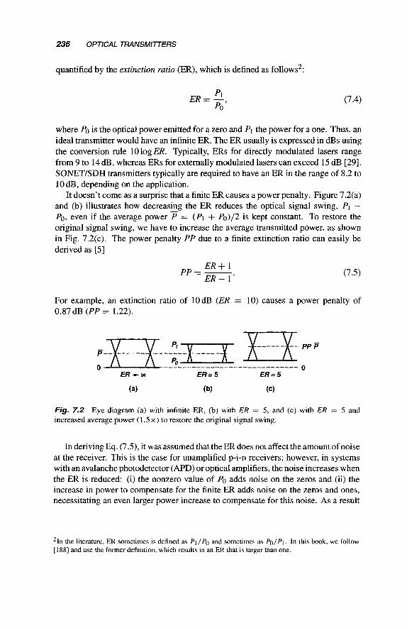
It doesn't come as a surprise that a finite ER causes a power penalty. Figure 7.2(a) and (b) illustrates how decreasing the ER reduces the optical signal swing, P1 - PO, even if the average power = ( P I + P0)/2 is kept constant. To restore the original signal swing, we have to increase the average transmitted power, as shown in Fig. 7.2(c). The power penalty PP due to a finite derived as [5]
ER+ 1 PP= -
ER- 1 '
extinction ratio can easily be
(7.5)
For example, an extinction ratio of l O d B (ER = 10) causes a power penalty of 0.87dB (PP = 1.22).
Fjg, 7.2 Eye diagram (a) with infinite ER, (b) with ER = 5, and (c) with ER = 5 and increased average power (1.5 x ) to restore the original signal swing.
In deriving Eq. (7.5), it was assumed that the ER does not affect the amount of noise at the receiver. This is the case for unamplified p-i-n receivers; however, in systems with an avalanche photodetector (APD) or optical amplifiers, the noise increases when the ER is reduced: (i) the nonzero value of PO adds noise on the zeros and (ii) the increase in power to compensate for the finite ER adds noise on the zeros and ones, necessitating an even larger power increase to compensate for this noise. As a result
*In the literature, ER sometimes is defined as PI /Po and sometimes a.. P ( ) / P l . in this book, we follow [ 1881 and use the former definition, which results in an ER that is larger than one.

LASERS 237
of these two mechanisms, the power penalty becomes larger than given in Eq. (7.5). If we take the extreme case where the: receiver noise is dominated by the detector (or optical amplifier) noise such that the electrical noise power is proportional to the received signal current, we find [29] that
a R i - 1 ERi -1 .- PP = f i R - 1 ER-1’
(7.6)
For example, an extinction ratio of 10 clB (ER = 10) causes a power penalty of up to 3.72dB (PP = 2.35) in an amplified lightwave systems. [+ Problem 7.11
In regulatory standards, the receiver sensitivity usually is specified for the worst- case extinction ratio. Therefore, the corresponding power penalty must be deducted from the sensitivity based on ER + 00, as given for example by Eq. (4.21). Typically, 2.2 dB (for ER = 6 dB) must be deducted in short-haul applications, and 0.87 dB (for ER = IOdB) must be deducted in long-haul applications [37].
Instead of specifying the average transmitter power, the optical modulation am- plitude (OMA), which is defined as PJ - PO and measured in dBm, can be used to measure the transmitter power. The OMA measure is used, for example, in 10-GbE systems. If the transmitter power and the receiver sensitivity are specified in terms of OMA rather than average power, a finite extinction ratio causes much less of a power penalty (no power penalty in the case of constant noise).
7.2 LASERS
In telecommunication systems, the Fabry-Peror (FP) laser and the distributed- feedback (DFB) laser are the most commonly used lasers. In data communication systems, such as Gigabit Ethernet, the FP laser and the vertical-cavity suqace-emitting laser (VCSEL) are preferred because of their lower cost. In low-speed data communi- cation (up to about 200 Mb/s) and consumer electronics, light-emitting diodes (LEDs) also find application as an optical source. The FP laser, DFB laser, and VCSEL are so-called semiconductor lasers or laseiv diodes, whereas the LED is not a laser. Fig- ures 7.3 and 7.4 show photos of a cooled and uncooled DFB laser, respectively.
In the following, we give a brief description of the FP laser, DFB laser, VCSEL, and LED. Then, we summarize the main characteristics of these light sources. More information on lasers and their properties can be found in [ S , 73, 183, 1841.
fabry-Perot Laser. The FP laser consists of an optical gain medium located in a cavity formed by two reflecting facets, as shown in Fig. 7.5(a). In a semiconductor laser, the gain medium is formed by i3 forward biased p-n junction, which injects carriers (electrons and holes) into a thin active region. These carriers “pump” the active region such that an incoming photon can stimulate the recombination of an electron-hole pair to produce a second identical photon. Thus, stimulated emission provides optical gain if the bandgap energy, that is, the energy released by the electron-

238 OPTICAL TRANSMITTERS
Fig. 7.3 Cooled 2.S-Gb/s DFB laser in a 14-pin butterfly package with single-mode fiber pigtail (2.1 cm x 1.3 cm x 0.9 cm). The pins provide access to the laser diode, monitor pho- todiode, thermoelectric cooler, and temperature sensor. Reprinted by permission from Agere Systems, Inc.
Fig. 7.4 (1.3 cm x 0.7 cm x 0.5 cm). Reprinted by permission from Agere Systems, Inc.
Uncooled 2.S-Gb/s DFB laser in an 8-pin package with single-mode fiber pigtail

LASERS 239
n-lnP
’ Facet
Grating - Fig. 7.5 Edge-emitting lasers (schematically): (a) Fabry-Perot laser vs. (b) distributed- feedback laser. The light propagates in the direction of the arrow.
hole pairs, matches the energy of the photons to be amplified.3 In Fig. 7.5, the active region is a layer of InGaAsP, which can be lattice matched to the surrounding InP layers and the substrate. Interestingly, the bandgap of the InxGa~-,As,,P~ -,, compound can be controlled by the mixing ratios x and y to provide optical gain anywhere in the 1.0- to 1.6-pm range. Thus, 1.3-pm as well as 1.5-pm lasers can be based on an InGaAsP active layer. ‘The surrounding p- and n-doped regions are made from InP, which has a wider bandgap than the active InGaAsP material, helping to confine the carriers to the active region. Short-wavelength lasers, operating at the 0.85-pm wavelength, typically use GaAs for the active layer and the wider bandgap AlGaAs material for the p- and n-doped regions (AlGaAs is lattice matched to the GaAs layer and substrate). In practical lasers, the active region usually is structured as a multiple quantum well (MQW), resulting in better performance than the simple structure shown in Fig. 7.5. [-+ Probleim 7.21
The separation of the two facets, the cavity length, determines the wavelengths at which the laser can operate. If the cavity contains a whole number of wavelengths and the net optical gain is larger than one, lasing occurs. Because the facets in an FP laser are many wavelengths apart (about 300 pm), there are multiple modes satisfying these conditions. FP lasers therefore belong to the class of multiple-longitudinal mode (MLM) lasers. As a result, the spectrum of the emitted laser light has multiple peaks, as shown on the right-hand side of Fig. 7.S(a). The corresponding spectral linewidth is quite large, typically around Ahs = 3 nm. FP lasers therefore are used primarily at the 1.3-pm wavelength where dispersion in an SMF is low.
Most FP lasers are operated as uncooled lasers, which means that their temperature is not controlled and can go up to around 85°C. This mode of operation simplifies the transmitter design and keeps its cost low, but has the drawbacks of varying laser characteristics and reduced laser reliability.
”Laser is an acronym for “Light Amplification b y Stimulated Emission of Radiation.” The gain medium also can be used without the facets and then is known as a semiconductor opricul amplifier (SOA), rather than a laser.

240 OPTICAL TRANSMITTERS
Distributed-Feedback Laser. The DFB laser consists of a gain medium, similar to that in an FP laser, with a built-in grating, which acts as a reflector, as shown in Fig. 7.5(b). The grating can, for example, be implemented by etching a corrugation near the active layer. In contrast to the facets of the FP laser, the grating provides distributed feedback and selects only one wavelength for amplification as shown on the right-hand side of Fig. 7.5(b). For this reason, DFB lasers belong to the class of single-longitudinal mode (SLM) lasers. The emitted spectrum of an unmodulated DFB laser has a very narrow linewidth, typically Ahs < 0.001nm (<100MHz). When the laser is directly modulated, the linewidth broadens because of the AM sidebands and chirp, as discussed in Section 7.1.
The distributed Bragg reflector (DBR) laser is similar to the DFB laser in the sense that it also operates in a single longitudinal mode, producing a narrow linewidth. In terms of structure, it looks more like an FP laser, however, with the facets replaced by wavelength-selective Bragg mirrors (gratings).
DFBDBR lasers are suitable for direct modulation as well as for CW sources fol- lowed by an external modulator. Because of their narrow linewidth, they are ideal for WDM and DWDM systems. Unfortunately, the wavelength emitted by a semicon- ductor laser is slightly temperature dependent, for example, a variation of 0.1 nm/"C is typical for a DFB laser. Given a DWDM system with a 0.8-nm wavelength spacing ( 1 00-GHz grid), the laser temperature must be controlled precisely. Therefore, many DFBDBR lasers are operated as cooled lasers. Such lasers are mounted on top of a thermoelectric cooZer (TEC), which is controlled by a feedback loop and a thermistor to stabilize the temperature.
Vertical-Cavity Surface-Emitting Laser. The VCSEL emits the light perpendic- ular to the wafer surface rather than at the edges of the chip (parallel to the wafer surface), as the FP or DFBDBR lasers do. The VCSEL consists of a gain medium located in a very short vertical cavity (about 1 pm) with Bragg mirrors at the bottom and the top as shown in Fig. 7.6(a). The Bragg mirrors are formed by many layers of alternating high and low refractive-index material. Because of the short cavity length, the longitudinal modes are spaced far apart and just one of them has a net optical gain larger than one, thus the VCSEL also belongs to the class of SLM laser. However, depending on the horizontal size, VCSELs have multiple transverse modes, causing a wider spectral linewidth than the DFBDBR lasers, typically Ahs x 1 nm. Also, VCSELs typically are less powerful than DFBDBR lasers.
The advantage of VCSELs over edge-emitting lasers is that they can be fabricated, tested, and packaged more easily and at a lower cost. However, the very short length of the gain medium requires mirrors with a very high reflectivity to make the net gain larger than one. Currently, VCSELs are commercially available at short wavelengths (0.85-j~m band) where fiber loss is appreciably high. Long-wavelength VCSELs are under development. The application of short-wavelength VCSELs mostly is in data communication systems using multimode fiber (MMF).
Light-Emitting Diode. The LED operates on the principle of spontaneous emission rather than stimulated emission. and therefore is not a laser. The LED consists of a

LASERS 241
t ztr pAlGaAs
n-AIGa As
Fig. 7.6 vs. (b) light-emitting diode. The light propagates in the direction of the arrow(s).
Surface-emitting sources (schematically): (a) vertical-cavity surface-emitting laser
forward biased p-n junction without any mirrors or gratings, as shown in Fig. 7.6(b). The electron-hole pairs injected into the active region recombine spontaneously, emit- ting photons with an energy that corresponds to the bandgap energy. As a result, the light is emitted in all directions and it is difficult to couple much of it into a fiber. For example, an LED may couple 10 /IW optical power into a fiber, whereas a laser easily can produce 1 mW. Furthermore, because there is no mechanism to select a single wavelength, the spectral linewidth is very wide, typically Aks = SO to 60 nm. The modulation speed of an LED is limited by the carrier lifetime to a few hundred Mb/s, whereas a fast laser can be modulated in excess of 10 Gb/s.
On the plus side, LEDs are very low in cost, they are more reliable than lasers, and they are easier to drive because they lack the temperature-dependent threshold current typical for lasers. Their application mostly is in short-reach data communication systems using MMF.
I N Characteristics. From an electrical point of view, the semiconductor laser is just a forward-biased diode. The relationship between the laser current, ZL, and the forward-voltage drop, VL, is described by the so-called IN curve. Figure 7.7(a) shows an I/V curve that is typical for an edge-emitting InGaAsP laser. For such a laser, the small-signal resistance is normally in the range of 3 to 8 S2, whereas the forward-voltage drop varies from 0.7 to 2.2 V, depending on the current, temperature, age, and bandgap of the semiconductor materials used. The IN curve of a VCSEL exhibits a larger small-signal resistance, often in the neighborhood of SO S2.
Fig. 7.7 (a) Typical I/V curve of an edge-emitting InGaAsP laser and (b) the corresponding large-signal AC model for a lO-Gb/s part.
242 OPTICAL TRANSMITTERS
A simple large-signal AC model for the semiconductor laser is shown in Fig. 7.7(b); the values shown are typical for a 10-Gb/s, edge-emitting InGaAsP laser. At low cur- rents, the diode determines the forward-voltage drop and the small-signal resistance ( V T / I L ) . At high currents, the contact resistance (6 !2 in Fig. 7.7(b)) adds a significant amount of voltage drop and dominates the overall small-signal resistance. It thus is the contact resistance that determines the slope of the W curve at normal operating currents. The capacitor (2pF in Fig. 7.7(b)) models the junction and diffusion capac- itance of the forward-biased p-n junction and typically is fairly large, especially when compared with the capacitance of a corresponding photodiode. Compared with edge- emitting lasers, the much smaller VCSELs tend to have a larger contact resistance and a smaller junction capacitance. To model a packaged laser, additional elements, such as the bond-wire inductance, must be added to the equivalent circuit in Fig. 7.7(b).
Some packaged lasers contain a series resistor (e.g., 19 Q or 44 Q) to match the 6-Q laser resistance to that of the transmission line (e.g., 25 Q or SO Q) that connects the laser to its driver. If such a series resistor is used, an RF choke (RFC) usually is included as well to bypass the matching resistor, that is, to apply the bias current directly to the laser. Packaged lasers usually designate one electrode as ground and the other one as RF input. Typically, edge-emitting lasers designate the anode as ground, whereas VCSELs designate the cathode as ground.
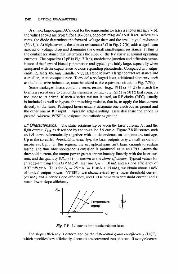
UI Characteristics. The static relationship between the laser current, I L , and the light output, Pout, is described by the so-called UI curve. Figure 7.8 illustrates such an L/I curve schematically together with its dependence on temperature and age. Up to the so-called threshold current, I T H , the laser outputs only a small amount of incoherent light. In this regime, the net optical gain isn't large enough to sustain lasing, and thus only spontaneous emission is produced, as in an LED. Above the threshold current, the output power grows approximately linearly with the laser cur- rent, and the quantity a P0,,/alL is known as the slope eficiency. Typical values for an edge-emitting InGaAsP MQW laser are ITH = 10 mA and a slope efficiency of 0.07 mW/mA. Thus for I L = 25 mA (= lOmA + 15 mA), we obtain about 1 mW of optical output power. VCSELs are characterized by a lower threshold current (4 mA) and a better slope efficiency, and LEDs have zero threshold current and a much lower slope efficiency.
Fig. 7.8 LII curves for a semiconductor laser.
The slope efficiency is determined by the dzyerential quantum eficienq (DQE), which specifies how efficiently electrons are converted into photons. If every electron

LASERS 243
produces a photon and they all are coupled into the fiber, the slope efficiency is hclhq, in analogy to the responsivity of a phlotodetector with 100% quantum efficiency (cf. Eq. (3.2)). At the wavelength h = 1.55 pm, this ideal slope efficiency is about 0.8 mW/mA. In practice, however, not all electrons produce photons, some photons are radiated out of the back facet, and not all photons from the front facet couple into the fiber, resulting in an about ten-fold lower slope efficiency. Note that as in the case of the photodetector, the optical power is linearly related to the electrical current through the device, which means that we carefully have to distinguish between optical and electrical dBs.
As indicated in Fig. 7.8, the laser characteristics, in particular ITH, are strongly temperature and age dependent. For example, a laser that nominally requires 25 mA to output 1 mW of optical power may require in excess of 50 mA at 85°C and near the end of life to output the same power. The temperature dependence of the threshold current is exponential and can be described by [S]
where ZTHO is the (extrapolated) threshold current at 0 K and TO is a constant in the range of 50 to 70 K for InGaAsP lasers. The temperature dependence of the laser’s slope efficiency is less dramatic, a 30% 10 40% reduction when heating the laser from 25°C to 85°C is typical.
Because of the strong temperature and age dependence of the laser’s L/I curve, communication lasers usually have a built-in monitor photodiode to measure the optical output power at the back facet of the laser. The current from this photodiode closely tracks the optical power coupled into the fiber with little dependence on temperature and age; a tracking error of f10% is typical. A feedback mechanism that compares the current from the monitor photodiode with a reference current and controls the laser current accordingly can be used to implement a so-called automatic power control (AFT). More on this subject in Section 8.2.6.
For analog applications, such as CATVMFC systems, the linearity of the L/I curve is another important laser parameter, besides the slope efficiency and the threshold current. A deviation from the linear characteristics causes harmonic and intermod- ulation distortions in the analog signal. In the case of a TV signal, these distortions degrade the picture quality. Typically, the laser linearity is specified by the com- posite second order (CSO) and composite triple beat (CTB) distortion parameters (cf. Section 4.8) measured at a certain laser current and modulation index.
Dynamic Behavior. The dynamic relationship between the laser current and the light output is quitecomplex. It is fully described by the so-called laser rate equations, two coupled, nonlinear, differential equations relating the carrier density and photon density in the laser cavity [5, 831. It IS beyond the scope of this book to discuss these equations. Instead, we just want LO give a verbal description of what happens in response to a laser-current pulse ramping up from zero and, after one or more bit periods, returning back to zero, as shown in Fig. 7.9(a).
244 OPTICAL TRANSMITERS
I Turn-On Delay & Jitter
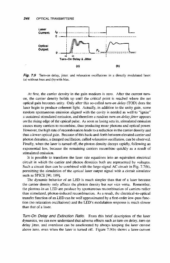
Fig. 7.9 Turn-on delay, jitter, and relaxation oscillations in a directly modulated laser: (a) without bias and (b) with bias.
At first, the carrier density in the gain medium is zero. After the current turn- on, the carrier density builds up until the critical point is reached where the net optical gain becomes unity. Only after this so-called turn-on delay (TOD) does the laser begin to produce coherent light. Actually, in addition to the unity gain, some random spontaneous emission aligned with the cavity is needed as well to “ignite” a sustained stimulated emission, and therefore a random turn-on delay jitter appears on the rising edge of the optical pulse. As soon as lasing sets in, stimulated emission causes many camers to recombine, thus producing more photons and optical power. However, the high rate of recombination leads to a reduction in the camer density and thus a lower optical gain. Because of this back-and-forth between elevated carrier and photon densities, a damped oscillation, called relaxation oscillation, can be observed. Finally, when the laser is turned off, the photon density decays rapidly, following an exponential law, because the remaining carriers recombine quickly as a result of stimulated emission.
It is possible to transform the laser rate equations into an equivalent electrical circuit in which the carrier and photon densities both are represented by voltages. Such a circuit then can be combined with the large-signal AC circuit in Fig. 7.7(b), permitting the simulation of the optical laser output signal with a circuit simulator such as SPICE [90, 1891.
The dynamic behavior of an LED is much simpler than that of a laser because the carrier density only affects the photon density but not vice versa. Remember, the photons in an LED are produce by spontaneous recombination of carriers rather than stimulated, photon-induced recombination. As a result, the electrical-to-optical transfer function of an LED can be well approximated by a first-order low-pass func- tion (no relaxation oscillations) and the LED’S modulation response is much slower than that of a laser.
Turn-On Delay and Extinction Ratio. From this brief description of the laser dynamics, we can now understand that adverse effects such as turn-on delay, turn-on delay jitter, and overshoot can be ameliorated by always keeping the laser current above zero, even when the laser is turned off. Figure 7.9(b) shows a laser-current

LASERS 245
pulse where this minimum current, known as bias current, is set to IB. If we bias the laser close to the threshold current, the carrier density is already built up and the net optical gain is close to unity, yet the photon density is still low. With just a little bit more current, the laser turns on quickly. A simple equation describes the TOD as follows [183]:
where tc is the carrier lifetime, which typically is around 3 ns, I B is the off-current or bias current, and I L . ~ ~ is the on-current. For a zero bias current, IB = 0, and the typical numbers I L . ~ ~ = 25 mA and ITH = 10 mA, we obtain a TOD of about 1.5 ns. However, if the laser is biased at I B = ITH = 10 mA, the TOD goes to zero. Note that lasers with a low threshold current have a small turn-on delay, even if they are operated without bias current. In practical transmitters, the laser is almost always biased near I T H , except in some low-speed applications (155 Mb/s and below) where it is possible to predistort the electrical signal to compensate for the TOD (cf. Section 8.3.3).
Biasing not only helps to improve the TOD but also reduces the turn-on delay jitter, the amplitude of the relaxation oscillations, and the optical chirp. However, there also is an important downside to biasing the laser near the threshold current: it lowers the extinction ratio. Even if the laser is not lasing at I B < ITH, it still produces a small amount of incoherent light, PO, as indicated in Fig. 7.9(b). In high-speed transmitters, the laser often is biased a little bit above ITH to improve its speed, however, at the expense of the ER. Typical ER values for high-speed semiconductor lasers are in the range of 9 to 14dB [29].
Modulation Bandwidth. The laser's modulation bandwidth determines the maxi- mum bit rate for which the laser can be used. This bandwidth is closely related to the frequency of the relaxation oscillations and thus depends on the interplay between the camer and photon densities as described by the rate equations. The small-signal modulation bandwidth for IB > ITH can be derived from the rate equations and is proportional to [5]
BW- ,/-. (7.9)
Thus, the more the laser is biased above the threshold current, the faster it becomes. For this reason, the laser in high-speed transmitters is biased as much above the threshold current as possible while still meeting the ER specification.
In contrast, the LED's modulation bandwidth mostly is determined by the camer lifetime, r,, and can be expressed as BW = f i / ( 2 n s c ) [5]. Thus, the LED's speed does not depend strongly on the bias current.
Chirp. In Section 7.1, we introduced the chirp parameter a , which describes the transmitter's spurious frequency moduiation (FM). More precisely, the a parameter relates the optical frequency excursion, A f , to the change in optical output power, Pout, as follows [73]:
(7.10)

246 OPTICAL TRANSMITTERS
This relationship holds for direct as well as external modulation. With a positive value for a, as is the case for directly modulated lasers, the frequency shifts slightly toward the blue when the output power is rising (leading edge) and toward the red when the power is falling (trailing edge). Directly modulated lasers produce chirp (a # 0) because the injected current not only modulates the optical gain and thus the output power, but also the refractive index of the gain medium and thus the optical frequency. [-+ Problem 7.31
From Eq. (7.10) we can see that slowing the rise and fall times of the laser-current pulses, and thus lowering the rate of change of Pout, helps to reduce the amount of chirp [ 1691. We further can conclude that large relaxation oscillations, causing a large rate of change of Pout, exacerbate the chirping problem.
Noise. The stimulated emission of photons in the laser produces a coherent elec- tromagnetic field. However, occasional spontaneous emissions add amplitude and phase noise to this coherent field. The results are a broadening of the (unmodulated) spectral linewidth and fluctuations in the intensity. The latter effect is known as rel- ative intensity noise (RIN). A p-i-n photodetector receiving laser light that contains intensity noise produces a corresponding electrical RIN noise, in,RIN, in addition to the fundamental (quantum) shot noise? For a given laser, the electrical FUN-noise power, i:,RIN, is approximately proportional to the received signal power, I j I N , [83]:
-
- i:%RIN = RIN . 1jN . BW,, (7.11)
where RIN is a parameter characterizing the laser RIN noise measured in dB/Hz. This means that the CW signal-to-noise ratio (SNR) at the receiver due to RIN noise is fixed at I&,,/i:,RIN = l/(RIN. BW,) and cannot be improved by increasing the laser
power. Note that this situation is very different from that of the detector noise, i:.pD, which was proportional to I ~ D as opposed to I;D. For example, given a laser with RIN = - 135 dB/Hz, the SNR due to RIN noise is 35 dB in a 10-GHz bandwidth, regardless of power. For the reception of a digital NRZ signal, this is more than enough and RIN noise often can be neglected in the analysis of digital transmission systems. However, in analog transmission systems, RIN noise is critical. For example, a CATVRIFC system using AM-VSB modulation typically is limited by RIN noise (cf. Section 5.2.12).
The effect of FUN noise on a digital transmission system can be quantified, as usual, with a power penalty. The RIN noise adds to the noise at the receiver, which means that we need to transmit more power to achieve the same bit-error rate (BER) as without RIN noise. The power penalty due to FUN noise is [5]
- -
1 PP =
I - Q . RIN . BW,; (7.12)
4Sorne authors include the shot noise as part of the RIN noise (e.g. [6]). but here we keep them separate.

MODULATORS 247
With the example values l/(RIN. BW,) = 35dB and BER = (Q = 7.035), the power penalty is only 0.068 dB (PP = 1.016). However, if the SNR due to RIN noise approaches Q2 = 49.5 (16.9dE), the power penalty becomes infinite. This can be explained as follows: we know from Eq. (4.13) that to receive an NRZ signal with much more noise on the ones than the zeros (as is the case for RIN noise), we need an SNR of at least 112 ‘ Q2. The SNR due to RIN noise of the unmodulated (CW) optical signal is l/(RZN . BW,)i, as given by Eq. (7.11). NRZ modulation reduces the signal power by a factor four and the noise power by a factor two, so the SNR due to RIN noise of the modulated signal becomes 1/(2 . RIN . BW,). Because the transmitted SNR must be higher than the required SNR at the receiver, we need l/(RIN. BW,) > Q2, in accordance with Eq. (7.12). [-+ Problem 7.41
In MLM lasers, such as FP lasers, as well as SLM lasers with an insufficient mode-suppression ratio (<20 dB), another type of noise called mode-partition noise (MPN) also is of concern. This noise is caused by power fluctuations among the various modes (mode competition) and is harmless by itself because the total intensity remains constant. However, chromatic dispersion in the fiber can desynchronize the mode fluctuations and turn them into additional RIN noise. Furthermore, a weak optical reflection of the emitted light back into the laser can create additional modes, further enhancing the RIN noise. These RIN-noise enhancing effects may be strong enough to reduce the received SNR below the critical value of 112. Q2. This situation manifests itself in a bit-error rate floor, that is, a minimum BER that cannot be reduced, regardless of the transmitted power [5].
Reliability The mean-time to failure (MTTF) of a typical semiconductor laser is between 1 and 10 years, if continuously operated at 70°C. When cooled down to room temperature, its lifetime extends by about a factor 1 Ox, to between 10 and 100 years [ 1741. In comparison, LEDs are rnuch more reliable and have an MTTF of 100 to 1,000 years when operated at 70°C.
These laserreliability numbers may not look so great, but they are much better than those of the early lasers. The first “continuous-wave’’ semiconductor laser that could operate at room temperature was demonstrated by researchers at the Zoffe Physical Institute in Leningrad in 1970. However, the lifetime of these GaAs lasers was measured in seconds; not very much of a continuous wave indeed! It took about seven years of tedious work until AT&TBell Laboratories could announce a semiconductor laser with a 100-year (million hour) lifetime [43].
7.3 MODULATORS
Two types of optical modulators commlonly are used in communication systems: the electroabsorption modulator (EAM) and the Mach-Zehnder modulator (MZM). The EAM is small and can be integrated with the laser on the same substrate, whereas the MZM is much larger but features superior chirp and ER characteristics. An EAM combined with a CW laser source is known as an electroabsorption modulated laser

248 OPTICAL TRANSMI77ERS
(EML). See Figs. 7.10 and 7.1 1 for photos of a packaged EML module and an MZ modulator, respectively.
In the following, we give a brief description of the two modulators and summarize their main characteristics. More information on modulators and their properties can be found in [ 1 , 3,4,44,73].
Electroabsorption Modulator. An EML consist of a CW DFB laser followed by an EAM, as shown in Fig. 7.12. Both devices can be integrated monolithically on the same InP substrate, leading to a compact design and low coupling losses between the two devices. The EAM consists of an active semiconductor region sandwiched in between a p- and n-doped layer, forming a p-n junction. The EAM works on the principle known as Franz-Keldysh effect, according to which the effective bandgap of a semiconductor decreases with increasing electric field. Without bias voltage across the p-n junction, the bandgap of the active region is just wide enough to be transparent at the wavelength of the laser light. However, when a sufficiently large reverse bias is applied across the p-n junction, the effective bandgap is reduced to the point where the active region begins to absorb the laser light and thus becomes opaque. In practical EAMs, the active region usually is structured as an MQW, providing a stronger field- dependent absorption effect (known as the quantum-conJined Stark effect) than the simple structure shown in Fig. 7.12.
The relationship between the optical output power, Pout, and the applied reverse voltage, V M , of an EAM is described by the so-called switching curve. Figure 7.13(a) illustrates such a curve together with the achievable ER for a given switching voltage, VSW. The voltage for switching the modulator from the on state to the off state, the switching voltage Vsw, typically is in the range of 1.5 to 4 V, and the dynamic ER usually is in the range of 11 to 13 dB [29,73]. Because the electric field in the active region not only modulates the absorption characteristics, but also the refractive index, the EAM produces some chirp. However, this chirp usually is much less than that of a directly modulated laser with the chirp parameter, (a/, typically being smaller than one. A small on-state (bias) voltage around 0 to 1 V often is applied to minimize the modulator chirp [3, 731.
From an electrical point of view, the EAM is just a reverse-biased diode. Thus, when the CW laser is off, the EAM impedance mostly is capacitive. For a 10-Gb/s modulator, the equivalent capacitor is about 0.1 to 0.15 pF, as shown in Fig. 7.13(b). When the CW laser is on, however, the photons absorbed in the EAM generate a photocurrent, pretty much like in a p-i-n photodetector. This current is a function of how much light is absorbed in the EAM, which in turn is a function of the modulation voltage, V M . Thus, the photocurrent can be described by an equivalent voltage- controlled current source, I ( V M ) , as shown in Fig. 7.1 3@). As a result of this current source, the capacitive load appears shunted by a nonlinear resistance, which has a high value when the EAM is completely turned on or off, but assumes a low value during the transition 176, 1371.
Packaged EAMs often contain a 5042 parallel resistor to match the modulator impedance to that of the transmission line that connects the EAM to its driver (dashed resistor in Fig. 7.13(b)). Nevertheless, it is difficult to achieve good matching over
MODULATORS 249
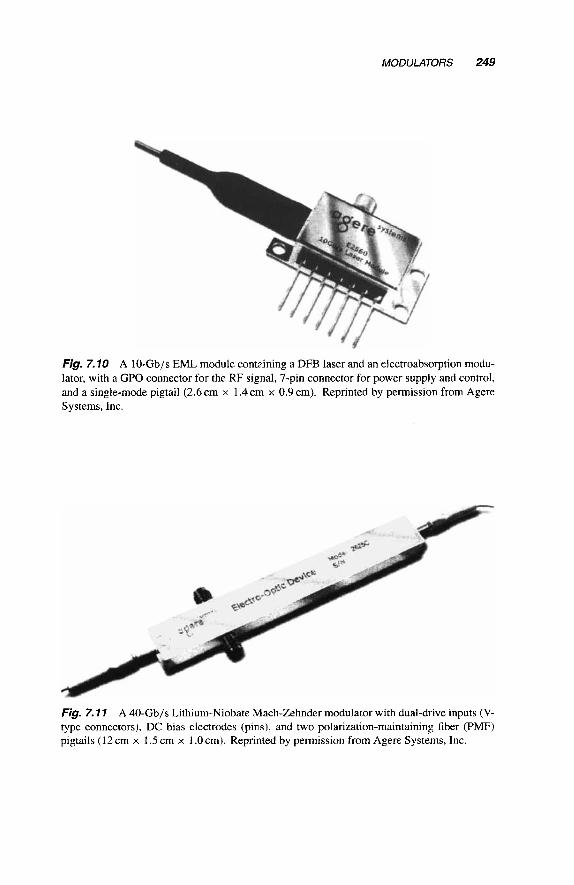
Fig. 7.10 A lO-Gb/s EML module containing a DFB laser and an electroabsorption modu- lator, with a GPO connector for the RF signal, 7-pin connector for power supply and control, and a single-mode pigtail (2.6 cm x 1.4 cm x 0.9 cm). Reprinted by permission from Agere Systems, Inc.
Fig. 7.11 A 4O-Gb/s Lithium-Niobate Mach-Zehnder modulator with dual-drive inputs (V- type connectors), DC bias electrodes (pinls), and two polarization-maintaining fiber (PMF) pigtails (12 cm x 1.5 cm x 1 .O cm). Reprinted by permission from Agere Systems, Inc.

250 OPTICAL TRANSMITTERS
DFB Laser EA Modulator
Light
Fig. 7.72 Integrated laser and electroabsorption modulator (schematically).
p0"t f k--------r + o r - - - , 1 \-iER* -- vMo 9 $,OR I VM __-_
0.1 ... 0.15 pF vs w
Fig. 7.73 (a) Switching curve and (b) electrical equivalent circuit of an electroabsorp- tion modulator.
all voltage and frequency conditions. At low frequencies, the nonlinear resistance degrades the matching, whereas at high frequencies, the shunt capacitance does the same thing. The accuracy of the matching usually is specified by the S11 parameter (cf. Appendix C).
Mach-Zehnder Modulator. Figure 7.14 (left) shows the top view of an MZ mod- ulator. The incoming optical signal is split equally and is sent down two different optical paths. After a few centimeters, the two paths recombine, causing the optical waves to interfere with each other. Such an arrangement is known as an interjerome- ter. If the phase shift between the two waves is O", then the interference is construetive and the light intensity at the output is high (on state); if the phase shift is 1 80°, then the interference is destructive and the light intensity is zero (off state). The phase shift, and thus the output intensity, is controlled by changing the delay through one or both of the optical paths by means of the electrooptic effect. This effect occurs in some materials such as lithium niobate (LiNbOs), some semiconductors, as well as some polymers and causes the refractive index to change in the presence of an electric field. Figure 7.14 (right) shows a cut view through an MZ modulator based on lithium niobate. Two RF waveguides in the form of coplanar transmission lines produce electrical fields, which penetrate into the two optical waveguides below. The latter are made from titanium (Ti) diffused into the lithium niobate substrate. Such a modulator also is known as a lithium-niobate modulator. [-+ Problem 7.51
The modulator shown in Fig. 7.14 is a so-called dual-drive MZM, because both light paths are controlled by two separate RF waveguides. Dual-drive MZMs, which have two input ports (also known as arms), can be driven in a push-pull fashion, which results in essentially zero optical chirp (more on this later). Another type of MZM controls both light paths with a single RF waveguide and thus is known as a

MODULATORS 257
Top view: Cut A-A: L = 3 - 4 crn 4 w RF waveguides - In fi-4 2 m + s i 0 2 LiNbO,
Optical waveguides A'
Fig- 7.74 Dual-drive Mach-Zehnder mo(du1ator based on LiNb03 (schematically).
single-drive MZM. The latter modulator requires only a single input signal, but in general is not chirp free.
Figure 7.15(a) shows the switching curve of an MZM, that is, the optical output power, Pout, as a function of the input voltage, V M , applied to the RF waveguide. (In the case of a dual-drive MZM, VIM represents the differential voltage between the two input ports.) Note that in contrast to the switching curve of the EAM, this curve is periodic rather than monotonic. The switching curve of an ideal MZM can be described by
(7.13)
where V, is the switching voltage. For VM = 0, 2V,, 4V,, and so forth, the output power is maximum (constructive interference) and for VM = V , , 3 V,, 5 V, , and so forth, the output power is zero (de;structive interference). Unfortunately, in real MZMs, delay mismatch between the two optical paths causes the switching curve to be shifted horizontally from its ideal position given by Eq. (7.13). Even worse, the horizontal shift is temperature and age dependent, causing the switching curve to drift. For this reason, MZMs typically require a bias controller that produces a bias voltage to compensate for this drift. The bias voltage can be added to the RF signal with a bias T; alternatively, some MZMs provide separate electrodes for the bias voltage besides the RF signal input [ 11.
fig. 7.75 (a) Switching curve and (b) electrical equivalent circuit of a Mach- Zehnder modulator.
The switching voltage, V,, typically is in the range of 4 to 6 V. A dual-drive MZM can be switched by applying $- V, / 2 and - V, / 2 to its two input ports, and thus requires a lower voltage swing per port than a single-drive MZM. The switching

252 OPTICAL TRANSMI7TERS
voltage of an MZM is inversely proportional to the length of the optical paths, L, that is, the product V, L is a constant. For example, given the typical value of 14 Vcm for this product [44], a modulator that is 14 cm long could be switched with a voltage of just 1 V. But such a long modulator would be very slow because the speed of an MZM depends inversely on its length L and the speed mismatch between the electrical and optical waves. For this reason, high-speed modulators are short and require a high switching voltage, making the driver design a formidable challenge.
From an electrical point of view, the MZM is just a transmission line (or, in the case of the dual-drive MZM, two transmission lines). The transmission line impedance typically is around 50 a, permitting the use of standard connectors and cables. The back-end of the transmission line usually is AC terminated within the package, as shown in Fig. 7.15(b).
The dynamic ER of a MZM is in the range of 15 to 17 dB and the chirp parameter can be made as low as < 0.1 [44]. In fact, with a dual-drive MZM, the chirp parameter can be controlled with the driving voltages. Assuming that the modulator is biased at the midpoint of the switching curve and that the two inputs ports are driven by synchronized signals having the same waveform shape, the chirp parameter turns out to be [4,44]
4% +e2 $1) - $1' f f =
M I M 2
(7.14)
where and GP2 are the (signed) voltage swings at the first and second input port, respectively. We can see that if the two input ports are driven in a push-pull fashion, 2' - -gP2, the chirp theoretically becomes zero. Furthermore, by choosing
small negative chirp, such as a = -0.5, causes optical pulses in a dispersive medium with D > 0 initially to compress, rather than expand,s leading to an extended reach. Finally, if both input ports are driven by the same signal, el = $L2, theoptical output signal is purely phase modulated with the intensity remaining constant (a -+ 00).
The capability of a dual-drive MZM to modulate the intensity as well as the phase makes it a very versatile device. One interesting use is the generation of a so-called optical duobinary signal. This signal has three levels: (i) light on with no phase shift, (ii) light off, and (iii) light on with 180" phase shift. This duobinary signal has the welcome property that its spectral linewidth is half that of a two-level NRZ signal, thus lowering the dispersion penalty. Yet, with proper precoding at the transmitter side, it can be received with a standard two-level intensity detector [206]. Other advanced modulation formats such as chirped return-to-zero (CRZ), carrier-suppressed return- to-zero (CS-RZ), and return-to-zero differential phase-shifi keying (RZ-DPSK) also can be generated with MZ modulators [64]. [+ Problem 7.61
The drawbacks of MZMs, besides the drift problem, the high switching voltage, and the bulky dimensions (see Fig. 7.1 l), are their rather high optical insertion loss (4-7 dB) and their sensitivity to the polarization of the optical signal.
u M l w - 4 -G2, v the chirp parameter of a dual-drive MZM can be made negative. A
5This effect is not described by our approximate Eqs. (2.6) and (7.2) and a more sophisticated theory is needed (e.g., see [51).

LIMITS IN OPTICAL COMMUNICATION SYSTEMS 253
7.4 LIMITS IN OPTICAL COMMUNICATION SYSTEMS
The following material is not required for the subsequent chapter on laser and mod- ulator driver design, but it is helpful for the understanding of optical transmission systems. By combining the transmitter linewidth equations of this chapter with the fiber properties discussed in Chapter 2 and the receiver sensitivity data of Chapter 5, we can now quantify all major limits in an optical communication system: (i) the lim- its due to chromatic dispersion, (ii) the limits due to polarization-mode dispersion, and (iii) the limits due to fiber attenuation.
Chromatic Dispersion Limits. For a transmitter that produces clean transform- limited pulses, for example, a DFB laser followed by a dual-drive MZM, we can approximate the maximum, dispersion-limited transmission distance by combining the spectral linewidth of Eq. (7.1) with the chromatic pulse-spreading expression of Eq. (2.6) and the spreading limit of Eq. (2.8) [46]:
(7.15)
However, because Eq. (2.6) is not precisely valid for transmitters with a narrow- linewidth source, such as a DFB laser, the above expression is only an approximation. A more precise analysis reveals that the attainable distances are longer than those given by Eq. (7.15), but the dependences on L) and B remain the same. A useful engineering rule states that to keep the dispersion penalty below 1 dB, we have to limit the distance to [73]
17 ps/(nm . km) 6,000 (Gb/s)2 km. (7.16)
For example, given an externally modulated 1.55-pm source without chirp transmit- ting over an SMF, we find from this rule that a 2.5-Gb/s system is limited to a span length of about 960km and a lO-Gb/s system to about 6 O l ~ n . ~ Note that the maxi- mum transmission distance diminishes rapidly with increasing bit rates, following a 1 / B2 law. This is so because the linewidth of a transform-limited transmitter increases with B (Eq. (7.1)), producing proportionally more pulse spreading (Eq. (2.6)), while at the same time the permitted amount of spreading decreases with B (Eq. (2.8)). So we are faced with two problems when going to higher bit rates and hence the 1 / B 2 dependence.
For a transmitter with a narrow-linewidth source that produces a significant amount of chirp, such as a directly modulated DFB laser, the dispersion-limited transmission distance can be approximated by combining Eq. (7.2) with Eqs. (2.6) and (2.8).
ID1 B 2 L i
62.S-Gb/s systems over more than 1.000krn and 10-Gb/s systems over more than 100 km can be realized if a dispersion penalty larger than 1 dB is tolerated, if a transmitter with prechirp optimization is used, or both.

254 OPTICAL TRANSMITTERS
Compared with Eq. (7.15), the maximum distance is reduced by d m :
(7.17)
Again, a more precise analysis finds a somewhat longer distance, but the dependences on a, D, and B remain the same. The following engineering rule is used often [73]:
L < - . km. (7.18)
For example, given a directly modulated 1.55-ym DFB laser with a = 4 transmitting over an SMF, we find that a 2.S-Gb/s system is limited to a span length of about 230km, and a lO-Gb/s system is limited to a span length of about 15 km.
For a transmitter with a wide-linewidth source, such as an FP laser or an LED, the dispersion-limited transmission distance can be found by combining Eq. (7.3) with Eqs. (2.6) and (2.8) [46]:
1 17 ps/(nm . km) 6,000 (Gb/sI2 - d m - ID1 B2
(7.19)
For example, given a 1.55-ym FP laser with a 3-nm linewidth transmitting over an SMF, we find that a 2.5-Gb/s system is limited to a span length of about 4 km and a lO-Gb/s system to about 1 km. Note that in Eq. (7.19), the transmission distance diminishes proportional to 1/B rather than to l / B 2 . This is so because in this case, the transmitter linewidth is not affected by the bit rate.
The numerical results of the examples are summarized in Table 7.1. The bit-rate dependence for all three examples (FP = Fabry-Perot laser with Ak = 3 nm, DFB = directly modulated DFB laser with a = 4, and EM = chirp-free external modulator) is plotted in Fig. 7.16. Note that all examples are based on a dispersion parameter of D = 17 ps/(nm . km) typical for a standard SMF operated at 1.55 pm. However, it is possible to reduce this value, and thus lengthen the transmission distances, by one of the following methods: (i) concatenate the SMF with a dispersion compensating fiber (DCF) to lower the overall dispersion, (ii) use a dispersion-shifted fiber (DSF) or nonzero dispersion-shifted fiber (NZ-DSF) instead of the SMF, or (iii) operate the .system at the 1.3-ym wavelength where dispersion in an SMF is lowest (but loss is higher).
Table 7.7 Maximum (unrepeatered) transmission distances over an SMF at 1.55 lLm for various transmitter types based on Eqs. (7.19), (7.18). and (7.16) with D = 17ps/(nm. km).
Transmitter Type 2.5 Gb/s lOGb/s
Fabry-Perot laser ( A h = 3 nm) 4 km 1 km Distributed feedback laser (a = 4) 230 km 15 km External modulator (a = 0) 960 km 60 km

LIMITS IN OPTICAL COMMUNICATION SYSTEMS 255
Fig. 7.16 Limits due to chromatic dispersion (FF', DFB, EM), polarization-mode dispersion (PMD, dashed), and attenuation (p-i-n, OA) in an SMFlink operated at the 1.55-pm wavelength.
PMD Limit. mode dispersion (PMD), Eq. (2.4), with the spreading limit tion 2.2), we find the PMD-limited transmission distance as
By combining the equa.tion for pulse spreading due to polarization- 5 O.l/B (cf. Sec-
(7.20)
For example, given the parameter DPMD = 0.1 ps/& typical for new PMD op- timized fiber, we find that a 2.5-Gb/s system is limited to a span length of about 160,000km and a 10-Gb/s system to about 10,OOOkm. These are huge spans ca- pable of connecting two continents! However, older, already-deployed fiber with DPMD = 2ps/& poses more serious limits: a 2.5-Gb/s system is limited to a span length of about 400km and a lO-Gb/s system to about 25 km. Note that these numbers are smaller than the dispersion-limited transmission distances for transform- limited pulses.
The bit-rate dependence of the PMD limit, for both values of the PMD parameter, is plotted in Fig. 7.16 with dashed lines.
Attenuation Limit. Given a transmitter launching the power FOut into the fiber and a receiver with the sensitivity Fsens, we easily can derive that fiber attenuation is limiting the transmission distance to [46]
(7.21)
where a is the fiber attenuation measured in dB/km. By expanding the log expression, we can rewrite this equation in the moire practical and intuitive form
- (7.22) Pout[d~mI - Psens~dBmI L ( -
a

256 OPTICAL TRANSMITTERS
For example, given a fiber attenuation of 0.25 dB/km, typical for an SMF operated at 1.55 pm, a launch power of 1 mW (OdBm), and a 10-Gb/s p-i-n detector with a sensitivity of -18.5 dBm, we find that the system is limited to a span length of 74 km. If we replace the p-i-n photodetector by an APD with the sensitivity of -27.0 dBm, this length increases to 108 km. Finally, for a receiver with an optically preamplified p-i-n detector that has a sensitivity of -36.0 dBm, the span length increases to 144 km.
The bit-rate dependence of the attenuation limit for a p-i-n receiver (p-i-n) as well as an optically preamplified p-i-n receiver (OA) is plotted in Fig. 7.16 based on the sensitivity data from Fig. 5.13. Note that this limit vanes much slower with bit rate than the other limits, which can be explained by the log function in Eq. (7.21). The curves in Fig. 7.16 are bases on a fiber attenuation of a = 0.25 dB/km; however, with the use of optical in-line amplifiers, the effective value of a can be reduced substantially, thus permitting much longer distances.
7.5 SUMMARY
Two types of modulation are used in optical transmitters:
0 Direct modulation, where the laser current is directly modulated by the signal.
0 External modulation, where the laser is always on and a subsequent optical modulator is used to modulate the laser light with the electrical signal.
In general, external modulation produces higher quality optical signals with a narrower spectral linewidth and a higher extinction ratio, but also is more costly and bulky than direct modulation.
The following light sources commonly are used in optical transmitters:
0 The Fabry-Perot (FP) laser, which is low in cost, but has a wide linewidth that severely limits the transmission distance in a dispersive fiber.
0 The distributed-feedback (DFB) laser, which has a very narrow linewidth and thus is an excellent continuous-wave (CW) source for external modulators. Even when modulated directly, the DFB laser has a fairly narrow linewidth (compared with CW operation, it is broadened because of chirp and the spec- trum of the modulation signal) and is suitable for long-reach systems.
0 The vertical-cavity surface-emitting laser (VCSEL), which is low in cost, mostly is used in data communication systems operating at short wavelengths.
0 The light-emitting diode (LED), which is very low in cost but has a very wide linewidth, low output power, and small modulation bandwidth, mostly is used for low-speed, short-reach data communication.
Electrically, all four sources are forward biased p-n junctions.

PROBLEMS 257
The following modulators commonly are used in optical transmitters:
The electroabsorption modulator (EAM), which is small and can be driven with a reasonably small voltage swing. Electrically, it is a reverse-biased p-n junction.
The Mach-Zehnder modulator (MZM), which generates the highest-quality optical pulses with a controlled amount of chirp and a high extinction ratio. Electrically, it is a (terminated) transmission line.
The maximum transmission distance that can be achieved in an optical communi- cation system is determined by a combination of the chromatic dispersion limit, the polarization-mode dispersion (PMD) limit, and the attenuation limit.
7.6
7.1
7.2
7.3
7.4
7.5
7.6
PROBLEMS
Power Penalty due to Finite Extinction Ratio. Derive the power penalty caused by a transmitter with a finite extinction ratio. (a) Assume the noise at the receiver is signal independeint. (b) Assume the rms noise current at the receiver is proportional to the square root of the signal current.
Laser Materials. Photodetectors for both the 1.3- and 1.55-pm wavelengths can use the same InGaAs material for the absorption layer. Why do lasers for the 1.3- and 1.55-pm wavelengths require two different InGaAsP compounds for the active layer?
Chirp Parameter. The chirp parameter a sometimes is defined as
m / a t o(t) := 2 P ( t ) . -
aP/at’ (7.23)
where @ is the phase and P is the intensity of the electromagnetic field. Show how this definition relates to Eq. (7.10).
Power Penalty due to RIN Noise. Derive the power penalty caused by the laser RIN noise in a transmission system with a p-i-n receiver. Assume a DC- balanced NRZ signal with high extinction and a signal-independent receiver noise, i;,amp, in addition to the RLTN noise.
Power Conservation in a Mach-Zehnder Modulator. The MZM uses con- structive and destructive interference to modulate the laser light. In the case of destructive interference, light power goes into the modulator but no light power comes out of it. Where does the power go?
Duobinary Modulation. An NFZ signal with bit rate B is processed (filtered) by adding a delayed copy of the signal to itself. The delay is one bit period or l / B . (a) How many levels does the resulting signal have? (b) What is the transfer function H ( f ) of the “delay and add” function? (c) What is the spectrum of the resulting duobinary signal?
-