
Optical surveillance on silicon chips: your crypto keys ...sps32/SG_talk_OSSC_a.pdf · –...
36
Optical surveillance on silicon chips: your crypto keys are visible Security Group, Computer Laboratory, University of Cambridge, 13 October 2009 Optical surveillance on silicon chips: your crypto keys are visible Dr Sergei Skorobogatov http://www.cl.cam.ac.uk/~sps32 email: [email protected]
-
Upload
truongquynh -
Category
Documents
-
view
217 -
download
0
Transcript of Optical surveillance on silicon chips: your crypto keys ...sps32/SG_talk_OSSC_a.pdf · –...

Optical surveillance on silicon chips: your crypto keys are visible Security Group, Computer Laboratory, University of Cambridge, 13 October 2009
Optical surveillance on silicon chips: your crypto keys are visible
Dr Sergei Skorobogatovhttp://www.cl.cam.ac.uk/~sps32 email: [email protected]
2
Optical surveillance on silicon chips: your crypto keys are visible Security Group, Computer Laboratory, University of Cambridge, 13 October 2009
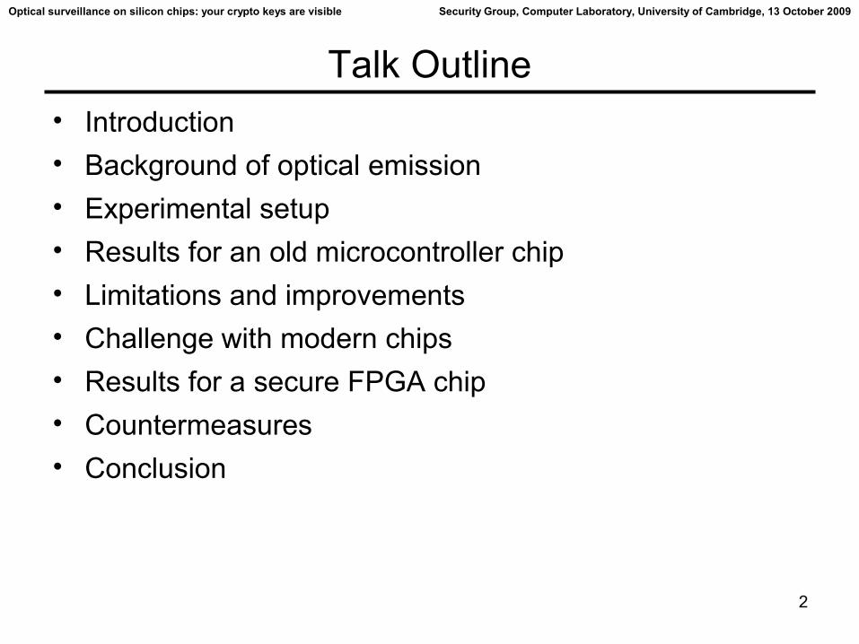
Talk Outline• Introduction• Background of optical emission• Experimental setup• Results for an old microcontroller chip• Limitations and improvements• Challenge with modern chips• Results for a secure FPGA chip• Countermeasures• Conclusion

3
Optical surveillance on silicon chips: your crypto keys are visible Security Group, Computer Laboratory, University of Cambridge, 13 October 2009
Introduction• Operating semiconductor circuits emit photons
– known for over 40 years– actively used in failure analysis for over 20 years
• Existing failure analysis techniques– picosecond imaging circuit analysis (PICA) uses photomultiplier
array– photon emission microscopy (PEM) uses special IR cameras– both techniques are expensive and require sophisticated sample
preparation• What about hardware security?
– any possibility of seeing internal signals?– any leaks from memory arrays?

4
Optical surveillance on silicon chips: your crypto keys are visible Security Group, Computer Laboratory, University of Cambridge, 13 October 2009
Introduction• Optical emission analysis attacks were introduced in 2008
and exploit well known fact that photon emission of a chip is correlated with the processed data*– done on a PIC16F84A (0.9 μm) running at 6MHz with 7V supply– from backside with the silicon substrate thinned down to 20 μm– using Mepsicron II camera with hi-res 2D imaging and 50ps timing– continued for 12 hours with test code in a loop– proved that AES key can be extracted from the operating device
• Can this be used to compromise security in silicon chips?– requires expensive equipment and special chip preparation– was not considered as a threat, hence, no protection is in place– does not form part of standard security evaluation techniques
* J. Ferrigno et al, “When AES blinks: introducing optical side channel”, IET Information Security

5
Optical surveillance on silicon chips: your crypto keys are visible Security Group, Computer Laboratory, University of Cambridge, 13 October 2009
Introduction• Challenges
– find low-cost detectors suitable for optical emission analysis– reduce the cost of sample preparation
• Any technical progress for the past 20 years?– are modern CCD cameras good for the attack?– what about photomultipliers (PMT)?– what parameters are essential for such detectors?
• If optical emission from operating chip has correlation with processed data, is there any correlation between photon emission and power consumption?– if found, this can be used for finding weak spots in protection
against power analysis attacks– optical emission can be scaled down to an individual transistor

6
Optical surveillance on silicon chips: your crypto keys are visible Security Group, Computer Laboratory, University of Cambridge, 13 October 2009
Background• What is the problem with optical emission analysis attacks?• Number of photons emitted per every switch of a transistor
Ne = SeB(LHId/qvs)Ts ~ 10−2...10−4 photons/switchSe – spectral emission density, B – emission bandwidth, LH – hot-carrier region length,Id – drain current, q – e− charge, vs – carrier saturated velocity, Ts – transition time
• Emission spectrum is from ~500nm to above 1200nm with maximum emission at 900nm…1100nm (NIR region)
• Small fraction of emitted photons can be detected: <1%– emission is isotropic, so with a lens only 25%…45% is observed– there are losses in optics due to reflections and absorption (80%)– low quantum efficiency (QE) of detectors in NIR region: 1%…20%
• Backside approach: <0.1%– high refractive index of silicon (n1000nm=3.58) causes high reflection
(32%) and low critical angle (θ=16.2º) results in reduced aperture

7
Optical surveillance on silicon chips: your crypto keys are visible Security Group, Computer Laboratory, University of Cambridge, 13 October 2009
Background• Optical emission is higher from the n-MOS transistor due
to higher mobility of electrons• Emission takes place near the drain area where the
speed of carriers declines
8
Optical surveillance on silicon chips: your crypto keys are visible Security Group, Computer Laboratory, University of Cambridge, 13 October 2009
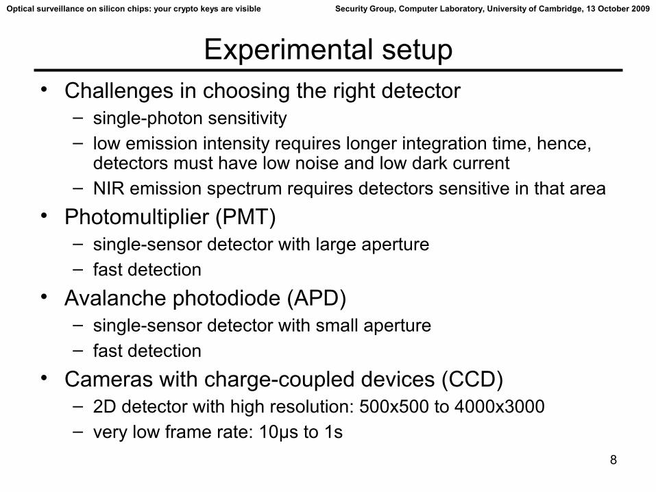
Experimental setup• Challenges in choosing the right detector
– single-photon sensitivity– low emission intensity requires longer integration time, hence,
detectors must have low noise and low dark current– NIR emission spectrum requires detectors sensitive in that area
• Photomultiplier (PMT)– single-sensor detector with large aperture– fast detection
• Avalanche photodiode (APD)– single-sensor detector with small aperture– fast detection
• Cameras with charge-coupled devices (CCD)– 2D detector with high resolution: 500x500 to 4000x3000– very low frame rate: 10μs to 1s

9
Optical surveillance on silicon chips: your crypto keys are visible Security Group, Computer Laboratory, University of Cambridge, 13 October 2009
Experimental setup• Challenges in choosing the right PMT and APD: as good
as possible NIR sensitivity, as low as possible dark current– PMT usually have very limited NIR sensitivity– detectors with better NIR sensitivity have higher dark current– low dark current in APD is caused by their small aperture size– too small aperture size of APD (10μm…500μm) complicates their
usage
200ps501%2%400–1100Sensl PCDMini-0020
780ps4000%0%250–850Hamamatsu H6780-01
900ps20002%2%850–1250Hamamatsu H10330-25
50ps0.0050%1%180–940Quantar Mepsicron II, S25
Time responseDark current, e−/s
QE at 1000nm
QE at 900nm
Wavelength, nm
Type of detector

10
Optical surveillance on silicon chips: your crypto keys are visible Security Group, Computer Laboratory, University of Cambridge, 13 October 2009
Experimental setup• Challenges in choosing the right CCD camera: as good as
possible NIR sensitivity, as low as possible dark current– monochrome cameras have good NIR sensitivity– CCTV and hobbyist astronomical cameras have low dark current
and good NIR sensitivity
10μs0.025%12%300–1100Sony EXview HAD CCD
10μs0.021%8%300–1050Sony Super HAD CCD
20ms10%0%400–700Average colour CCD
20ms11%5%400–1000Average monochrome CCD
20ms0.0110%30%200–1100Hamamatsu C4880-50
20ms0.320%50%200–1200Hamamatsu C4880-21
50ps0.0050%1%180–940Quantar Mepsicron II, S25
Time responseDark current, e−/s
QE at 1000nm
QE at 900nm
Wavelength, nm
Type of detector

11
Optical surveillance on silicon chips: your crypto keys are visible Security Group, Computer Laboratory, University of Cambridge, 13 October 2009
Experimental setup• Sample preparation: PIC16F628 microcontroller (0.9μm)• Locating internal blocks: Flash, EEPROM, SRAM, CPU• Running the chip at 20MHz clock (5MIPS) with 6V power
supply to boost the emission

12
Optical surveillance on silicon chips: your crypto keys are visible Security Group, Computer Laboratory, University of Cambridge, 13 October 2009
Experimental setup• PMT setup: decapsulated chip facing sensor's aperture
– Hamamatsu H6780-01 PMT sensor
• CCD setup: camera mounted on a microscope with the chip placed in a test socket– Starlight Xpress SXV-H9 CCD camera
13
Optical surveillance on silicon chips: your crypto keys are visible Security Group, Computer Laboratory, University of Cambridge, 13 October 2009
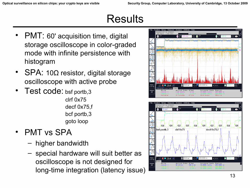
Results• PMT: 60' acquisition time, digital
storage oscilloscope in color-graded mode with infinite persistence with histogram
• SPA: 10Ω resistor, digital storage oscilloscope with active probe
• Test code: bsf portb,3clrf 0x75decf 0x75,fbcf portb,3goto loop
• PMT vs SPA– higher bandwidth– special hardware will suit better as
oscilloscope is not designed for long-time integration (latency issue)

14
Optical surveillance on silicon chips: your crypto keys are visible Security Group, Computer Laboratory, University of Cambridge, 13 October 2009
Results• PMT vs SPA
– higher bandwidth provides more data for analysis– possible localisation of source through apertures and optics– good correlation suggests possibility of using optical emission
analysis for characterisation of areas contributing to power trace– acquisition of emission requires some time with the device under
test performing the same operation and precisely synchronised
15
Optical surveillance on silicon chips: your crypto keys are visible Security Group, Computer Laboratory, University of Cambridge, 13 October 2009
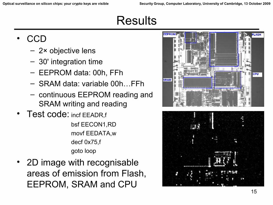
Results• CCD
– 2× objective lens– 30' integration time– EEPROM data: 00h, FFh– SRAM data: variable 00h…FFh– continuous EEPROM reading and
SRAM writing and reading• Test code: incf EEADR,f
bsf EECON1,RDmovf EEDATA,wdecf 0x75,fgoto loop
• 2D image with recognisable areas of emission from Flash, EEPROM, SRAM and CPU

16
Optical surveillance on silicon chips: your crypto keys are visible Security Group, Computer Laboratory, University of Cambridge, 13 October 2009
Results• CCD with high magnification
– 100× objective lens– 10' integration time– EEPROM data: 00h, FFh– continuous EEPROM reading
• Test code: incf EEADR,fbsf EECON1,RDmovf EEDATA,wgoto loop
• Emission from the NMOS transistor is significantly higher than from the PMOS

17
Optical surveillance on silicon chips: your crypto keys are visible Security Group, Computer Laboratory, University of Cambridge, 13 October 2009
Results• EEPROM area
– 10× objective lens– 10' integration time– data: 56h, 56h, 56h…56h, 00h– continuous EEPROM reading
• Test code: incf EEADR,fbsf EECON1,RDmovf EEDATA,wgoto loop
• Flash memory has similar structure and gives similar result– data extraction is complicated by
the fact that program code is executed from the flash memory

18
Optical surveillance on silicon chips: your crypto keys are visible Security Group, Computer Laboratory, University of Cambridge, 13 October 2009
Results• SRAM area
– 10× objective lens– 10' integration time– data: A6h, W=A6h– continuous reading and writing
• Test code: movf 0x75, w movwf 0x75goto loop goto loop
• Low emission from memory cells– write drivers, bus drivers, row and
column selectors leak the most• Write data have the same
emission for ‘0’ and ‘1’– dual-rail logic used in SRAM:
separate bit lines for writing ‘0’ & ‘1’– difference in the emission could
predict leakage in the power trace

19
Optical surveillance on silicon chips: your crypto keys are visible Security Group, Computer Laboratory, University of Cambridge, 13 October 2009
Results• SRAM area
– 10× objective lens– 10' integration time– data: A6h, W=C3h– continuous XOR operation
• Test code: movlw 0xA6movwf 0x74movlw 0xC3xorwf 0x74, fgoto loop
• Leakage through both read and write logic– read: intensity is proportional to the
number of ‘1’s– write: ‘0’s and ‘1’s are separated
20
Optical surveillance on silicon chips: your crypto keys are visible Security Group, Computer Laboratory, University of Cambridge, 13 October 2009
Limitations and improvements• Data recovery
– slow process: minimum 1 minute per byte
• Modern chips– three or more metal layers prevent direct observation and analysis– smaller technologies will require longer integration time
• Backside approach– silicon is transparent to light with wavelengths above 1000 nm– lower spatial resolution of ~1μm (R=0.61λ/NA)– longer integration time due to higher losses in silicon and optics– higher magnification lenses give better result– use of NIR optics improves result, but expensive– substrate thinning and AR coating are useful, but expensive– increase of the power supply voltage boosts the optical emission

21
Optical surveillance on silicon chips: your crypto keys are visible Security Group, Computer Laboratory, University of Cambridge, 13 October 2009
Limitations and improvements• Increasing the power supply voltage: every 10% of
increase above nominal voltage boosts the emission by 40%…120%
• PIC16F628: EEPROM reading
43026232928400242712861046Photometry results
6.0V5.5V5.0V4.5V4.0V3.5VPower supply voltage

22
Optical surveillance on silicon chips: your crypto keys are visible Security Group, Computer Laboratory, University of Cambridge, 13 October 2009
Limitations and improvements• PIC16F628 (0.9μm) vs PIC16F628A (0.5μm):
higher density with CMP technology: approx. 5 times lower intensity

23
Optical surveillance on silicon chips: your crypto keys are visible Security Group, Computer Laboratory, University of Cambridge, 13 October 2009
Limitations and improvements• PIC16F628: EEPROM area from front and rear sides
higher reflections and absorption in Si: approx. 10 times lower intensity

24
Optical surveillance on silicon chips: your crypto keys are visible Security Group, Computer Laboratory, University of Cambridge, 13 October 2009
New challenges• Actel® ProASIC3® 0.13μm, 7 metal layers, flash FPGA
– “highly secure FPGA” which is reprogrammable, non-volatile, single-chip and live-at-power-up solution
– “offer one of the highest levels of design security in the industry”– robust design security features: flash logic array, flash ROM,
security fuses, FlashLock™, AES– “even without any security measures (such as FlashLock with
AES), it is not possible to read back the programming data from a programmed device”
– allows secure ISP field upgrades using 128-bit AES-encrypted bitstream with AES authentication and MAC verification
– other security measures: voltage monitors, internal charge pumps, asynchronous internal clock and many others
– “unique in being highly resistant to both invasive and noninvasive attacks”

25
Optical surveillance on silicon chips: your crypto keys are visible Security Group, Computer Laboratory, University of Cambridge, 13 October 2009
Experimental setup• Sample preparation of A3P060 FPGA: front and rear
– the surface is covered with sticky polymer which needs to be removed for physical access to the surface
– >99% of the surface is covered with supply grid or dummy fillers– backside: low-cost approach used – without any treatment

26
Optical surveillance on silicon chips: your crypto keys are visible Security Group, Computer Laboratory, University of Cambridge, 13 October 2009
Experimental setup• Sample preparation: front
– only three top metal layers are visible at a most
– full imaging will require de-layering and scanning electron microscopy
– any invasive attacks will require sophisticated and expensive equipment
27
Optical surveillance on silicon chips: your crypto keys are visible Security Group, Computer Laboratory, University of Cambridge, 13 October 2009
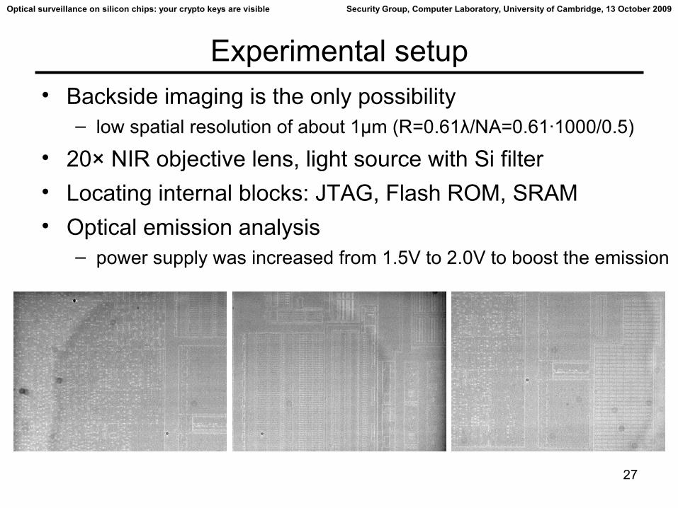
Experimental setup• Backside imaging is the only possibility
– low spatial resolution of about 1μm (R=0.61λ/NA=0.61·1000/0.5)
• 20× NIR objective lens, light source with Si filter• Locating internal blocks: JTAG, Flash ROM, SRAM• Optical emission analysis
– power supply was increased from 1.5V to 2.0V to boost the emission

28
Optical surveillance on silicon chips: your crypto keys are visible Security Group, Computer Laboratory, University of Cambridge, 13 October 2009
Experimental setup• Increasing the power supply voltage: every 10% of increase
above nominal Vcc boosts the emission by 40%…120%• A3P060: JTAG ID reading
232709536527019531194889Photometry results
2.5V2.2V2.0V1.8V1.6V1.5VPower supply voltage

29
Optical surveillance on silicon chips: your crypto keys are visible Security Group, Computer Laboratory, University of Cambridge, 13 October 2009
Results• JTAG glue logic
– 20× NIR objective lens, 60' integration time
– repeating the same operation• Some recognisable differences• Partial reverse engineering – information
– operation-related activity– obfuscated data flow paths– security-related operations

30
Optical surveillance on silicon chips: your crypto keys are visible Security Group, Computer Laboratory, University of Cambridge, 13 October 2009
Results• Flash ROM (Settings + Data)
– 20× NIR objective lens– 60' integration time– continuous reading
• Recognisable data pattern– some data can be extracted– gives information about location

31
Optical surveillance on silicon chips: your crypto keys are visible Security Group, Computer Laboratory, University of Cambridge, 13 October 2009
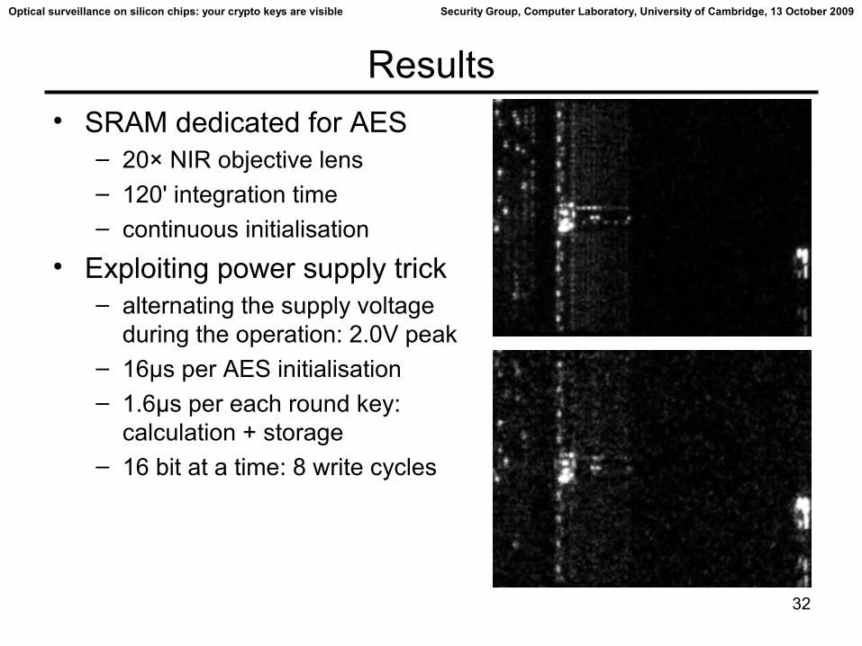
Results• SRAM dedicated for AES
– 20× NIR objective lens– 120' integration time– continuous initialisation
• AES key recovery– key scheduling used in AES– AES key can be easily calculated
from any round key– existence of separate JTAG
commands for AES initialisation, authentication and decryption
– information is leaked by the SRAM array and write drivers
32
Optical surveillance on silicon chips: your crypto keys are visible Security Group, Computer Laboratory, University of Cambridge, 13 October 2009
Results• SRAM dedicated for AES
– 20× NIR objective lens– 120' integration time– continuous initialisation
• Exploiting power supply trick– alternating the supply voltage
during the operation: 2.0V peak– 16μs per AES initialisation– 1.6μs per each round key:
calculation + storage– 16 bit at a time: 8 write cycles

33
Optical surveillance on silicon chips: your crypto keys are visible Security Group, Computer Laboratory, University of Cambridge, 13 October 2009
Results• SRAM dedicated for AES
– 20× NIR objective lens– 120' integration time– continuous initialisation
• Exploiting power supply trick– alternating the supply voltage during
the last round operation: 2.5V peak– 0.2μs increase of the supply voltage
from 1.5V to 2.5V for one write cycle
34
Optical surveillance on silicon chips: your crypto keys are visible Security Group, Computer Laboratory, University of Cambridge, 13 October 2009
Countermeasures• Use of modern chips with multiple metal layers forces an
attacker to use backside approach and results in longer time required for the attack
• Metal shielding over sensitive areas can help but cannot prevent backside analysis
• Adding dummy cycles to normal operations• Encryption makes analysis harder• Asynchronous circuits could make the attack more
problematic as data analysis requires synchronisation

35
Optical surveillance on silicon chips: your crypto keys are visible Security Group, Computer Laboratory, University of Cambridge, 13 October 2009
Conclusion• Optical emission analysis can be carried out at a relatively low cost
using hobbyist astronomical CCD cameras with low-magnification optics
• Long exposure time is required: the device must perform the same operation millions of times in a loop
• PMT offers high bandwidth and acquired data have correlation with power analysis results and can be used for finding weak spots in protection against power analysis attacks
• Optical emission analysis offers possibility for partial reverse engineering of chips including data analysis
• Backside approach can help in modern chips, but has lower spatial resolution and requires longer integration time
• Increase of the power supply voltage boosts the optical emission and considerably reduces the time of analysis
• Modern deep-submicron chips do leak information through optical emission when their power supply is increased by at least 30%
• Lack of protection against optical side-channel attacks in modern chips might lead to possible vulnerabilities

36
Optical surveillance on silicon chips: your crypto keys are visible Security Group, Computer Laboratory, University of Cambridge, 13 October 2009
Further reading• J. Ferrigno, M. Hlaváč, “When AES blinks: introducing optical side
channel”, IET Information Security, Vol. 2, No. 3, 2008, pp. 94–98• S. Skorobogatov, “Using Optical Emission Analysis for Estimating
Contribution to Power Analysis”, 6th Workshop on Fault Diagnosis and Tolerance in Cryptography (FDTC 2009), 06 September 2009, Lausanne, Switzerland. IEEE-CS Press, ISBN 978-0-7695-3824-2, pp.111–119
• Up-to-date information: http://www.cl.cam.ac.uk/~sps32/