
Optical Properties of Semiconductor-Metal Hybrid...
62
Jakob Philipp Ebner Optical Properties of Semiconductor-Metal Hybrid Nanoparticles Diplomarbeit zur Erlangung des akademischen Grades eines Magisters an der Naturwissenschaftlichen Fakult¨ at der Karl-Franzens-Universit¨ at Graz Betreuer: Ao. Univ. Prof. Mag. Dr. Ulrich Hohenester Institut f¨ ur Physik Fachbereich Theoretische Physik 2013
Transcript of Optical Properties of Semiconductor-Metal Hybrid...
Jakob Philipp Ebner
Optical Properties ofSemiconductor-Metal Hybrid
Nanoparticles
Diplomarbeit
zur Erlangung des akademischen Grades einesMagisters
an der Naturwissenschaftlichen Fakultat derKarl-Franzens-Universitat Graz
Betreuer: Ao. Univ. Prof. Mag. Dr. Ulrich Hohenester
Institut fur PhysikFachbereich Theoretische Physik
2013
Contents
1. Introduction 11.1. Prologue . . . . . . . . . . . . . . . . . . . . . . . . . . . . . . . . 11.2. Structure of this thesis . . . . . . . . . . . . . . . . . . . . . . . . 3
2. Basic Principles 42.1. Electromagnetic fields . . . . . . . . . . . . . . . . . . . . . . . . 4
2.1.1. Direct Coulomb interaction . . . . . . . . . . . . . . . . . 42.1.2. Maxwell’s equations . . . . . . . . . . . . . . . . . . . . . 62.1.3. Quasistatic approximation . . . . . . . . . . . . . . . . . . 7
2.2. Plasmons . . . . . . . . . . . . . . . . . . . . . . . . . . . . . . . 82.2.1. Dielectric function of metals . . . . . . . . . . . . . . . . . 92.2.2. Surface Plasmons . . . . . . . . . . . . . . . . . . . . . . . 102.2.3. Particle Plasmons . . . . . . . . . . . . . . . . . . . . . . . 13
2.3. Semiconductors . . . . . . . . . . . . . . . . . . . . . . . . . . . . 142.3.1. Excitons . . . . . . . . . . . . . . . . . . . . . . . . . . . . 142.3.2. Effective Mass . . . . . . . . . . . . . . . . . . . . . . . . . 152.3.3. Interband Polarization . . . . . . . . . . . . . . . . . . . . 16
2.4. Nano and Quantum optics . . . . . . . . . . . . . . . . . . . . . . 172.4.1. Dipole Approximation . . . . . . . . . . . . . . . . . . . . 182.4.2. Rotating Wave Approximation . . . . . . . . . . . . . . . . 182.4.3. Cross sections . . . . . . . . . . . . . . . . . . . . . . . . . 19
3. Theory 223.1. Describing the System . . . . . . . . . . . . . . . . . . . . . . . . 223.2. Polarization . . . . . . . . . . . . . . . . . . . . . . . . . . . . . . 243.3. Optical response . . . . . . . . . . . . . . . . . . . . . . . . . . . 26
4. Numerics 304.1. Discretizing the Hamiltonian . . . . . . . . . . . . . . . . . . . . . 304.2. Boundary Element Method . . . . . . . . . . . . . . . . . . . . . . 30
4.2.1. BEM theory . . . . . . . . . . . . . . . . . . . . . . . . . . 314.2.2. Surface discretization . . . . . . . . . . . . . . . . . . . . . 32
4.3. Program outline . . . . . . . . . . . . . . . . . . . . . . . . . . . . 33
i
Contents
5. Results 355.1. Combining Particles . . . . . . . . . . . . . . . . . . . . . . . . . 365.2. Charge carrier densities . . . . . . . . . . . . . . . . . . . . . . . . 375.3. Polarization . . . . . . . . . . . . . . . . . . . . . . . . . . . . . . 395.4. Optical response . . . . . . . . . . . . . . . . . . . . . . . . . . . 415.5. Influence of numerical parameters . . . . . . . . . . . . . . . . . . 43
5.5.1. Grid size . . . . . . . . . . . . . . . . . . . . . . . . . . . . 435.5.2. Number of states . . . . . . . . . . . . . . . . . . . . . . . 44
5.6. Problems . . . . . . . . . . . . . . . . . . . . . . . . . . . . . . . . 445.7. Conclusion . . . . . . . . . . . . . . . . . . . . . . . . . . . . . . . 44
Acknowledgements 46
A. Calculations 47A.1. Boundary Conditions . . . . . . . . . . . . . . . . . . . . . . . . . 47A.2. Potentials in media . . . . . . . . . . . . . . . . . . . . . . . . . . 49A.3. Exciton wave functions . . . . . . . . . . . . . . . . . . . . . . . . 51
B. Conventions and Conversions 53B.1. Atomic Units . . . . . . . . . . . . . . . . . . . . . . . . . . . . . 53B.2. Gaussian-CGS Units . . . . . . . . . . . . . . . . . . . . . . . . . 54B.3. Energy conversion . . . . . . . . . . . . . . . . . . . . . . . . . . . 54
Bibliography 56
ii

Abstract
In this thesis I study the optical properties of a hybrid nanoparticle consisting
of a metal and a semiconductor part. I examine the electrostatic influence of
the metallic particle on the exciton states. Further, I calculate the effect of the
semiconductor on the plasmon that is optically created on the metal surface. I
derive a framework to calculate the polarization of the semiconductor due to the
external and plasmonic fields, and use it to obtain the scattering and absorption
spectra for the combined particle.
I treat a model system where the semiconductor is approximated by a few mate-
rial specific parameters and the geometry is a match stick shaped structure with
a semiconducting rod and a metallic tip. For our simulations I use the MNPBEM
[1] toolbox for Matlab, which uses the boundary element method [2] for the cal-
culation of electromagnetic potentials.
I find that the optical response of the combined particle is enhanced with respect
to the response of separated particles. Exciton resonances are shifted to lower
energies in the presence of a metal and the exciton-dipole self interaction via the
environment appears to have very little effect on the optical properties.
iii
1. Introduction
1.1. Prologue
Particles whose dimensions do not exceed the nanometer scale at least in one
dimension are called nanoparticles. They live at the boundary of the quantum
and the classical world, small enough to exhibit quantum mechanical behaviour
but still consisting of thousands to millions of atoms. Since great progress has been
made in manufacturing such small particles, many new effects can be studied and
new applications can be found in this area.
A very interesting feature of metallic nanoparticles, that was even used in Roman
times, is the occurrence of particle plasmons. These are oscillations of electrons
in a metal that can be driven by an electromagnetic wave. They exhibit optical
properties strongly depending on the size and geometry of the particles, and not
only on the material, as common pigments do. The ancient example for particle
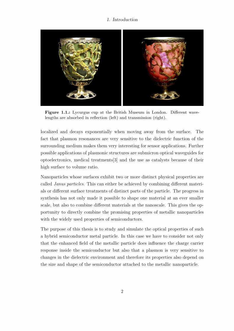
plasmons mentioned above is the Lycurgus cup (Fig. 1.1) which appears to have
different colors depending on the direction of illumination. It appears green if
lighted from the front but looks red if illuminated from the back or from inside.
This behaviour comes from different resonance properties of plasmons in light
absorption and scattering. In the first case one sees the reflected light, and in
the second case one sees the light after specific frequencies are absorbed. This
technique, namely adding tiny portions of gold and silver nanoparticles to the
glass, was also used in more “recent” history for colorful church windows where
normal dyes would have dissolved long ago.
A very important feature for the application of plasmons is the occurrence of a
very strong electric field at the metallic surface that can be several magnitudes
stronger than the exciting light field. This so called evanescent field is strongly
1
1. Introduction
Figure 1.1.: Lycurgus cup at the British Museum in London. Different wave-lengths are absorbed in reflection (left) and transmission (right).
localized and decays exponentially when moving away from the surface. The
fact that plasmon resonances are very sensitive to the dielectric function of the
surrounding medium makes them very interesting for sensor applications. Further
possible applications of plasmonic structures are submicron optical waveguides for
optoelectronics, medical treatments[3] and the use as catalysts because of their
high surface to volume ratio.
Nanoparticles whose surfaces exhibit two or more distinct physical properties are
called Janus particles. This can either be achieved by combining different materi-
als or different surface treatments of distinct parts of the particle. The progress in
synthesis has not only made it possible to shape one material at an ever smaller
scale, but also to combine different materials at the nanoscale. This gives the op-
portunity to directly combine the promising properties of metallic nanoparticles
with the widely used properties of semiconductors.
The purpose of this thesis is to study and simulate the optical properties of such
a hybrid semiconductor metal particle. In this case we have to consider not only
that the enhanced field of the metallic particle does influence the charge carrier
response inside the semiconductor but also that a plasmon is very sensitive to
changes in the dielectric environment and therefore its properties also depend on
the size and shape of the semiconductor attached to the metallic nanoparticle.
2
1. Introduction
In particular, we are interested in the influence of the exciton excitations on the
optical properties of the system. In this thesis we treat a matchstick shaped
structure consisting of a semiconductor nanorod with an attached gold sphere,
which is dissolved in toluene, as an example for such a system.
1.2. Structure of this thesis
After this introduction we summarize some textbook knowledge that is necessary
for our further investigations in chapter 2. Chapter 3 will show our theoretical
approach to the systems Hamiltonian and the optical response. In chapter 4 we
translate our findings of chapter 3 into a numerical scheme. Our final results will
be presented in chapter 5 where we will compare the behaviour of the combined
particles to its components and show its scattering and absorption cross sections.
Some auxiliary calculations can be found in Appendix A.
Throughout the theory part we use Hartree atomic units and CGS units (Appendix
B). The results are presented in milli-electron Volts (meV) and nanometers (nm).
Operators are not emphasized explicitely but should be recognizable as such.
3
2. Basic Principles
In this chapter we will gather some textbook results of the topics that are crucial
for the understanding of this thesis. Most of them will only be touched briefly,
but further references will be given in each section.
2.1. Electromagnetic fields
In this section we will give a short overview of some aspects of classical electrody-
namics following references [4] and [5]. We remind you that all formulas will be
in the cgs unit system.
2.1.1. Direct Coulomb interaction
Electrostatics is based on Coulomb’s law, which was discovered in the second half
of the 18th century and first published by Charles Auguste de Coulomb [6]. It
describes the vectorial force of an arbitrary charge distribution ρ(r′) on a charge
q at position r in vacuum
F = q
∫ρ(r′)
(r− r′)
|r− r′|3dτ ′. (2.1)
The concept to describe electrostatics and electrodynamics in modern physics, is
with fields and potentials
Φ(r) =
∫ρ(r′)
|r− r′|dτ ′. (2.2)
4
2. Basic Principles
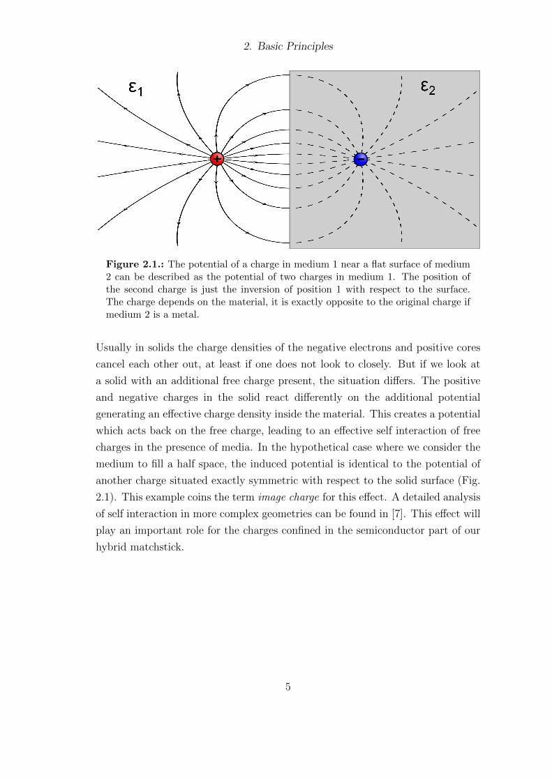
Figure 2.1.: The potential of a charge in medium 1 near a flat surface of medium2 can be described as the potential of two charges in medium 1. The position ofthe second charge is just the inversion of position 1 with respect to the surface.The charge depends on the material, it is exactly opposite to the original charge ifmedium 2 is a metal.
Usually in solids the charge densities of the negative electrons and positive cores
cancel each other out, at least if one does not look to closely. But if we look at
a solid with an additional free charge present, the situation differs. The positive
and negative charges in the solid react differently on the additional potential
generating an effective charge density inside the material. This creates a potential
which acts back on the free charge, leading to an effective self interaction of free
charges in the presence of media. In the hypothetical case where we consider the
medium to fill a half space, the induced potential is identical to the potential of
another charge situated exactly symmetric with respect to the solid surface (Fig.
2.1). This example coins the term image charge for this effect. A detailed analysis
of self interaction in more complex geometries can be found in [7]. This effect will
play an important role for the charges confined in the semiconductor part of our
hybrid matchstick.
5
2. Basic Principles
2.1.2. Maxwell’s equations
Between 1861 and 1865 Clark Maxwell cast the whole knowledge about electro-
dynamics in dielectric media into the four following equations [8]
∇ · D(r, t) = 4πρ(r, t), (2.3a)
∇ · B(r, t) = 0, (2.3b)
∇×H(r, t) =4π
cj(r, t) +
1
c
∂D(r, t)
∂t, (2.3c)
∇× E(r, t) = −1
c
∂B(r, t)
∂t. (2.3d)
Where D is the dielectric displacement, E the electric field, B and H are the
magnetic induction and magnetic field and ρ and j are the free charge and current
densities. In isotropic linear media the dielectric displacement simply reads D =
εE and the magnetic fields are related via B = µH. ε is the permittivity which
we assume constant in space, for each medium, throughout this thesis. µ is the
magnetic permeability which can be set to one at optical frequencies.
From these four equations we deduce that the electric and magnetic fields are not
independent. Indeed they can be rewritten in form of the scalar potential φ and
the magnetic vector potential A as
E = −∇φ− 1
c
∂
∂tA, B = ∇×A . (2.4)
One can easily see that the potentials automatically fulfill the homogeneous Maxwell
equations (2.3b) and (2.3d). But these definitions do not uniquely define the po-
tentials and leave a so called freedom of gauge. To reduce these redundancies one
can introduce conditions on the potentials that may simplify the problem at hand.
We want to derive wave equations for the potentials and therefore introduce the
Lorentz condition
6
2. Basic Principles
∇ · A +ε1
c
∂
∂tφ = 0. (2.5)
If we consider harmonic electromagnetic waves with a time dependence e−iωt and
the wave vector k = ω/c the time derivative simplifies to ∂/∂t = −iω and we can
deduce from (2.3a)
∇ · E = ∇ · (−∇φ+ ikA) = −∇2φ+ ik∇A = 4πρ
ε. (2.6)
In combination with the Lorenz condition this gives
∇2φ+ k2εφ = −4πρ
ε. (2.7)
By starting from (2.3c) we can analogously derive a similar equation for the vector
potential
∇2 A +k2εA = −4π
cj. (2.8)
These equations are called the Helmholtz equations for potentials and are equiva-
lent to Maxwell’s equations.
2.1.3. Quasistatic approximation
If we examine a particle much smaller than the light wavelength we can neglect
retardation effects and assume the electromagnetic field constant throughout the
particle. Thus, we set k ≈ 0 which leads to a vanishing vector potential A
in Lorentz gauge (2.5) and the Helmholtz equation of the scalar potential (2.7)
simplifies to the Poisson equation
∇2Φ = −4πρ
ε. (2.9)
For the homogeneous case, in which no free charges are present, this results in the
Laplace equation
7
2. Basic Principles
∇2φ = 0. (2.10)
For the solution of the Poisson equation we can employ the Green’s function
formalism. Green’s functions are a well established tool to solve inhomogeneous
differential equations. The inhomogeneous part of a differential equation can be
solved with the help of such a Green’s function which is defined as a solution of
D G(r, r′) = −4πδ(r, r′). (2.11)
For the Poisson equation, D = ∇2, in a homogeneous unbound medium there
exists a relatively simple solution to this problem. The so-called electrostatic
Green’s function
G(r, r′) =1
ε|r− r′|, (2.12)
where the factor 1/ε, which appears on the right hand side of (2.9), is already
incorporated into the Green’s function. With this Green’s function we can write
the solution of the Poisson equation (2.9) as φ(r) =∫G(r, r′, ε)ρ(r′)dr′ plus any
function that satisfies the Laplace equation (2.10).
Thus, in homogeneous media where ε is constant inside the medium, we can
transform the volume integral into a surface integral using Gauss’s theorem and
write the solution for the potential in the ad-hoc form [2, 9]
φ(r) = φext(r) +
∮G(r, s)σ(s)da. (2.13)
2.2. Plasmons
Plasmons are the quasiparticles of quantized collective oscillations of the free elec-
tron gas in solids, similar to phonons, the quasiparticles of vibrations. They can
be divided into bulk plasmons, surface plasmons and particle plasmons. Bulk plas-
mons, which are e.g. responsible for the shiny appearance of metals, are situated
8
2. Basic Principles
throughout the whole volume of a solid, surface plasmons are located at interfaces
between a metal and a dielectric, and particle plasmons occur at metallic particles
which are smaller than the light wavelength.
The topics treated in this section are discussed in more detail in [10] and [11].
2.2.1. Dielectric function of metals
A simple, but very effective, way to describe the response of a metal to an applied
electric field is the Drude-Sommerfeld theory. The free electron gas is treated in
a classical kinetic fashion, and a damped harmonic oscillator is obtained for the
equation of motion
m∂2r
∂t2+mγ
∂r
∂t= eE0 e
−iωt, (2.14)
where γ is a material specific damping term, m and e are the mass and charge of
an electron respectively, E0 is the amplitude and ω the frequency of the external
electric field. With the ansatz r = r0e−iωt we can derive the polarization of the
metal and therefore get the dielectric function in Drude form
ε(ω) = 1−ω2p
ω2 + iγω, (2.15)
where ωp is the bulk plasma frequency that depends on the electron density in the
corresponding metal. If we assume a negligible damping we can conclude that the
refractive index n =√ε becomes strictly imaginary and light can not penetrate
the metal very far if the exciting frequency ω is smaller than ωp.
What the formulas above do not take into account is that electrons can absorb
the energy of the electric field to be excited into a higher band. This leads to a
breakdown of the theory around and above the transition energies, for gold this
is the case for wavelengths around 550 nm. There exist theoretical approaches
to include these interband transitions [11], but in this thesis we use experimental
values for the dielectric functions [12].
9
2. Basic Principles
2.2.2. Surface Plasmons
In this section we will discuss plasmons located at an interface between a metal
and a dielectric. We will derive the necessary requirements for the existence of
such a plasmon. Therefore we will start by applying Maxwell’s equations to such
an interface.
We already know that the Helmholtz equation (2.7) follows directly from
Maxwell’s equations in a source free environment, and in terms of the dielectric
function it looks like
(∇2 + ε(r, ω)
ω2
c2
)E(r, ω) = 0 (2.16)
If we look at a flat interface perpendicular to the z-axis at z=0, we can describe
the environment with the dielectric function
ε(r, ω) =
ε1(ω), if z > 0,
ε2(ω), if z < 0,(2.17)
with ε1 being positive and therefore representing a dielectric, while ε2 is negative
and corresponds to the metal. If we split the electric field into a transversal
electric (TE) and a transversal magnetic (TM) mode one can show that there is
no solution to the Helmholtz equation in the TE case [11]. Therefore we will now
take a closer look at the TM mode, where the electric fields in the media are
Ej = Ej,x
1
0
−kx/kj,z
ei(kxx+kj,zz−ωt), (2.18)
where j is the index to the respective medium. Because the parallel component
of the wave vector is conserved at the interface, we get the condition
k2x + k2j,z = εjk2. (2.19)
10
2. Basic Principles
Since we do not consider free charges in our current examination we find from
(2.3a) that
kxEj,x + kj,zEj,z = 0. (2.20)
Inserting this into (2.18) we arrive at
Ej = Ej,x
1
0
−kx/kj,z
ei(kxx+kj,zz−ωt). (2.21)
The surface plasmons also have to obey the boundary conditions for the electric
field (section A.1):
E1,x − E2,x = 0,
ε1E1,z − ε2E2,z = 0. (2.22)
If we want to satisfy equations (2.20) and (2.22) we arrive at two alternatives.
The first one is kx = 0, where clearly no wave is propagating along the surface.
The second possibility is
ε1k2,z − ε2k1,z = 0. (2.23)
Together with (2.20) this yields the following dispersion relations
k2x =ε1ε2ε1 + ε2
k2 =ε1ε2ε1 + ε2
ω2
c2, (2.24)
k2j,z =ε2j
ε1 + ε2k2. (2.25)
Since we are interested in a propagating wave in x-direction we require a real kx,
which imposes certain relations on the dielectric functions. If we look at (2.24) we
11
2. Basic Principles
see that the product and the sum of the dielectric functions need to have the same
sign. Furthermore, we demand an imaginary kz because we want waves localized
at the surface and not propagating into the media. This gives for the dielectric
functions
ε1(ω) · ε2(ω) < 0, (2.26)
ε1(ω) + ε2(ω) < 0. (2.27)
These relations are fulfilled if we combine a metal which has a negative dielectric
function with a dielectric which usually has a positive dielectric function smaller
than that of the metal.
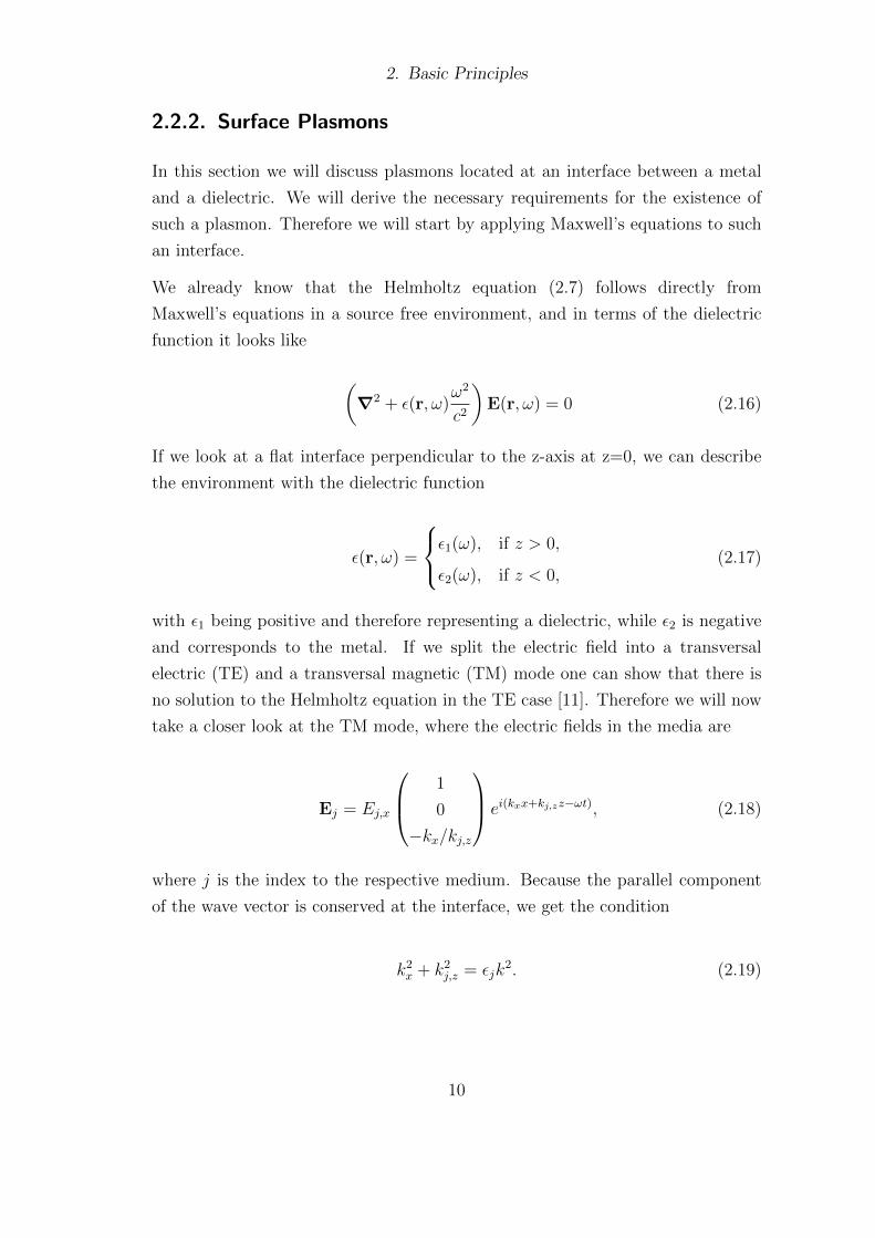
Figure 2.2.: Dispersion relation of a surface plasmon. Here we assume a surfacebetween vacuum and metal. The dispersion relation of light in vacuum (yellowsolid line) does not cross the dispersion relation of the surface plasmon (red). Anincoming wave in the dielectric (yellow dashed) crosses the red line and and asurface plasmon with this frequency can be excited (source: [13]).
In Fig. 2.2 the dispersion relation of the surface plasmon is plotted together with
that of light in the dielectric ω = kxc/nd. We see that no surface plasmon can
be excited by such an electromagnetic wave because the lines of the dispersion
relations do not cross, which means, that energy-momentum conservation can not
12
2. Basic Principles
εg
εm
εb εmεb
a) b)
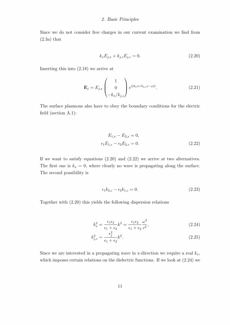
εg
Figure 2.3.: Excitation of surface plasmon. If the dielectric of the prism is higherthan that of the background total can occur and the dispersion in the prism is lesssteep than in the background. The evanescent field of the totally reflected wavein the prism has the same dispersion relation as the wave itself, therefore it canexcite a surface plasmon at the interface between background and metal. For a)the Otto geometry it is difficult to keep the distance constant whereas for b) theKretschmann-Raether geometry the thickness of the metal film has to be smallerthan the skin depth of the evanescent field.
be fulfilled. A solution to achieve such an excitation is to “tilt” the light line by
slowing down the exciting light. This means that the light has to come in through
an optically thicker medium than the dielectric along which the surface plasmon
propagates. This can be accomplished in the Kretschmann-Raether geometry [14]
or the Otto geometry [15] which are shown in Fig. 2.3.
2.2.3. Particle Plasmons
If we turn from a planar interface to a metallic nanoparticle that is smaller than
the exciting wavelength we do not have propagating waves but localized plasmons.
The free electron gas in the metal gets polarized and the ionic background exhibits
a restoring force. Thus the particle acts as an oscillator whose resonance not only
depends on the properties of the involved media but is also strongly influenced by
the geometry and size of the particle.
13
2. Basic Principles
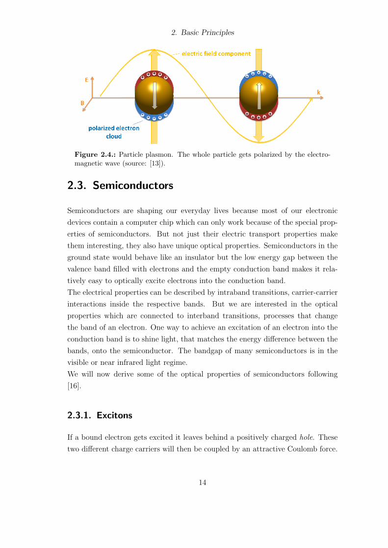
Figure 2.4.: Particle plasmon. The whole particle gets polarized by the electro-magnetic wave (source: [13]).
2.3. Semiconductors
Semiconductors are shaping our everyday lives because most of our electronic
devices contain a computer chip which can only work because of the special prop-
erties of semiconductors. But not just their electric transport properties make
them interesting, they also have unique optical properties. Semiconductors in the
ground state would behave like an insulator but the low energy gap between the
valence band filled with electrons and the empty conduction band makes it rela-
tively easy to optically excite electrons into the conduction band.
The electrical properties can be described by intraband transitions, carrier-carrier
interactions inside the respective bands. But we are interested in the optical
properties which are connected to interband transitions, processes that change
the band of an electron. One way to achieve an excitation of an electron into the
conduction band is to shine light, that matches the energy difference between the
bands, onto the semiconductor. The bandgap of many semiconductors is in the
visible or near infrared light regime.
We will now derive some of the optical properties of semiconductors following
[16].
2.3.1. Excitons
If a bound electron gets excited it leaves behind a positively charged hole. These
two different charge carriers will then be coupled by an attractive Coulomb force.
14
2. Basic Principles
This can be described quantum mechanically through a quasiparticle called exci-
ton. We can distinguish two limiting cases - strongly bound Frenkel excitons and
loosely bound Wannier or Wannier-Mott excitons. Frenkel excitons are created
in materials where the Coulomb interaction is strong between electron and hole.
This is the case in materials with a low dielectric constant and can e.g. be found
in organic semiconductor crystals. In inorganic semiconductors we usually have a
high dielectric constant and the interaction between the charges is screened, lead-
ing to Wannier-Mott excitons. The binding energy of a Wannier-Mott exciton is
only a few meV in contrast to a Frenkel exciton which can have binding energies
up to several hundred meV.
2.3.2. Effective Mass
With quantum mechanics we can calculate the equation of motion for an electron
in a crystal with an applied electric field E as
d2r
dt2=
1
h2d2E(k)
dk2qE, (2.28)
where E(k) is the energy as function of the wavenumber of the electron [17]. If we
compare this with the equation of motion for a free electron in an electric field
d2r
dt2=
1
mqE, (2.29)
we see that we can describe the electron in the crystal as a free electron with a
modified mass
m∗ =
(1
h2d2E(k)
dk2
)−1, (2.30)
which is called the effective mass of the electron.
Since any smooth function can be approximated by a parabola near a local ex-
tremum and the second derivative of a parabola is constant we can assume a
constant effective mass for our charge carriers. This assumption is justified be-
cause any excess energy that a hole or electron might have directly after the
excitation will be transferred to the crystal lattice. This process happens rapidly
compared to the lifetime of the exciton, and therefore the exciton will spend most
15
2. Basic Principles
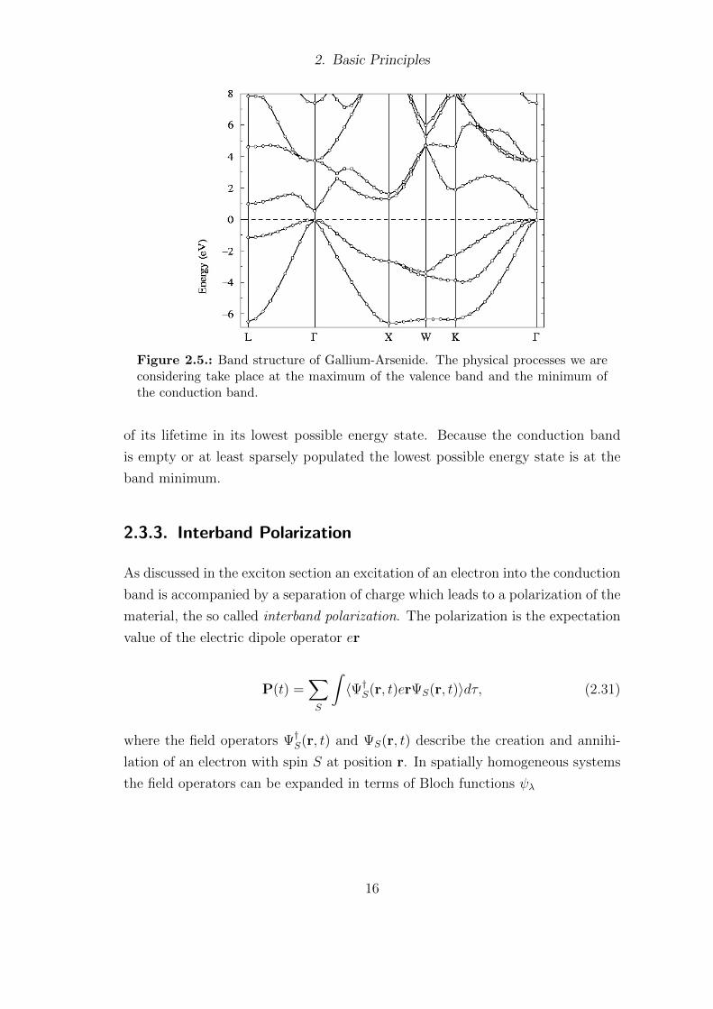
Figure 2.5.: Band structure of Gallium-Arsenide. The physical processes we areconsidering take place at the maximum of the valence band and the minimum ofthe conduction band.
of its lifetime in its lowest possible energy state. Because the conduction band
is empty or at least sparsely populated the lowest possible energy state is at the
band minimum.
2.3.3. Interband Polarization
As discussed in the exciton section an excitation of an electron into the conduction
band is accompanied by a separation of charge which leads to a polarization of the
material, the so called interband polarization. The polarization is the expectation
value of the electric dipole operator er
P(t) =∑S
∫〈Ψ†S(r, t)erΨS(r, t)〉dτ, (2.31)
where the field operators Ψ†S(r, t) and ΨS(r, t) describe the creation and annihi-
lation of an electron with spin S at position r. In spatially homogeneous systems
the field operators can be expanded in terms of Bloch functions ψλ
16
2. Basic Principles
ΨS(r, t) =∑λ,k
aλ,k,S(t)ψλ(k, r), (2.32)
where λ is the band index. Inserting this into (2.31) we get
P(t) =∑
λ,λ′,k,k′
〈a†λ,kaλ′,k′〉∫ψ∗λ,k(r)erψλ′,k′(r)dτ, (2.33)
where we incorporated the spin index into the summation over k. The integral
over the Bloch functions can be calculated generally[16] and gives
∫ψ∗λ,k(r)erψλ′,k′(r)dτ = δk,k′dλλ′ , (2.34)
with the dipole moment dλ,λ′ that is associated with the respective interband tran-
sition. We restrict our treatment to the transition between valence and conduction
band and get for the interband polarization
P(t) =∑k
〈a†c,kav,k〉dcv + c.c. . (2.35)
2.4. Nano and Quantum optics
Applying quantum mechanics to optical phenomena led to many new insights
and applications during the last century, the most prominent certainly being the
invention of the laser. A fully quantum mechanical approach would require to
quantize the particles and the electromagnetic fields. In this thesis we choose a
semi classical approach where we treat the exciton as a quantum emitter but do
not quantize the radiating field. Textbooks that discuss quantum optics are e.g.
[18] and [16].
17
2. Basic Principles
2.4.1. Dipole Approximation
Typically the size of an atom is small compared to the wavelengths of the light
that performs the transitions between different atomic energy levels. Thus the
variation of the electric field over the extent of the atom almost does not vary. So
we have k · r 1 and we can expand the electric field in a power series
E(r, t) = E(t)e−ik · r = E(t)(1− ik · r + ...) (2.36)
and only take the leading term of the expansion. This is known as the electric
dipole approximation.
Taking only the leading term is equivalent to neglecting the momentum of the
photon, k→ 0, especially in comparison to the electron momentum. This means
that only vertical transitions are allowed in a band diagram like Fig. 2.5.
2.4.2. Rotating Wave Approximation
If we consider an optical two level system with the frequency ω corresponding to
the transition between the states driven by an electrical field
E(t) = E0 e−iωt + E∗0 e
iωt, (2.37)
the interaction Hamiltonian within the dipole approximation is Hop = −d · E,
where d is the dipole moment of the transition between the states. Therefore we
can write the interaction Hamiltonian for a two state system as
Hop = −(|2〉 〈1|d21 + |1〉 〈2|d∗21)(E0 e−iωt + E∗0 e
iωt) (2.38)
where we used d12 = d∗21. If we transform this Hamilton in the interaction picture
with the transformation U = eiH0t = eiω0t|2〉〈2|, we obtain
18
2. Basic Principles
Hop,I = UHopU† =− |2〉 〈1| (d · E0 e
−i(ω−ω0)t + d · E∗0 ei(ω+ω0)t)
− |1〉 〈2| (d∗ · E0 e−i(ω+ω0)t + d∗ · E∗0 ei(ω−ω0)t).
(2.39)
If the frequency of the electric field is near the resonance, the terms with (ω−ω0)
become nearly time independent, whereas the counter rotating terms (ω+ω0) os-
cillate rapidly and average out to zero on the timescales we are interested in. If we
neglect these fast oscillating terms we arrive at the rotating wave approximation
Hop,I = − |2〉 〈1|Ωe−i(ω−ω0)t − |1〉 〈2|Ω∗ei(ω−ω0)t, (2.40)
with Ω = d · E0 being the Rabi frequency.
2.4.3. Cross sections
This section deals with the absorption and scattering cross sections for nanopar-
ticles. It mainly follows the derivations in [19].
We define the scattering cross section as the power of the scattered electromagnetic
field integrated over a sphere around the scattering particle divided by the power
of the incoming field. The energy flux of an electromagnetic wave is given by the
Poynting vector
S =c
4πE×B, (2.41)
which points in the propagation direction of the wave. For a plane wave the time
average of its magnitude is given by
〈S〉 =c
8πE2 . (2.42)
This quantity is also called intensity.
If we apply a field E0 to a particle it induces induces a dipole moment d
d = αE0 . (2.43)
19
2. Basic Principles
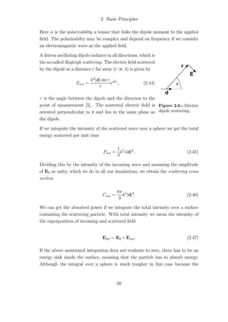
Here α is the polarizability a tensor that links the dipole moment to the applied
field. The polarizabilty may be complex and depend on frequency if we consider
an electromagnetic wave as the applied field.
γ
d
r
E
Figure 2.6.: Electricdipole scattering.
A driven oscillating dipole radiates in all directions, which is
the so-called Rayleigh scattering. The electric field scattered
by the dipole at a distance r far away (r λ) is given by
Esca =k2|d| sin γ
reikr, (2.44)
γ is the angle between the dipole and the direction to the
point of measurement [5]. The scattered electric field is
oriented perpendicular to r and lies in the same plane as
the dipole.
If we integrate the intensity of the scattered wave over a sphere we get the total
energy scattered per unit time
Psca =1
3k4c|d|2. (2.45)
Dividing this by the intensity of the incoming wave and assuming the amplitude
of E0 as unity, which we do in all our simulations, we obtain the scattering cross
section
Csca =8π
3k4|d|2. (2.46)
We can get the absorbed power if we integrate the total intensity over a surface
containing the scattering particle. With total intensity we mean the intensity of
the superposition of incoming and scattered field
Etot = E0 + Esca . (2.47)
If the above mentioned integration does not evaluate to zero, there has to be an
energy sink inside the surface, meaning that the particle has to absorb energy.
Although the integral over a sphere is much tougher in this case because the
20
2. Basic Principles
electric field is not radially symmetric we can derive the absorption cross section
similar to the scattering cross section and arrive at
Cabs = 4πk Im(e ·d), (2.48)
where e is the unit vector in direction of the incoming field.
We have now summarized the main ingredients for the derivations and simulations
that will follow in the next chapters.
21
3. Theory
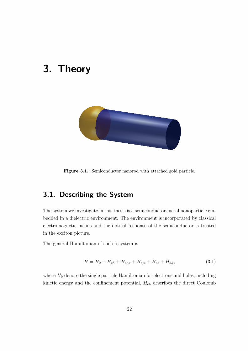
Figure 3.1.: Semiconductor nanorod with attached gold particle.
3.1. Describing the System
The system we investigate in this thesis is a semiconductor-metal nanoparticle em-
bedded in a dielectric environment. The environment is incorporated by classical
electromagnetic means and the optical response of the semiconductor is treated
in the exciton picture.
The general Hamiltonian of such a system is
H = H0 +Heh +Henv +Hopt +Hee +Hhh, (3.1)
where H0 denote the single particle Hamiltonian for electrons and holes, including
kinetic energy and the confinement potential, Heh describes the direct Coulomb
22
3. Theory
interaction between electron and hole, Henv incorporates the Coulomb coupling
to the dielectric environment and Hopt accounts for optical creation of excitons.
Hee and Hhh describe the electron-electron and hole-hole interaction, respectively,
but we assume a low density of excitons and therefore neglect these interactions
in linear response.
In the two band approximation we consider only one electron and and one hole
band. Thus we can write H0 in terms of the field operators Ψ†i (r) and Ψi(r), which
create/annihilate an electron or a hole at position r, as
H0 =∑i=e,h
∫Ψ†i (r)
(− ∇
2
2mi
+ Vi(r)
)Ψi(r)dτ, (3.2)
where mi denotes the effective mass of an electron or hole in the semiconductor.
The Coulomb term becomes
Heh = −∫∫
G0(r, r′)ne(r)nh(r
′)dτdτ ′, (3.3)
where the ni = Ψ†i (r)Ψi(r) are the electron and hole particle densities and
G0(r, r′) = 1/(ε|r−r′|) is the electrostatic Green’s function in an unbound medium.
To describe the optical interaction with an external field we use dipole approxi-
mation and rotating wave approximation, this leads from (2.40) to
Hop = −∫
Ω(r)Ψ†e(r)Ψ†h(r) + Ω(r)∗Ψe(r)Ψh(r) dτ. (3.4)
Here Ω(r) = d · E+(r) is the Rabi energy, with d the dipole moment associated
with the interband transition and E+ the external electric field with positive
frequency components. The only part that is left now is the interaction with the
environment which we describe through the bound charges ρb which are induced
due to the free charge density ρf of electrons and holes. Then this interaction can
be written in the form
23
3. Theory
Henv =
∫∫G0(r, r
′)ρf (r)ρb(r′)dτdτ ′
=
∫∫G0(r, r
′)(Ψ†hΨh −Ψ†eΨe)ρb(r′)dτdτ ′.
(3.5)
For the Hop and Henv we will see a strong influence of the metallic nanoparticle
compared to the bare semiconductor. In the environment part the bound charges
will be much stronger because the electrons are free within the metal and the
optical response will be enhanced due to the field magnification of the particle
plasmons.
3.2. Polarization
In a semiconductor electrons and holes are always created pairwise by incident
light. Thus, if we assume that in the ground state there are no electrons in the
conduction band and the valence band is completely filled, one can show that
every n-point function An, normal ordered with respect to the exciton-picture, is
at least of order m in the electric field [20]. Here m = max(ne, nh) where ne and
nh are the number of electron and hole field operators in the n-point function.
In this thesis we consider the linear response in the electric field therefore the
only density matrix we have to treat is the 2-point function interband polarization
p(r, r′) = 〈Ψh(r)Ψe(r′)〉. All density matrices of higher order in the electric field
will be discarded.
To obtain the equation of motion for the interband polarization we use the Heisen-
berg equation of motion
d
dtp = − i
h[p,H] , (3.6)
the square bracket denoting the commutator of the two operators.
24
3. Theory
To get the commutators of the field operators with the Hamiltonian we use the
anti-commutation relations of fermionic field operators, see for example [21],
Ψi(r),Ψ†j(r′) = δijδ(r− r′) (3.7)
Ψi(r)†,Ψj(r′)† = Ψi(r),Ψj(r
′) = 0 (3.8)
(i = e, h), and the fact that we can discard all operators which consist of more
than one field operator of the same type after normal ordering. Thereby we get
[Ψe(r), H0] =
(− ∇
2
2me
+ Ve(r)
)Ψe(r), (3.9)
[Ψe(r), Heh] = −∫G0(r, r
′)ρhΨe(r)dτ ′, (3.10)
[Ψe(r), Henv] = −∫G0(r, r
′)ρbΨe(r)dτ ′, (3.11)
[Ψe(r), Hop] = −Ω(r)Ψ†h(r). (3.12)
The commutation relations for the hole operators are analog, just the sign in
the equations with Henv and Hop changes. After using the product relation for
commutators
[AB,C] = A[B,C] + [A,C]B, (3.13)
we can arrange the field operators in normal order and then neglect again all the
terms that correspond to O(E2). Hence we obtain
id
dtp =
(− ∇
2e
2me
+ Ve(re)−∇2h
2mh
+ Vh(rh)−G0(re, rh)
)p(re, rh)
−∫
(G0(re, r)−G0(rh, r))〈Ψh(rh)ρb(r)Ψe(re)〉dτ − 〈Ψh(rh)Ψ†h(rh)〉Ω(re, t).
(3.14)
From (3.7) it follows that the last term is simply δ(re − rh)Ω(re, t). The second
term describes the coupling to the environment. In the integral we can replace
25
3. Theory
(see section A.2)
G0ρb = (G
ε−G0)ρf = (
G
ε−G0)(−Ψ†eΨe + Ψ†hΨh), (3.15)
where G is the full electrostatic Green’s function incorporating the geometry of
the media. After invoking the commutation relations again we can finally write
down the equation of motion for the polarization in the linear field limit
id
dtp(re, rh) =
(− ∇
2e
2me
+ Ve(re)−∇2h
2mh
+ Vh(rh)−G(re, rh)
ε
)p(re, rh)
− δ(re − rh)Ω(re, t).
(3.16)
3.3. Optical response
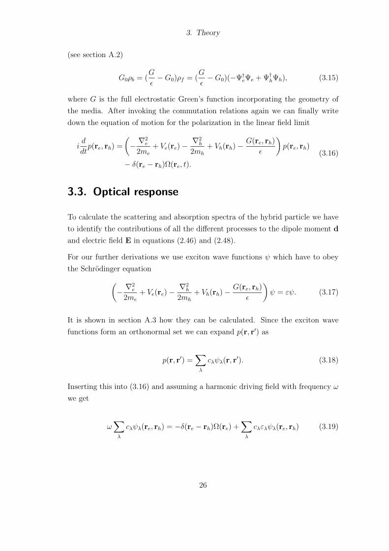
To calculate the scattering and absorption spectra of the hybrid particle we have
to identify the contributions of all the different processes to the dipole moment d
and electric field E in equations (2.46) and (2.48).
For our further derivations we use exciton wave functions ψ which have to obey
the Schrodinger equation(− ∇
2e
2me
+ Ve(re)−∇2h
2mh
+ Vh(rh)−G(re, rh)
ε
)ψ = εψ. (3.17)
It is shown in section A.3 how they can be calculated. Since the exciton wave
functions form an orthonormal set we can expand p(r, r′) as
p(r, r′) =∑λ
cλψλ(r, r′). (3.18)
Inserting this into (3.16) and assuming a harmonic driving field with frequency ω
we get
ω∑λ
cλψλ(re, rh) = −δ(re − rh)Ω(re) +∑λ
cλελψλ(re, rh) (3.19)
26
3. Theory
Einc
Eref
Eexc
dsurf
dexc
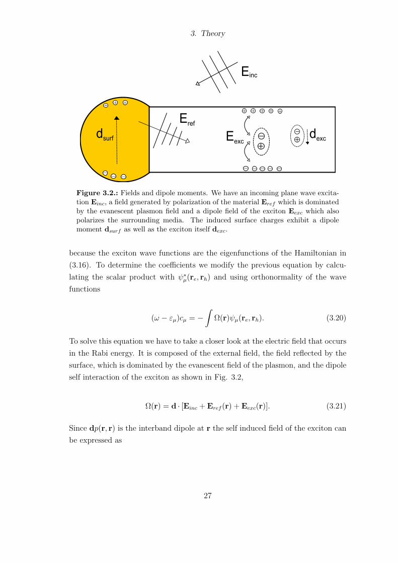
Figure 3.2.: Fields and dipole moments. We have an incoming plane wave excita-tion Einc, a field generated by polarization of the material Eref which is dominatedby the evanescent plasmon field and a dipole field of the exciton Eexc which alsopolarizes the surrounding media. The induced surface charges exhibit a dipolemoment dsurf as well as the exciton itself dexc.
because the exciton wave functions are the eigenfunctions of the Hamiltonian in
(3.16). To determine the coefficients we modify the previous equation by calcu-
lating the scalar product with ψ∗µ(re, rh) and using orthonormality of the wave
functions
(ω − εµ)cµ = −∫
Ω(r)ψµ(re, rh). (3.20)
To solve this equation we have to take a closer look at the electric field that occurs
in the Rabi energy. It is composed of the external field, the field reflected by the
surface, which is dominated by the evanescent field of the plasmon, and the dipole
self interaction of the exciton as shown in Fig. 3.2,
Ω(r) = d · [Einc + Eref (r) + Eexc(r)]. (3.21)
Since dp(r, r) is the interband dipole at r the self induced field of the exciton can
be expressed as
27
3. Theory
Eexc(r) = k2∫ ←→
G (r, r′)d∑µ
cµψµ(r′, r′)dτ , (3.22)
where←→G (r, r′) is the dyadic Green’s function that relates a dipole at r′ to its
reflected field at r via the environment, which lets us define the term
Kµµ′ = k2∫ψµ(r, r) d(r) ·
←→G (r, r′) ·d(r′) ψµ′(r
′, r′)dτdτ ′. (3.23)
Together with the additional substitution
Ωµ =
∫d · [Einc + Eref (r)]ψµ(r, r)dτ (3.24)
we can rewrite (3.20) as
(ω − εµ)cµ = −Ωµ −∑µ′
Kµµ′c′µ, (3.25)
which gives a set of linear equations that are easy to solve numerically.
We do not only have to split up the electric field but also have to consider what
the involved dipoles, that interact with those fields, are. First of all we consider
the dipole moment exhibited by the surface charge of the particle
dsurf =
∫∂V
σ(s)s da =
∫∂V
[σinc(s) + σexc(s)]s da, (3.26)
where σinc is the surface charge induced by the incoming electric field, selfconsis-
tently incorporating the reflected field of the metallic nanoparticle, and σexc is the
surface charge generated by the exciton. The other dipole moment we consider is
that of the exciton, i.e. the integral over the polarization
dexc =∑µ
∫d cµψµ(r, r) dτ. (3.27)
We now have all the ingredients needed to calculate the spectra of the particle:
28
3. Theory
Csca =8π
3k4 |dsurf + dexc|2 (3.28)
and
Cabs ∝ ImEinc ·dsurf +∑µ
cµ
∫ψµ(r, r)d · [Einc + Eref (r)+Eexc(r)]dτ. (3.29)
If we take a closer look at the integral in the absorption cross section we see that
it is the same as the right hand side of (3.20) except for the sign. We can therefore
write a simpler expression
Cabs = 4πk ImEinc ·dsurf −∑µ
c2µ(ω − εµ). (3.30)
With these results we conclude this chapter and go on to show the numerical
means we used to calculate the quantities which occurred in our derivations so
far.
29
4. Numerics
Solving Maxwell’s equations and calculating the Green’s functions is not possible
for arbitrary particle geometries and we have to resort to numerics to treat our
system. This chapter will give an overview of the used numerical techniques. All
computations and the visualizations were done in Matlab with excessive use of
the MNPBEM toolbox [1]. This is a toolbox to simulate metallic nanoparticles
with the boundary element method which we will explain shortly. Other methods
of solving Maxwell’s equations may be found in [22], for example.
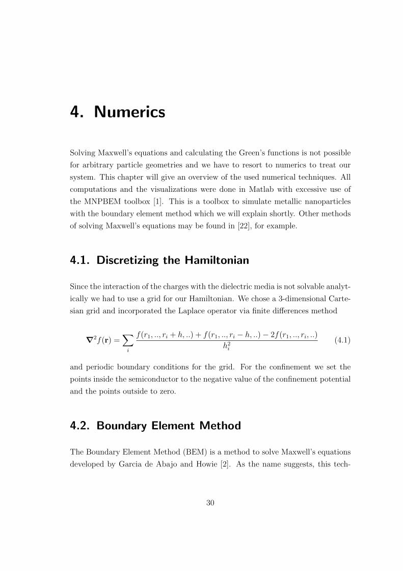
4.1. Discretizing the Hamiltonian
Since the interaction of the charges with the dielectric media is not solvable analyt-
ically we had to use a grid for our Hamiltonian. We chose a 3-dimensional Carte-
sian grid and incorporated the Laplace operator via finite differences method
∇2f(r) =∑i
f(r1, .., ri + h, ..) + f(r1, .., ri − h, ..)− 2f(r1, .., ri, ..)
h2i(4.1)
and periodic boundary conditions for the grid. For the confinement we set the
points inside the semiconductor to the negative value of the confinement potential
and the points outside to zero.
4.2. Boundary Element Method
The Boundary Element Method (BEM) is a method to solve Maxwell’s equations
developed by Garcia de Abajo and Howie [2]. As the name suggests, this tech-
30
4. Numerics
nique just discretizes the boundaries of a body rather than the whole volume of
the particle, as done in Discrete Dipole Approximation (DDA), lowering the re-
quirements for CPU time and memory. The catch is that it does not apply to
arbitrary dielectric environments but one has to make the following assumptions
for the involved media:
• homogeneous isotropic dielectric functions
• sharp boundaries between different media
But these assumptions are satisfied for most systems involving plasmonics, espe-
cially the systems covered in this thesis.
4.2.1. BEM theory
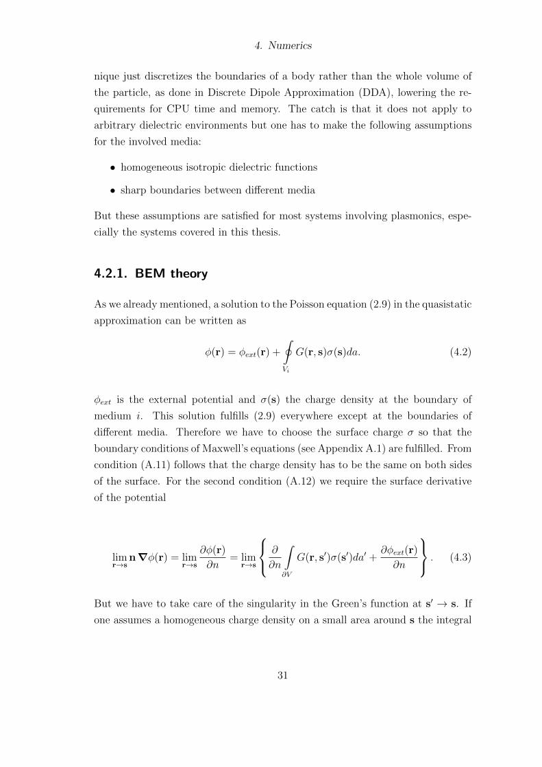
As we already mentioned, a solution to the Poisson equation (2.9) in the quasistatic
approximation can be written as
φ(r) = φext(r) +
∮Vi
G(r, s)σ(s)da. (4.2)
φext is the external potential and σ(s) the charge density at the boundary of
medium i. This solution fulfills (2.9) everywhere except at the boundaries of
different media. Therefore we have to choose the surface charge σ so that the
boundary conditions of Maxwell’s equations (see Appendix A.1) are fulfilled. From
condition (A.11) follows that the charge density has to be the same on both sides
of the surface. For the second condition (A.12) we require the surface derivative
of the potential
limr→s
n∇φ(r) = limr→s
∂φ(r)
∂n= lim
r→s
∂
∂n
∫∂V
G(r, s′)σ(s′)da′ +∂φext(r)
∂n
. (4.3)
But we have to take care of the singularity in the Green’s function at s′ → s. If
one assumes a homogeneous charge density on a small area around s the integral
31
4. Numerics
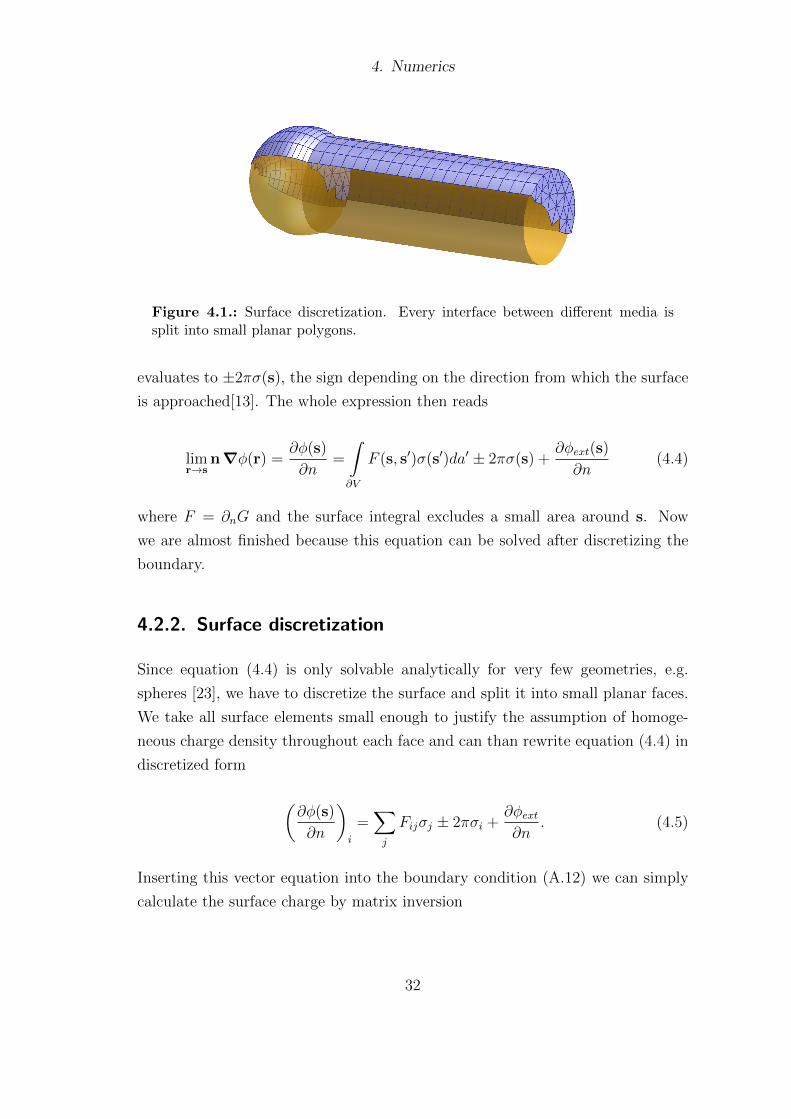
Figure 4.1.: Surface discretization. Every interface between different media issplit into small planar polygons.
evaluates to ±2πσ(s), the sign depending on the direction from which the surface
is approached[13]. The whole expression then reads
limr→s
n∇φ(r) =∂φ(s)
∂n=
∫∂V
F (s, s′)σ(s′)da′ ± 2πσ(s) +∂φext(s)
∂n(4.4)
where F = ∂nG and the surface integral excludes a small area around s. Now
we are almost finished because this equation can be solved after discretizing the
boundary.
4.2.2. Surface discretization
Since equation (4.4) is only solvable analytically for very few geometries, e.g.
spheres [23], we have to discretize the surface and split it into small planar faces.
We take all surface elements small enough to justify the assumption of homoge-
neous charge density throughout each face and can than rewrite equation (4.4) in
discretized form
(∂φ(s)
∂n
)i
=∑j
Fijσj ± 2πσi +∂φext∂n
. (4.5)
Inserting this vector equation into the boundary condition (A.12) we can simply
calculate the surface charge by matrix inversion
32
4. Numerics
σ = −(Λ− F)−1∂φext
∂n, (4.6)
with
Λ = 2πε2 + ε1ε2 − ε1
1
a matrix that incorporates the dielectric functions of the adjacent media.
With the knowledge of the surface charge we can compute the potentials, e.g. by
(2.2), and fields everywhere else. If we want to know the fields or potentials far
away, we simply put the charges in the middle of each face and treat them like
point charges. If we look closely to a particle surface we have to smear out the
charge over the face and integrate over the charge distribution to get accurate
results.
4.3. Program outline
This section outlines the structure of our approach. The approach can be divided
into three main parts:
• Initialization of particle:
Setting the geometry and discretization of the particle with MNPBEM tool-
box and defining material parameters
• Exciton wave functions:
We start with single particle wave functions of electron and hole calculated
by a simple particle-in-a-box approach. Then we calculate their self inter-
action and mutual interaction, which consists of a direct part and indirect
interaction through the environment. From this we then calculate the exci-
ton wave functions. More details can be found in section A.3.
• Optical response:
With the knowledge of the exciton wave functions we can calculate the co-
efficients for the polarization and therefore calculate the optical response as
33
4. Numerics
shown in section 3.3. Since the dielectric functions depend on light frequency
this calculations have to be looped over all incoming wavelengths.
Before we close this chapter we also want to mention the limiting factors of our
numerical approach. For the exciton self interaction we have to consider every
point of our space grid as an emitting and absorbing dipole and therefore we
have to calculate all the dyadic Green’s function for every combination of space
points. We also have to consider that many points are very close to the surface
and we can not use the approximation of point charges on the surfaces but have
to integrate over the homogeneous charge distribution on each surface element in
many cases. This two factors lead to a rapid increase of memory and time demands
dependent on the grid size. The computations for the optical response part, which
is the most time demanding task in this scheme, have to be done separately for
each excitation wavelength and the computation time increases linearly with the
energy resolution.
34
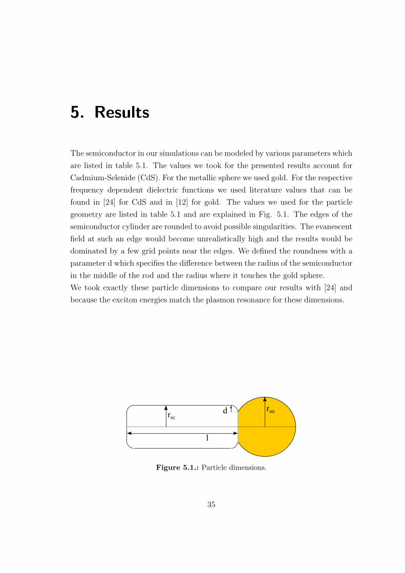
5. Results
The semiconductor in our simulations can be modeled by various parameters which
are listed in table 5.1. The values we took for the presented results account for
Cadmium-Selenide (CdS). For the metallic sphere we used gold. For the respective
frequency dependent dielectric functions we used literature values that can be
found in [24] for CdS and in [12] for gold. The values we used for the particle
geometry are listed in table 5.1 and are explained in Fig. 5.1. The edges of the
semiconductor cylinder are rounded to avoid possible singularities. The evanescent
field at such an edge would become unrealistically high and the results would be
dominated by a few grid points near the edges. We defined the roundness with a
parameter d which specifies the difference between the radius of the semiconductor
in the middle of the rod and the radius where it touches the gold sphere.
We took exactly these particle dimensions to compare our results with [24] and
because the exciton energies match the plasmon resonance for these dimensions.
rsc
raud
l
Figure 5.1.: Particle dimensions.
35
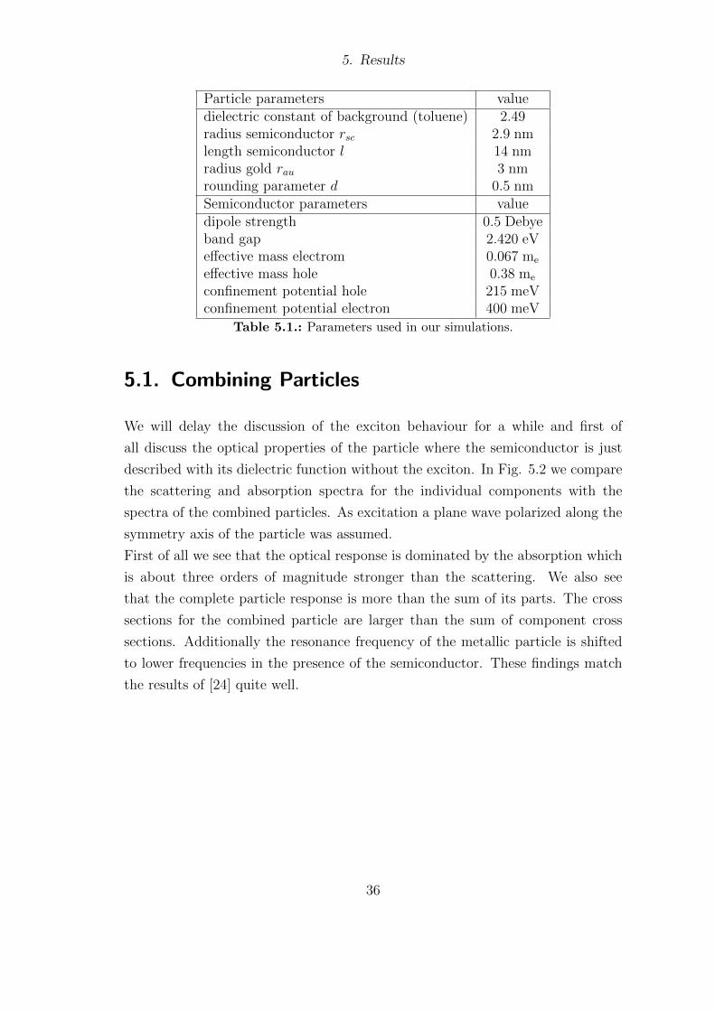
5. Results
Particle parameters valuedielectric constant of background (toluene) 2.49radius semiconductor rsc 2.9 nmlength semiconductor l 14 nmradius gold rau 3 nmrounding parameter d 0.5 nmSemiconductor parameters valuedipole strength 0.5 Debyeband gap 2.420 eVeffective mass electrom 0.067 me
effective mass hole 0.38 me
confinement potential hole 215 meVconfinement potential electron 400 meV
Table 5.1.: Parameters used in our simulations.
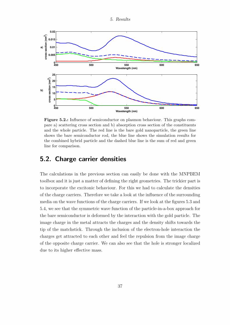
5.1. Combining Particles
We will delay the discussion of the exciton behaviour for a while and first of
all discuss the optical properties of the particle where the semiconductor is just
described with its dielectric function without the exciton. In Fig. 5.2 we compare
the scattering and absorption spectra for the individual components with the
spectra of the combined particles. As excitation a plane wave polarized along the
symmetry axis of the particle was assumed.
First of all we see that the optical response is dominated by the absorption which
is about three orders of magnitude stronger than the scattering. We also see
that the complete particle response is more than the sum of its parts. The cross
sections for the combined particle are larger than the sum of component cross
sections. Additionally the resonance frequency of the metallic particle is shifted
to lower frequencies in the presence of the semiconductor. These findings match
the results of [24] quite well.
36
5. Results
450 500 550 600 6500
0.005
0.01
0.015
0.02
Wavelength (nm)
cro
ss
se
cti
on
(n
m2)
a)
450 500 550 600 6500
5
10
15
20
25
Wavelength (nm)
cro
ss
se
cti
on
(n
m2)
b)
Figure 5.2.: Influence of semiconductor on plasmon behaviour. This graphs com-pare a) scattering cross section and b) absorption cross section of the constituentsand the whole particle. The red line is the bare gold nanoparticle, the green lineshows the bare semiconductor rod, the blue line shows the simulation results forthe combined hybrid particle and the dashed blue line is the sum of red and greenline for comparison.
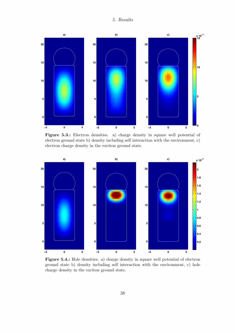
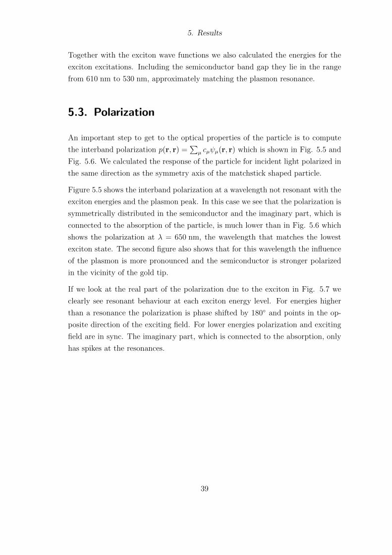
5.2. Charge carrier densities
The calculations in the previous section can easily be done with the MNPBEM
toolbox and it is just a matter of defining the right geometries. The trickier part is
to incorporate the excitonic behaviour. For this we had to calculate the densities
of the charge carriers. Therefore we take a look at the influence of the surrounding
media on the wave functions of the charge carriers. If we look at the figures 5.3 and
5.4, we see that the symmetric wave function of the particle-in-a-box approach for
the bare semiconductor is deformed by the interaction with the gold particle. The
image charge in the metal attracts the charges and the density shifts towards the
tip of the matchstick. Through the inclusion of the electron-hole interaction the
charges get attracted to each other and feel the repulsion from the image charge
of the opposite charge carrier. We can also see that the hole is stronger localized
due to its higher effective mass.
37
5. Results
−5 0 5
0
5
10
15
20
a)
−5 0 5
0
5
10
15
20
b)
−5 0 5
0
5
10
15
20
c)
0
5
10
15x 10
−3
Figure 5.3.: Electron densities. a) charge density in square well potential ofelectron ground state b) density including self interaction with the environment, c)electron charge density in the exciton ground state.
−5 0 5
0
5
10
15
20
a)
−5 0 5
0
5
10
15
20
b)
−5 0 5
0
5
10
15
20
c)
0.2
0.4
0.6
0.8
1
1.2
1.4
1.6
1.8
2
x 10−3
Figure 5.4.: Hole densities. a) charge density in square well potential of electronground state b) density including self interaction with the environment, c) holecharge density in the exciton ground state.
38
5. Results
Together with the exciton wave functions we also calculated the energies for the
exciton excitations. Including the semiconductor band gap they lie in the range
from 610 nm to 530 nm, approximately matching the plasmon resonance.
5.3. Polarization
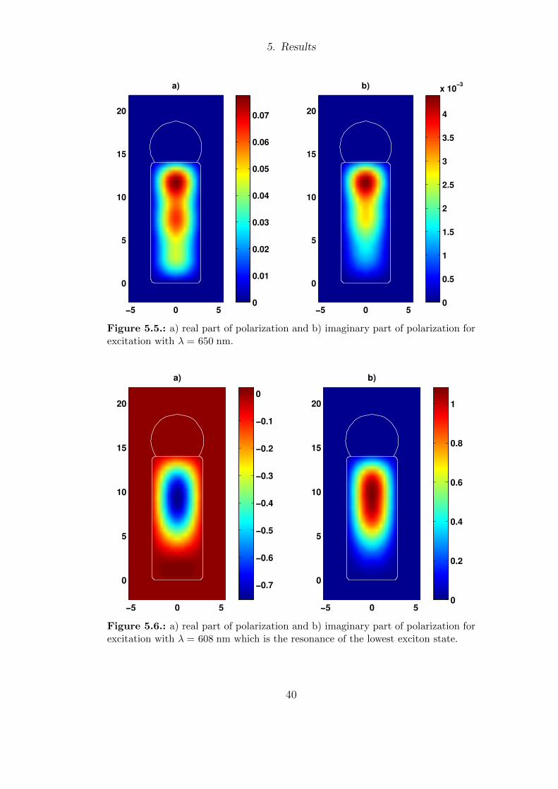
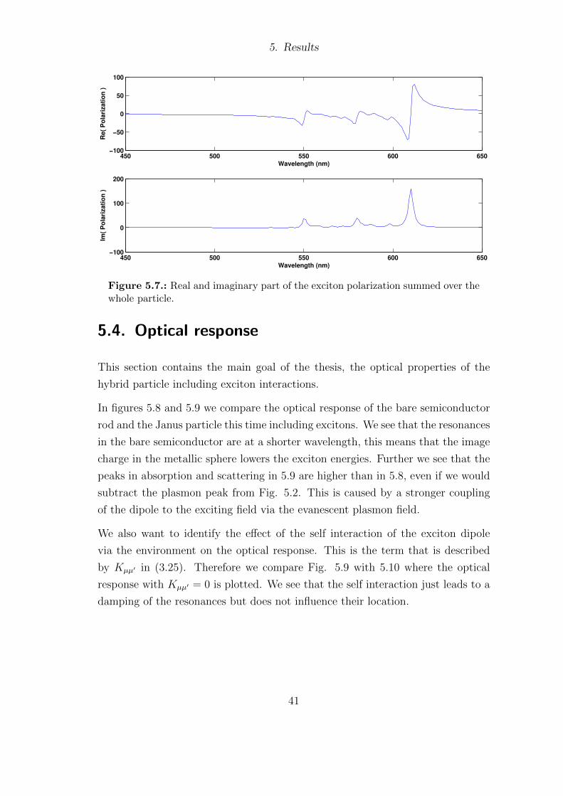
An important step to get to the optical properties of the particle is to compute
the interband polarization p(r, r) =∑
µ cµψµ(r, r) which is shown in Fig. 5.5 and
Fig. 5.6. We calculated the response of the particle for incident light polarized in
the same direction as the symmetry axis of the matchstick shaped particle.
Figure 5.5 shows the interband polarization at a wavelength not resonant with the
exciton energies and the plasmon peak. In this case we see that the polarization is
symmetrically distributed in the semiconductor and the imaginary part, which is
connected to the absorption of the particle, is much lower than in Fig. 5.6 which
shows the polarization at λ = 650 nm, the wavelength that matches the lowest
exciton state. The second figure also shows that for this wavelength the influence
of the plasmon is more pronounced and the semiconductor is stronger polarized
in the vicinity of the gold tip.
If we look at the real part of the polarization due to the exciton in Fig. 5.7 we
clearly see resonant behaviour at each exciton energy level. For energies higher
than a resonance the polarization is phase shifted by 180 and points in the op-
posite direction of the exciting field. For lower energies polarization and exciting
field are in sync. The imaginary part, which is connected to the absorption, only
has spikes at the resonances.
39
5. Results
−5 0 5
0
5
10
15
20
a)
0
0.01
0.02
0.03
0.04
0.05
0.06
0.07
−5 0 5
0
5
10
15
20
b)
0
0.5
1
1.5
2
2.5
3
3.5
4
x 10−3
Figure 5.5.: a) real part of polarization and b) imaginary part of polarization forexcitation with λ = 650 nm.
−5 0 5
0
5
10
15
20
a)
−0.7
−0.6
−0.5
−0.4
−0.3
−0.2
−0.1
0
−5 0 5
0
5
10
15
20
b)
0
0.2
0.4
0.6
0.8
1
Figure 5.6.: a) real part of polarization and b) imaginary part of polarization forexcitation with λ = 608 nm which is the resonance of the lowest exciton state.
40
5. Results
450 500 550 600 650−100
−50
0
50
100
Wavelength (nm)
Re
( P
ola
riza
tio
n )
450 500 550 600 650−100
0
100
200
Wavelength (nm)
Im(
Po
lari
za
tio
n )
Figure 5.7.: Real and imaginary part of the exciton polarization summed over thewhole particle.
5.4. Optical response
This section contains the main goal of the thesis, the optical properties of the
hybrid particle including exciton interactions.
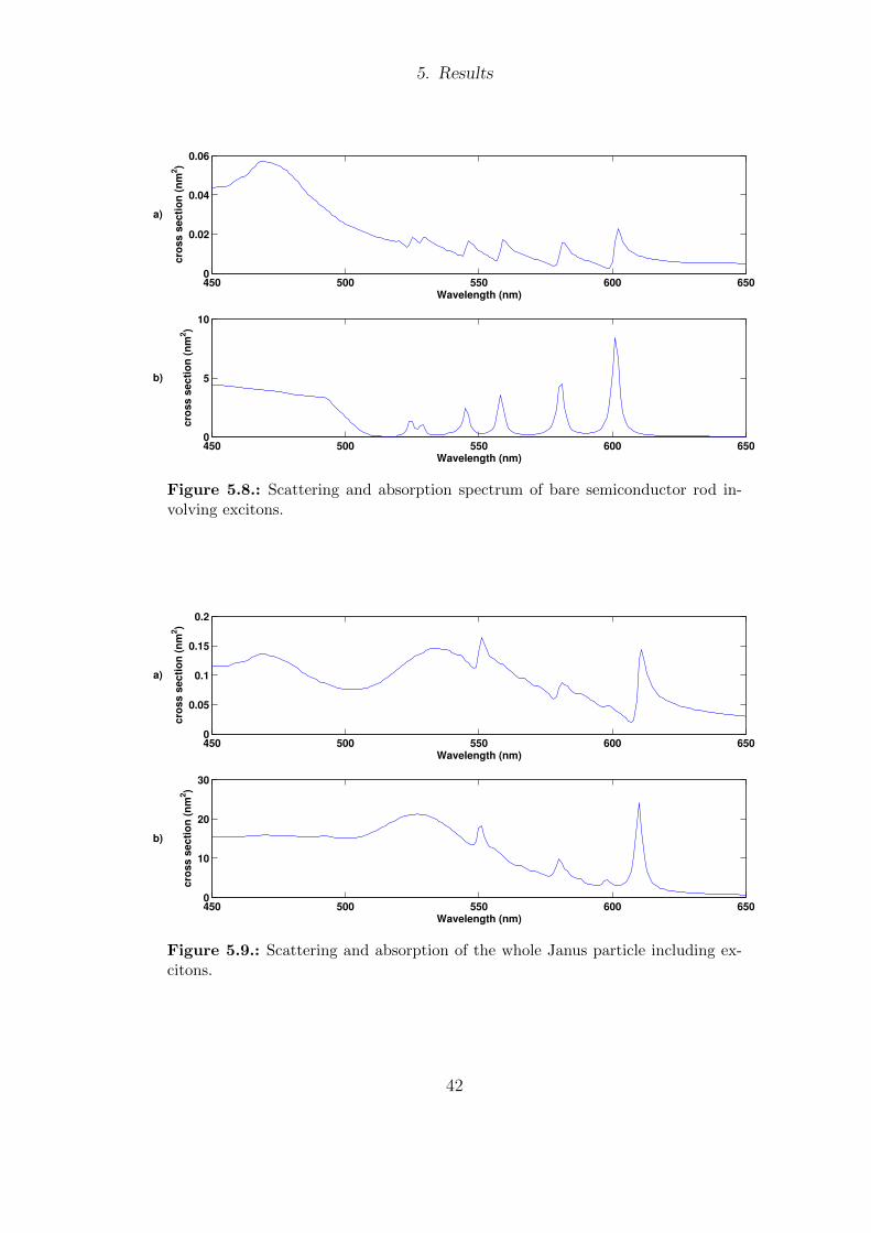
In figures 5.8 and 5.9 we compare the optical response of the bare semiconductor
rod and the Janus particle this time including excitons. We see that the resonances
in the bare semiconductor are at a shorter wavelength, this means that the image
charge in the metallic sphere lowers the exciton energies. Further we see that the
peaks in absorption and scattering in 5.9 are higher than in 5.8, even if we would
subtract the plasmon peak from Fig. 5.2. This is caused by a stronger coupling
of the dipole to the exciting field via the evanescent plasmon field.
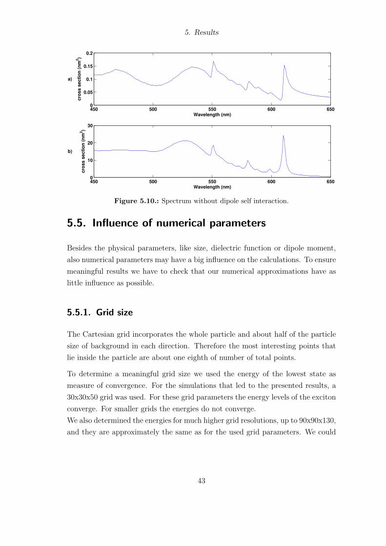
We also want to identify the effect of the self interaction of the exciton dipole
via the environment on the optical response. This is the term that is described
by Kµµ′ in (3.25). Therefore we compare Fig. 5.9 with 5.10 where the optical
response with Kµµ′ = 0 is plotted. We see that the self interaction just leads to a
damping of the resonances but does not influence their location.
41
5. Results
450 500 550 600 6500
0.02
0.04
0.06
Wavelength (nm)
cro
ss
se
cti
on
(n
m2)
a)
450 500 550 600 6500
5
10
Wavelength (nm)
cro
ss
se
cti
on
(n
m2)
b)
Figure 5.8.: Scattering and absorption spectrum of bare semiconductor rod in-volving excitons.
450 500 550 600 6500
0.05
0.1
0.15
0.2
Wavelength (nm)
cro
ss
se
cti
on
(n
m2)
a)
450 500 550 600 6500
10
20
30
Wavelength (nm)
cro
ss
se
cti
on
(n
m2)
b)
Figure 5.9.: Scattering and absorption of the whole Janus particle including ex-citons.
42
5. Results
450 500 550 600 6500
0.05
0.1
0.15
0.2
Wavelength (nm)
cro
ss
se
cti
on
(n
m2)
a)
450 500 550 600 6500
10
20
30
Wavelength (nm)
cro
ss
se
cti
on
(n
m2)
b)
Figure 5.10.: Spectrum without dipole self interaction.
5.5. Influence of numerical parameters
Besides the physical parameters, like size, dielectric function or dipole moment,
also numerical parameters may have a big influence on the calculations. To ensure
meaningful results we have to check that our numerical approximations have as
little influence as possible.
5.5.1. Grid size
The Cartesian grid incorporates the whole particle and about half of the particle
size of background in each direction. Therefore the most interesting points that
lie inside the particle are about one eighth of number of total points.
To determine a meaningful grid size we used the energy of the lowest state as
measure of convergence. For the simulations that led to the presented results, a
30x30x50 grid was used. For these grid parameters the energy levels of the exciton
converge. For smaller grids the energies do not converge.
We also determined the energies for much higher grid resolutions, up to 90x90x130,
and they are approximately the same as for the used grid parameters. We could
43
5. Results
not use this high resolution for the whole calculations because of memory and
time limitations.
5.5.2. Number of states
To calculate the exciton wave functions we used products of one particle wave
functions of electrons and holes, see equation (A.28). Therefore we needed a
numerical cut off for the number of these single particle wave functions. We took
all states below the confinement energy because we are only interested in the
charges that are confined to the semiconductor (bound states).
5.6. Problems
In the first calculations we used a particle without rounded edges. But sharp
edges led to unrealistically high fields. Together with the approximation that was
incorporated by the grid approach, grid points near these edges had an dispropor-
tionately high influence on the results.
5.7. Conclusion
In this thesis we studied optical properties of a semiconductor-metal hybrid
nanoparticle. We developed a scheme to describe the polarization due to the
excitons created in the semiconductor within the linear field regime. We used the
MNPBEM toolbox [1], that is based on the boundary element method, to derive
the Green’s functions for our system. With these Green’s functions we were able
to calculate the exciton wave functions and the polarization dynamics.
In a simple dielectric simulation, neglecting exciton effects, we saw that the scat-
tering and absorption cross section of the combined particle is larger than the sum
of the optical response of the different components.
44
5. Results
We saw that the exciton energies in the combined particle are lowered due to
image charges in the metallic particle. This also leads to a stronger localization
of the exciton near the metal-semiconductor interface.
As expected the optical response of the excitons mainly depends on the strength
of the interband dipole moment d. Typically it is in the range from 0.1 to 1 Debye.
In our calculations we assumed it to be 0.5 Debye. The strength of the exciton
resonances also depend on their relative location to the plasmon peak because
they are enhanced by the evanescent field of the plasmonic particle. The electron
self interaction with the environment, which is described by Kµµ′ , just has a little
damping effect but no effect on the resonance frequencies.
45
Acknowledgements
First of all I want to thank my mother and my grandparents for their great support.
You are the ones who made it possible for me to study in this interesting field.
I want to thank Univ. Prof. Ulrich Hohenester for the exceptional supervision.
He always had an open door for my questions, was inspiring with his intuition for
physics and made it fun to work in his group.
To my colleagues Andi, Toni, Rene and Benedikt i am grateful for their advice and
never letting it get too boring in the office. I also want to thank all the friends
and fellow students that helped me during the last years and made studying
physics interesting and fun. In that regard I especially want to thank Michi and
Sebastian with whom i had many entertaining and memorable experiences during
this time.
Finally I want to thank Johanna for her love and for kicking me in the butt when
I got too lazy.
46
A. Calculations
A.1. Boundary Conditions
To study the behaviour of the normal component of the electromagnetic field at
interfaces between dielectric media we look at equations (2.3a) and (2.3b) in their
integral form [4] ∮S
D · n da = 4π
∫ρdτ, (A.1)∮
S
B · n da = 0. (A.2)
We now take these integrals over the cylindric volume shown in Fig. A.1 but
place some restrictions on that volume. First of all we take the limit h → 0 for
the height of the cylinder and second we take a very thin cylinder, so we can
assume constant fields at the top and bottom area of the cylinder and a constant
charge density at the interface. In these limits we get for the left hand side of the
nΔa
h
Δl
ε1,μ1
E1,H1
Figure A.1.: Schematics for derivation of boundary conditions for Maxwell’s equa-tions
47
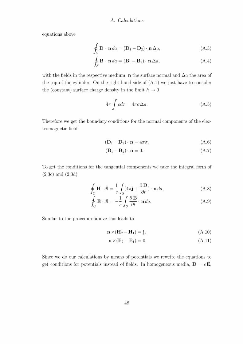
A. Calculations
equations above ∮S
D · n da = (D1−D2) · n ∆a, (A.3)∮S
B · n da = (B1−B2) · n ∆a, (A.4)
with the fields in the respective medium, n the surface normal and ∆a the area of
the top of the cylinder. On the right hand side of (A.1) we just have to consider
the (constant) surface charge density in the limit h→ 0
4π
∫ρdτ = 4πσ∆a. (A.5)
Therefore we get the boundary conditions for the normal components of the elec-
tromagnetic field
(D1−D2) · n = 4πσ, (A.6)
(B1−B2) · n = 0. (A.7)
To get the conditions for the tangential components we take the integral form of
(2.3c) and (2.3d) ∮C
H · dl =1
c
∫S
(4πj +∂D
∂t) · n da, (A.8)∮
C
E · dl = −1
c
∫S
∂B
∂t· n da. (A.9)
Similar to the procedure above this leads to
n×(H2−H1) = j, (A.10)
n×(E2−E1) = 0. (A.11)
Since we do our calculations by means of potentials we rewrite the equations to
get conditions for potentials instead of fields. In homogeneous media, D = εE,
48
A. Calculations
equation (A.6) can be rewritten as
ε1∂φ1
∂n− ε2
∂φ2
∂n= 4πσ (A.12)
where ∂/∂n is the derivative in the direction normal to the surface.
From the continuity of the tangential electric field (A.11) we get for the potential
(∇φ1)‖ = (∇φ2)
‖ (A.13)
A.2. Potentials in media
If we look at a system with free charges ρf and bound charges ρb we can introduce
two different potentials
∇2φ0 = −4πρf , (A.14)
∇2φ = −4π(ρf + ρb). (A.15)
These correspond to the electric displacement and the electric field
D = −∇φ0, (A.16)
E = −∇φ. (A.17)
In a homogeneous medium we can use the proportionality of of these fields, D =
εE, to introduce an additional differential operator
∇2φ0 = −∇D = −∇εE = ∇ε∇φ = −4πρf ,
∇ · ε∇ = ε∇2 + (∇ε) ·∇ = ε(∇2 + e).
49
A. Calculations
Therefore the new operator is defined as
e =1
ε(∇ε) ·∇. (A.18)
With the help of this operator we can deduce the free charge density directly from
the potential φ
(∇2 + e)φ = −4πρfε. (A.19)
The Green’s functions for the differential operators have to fulfill
∇2G0 = −4πδ(r− r′), (A.20)
(∇2 + e)G = −4πδ(r− r′), (A.21)
where G0 is the electrostatic Green’s function for unbound media that we already
encountered in section 2.1.3, G is a Green’s function that incorporates the geom-
etry of the system and in general has no simple analytic form. If we combine the
two equations above we can get
(∇2 + e)(G−G0) = eG0. (A.22)
Since G is the Green’s function to the occurring differential operator the solution
is
G−G0 =1
4πGeG0 =
1
4πG0eG, (A.23)
where the second equality is obtained by an iterative solution to this Dyson like
equation.
We can express φ through the Green’s function for (A.19) and get
∇2φ = −4πρfε− eφ = −4π
ρfε− eGρf
ε. (A.24)
50
A. Calculations
Inserting equation (A.14) on the left side gives
− 4π(ρf + ρb) = −4πρfε− eGρf
ε. (A.25)
We multiply this equation with G0 from the left and use (A.23) to get
G0ρb = G0(1
ε− 1)ρf + (G−G0)
ρfε
= (G
ε−G0)ρf . (A.26)
A.3. Exciton wave functions
To calculate the exciton wave functions, which we need for the calculation of
the optical response, we use products of the single particle wave functions φi of
electron and hole, i = e, h, which satisfy the Schrodinger equation
H0φiµ =
(−1
2∇2i + U i
conf
)φiµ = εiµφ
iµ. (A.27)
The exciton wave functions then are
ψ(re, rh) =∑µν
cµνψµν(re, rh) =∑µν
cµνφeµ(re)φ
hν(rh). (A.28)
Now we can set up the following Schrodinger equation
(−1
2∇2e −
1
2∇2h + U e
conf (re) + Uhconf (rh)−G(re, rh)
)ψ = Eψ, (A.29)
where G is the Greens function of the Coulomb interaction. It can be split into
three parts,
G(re, rh) = G0(re, rh) +Gind(re, rh) + Σ(re, rh). (A.30)
The direct interaction G0(r, r′) = 1/ε|r − r′|, the indirect Coulomb interaction
through induced charges Gind and Σ, the self interaction of the electron/hole via
51
A. Calculations
the environment. Here the latter two depend on the geometry of the system.
With the density matrix ρiµµ′ = φi†µφiµ′ , the representations of these operators in
our basis can be written as
〈µν|G0 |µ′ν ′〉 =
∫ρeµµ′(re)
1
ε|re − r′h|ρhνν′(rh)dτedτh
〈µν|Gind |µ′ν ′〉 =
∫ρeµµ′(re)G
ind(re, rh)ρhνν′(rh)dτdτ
′
〈µν|Σ |µ′ν ′〉 =1
2
∫φe
µ(re)Gind(re, re)φ
eµ(re)dτe · δνν′
+ δµµ′ ·1
2
∫φh
µ(rh)Gind(rh, rh)φ
hµ(rh)dτh,
where the one-half factor in the last equation follows from the adiabatic building
of the charge distribution [7].
Now we have all ingredients to construct the Hamiltonian in the single particle
basis. By diagonalizing it, we get the energy states and coefficients in (A.28) for
the excitonic wave functions of the complete system.
52
B. Conventions and Conversions
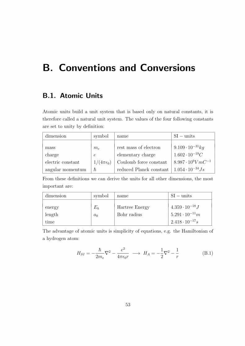
B.1. Atomic Units
Atomic units build a unit system that is based only on natural constants, it is
therefore called a natural unit system. The values of the four following constants
are set to unity by definition:
dimension symbol name SI− units
mass me rest mass of electron 9.109 · 10−31kg
charge e elementary charge 1.602 · 10−19C
electric constant 1/(4πε0) Coulomb force constant 8.987 · 109V mC−1
angular momentum h reduced Planck constant 1.054 · 10−34Js
From these definitions we can derive the units for all other dimensions, the most
important are:
dimension symbol name SI− units
energy Eh Hartree Energy 4.359 · 10−18J
length a0 Bohr radius 5.291 · 10−11m
time 2.418 · 10−17s
The advantage of atomic units is simplicity of equations, e.g. the Hamiltonian of
a hydrogen atom:
HSI = − h
2me
∇2 − e2
4πε0r−→ HA = −1
2∇2 − 1
r(B.1)
53
B. Conventions and Conversions
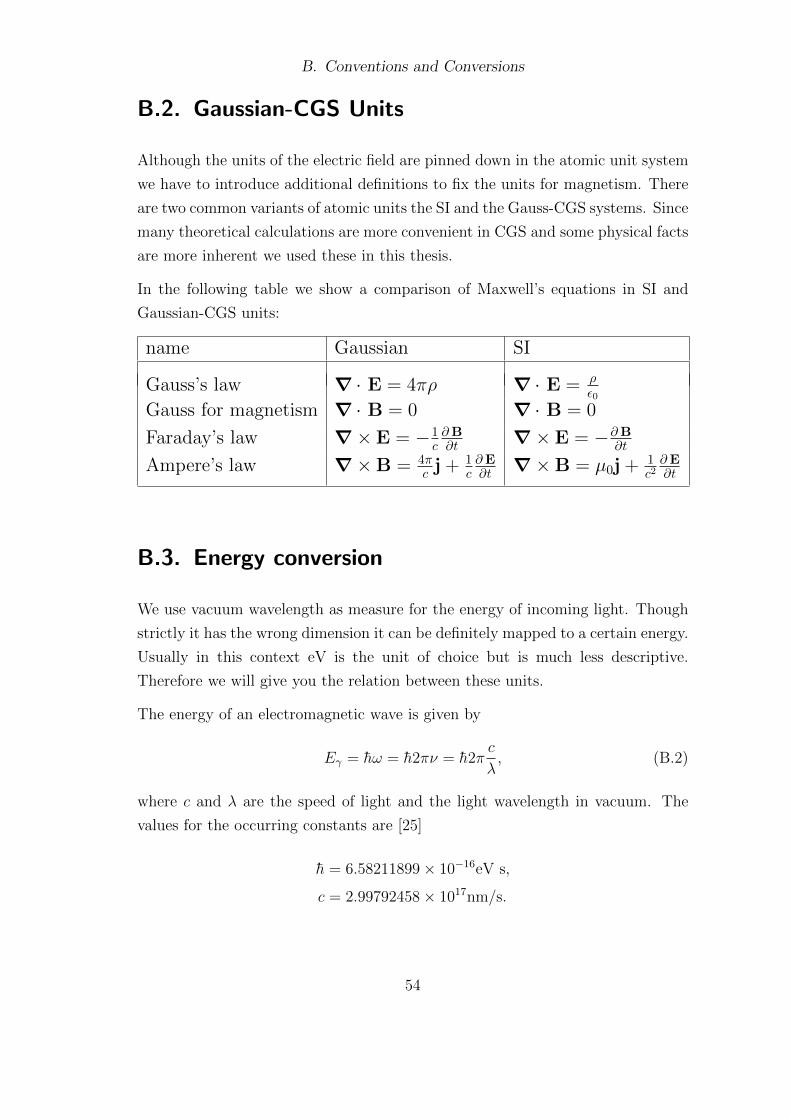
B.2. Gaussian-CGS Units
Although the units of the electric field are pinned down in the atomic unit system
we have to introduce additional definitions to fix the units for magnetism. There
are two common variants of atomic units the SI and the Gauss-CGS systems. Since
many theoretical calculations are more convenient in CGS and some physical facts
are more inherent we used these in this thesis.
In the following table we show a comparison of Maxwell’s equations in SI and
Gaussian-CGS units:
name Gaussian SI
Gauss’s law ∇ · E = 4πρ ∇ · E = ρε0
Gauss for magnetism ∇ · B = 0 ∇ · B = 0
Faraday’s law ∇× E = −1c∂B∂t ∇× E = −∂B
∂t
Ampere’s law ∇×B = 4πc j + 1
c∂E∂t ∇×B = µ0j + 1
c2∂E∂t
B.3. Energy conversion
We use vacuum wavelength as measure for the energy of incoming light. Though
strictly it has the wrong dimension it can be definitely mapped to a certain energy.
Usually in this context eV is the unit of choice but is much less descriptive.
Therefore we will give you the relation between these units.
The energy of an electromagnetic wave is given by
Eγ = hω = h2πν = h2πc
λ, (B.2)
where c and λ are the speed of light and the light wavelength in vacuum. The
values for the occurring constants are [25]
h = 6.58211899× 10⁻¹⁶eV s,
c = 2.99792458× 10¹⁷nm/s.
54

B. Conventions and Conversions
The conversion from vacuum wavelength to eV is therefore
E[eV] =1239.84
λ[nm]. (B.3)
Since we used Hartree units for many of our calculations we will additionally note
the relation between eV and Eh
E[Eh] = 27.211385 ·E[eV].
55
Bibliography
[1] Ulrich Hohenester and Andreas Trugler. Mnpbem - a matlab toolbox for the
simulation of plasmonic nanoparticles. Computer Physics Communications,
183(2):370–381, 2012.
[2] F. J. Garcıa de Abajo and A. Howie. Retarded field calculation of electron
energy loss in inhomogeneous dielectrics. Phys. Rev. B, 65:115418, Mar 2002.
[3] Harry A. Atwater. The promise of plasmonics. SIGDA Newsl., 37(9):1:1–1:1,
May 2007.
[4] John David Jackson. Classical Electrodynamics. Wiley, 1998.
[5] D.J. Griffiths. Introduction to electrodynamics. Prentice Hall, 1999.
[6] Charles Coulomb. Premier memoire sur l’electricite et le magnetisme. Histoire
de l’Academie royale des sciences, pages 569–577, 1785.
[7] L. Hedin and S. Lundqvist. Effects of electron-electron and electron-phonon
interactions on the one-electron states of solids. Solid State Physics, 23:1–181,
1969.
[8] James Clerk Maxwell. A dynamical theory of the electromagnetic field. Philo-
sophical Transactions of the Royal Society of London, 155:459–513, 1865.
[9] Ulrich Hohenester and Joachim Krenn. Surface plasmon resonances of single
and coupled metallic nanoparticles: A boundary integral method approach.
Phys. Rev. B, 72:195429, Nov 2005.
[10] L. Novotny and B. Hecht. Principles of Nano-Optics. Cambridge University
Press, 2006.
[11] S.A. Maier. Plasmonics: Fundamentals and Applications. Springer, 2007.
56
Bibliography
[12] E.D. Palik. Handbook of Optical Constants of Solids Five-volume Set: Hand-
book of optical constants of solids I, II, & III. Handbook of Optical Constants
of Solids Five-volume Set. Academic Press, 1998.
[13] Andreas Trugler. Optical properties of metallic nanoparticles. PhD thesis,
Karl-Franzens Universitat Graz, July 2011.
[14] E. Kretschmann and H. Raether. Radiative decay of nonradiative surface
plasmons excited by light. Z. Naturforsch. A, 23:2135, 1968.
[15] Andreas Otto. Excitation of nonradiative surface plasma waves in silver by
the method of frustrated total reflection. Zeitschrift fur Physik, 216:398–410,
1968.
[16] H. Haug and S.W. Koch. Quantum Theory of the Optical and Electronic
Properties of Semiconductors. World Scientific, 2004.
[17] K. Hess. Advanced theory of semiconductor devices. IEEE Press, 2000.
[18] Marlan O. Scully and M. Suhail Zubairy. Quantum Optics. Cambridge Uni-
versity Press, 2001.
[19] H.C. Van De Hulst. Light scattering: by small particles. Structure of Matter
Series. Dover Publications, 1957.
[20] V. M. Axt and S. Mukamel. Nonlinear optics of semiconductor and molecular
nanostructures; a common perspective. Rev. Mod. Phys., 70:145–174, Jan
1998.
[21] L.H. Ryder. Quantum Field Theory. Cambridge University Press, 1996.
[22] Viktor Myroshnychenko, Jessica Rodriguez-Fernandez, Isabel Pastoriza-
Santos, Alison M. Funston, Carolina Novo, Paul Mulvaney, Luis M. Liz-
Marzan, and F. Javier Garcia de Abajo. Modelling the optical response of
gold nanoparticles. Chem. Soc. Rev., 37:1792–1805, 2008.
[23] Gustav Mie. Beitrage zur optik truber medien, speziell kolloidaler metallosun-
gen. Annalen der Physik, 330(3):377–445, 1908.
57
Bibliography
[24] Ehud Shaviv, Olaf Schubert, Marcelo Alves-Santos, Guido Goldoni, Rosa
Di Felice, Fabrice Vallee, Natalia Del Fatti, Uri Banin, and Carsten Sonnich-
sen. Absorption properties of metal-semiconductor hybrid nanoparticles. ACS
Nano, 5(6):4712–4719, 2011.
[25] Peter J. Mohr, Barry N. Taylor, and David B. Newell. Codata recommended
values of the fundamential physical constanst: 2006. Rev. Mod. Phys., 80:633,
2008.
58