Optical Near Field Study of Ag Nanowires by the Differential...
8
Journal of Modern Physics, 2012, 3, 102-109 http://dx.doi.org/10.4236/jmp.2012.31014 Published Online January 2012 (http://www.SciRP.org/journal/jmp) Optical Near-Field Study of Ag Nanowires by the Differential Method Mohamed Zoheir Chekroun 1,2* , Ghaouti Bassou 1 , Laurent Salomon 2 , Aziz Zenati 3 , Ahmed Taalbi 1 , Hanifi Bendaoud 4 , Mohammed Ameri 3 1 Laboratoire de Microscopie, Microanalyse de la Matière et Spectroscopie Moléculaire, Université Djillali Liabes, Sidi Bel Abbes, Algérie 2 Groupe d’Optique de Champ Proche, Institut Carnot de Bourgogne (ICB), UMR CNRS, Université de Bourgogne, Dijon, France 3 Département de Physique, Faculté des Sciences, Université Djillali Liabes, Sidi Bel Abbes, Algérie 4 Laboratoire des Matériaux Appliqués, Université Djillali Liabes, Sidi Bel Abbes, Algérie Email: * [email protected] Received September 13, 2011; revised October 22, 2011; accepted November 10, 2011 ABSTRACT The optical response of subwavelength silver nanowires arranged periodically on silica has been analyzed numerically by the differential method improved by the S matrix algorithm. Our results improve the capacity of this rigorous method to give a description of various phenomena occurring in near and far-field around the periodic grating. This renders pos- sible to determine the positions of plasmon’s resonance according to the choice of materials used and the geometrical properties. We study the behavior of the diffracted light by the nano-structure in both single nanowire case and grating nanowires case. The influence of the exact grating period and the induced modification of the spacer nanowire depend- ence are then discussed. Moreover, we present mappings of the electromagnetic field located at 50 nm above the nanowires. Keywords: Near-Field; Differential Method; Nanowires; Plasmons; Silver 1. Introduction In recent years, surface plasmons (SPs) have gained at- tention because of their potential applications in nano- photonic and plasmonic devices [1-7]. Surface plasmons are electron charge density waves confined to and trav- eling along the surface between a metal and a dielectric. These electronic excitations are a consequence of the col- lective oscillation of the conduction band electrons in the metal [8]. They manifest themselves in strong field en- hancement near the metal surface. In the same way, va- rious photonic crystal structures with nanostructured me- tals have been realized so far. In addition to periodically modulated metal surfaces, including surface corrugation [9,10], regular arrangements of individual metal nanopar- ticles on dielectric substrates [11] are prominent examples of such polaritonic crystal structures. The particular opti- cal properties of metallic nanostructures can be attributed to the excitation surface plasmons [12]. The properties of the local enhanced field for a single isolated particle depend on the particle parameters, the properties of the incident irradiation and the surrounding medium [13-15]. As for nanoparticles array they can be additionally mo- dified by the interparticles coupling effect [16-18]. Surface enhanced effects, like surface enhanced Raman scattering or surface enhanced fluorescence [13,19-21] take advantage of both, the near-field and the far-field of resonantly excited metal nanoparticles: on one hand, the enhanced near-fields lead to a higher excitation efficiency and on the other hand, the nanoparticles act as a trans- mitting antenna and enhance the coupling of atomic or molecular resonances to the optical far-field. For the first one, the induced near electromagnetic field has properties of an evanescent wave, its amplitude decreases rapidly with the distance from the metal surface. Thus, the size of the field enhanced area is governed only by the size of the optically illuminated metal structure and the diffrac- tion limit can be overcome. The waveguiding of surface palsmon polaritons (SPPs) along one-dimensional structures has been attracting in- tensive attention. A number of ideas, such as planar metal waveguides [22], metallic nanohole grating [23], dielec- tric-loaded SPP waveguides [24] and metal nanowires [25] have been suggested for this aim. For all these structures, silver nanowires that can be routinely fabricated with smooth * Corresponding author. Copyright © 2012 SciRes. JMP
Transcript of Optical Near Field Study of Ag Nanowires by the Differential...
Journal of Modern Physics, 2012, 3, 102-109 http://dx.doi.org/10.4236/jmp.2012.31014 Published Online January 2012 (http://www.SciRP.org/journal/jmp)
Optical Near-Field Study of Ag Nanowires by the Differential Method
Mohamed Zoheir Chekroun1,2*, Ghaouti Bassou1, Laurent Salomon2, Aziz Zenati3, Ahmed Taalbi1, Hanifi Bendaoud4, Mohammed Ameri3
1Laboratoire de Microscopie, Microanalyse de la Matière et Spectroscopie Moléculaire, Université Djillali Liabes, Sidi Bel Abbes, Algérie
2Groupe d’Optique de Champ Proche, Institut Carnot de Bourgogne (ICB), UMR CNRS, Université de Bourgogne, Dijon, France
3Département de Physique, Faculté des Sciences, Université Djillali Liabes, Sidi Bel Abbes, Algérie 4Laboratoire des Matériaux Appliqués, Université Djillali Liabes, Sidi Bel Abbes, Algérie
Email: *[email protected]
Received September 13, 2011; revised October 22, 2011; accepted November 10, 2011
ABSTRACT
The optical response of subwavelength silver nanowires arranged periodically on silica has been analyzed numerically by the differential method improved by the S matrix algorithm. Our results improve the capacity of this rigorous method to give a description of various phenomena occurring in near and far-field around the periodic grating. This renders pos- sible to determine the positions of plasmon’s resonance according to the choice of materials used and the geometrical properties. We study the behavior of the diffracted light by the nano-structure in both single nanowire case and grating nanowires case. The influence of the exact grating period and the induced modification of the spacer nanowire depend- ence are then discussed. Moreover, we present mappings of the electromagnetic field located at 50 nm above the nanowires. Keywords: Near-Field; Differential Method; Nanowires; Plasmons; Silver
1. Introduction
In recent years, surface plasmons (SPs) have gained at- tention because of their potential applications in nano- photonic and plasmonic devices [1-7]. Surface plasmons are electron charge density waves confined to and trav- eling along the surface between a metal and a dielectric. These electronic excitations are a consequence of the col- lective oscillation of the conduction band electrons in the metal [8]. They manifest themselves in strong field en- hancement near the metal surface. In the same way, va- rious photonic crystal structures with nanostructured me- tals have been realized so far. In addition to periodically modulated metal surfaces, including surface corrugation [9,10], regular arrangements of individual metal nanopar- ticles on dielectric substrates [11] are prominent examples of such polaritonic crystal structures. The particular opti- cal properties of metallic nanostructures can be attributed to the excitation surface plasmons [12].
The properties of the local enhanced field for a single isolated particle depend on the particle parameters, the properties of the incident irradiation and the surrounding
medium [13-15]. As for nanoparticles array they can be additionally mo-
dified by the interparticles coupling effect [16-18]. Surface enhanced effects, like surface enhanced Raman
scattering or surface enhanced fluorescence [13,19-21] take advantage of both, the near-field and the far-field of resonantly excited metal nanoparticles: on one hand, the enhanced near-fields lead to a higher excitation efficiency and on the other hand, the nanoparticles act as a trans-mitting antenna and enhance the coupling of atomic or molecular resonances to the optical far-field. For the first one, the induced near electromagnetic field has properties of an evanescent wave, its amplitude decreases rapidly with the distance from the metal surface. Thus, the size of the field enhanced area is governed only by the size of the optically illuminated metal structure and the diffrac-tion limit can be overcome.
The waveguiding of surface palsmon polaritons (SPPs) along one-dimensional structures has been attracting in- tensive attention. A number of ideas, such as planar metal waveguides [22], metallic nanohole grating [23], dielec- tric-loaded SPP waveguides [24] and metal nanowires [25] have been suggested for this aim. For all these structures, silver nanowires that can be routinely fabricated with smooth *Corresponding author.
Copyright © 2012 SciRes. JMP

M. Z. CHEKROUN ET AL. 103
surfaces and uniform diameters are one of the most con- sidered systems [25,26].
We have compared experimental results obtained by Schider et al. [27], with our simulations performed by the Differential Method [28-34] improved by S-algorithm [35,36], Li remarks [37] and the Redheffers star product [38] when the number of matrix multiplications can be further reduced remarquably. The versatility of the differential me- thod is demonstrated by considering complex configura-tions. In this respect, this method can be an easy-to-imple- ment alternative to more conventional method such as FDTD or finite elements. The nanowire gratings strongly depend on the polarization direction of the incident light. The excitation of dipolar plasmon mode is predominant when the polarization direction is perpendicular to the wire axis.
The paper is organized as follows. In Section 2, the numerical method we use to model the optical and plas- monic properties of the gratings is introduced. The re- sults of our calculations of the extinction properties of the nanostructures are presented and discussed in Section 3 distinguishing the noninteracting particles case from the grating configuration both in far and near-field. Finally, the conclusion is drawn in Section 4.
2. Numerical Method
To our knowledge, scalar electromagnetic theory, which has been widely used to compute the characteristics of dif- fractive gratings, is valid only for structures that are large compared to the incident wavelength, and the diffracted field can not be computed near the surface vicinity. For near-field, on sub-wavelength features, it is necessary to solve the full vector form of Maxwell’s equations under suitable boundary conditions [39,40]. There are some re- ported numerical calculation methods based on rigorous electromagnetic theory, such as time-domain finite diffe- rence method [41-44], boundary element, finite element method, Fourier modal method, etc.
Among these methods, the differential method [28-31] is one of the macroscopic methods allowing the calcula- tion of the intensity of light diffracted by an object. It is also based on Maxwell equations and the different boun- dary conditions at interfaces. The principle of this tech- nique consists of establishing the propagation equations of the electromagnetic field in different regions of space and calculating its components amplitudes.
This method has been performed with an S-algorithm; taking into account Li remarks [35-37] which is aimed for achieving unconditional numerical stability with S-al- gorithms is to avoid the exponentially growing functions in every step of the matrix recursion, and assuming a pe- riodic arrangement of metal wires. This algorithm is used to reduce the numerical instabilities linked with the exis- tence of increasing exponential functions during the nu-
merical integration process, that is exponential functions linked with evanescent orders, the electric and magnetic fields above the surface are presented as an expansion over Rayleigh waves. To find their complex amplitudes, the propagation equations are to be solved with boundary conditions at the two surfaces of the metal film. When the amplitude are calculated, the transmitted intensity as well as the electric and magnetic field distributions can be ob- tained by summation over all the modes. A finite number of modes in the calculations was chosen according to the stability of the numerical procedure. The numerical result was checked by calculation of the energy conservation and the convergence of the extinction while increasing the num- ber of modes.
We have studied a one dimensional structure (Figure 1) consisting of silver film of thickness h with a periodi- cal set of rectangular wires (D is a grating period, w is the wire width and h is the wire height). The structure is deposited on a substrate of glass (n = 1.458).
In all calculations below, the structure is illuminated in normal incidence with P-polarized light. In order to ob- tain good results, we injected into the simulation program a great number of modes (i.e. numbers of vectors) to cor- rect the numerical errors.
The input parameters of the method are the geometri- cal sizes of the structure and the dielectric susceptibilities of the constituent materials. The latter are treated as spa- tially local and frequency dependent, which is especially important in the case of metals. The dielectric function of silver was taken from Ref. [45].
3. Results and Discussion
3.1. Noninteracting Nanowires
3.1.1. Far-Field Case Silver is a paradigmatic case for studying surface plas- mons and there are a large amount of literatures on sur- face polariton plasmons (SPPs) by gratings [12,46-49] in the visible region. The reason for that is because at these wavelengths the imaginary part of the permittivity ( ) is small, then the SPs is well defined [12,50].
2E
Figure 1. Schematic of a nanostructured film with the nota-tions used for the numerical work.
Copyright © 2012 SciRes. JMP
M. Z. CHEKROUN ET AL. 104
We measure the optical extinction which is defined as 0 . log T TExt , where 0T and T denote the optical
transmission through the bare substrate and the nanowire sample deposited on the substrate, respectively.
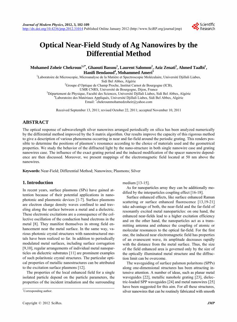
For instance, Schider et al. found, by fabricating one- dimensional silver nanowires (D = 2250 nm) with a cross section of 83 nm in width (w) and 25 nm in height (h) on a quartz substrate, that the optical response of regularly patterned nanowires strongly depends on the polarization of the incident light [27]. The extinction spectra produced by differential method (Figure 2(b)), are in excellent agree- ment with experimentally obtained results [27] shown in (Figure 2(a)); for our simulated results, the extinction
(a)
(b)
Figure 2. Extinction spectra of silver nanowires with pa-rameters w = 83 nm, h = 25 nm and D = 2250 nm under P polarization incident light are shown. (a) Experimental curve from reference [27] and (b) from our simulated work.
maximum is located near 490 nm and the full width at half maximum (FWHM) is approximately 180 nm. In the same case, experimental results show that the SPs reso- nance wavelength is near 495 nm and the FWHM is near 140 nm.
The extinction slightly grows with increased wavelengths due to the absorption of silver. Note that the position of an extinction peak indicates the resonance wavelength while the spectral width exhibits the damping of plasmon reso- nance induced by nanowires.
Starting from these two figures (Figures 2(a)-(b)), we notice a light shift between the experimental and numeri-cal wavelength of resonance, this can be explained by the conditions of manufacture of the samples (defects, aspe- rities) and experimental measurement.
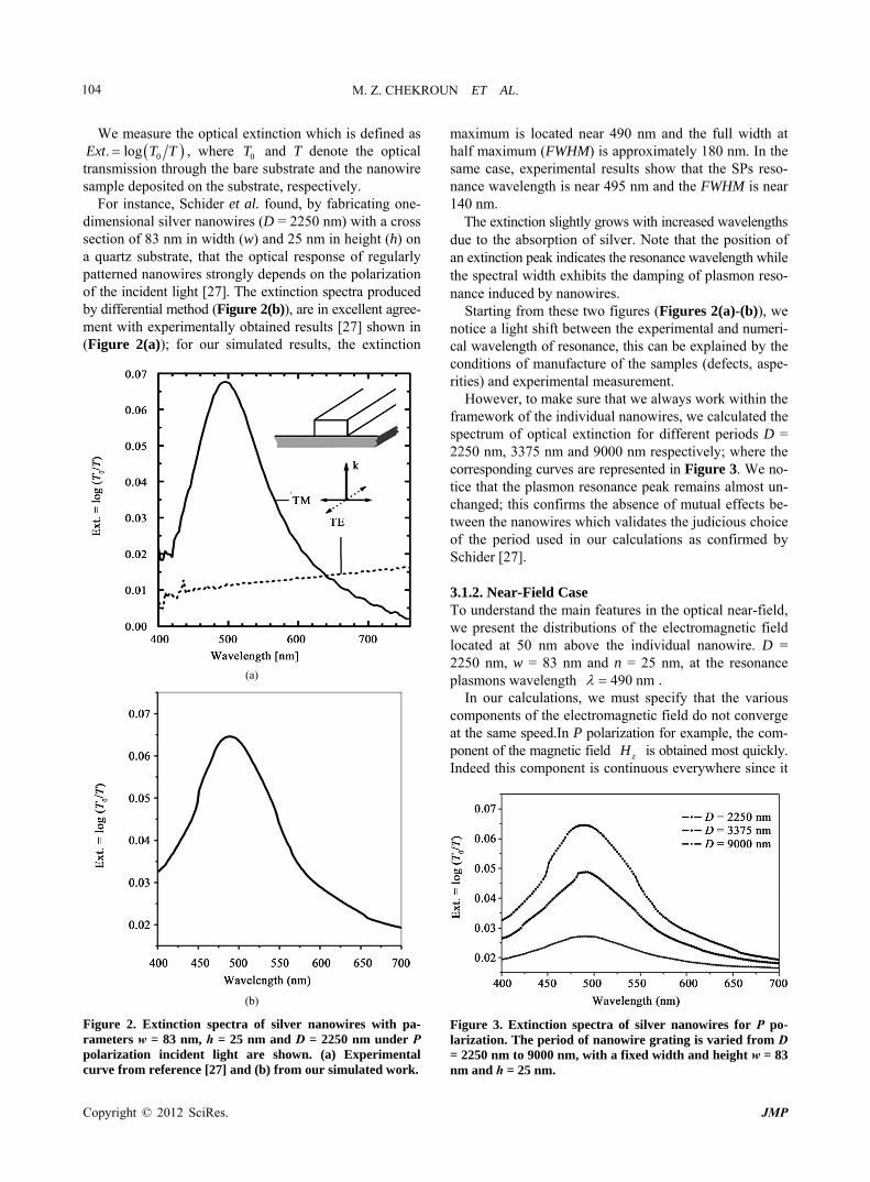
However, to make sure that we always work within the framework of the individual nanowires, we calculated the spectrum of optical extinction for different periods D = 2250 nm, 3375 nm and 9000 nm respectively; where the corresponding curves are represented in Figure 3. We no- tice that the plasmon resonance peak remains almost un- changed; this confirms the absence of mutual effects be- tween the nanowires which validates the judicious choice of the period used in our calculations as confirmed by Schider [27].
3.1.2. Near-Field Case To understand the main features in the optical near-field, we present the distributions of the electromagnetic field located at 50 nm above the individual nanowire. D = 2250 nm, w = 83 nm and n = 25 nm, at the resonance plasmons wavelength 490 nm .
In our calculations, we must specify that the various components of the electromagnetic field do not converge at the same speed.In P polarization for example, the com- ponent of the magnetic field zH is obtained most quickly. Indeed this component is continuous everywhere since it
Figure 3. Extinction spectra of silver nanowires for P po-larization. The period of nanowire grating is varied from D = 2250 nm to 9000 nm, with a fixed width and height w = 83 nm and h = 25 nm.
Copyright © 2012 SciRes. JMP
M. Z. CHEKROUN ET AL. 105
is necessarily parallel to each interface. As for the com- ponents of the electric field x 0
d msp
d m
E Ek k
E
E and yE , they have strong amplitudes at the metal interfaces. This leads to instabili- ties that are more significant, and in order to obtain the electromagnetic field map, we need to use a significant number of modes.
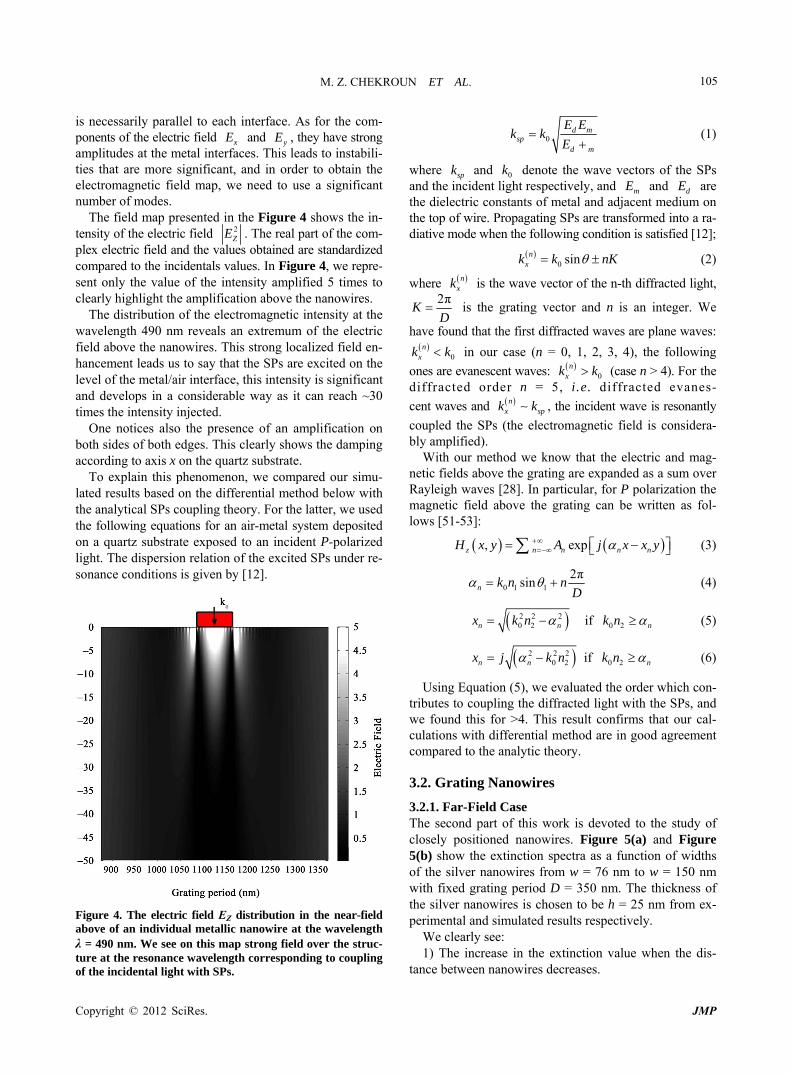
The field map presented in the Figure 4 shows the in-tensity of the electric field 2
ZE . The real part of the com- plex electric field and the values obtained are standardized compared to the incidentals values. In Figure 4, we repre- sent only the value of the intensity amplified 5 times to clearly highlight the amplification above the nanowires.
The distribution of the electromagnetic intensity at the wavelength 490 nm reveals an extremum of the electric field above the nanowires. This strong localized field en- hancement leads us to say that the SPs are excited on the level of the metal/air interface, this intensity is significant and develops in a considerable way as it can reach ~30 times the intensity injected.
One notices also the presence of an amplification on both sides of both edges. This clearly shows the damping according to axis x on the quartz substrate.
To explain this phenomenon, we compared our simu- lated results based on the differential method below with the analytical SPs coupling theory. For the latter, we used the following equations for an air-metal system deposited on a quartz substrate exposed to an incident P-polarized light. The dispersion relation of the excited SPs under re- sonance conditions is given by [12].
Figure 4. The electric field EZ distribution in the near-field above of an individual metallic nanowire at the wavelength λ = 490 nm. We see on this map strong field over the struc-ture at the resonance wavelength corresponding to coupling of the incidental light with SPs.
(1)
where sp and 0 denote the wave vectors of the SPs and the incident light respectively, and m and d are the dielectric constants of metal and adjacent medium on the top of wire. Propagating SPs are transformed into a ra- diative mode when the following condition is satisfied [12];
k kE E
0 sinn
xk k nK n
(2)
where xk is the wave vector of the n-th diffracted light, 2π
KD
0
nxk k
is the grating vector and n is an integer. We
have found that the first diffracted waves are plane waves:
in our case (n = 0, 1, 2, 3, 4), the following ones are evanescent waves: 0x (case n > 4). For the diffracted order n = 5, i.e. diffracted evanes-
nk k
ncent waves and x spk k , the incident wave is resonantly
coupled the SPs (the electromagnetic field is considera- bly amplified).
With our method we know that the electric and mag- netic fields above the grating are expanded as a sum over Rayleigh waves [28]. In particular, for P polarization the magnetic field above the grating can be written as fol- lows [51-53]:
, expz n n n nx y A j x x y H (3)
0 1 1
2πsinn k n n
D
(4)
2 2 20 2 0 2if n n nx k n k n
(5)
2 2 20 2 0 2if n n nx j k n k n (6)
Using Equation (5), we evaluated the order which con- tributes to coupling the diffracted light with the SPs, and we found this for >4. This result confirms that our cal- culations with differential method are in good agreement compared to the analytic theory.
3.2. Grating Nanowires
3.2.1. Far-Field Case The second part of this work is devoted to the study of closely positioned nanowires. Figure 5(a) and Figure 5(b) show the extinction spectra as a function of widths of the silver nanowires from w = 76 nm to w = 150 nm with fixed grating period D = 350 nm. The thickness of the silver nanowires is chosen to be h = 25 nm from ex- perimental and simulated results respectively.
We clearly see: 1) The increase in the extinction value when the dis-
tance between nanowires decreases.
Copyright © 2012 SciRes. JMP

M. Z. CHEKROUN ET AL. 106
(a)
(b)
Figure 5. Extinction spectra of silver nanowire gratings from (a) the experimental curves from reference [27] and (b) from our simulated curves. The nanowire width is varied from w = 76 nm to 150 nm, at fixed h = 25 nm and D = 350 nm.
This strong effect of coupling demonstrates that the collective interaction of the nanowires with the light field leads to interesting diffraction phenomena which strongly modify the optical properties of the nanowires with re- spect to the individual nanowire case.
2) When the period is fixed and the width of the nano- wires is increased, we noticed that there is a red-shift of the resonance peaks due to the dipolar plasmons effect.
We can also see on Figure 5(b) a minimum peak on 510 nm
n D which corresponds to Wood anomalies de-
fines by the following relation substrate . Furthermore, we have presented in the Figure 6, a com-
parison between the experimental and simulated curves of plasmons resonances peaks for different widths. We ob- serve a good agreement between the two results. This con- firms the capacity of the presented method to really rep-
resent what physically occurs with a very high degree of accuracy.
3.2.2. Near-Field Case In this last section, the intensities have been normalized with the incoming plane wave intensity. We plotted the electric field 2
ZE
514 nm
intensity according to x axis shown in Figure 7 (for D = 350 nm, w = 83 nm and h = 25 nm) at a resonance plasmons wavelength of .
In addition, in Figure 7, we represented only the in- tensity value amplified 5 times for clear representation of the amplification above the nanowires.
Figure 6. Resonance peak positions as a function of the na- nowires width.
Figure 7. The electric field EZ distribution in the near-field above the metallic nanowires grating at the wavelength λ = 514 nm.
Copyright © 2012 SciRes. JMP
M. Z. CHEKROUN ET AL. 107
The calculated results showed that for SPs excitations, the enhancement in the near-field distribution was con- centrated around the metal/dielectric interface which can reach until ~198 times the injected intensity. Interference of the SPs field can be visible between the adjacent nano- wires.
We thus proceed as for the case of individual nanowires near-field (Section 3.1.2.). We have determinated the or- der responsible of the generation of the plasmons on the nanowires grating using the analytical theory and the dif- ferential method. We found in both cases the order n = 1. This is valid when D because the scattering is mostly prohibited and only possible in the direction of the zeroth grating order.
As expected, the electric near-field intensity maps around the grating nanowires show different field distributions compared to the case of an individual nanowires, especially on the right and the left edges of nanowires. The widths values at the amplifications for each edge are estimated at ~30 nm and ~18 nm for grating and individual nano- wires respectively. The first value is more important than the other because of the mutual effect due to the close nanowires.
4. Conclusions
In conclusion, we have presented a numerical study of the performance of periodic metallic nanowires for sensing purposes. Our results show that their extinction spectra are highly sensitive to variations of the grating period.
As already mentioned, the optical response of a peri- odic arrangement of metallic nanowires can differ sub- stantially from that of noninteracting individual metallic particles. It turns out that the period of the grating struc- ture is the crucial parameter for the modification of the isolated nanowire plasmon response. This can be interpreted as a manifestation of the nanowire-nanowire interaction in both far-field and near-field regimes.
We have also presented the enhancement of electric field above the nanowires which is more important in the grating nanowires configuration (~198 times) than the individual one (~30 times).
We demonstrated analytically and numerically that the surface plasmons in both individual and grating nanowires cases are generating by the 5-th and the first diffractive order respectively.
Finally, this study shows the potential of using trans-mitted SPs waves in a variety of optical applications, such as optical imaging system, optical biosensor, polarizer, filters, and modulators and other light sources.
5. Acknowledgements
The work was supported by the OCP (Optical Near-Field Laboratory) UMR CNRS 5209 University of Bourgogne
(Dijon). The authors are grateful to L. Salomon for con- tinuous support. Finally, the authors would like to thank A. L. Lereu for fruitful discussions.
REFERENCES [1] A. L. Lereu, A. Passian, J.-P. Goudonnet, T. Thundat and
T. L. Ferrell, “Thermo-Optical Processes in Thin Films Based on Surface Plasmons,” Applied Physics Letters, Vol. 86, No. 15, 2005, p. 154101. doi:10.1063/1.1900311
[2] A. Passian, A. L. Lereu, E. T. Arakawa, A. Wig, T. Thun-dat and T. L. Ferrell, “Modulation of Multiple Photon Energies by Use of Surface Plasmons,” Optics Letters, Vol. 30, No. 1, 2005, pp. 41-43. doi:10.1364/OL.30.000041
[3] A. Passian, S. Zahrai, A. L. Lereu, R. H. Farahi, T. L. Ferrell and T. Thundat, “Nonradiative Surface Plasmon Assisted Microscale Marangoni Forces,” Physical Review E, Vol. 73, No. 6, 2006, p. 066311. doi:10.1103/PhysRevE.73.066311
[4] D. K. Gramotnev and S. I. Bozhevolnyi, “Plasmonics beyond the Diffraction Limit,” Nature Photonics, Vol. 4, 2010, pp. 83-91. doi:10.1038/nphoton.2009.282
[5] L. Cao and M. L. Brongersma, “Active Plasmonics: Ul-trafast Developments,” Nature Photonics, Vol. 3, 2009, pp. 12-13. doi:10.1038/nphoton.2008.259
[6] A. Christ, et al., “Controlling the Interaction between Localized and Delocalized Surface Plasmon Modes: Ex-periment and Numerical Calculations,” Physical Review B, Vol. 74, 2006, pp. 155435.
[7] S. Maier, et al., “Plasmonics: Localization and Guiding of Electromagnetic Energy in Metal/Dielectric Structure JAP 98,” Vol. 1, 2005, p. 01110.
[8] R. H. Ritchie, “Plasma Losses by Fast Electrons in Thin Films,” Physical Review, Vol. 106, No. 5, 1957, pp. 874- 881. doi:10.1103/PhysRev.106.874
[9] S. C. Kitson, W. L. Barnes and J. R. Sambles, “Full Photonic Band Gap for Surface Modes in the Visible,” Physical Review Letters, Vol. 77, No. 13, 1996, pp. 2670- 2673. doi:10.1103/PhysRevLett.77.2670
[10] S. I. Bozhevolnyi, J. Erland, K. Leosson, P. M. W. Skov-gaard and J. M. Hvam, “Waveguiding in Surface Plasmon Polariton Band Gap Structures,” Physical Review Letters, Vol. 86, No. 14, 2001, pp. 3008-3011. doi:10.1103/PhysRevLett.86.3008
[11] S. Linden, J. Kuhl and H. Giessen, “Controlling the In-teraction between Light and Gold Nanoparticles: Selec-tive Suppression of Extinction,” Physical Review Letters, Vol. 86, No. 20, 2001, pp. 4688-4691. doi:10.1103/PhysRevLett.86.4688
[12] H. Raether, “Surface Plasmons on Smooth and Rough Surfaces and on Gratings,” Tracts in Modern Physics, Springer, 1988, p. 111.
[13] U. Kreibig and M. Vollmer, “Optical Properties of Metal Clusters,” Springer-Verlag, Berlin, 1995.
[14] C. Sonnichsen, S. Geier, N. E. Hecker, G. von Plessen, J. Feldmann, H. Ditlbacher, B. Lamprecht, J. R. Krenn, F. R.
Copyright © 2012 SciRes. JMP
M. Z. CHEKROUN ET AL. 108
Aussenegg, V. Z. H. Chan, J. P. Spatz and M. Moller, “Spectroscopy of Single Metallic Nanoparticles Using Total Internal Reflection Microscopy,” Applied Physics Letters, Vol. 77, No. 19, 2000, pp. 2949-2951. doi:10.1063/1.1323553
[15] A. Curry, G. Nusz, A. Chilkoti and A. Wax, “Substrate Effect on Refractive Index Dependence of Plasmon Resonance for Individual Silver Nanoparticles Observed Using Darkfield Microspectroscopy,” Optics Express, Vol. 13, No. 7, 2005, pp. 2668-2677. doi:10.1364/OPEX.13.002668
[16] M. Quinten, “Local Fields Close to the Surface of Nano- particles and Aggregates of Nanoparticles,” Applied Physics B, Vol. 73, 2001, pp. 245-255.
[17] N. Felidj, J. Aubard, G. Levi, J. R. Krenn, G. Schider, A. Leitner and F. R. Aussenegg, “Enhanced Substrate-Induced Coupling in Two-Dimensional Gold Nanoparticle Ar-rays” Physical Review B, Vol. 66, No. 24, 2002, p. 245407. doi:10.1103/PhysRevB.66.245407
[18] B. Khlebtsov, V. Zharov, A. Melnikov, V. Tuchin and N. Khlebtsov, “Optical Amplification of Photothermal Therapy with Gold Nanoparticles and Nanoclusters,” Nanotechnol-ogy, Vol. 17, No. 20, 2006, p. 5167. doi:10.1088/0957-4484/17/20/022
[19] J. R. Lakovicz, “Radiative Decay Engineering: Biophysi-cal and Biomedical Applications,” Analytical Biochemis-try, Vol. 298, No. 1, 2001, pp. 1-24. doi:10.1006/abio.2001.5377
[20] A. L. Lereu, G. Sanchez-Mosteiro, P. Ghenuche, R. Quidant and N. F. van Hulst, “Individual Gold Dimers Investigated by Far and Near-Field Imaging,” Journal of Microscopy, Vol. 229, No. 2, 2008, pp. 254-258. doi:10.1111/j.1365-2818.2008.01895.x
[21] A. L. Lereu, G. Sanchez-Mosteiro, P. Ghenuche, A. Passian, R. Quidant and N. F. van Hulst, “Probing the Local Field at Metallic Antennas Using Single Particle Luminescence,” Journal of Physics D, Vol. 100, 2008, p. 052038.
[22] B. Lamprecht, J. R. Krenn, G. Schider, H. Ditlbacher, M. Salerno, N. Felidj, A. Leitner, F. R. Aussenegg and J. C. Weeber, “Surface Plasmon Propagation in Microscale Metal Stripes,” Applied Physics Letters, Vol. 79, No. 1, 2001, p. 51. doi:10.1063/1.1380236
[23] S. A. Maier, P. G. Kik, H. A. Atwater, S. Meltzer, E. Harel, B. E. Koel and A. A. G. Requicha, “Local Detec-tion of Electromagnetic Energy Transport below the Dif-fraction Limit in Metal Nanoparticle Plasmon Waveguides,” Nature Materials, Vol. 2, 2003, pp. 229-232. doi:10.1038/nmat852
[24] B. Steinberger, A. Hohenau, H. Ditlbacher, A. L. Ste-panov, A. Drezet, F. R. Aussenegg, A. Leitner and J. R. Krenn, “Dielectric Stripes on Gold as Surface Plasmon Waveguides,” Applied Physics Letters, Vol. 88, No. 9, 2006, p. 094104. doi:10.1063/1.2180448
[25] H. Ditlbacher, A. Hohenau, D. Wagner, U. Krebig, M. Rogers, F. Hofer, F. R. Aussenegg and J. R. Krenn, “Sil-ver Nanowires as Surface Plasmon Resonators,” Physical Review Letters, Vol. 95, No. 25, 2005, p. 257403. doi:10.1103/PhysRevLett.95.257403
[26] Y. G. Sun, Y. D. Yin, B. T. Mayers, T. Herricks and Y. N. Xia, “Uniform Silver Nanowires Synthesis by Reducing AgNO3 with Ethylene Glycol in the Presence of Seeds and Poly (Vinil Pyrrolidone),” Chemistry of Materials, Vol. 14, No. 11, 2002, pp. 4736-4745. doi:10.1021/cm020587b
[27] G. Schider, J. R. Krenn, W. Gotschy, B. Lamprecht, H. Ditlbacher, A. Leitner and F. R. Aussenegg, “Optical Properties of Ag and Au Nanowire Gratings,” Journal of Applied Physics, Vol. 90, No. 8, 2001, pp. 3825-3830. doi:10.1063/1.1404425
[28] R. Petit, “Electromagnetic Theory of Gratings,” Springer- Verlag, Berlin, 1980, p. 128. doi:10.1007/978-3-642-81500-3
[29] L. Salomon, F. de Fornel and P. M. Adam, “Analysis of the Near-Field and the Far-Field Diffracted by a Metal-lized Grating at and beyond the Plasmon Resonance,” Journal of the Optical Society of America A, Vol. 16, No. 11, 1999, pp. 2695-2704. doi:10.1364/JOSAA.16.002695
[30] L. Salomon, C. Charbonnier, F. de Fornel, P. M. Adam, P. Guérin and F. Carcenac, “Near-Field Optical Study of Mesoscopic Au Periodic Samples: Effect of the Polariza-tion and Comparison between Different Imaging Modes,” Physical Review B, Vol. 62, 2000, pp. 17072-17083. doi:10.1103/PhysRevB.62.17072
[31] H. Boutaleb, L. Salomon, G. Bassou and M. Z. Chekroun, “A Study of a Differential Method for a Field Diffracted by a Rough Surface,” Journal of Molecular Structure Theochem, Vol. 777, No. 1-3, 2006, pp. 139-143. doi:10.1016/j.theochem.2006.08.042
[32] M. Y. Mahmoud, et al., “Near-Field Study with a Photon Scanning Tunneling Microscope: Comparison between Dielectric Nanostructure and Metallic Nanostructure,” Materials Science and Engineering B, Vol. 142, No. 1, 2007, pp. 37-45. doi:10.1016/j.mseb.2007.06.008
[33] S. Goumri-Said, et al., “Numerical Study of Photolitho-graphy System: Electromagnetic Differential Method,” Journal of Materials Processing Technology, Vol. 148, No. 1, 2004, pp. 50-56. doi:10.1016/j.jmatprotec.2004.01.039
[34] S. Goumri-Said, et al., “Numerical Simulations of Photon Scanning Tunneling Microscopy: Role of a Probe Tip Geometry in Image Formation,” Optics Communications, Vol. 244, No. 1-6, 2005, pp. 245-258. doi:10.1016/j.optcom.2004.09.024
[35] L. Li, “Formulation and Comparison of Two Recursive Matrix Algorithms for Modeling Layered Diffraction Gratings,” Journal of the Optical Society of America A, Vol. 13, No. 5, 1996, pp. 1024-1035. doi:10.1364/JOSAA.13.001024
[36] F. Montiel, M. Nevière and P. Peyrot, “Waveguide Con-finement of Cerenkov Second-Harmonic Generation through a Graded-Index Grating Coupler: Electromagnetic Opti-mization,” Journal of Modern Optics, Vol. 45, No. 10, 1998, pp. 2169-2186. doi:10.1080/09500349808231753
[37] L. Li, “Use of Fourier Series in the Analysis of Discon-tinuous Periodic Structures,” Journal of the Optical Soci-ety of America A, Vol. 13, No. 9, 1996, pp. 1870-1876.
Copyright © 2012 SciRes. JMP
M. Z. CHEKROUN ET AL.
Copyright © 2012 SciRes. JMP
109
doi:10.1364/JOSAA.13.001870
[38] J. Tevro, et al., “Efficient Bragg Wave-Guide Grating Analysis by Quasi-Rigorous Approach Based on Redhef-fer’s Star Product,” Optics Communications, Vol. 198, 2001, pp. 265-272.
[39] B. Saswateeect, “Analysis of Near-Field Characteristics of a Diffractive Optical Laser Beam Profile Shaper Using a High Accuracy Finite Difference Time Domain Method,” Proceedings of SPIE, Vol. 4832, 2002, pp. 454-465. doi:10.1117/12.486445
[40] N. Ya, Z. Wang, C. Zhou, et al., “Mode-Matching Analy-sis of Deep Etched Phase Gratings,” Journal of Optical Communications and Networking, Vol. 21, No. 6, 2000, pp. 229-231. doi:10.1515/JOC.2000.21.6.229
[41] Y. Ohkawa, Y. Tsuji and M. Koshiba, “Analysis of Ani-sotropic Dielectric Grating Diffraction Using the Fi-nite-Element Method,” Journal of the Optical Society of America A, Vol. 13, No. 5, 1996, pp. 1006-1012. doi:10.1364/JOSAA.13.001006
[42] M. G. Moharam and T. K. Gaylord, “Rigorous Couple- Wave Analysis of Planar-Grating Diffraction,” Journal of the Optical Society of America A, Vol. 71, No. 7, 1981, pp. 811-818. doi:10.1364/JOSA.71.000811
[43] L. F. Li, “Multilayer Modal Method for Diffraction Grat-ings of Arbitrary Profile, Depth and Permittivity,” Jour-nal of the Optical Society of America A, Vol. 10, No. 12, 1993, pp. 2581-2591. doi:10.1364/JOSAA.10.002581
[44] M. G. Moharam, D. A. Pommet and E. B. Grann, “Stable Implementation of the Rigorous Coupled-Wave Analysis for Surface-Relief Gratings: Enhanced Transmittance Matrix Approach,” Journal of the Optical Society of America A, Vol. 12, No. 5, 1995, pp. 1077-1086. doi:10.1364/JOSAA.12.001077
[45] E. D. Palik, “Handbook of Optical Constants of Solid,” Academic Press, New York, 1985, p. 355.
[46] D. Gérard, L. Salomon, F. de Fornel and A. Zayats, “Analysis of the Bloch Mode Spectra of Surface Polari-tonic Crystals in the Weak and Strong Coupling Regimes: Grating-Enhanced Transmission at Oblique Incidence and Suppression of SPP Radiative Losses,” Optics Express, Vol. 12, No. 16, 2004, pp. 3652-3663. doi:10.1364/OPEX.12.003652
[47] A. Benabbas, et al., “Analytical Model of the Optical Response of Periodically Structured Metallic Films,” Op-tics Express, Vol. 13, No. 22, 2005, pp. 8730-8745. doi:10.1364/OPEX.13.008730
[48] D. Gérard, L. Salomon, F. de Fornel and A. V. Zayats, “Ridge-Enhanced Optical Transmission through a Con-tinuous Metal Film,” Physical Review B, Vol. 69, No. 11, 2004, p. 113405. doi:10.1103/PhysRevB.69.113405
[49] A. Giannattasio, I. R. Hooper and W. L. Barnes, “De-pendence on Surface Profile in Grating-Assisted Cou-pling of Light to Surface Plasmon-Polaritons,” Optics Communications, Vol. 261, No. 2, 2006, pp. 291-295. doi:10.1016/j.optcom.2005.12.016
[50] N. García, “Exact Calculations of P-Polarized Electro-magnetic Fields Incident on Grating Surfaces: Surface Polariton Resonances,” Optics Communications, Vol. 45, No. 5, 1983, pp. 307-310. doi:10.1016/0030-4018(83)90254-7
[51] P. Vincent, “Electromagnetic Theory of Gratings,” Topics in Current Physics, Vol. 22, 1980, pp. 101-121. doi:10.1007/978-3-642-81500-3_4
[52] R. C. Mac Phedran, G. H. Derrick, M. Nevière and D. Maystre, ‘‘Metallic Crossed Grating,’’ Journal of the Op-tics, Vol. 29, 1982, pp. 209-218.
[53] R. C. Mac Phedran, “Electromagnetic Theory of Grat-ings,” Topics in Current Physics, Vol. 22, 1980, pp. 227- 276.


![One- and two-dimensional cuprous oxide nano/micro structures … · 2014. 6. 6. · [23]. The bimetallic nanowires synthesized include Ag-Cu, Ag-Fe, Ag-Pd, Cu-MoO 2, Fe-MoO 2, Pt-MoO](https://static.fdocuments.in/doc/165x107/60edaab791b79b237464ea4b/one-and-two-dimensional-cuprous-oxide-nanomicro-structures-2014-6-6-23.jpg)