Optical filters based on ring resonators with integrated ... JSTQE 2002.pdf · IEEE JOURNAL OF...
7
IEEE JOURNAL OF SELECTED TOPICS IN QUANTUM ELECTRONICS, VOL. 8, NO. 6, NOVEMBER/DECEMBER 2002 1405 Optical Filters Based on Ring Resonators With Integrated Semiconductor Optical Amplifiers in GaInAsP–InP Dominik G. Rabus, Michael Hamacher, Ute Troppenz, and Helmut Heidrich Abstract—A key device in all-optical networks is the optical filter. A ring resonator filter with an integrated semiconductor optical amplifier (SOA) on the basis of GaInAsP–InP has been investigated and fabricated. A required passband shape of loss-compensated ring resonator filters can be custom-designed by the use of multiple coupled resonators. Results of single-, double-, and triple-ring resonators with integrated SOAs with free spectral ranges of 12.5, 25, and 50 GHz, respectively, are presented. A box-like filter response is obtained by the double- and triple-ring resonators using specific coupling coefficients. Index Terms—Filter, GaInAsP, resonator, ring, semiconductor optical amplifier (SOA). I. INTRODUCTION W AVELENGTH division multiplexing (WDM), es- pecially dense wavelength division multiplexing (DWDM), communication systems require optical components which can de-/multiplex closely spaced channels. A filter referred to as an add/drop filter is required to separate the channel to be dropped from those that pass through unaffected. Channel dropping filters on the basis of ring resonators are of great interest due to their compactness and high wavelength selectivity [1]–[4]. Closer channel spacing (e.g., 25 GHz and 50 GHz) requires sharper filter responses and ON–OFF ratios of more than 20 dB to separate the channels without introducing crosstalk from the other channels. Recently, ring resonators have been demonstrated for many other applications, such as single-mode lasers [5], tunable lasers [6], modulators [7], [8], switching devices [9], biosensors [10], and dispersion compensators [11]. The most obvious application for ring resonators is for demultiplexing very closely spaced channels. The realization of high-performance optical filters based on planar ring resonators requires low-loss waveguides with a strong optical confinement to allow low bending radii. In the case of periodic filters, in our case ring resonators, it is important to fit the transmission curve to the defined channel spacing. The performance of passive ring resonators for filter ap- plications is limited by internal losses. The incorporation of a semiconductor optical amplifier (SOA) enables additional Manuscript received August 27, 2002; revised October 1, 2002. This work was supported in part by the Deutsche Forschungsgemeinschaft under Grant HE 3366/2-1. The authors are with the Fraunhofer Institut Nachrichtentechnik–Heinrich- Hertz-Institute, 10587 Berlin, Germany (e-mail: [email protected]). Digital Object Identifier 10.1109/JSTQE.2002.806692 Fig. 1. Model for a single-ring resonator. functionality (e.g., switchability), including the compensation of internal losses. Ideally, a filter should have a box-like (rectangular) ampli- tude response and zero dispersion which corresponds to a linear spectral phase over the filter’s passband. The passband width of the filter must accommodate fabrication tolerances on the filter and laser center wavelengths as well as their polarization, tem- perature, and aging characteristics. The realization of a box-like filter response requires the use of multiple coupled resonators [12]. The passband shape depends sensitively on the interac- tions between all resonators and the couplers. In order to achieve a box-like filter response, a general design rule is given in this paper for engineering filter shapes using double- and triple-cou- pled ring resonators. II. RING RESONATORS—THE FILTER DESIGN A. Single-Ring Resonator The model of a single-ring resonator (SRR) with one bus waveguide is shown in Fig. 1. The circumference of the ring is ( ; the radius is ), and the power coupling factor is . The intensity attenuation coefficient of the ring is . The intensity insertion loss coefficient of the coupler is de- noted with . The wave propagation constant is . The intensity relation for the output port is given by [13] (1) 1077-260X/02$17.00 © 2002 IEEE
Transcript of Optical filters based on ring resonators with integrated ... JSTQE 2002.pdf · IEEE JOURNAL OF...

IEEE JOURNAL OF SELECTED TOPICS IN QUANTUM ELECTRONICS, VOL. 8, NO. 6, NOVEMBER/DECEMBER 2002 1405
Optical Filters Based on Ring Resonators WithIntegrated Semiconductor Optical Amplifiers
in GaInAsP–InPDominik G. Rabus, Michael Hamacher, Ute Troppenz, and Helmut Heidrich
Abstract—A key device in all-optical networks is the opticalfilter. A ring resonator filter with an integrated semiconductoroptical amplifier (SOA) on the basis of GaInAsP–InP has beeninvestigated and fabricated. A required passband shape ofloss-compensated ring resonator filters can be custom-designed bythe use of multiple coupled resonators. Results of single-, double-,and triple-ring resonators with integrated SOAs with free spectralranges of 12.5, 25, and 50 GHz, respectively, are presented. Abox-like filter response is obtained by the double- and triple-ringresonators using specific coupling coefficients.
Index Terms—Filter, GaInAsP, resonator, ring, semiconductoroptical amplifier (SOA).
I. INTRODUCTION
WAVELENGTH division multiplexing (WDM), es-pecially dense wavelength division multiplexing
(DWDM), communication systems require optical componentswhich can de-/multiplex closely spaced channels. A filterreferred to as an add/drop filter is required to separate thechannel to be dropped from those that pass through unaffected.Channel dropping filters on the basis of ring resonators are ofgreat interest due to their compactness and high wavelengthselectivity [1]–[4]. Closer channel spacing (e.g., 25 GHz and50 GHz) requires sharper filter responses andON–OFFratios ofmore than 20 dB to separate the channels without introducingcrosstalk from the other channels. Recently, ring resonatorshave been demonstrated for many other applications, suchas single-mode lasers [5], tunable lasers [6], modulators [7],[8], switching devices [9], biosensors [10], and dispersioncompensators [11]. The most obvious application for ringresonators is for demultiplexing very closely spaced channels.
The realization of high-performance optical filters basedon planar ring resonators requires low-loss waveguides witha strong optical confinement to allow low bending radii. Inthe case of periodic filters, in our case ring resonators, it isimportant to fit the transmission curve to the defined channelspacing.
The performance of passive ring resonators for filter ap-plications is limited by internal losses. The incorporation ofa semiconductor optical amplifier (SOA) enables additional
Manuscript received August 27, 2002; revised October 1, 2002. This workwas supported in part by the Deutsche Forschungsgemeinschaft under GrantHE 3366/2-1.
The authors are with the Fraunhofer Institut Nachrichtentechnik–Heinrich-Hertz-Institute, 10587 Berlin, Germany (e-mail: [email protected]).
Digital Object Identifier 10.1109/JSTQE.2002.806692
Fig. 1. Model for a single-ring resonator.
functionality (e.g., switchability), including the compensationof internal losses.
Ideally, a filter should have a box-like (rectangular) ampli-tude response and zero dispersion which corresponds to a linearspectral phase over the filter’s passband. The passband width ofthe filter must accommodate fabrication tolerances on the filterand laser center wavelengths as well as their polarization, tem-perature, and aging characteristics. The realization of a box-likefilter response requires the use of multiple coupled resonators[12]. The passband shape depends sensitively on the interac-tions between all resonators and the couplers. In order to achievea box-like filter response, a general design rule is given in thispaper for engineering filter shapes using double- and triple-cou-pled ring resonators.
II. RING RESONATORS—THE FILTER DESIGN
A. Single-Ring Resonator
The model of a single-ring resonator (SRR) with one buswaveguide is shown in Fig. 1. The circumference of the ringis ( ; the radius is ), and the power coupling factoris . The intensity attenuation coefficient of the ring is.
The intensity insertion loss coefficient of the coupler is de-noted with . The wave propagation constant is. The intensityrelation for the output port is given by [13]
(1)
1077-260X/02$17.00 © 2002 IEEE

1406 IEEE JOURNAL OF SELECTED TOPICS IN QUANTUM ELECTRONICS, VOL. 8, NO. 6, NOVEMBER/DECEMBER 2002
where
(2)
is the transmitted and is the inserted electric field andis the transmitted and is the inserted intensity.
The minimum transmission will be achieved if the followingequation is satisfied:
(3)
Minimum transmission on resonance [ ] can be re-alized for fixed values of and by adjusting the couplingfactor to the intensity attenuation coefficientor vice versa.The value of can only be changed significantly by the imple-mentation of an SOA within the ring resonator or by using anall-active ring resonator.
The implementation of SOAs in ring resonators is even moreimportant if ring resonators with input and output waveguidesare used. In this case, lossless resonators are required for an idealfilter response.
B. Double- and Triple-Ring Resonators
Ring resonators coupled in series enable the realization of allkinds of transmission characteristics including a box-like filtershape. The superposition of all possible resonating paths in mul-tiple coupled ring resonators has to be considered. There arevarious combinations of resonating paths, for example, the firstand the second ring resonator can be combined to form anotherresonating path. In an ideally designed multiple coupled ringresonator configuration, all possible optical resonator lengthsare identical or a multiple of each other. The synthesis of mul-tiple-ring resonator filters is described in [14] for the seriallycoupled configuration and in [15] for the parallel configuration.The model for multiple serially coupled ring resonators is shownin Fig. 2.
There are basically three important figures when designing afilter response:
1) the 3 dB bandwidth or the full-width at half-maximum(FWHM);
2) theON–OFFratio;3) the shape factor.
For a lossless ring resonator configuration, the3-dB band-width depends mainly on the coupling coefficients and theoptical round-trip length.
The ON–OFFratio for the drop port, which is the ratio of theoN-resonance intensity to theOFF-resonance intensity, is calcu-lated for a lossless double-ring resonator (DRR) with symmet-rical outer couplers .
Then theON–OFFratio is given by
dB (4)
Fig. 2. Model for multiple serially coupled ring resonators.
There are basically two types of filter responses which can berealized with a DRR by a proper choice of the inner coupler: aLorentzian-like filter response and a box-like filter response. Itis helpful to describe the filter response by a shape factor definedas
Shape factorBandwidthBandwidth
dB BandwidthdB Bandwidth
(5)
In the case of a Lorentzian-like response this factor is limited bythe predetermined value of 0.27.
In contrast, the ideal response shape of a box-like filter witha flat passband and a step-like roll-off from passband to stop-band will have a shape factor of 1. The improvement of theshape factor can be realized by multistage filter architectures.For practical use we restrict our considerations on DRR andtriple-ring resonator (TRR) devices. In this case, there is anessential tradeoff between bandwidth and residual amplituderipple. Furthermore, the technological issues for reproduciblefabrication have to be taken into account.
A lossless DRR configuration with a shape factor of 0.5 isexemplarily designed using the transfer function as describedin [16]. This device would depict ring resonators in series with
for the outer couplers. Such 3-dB couplers canbe realized with high fabrication tolerances using MMI devices.For this setup, can be realized within the range 0.12–0.14 byusing codirectional couplers. The achievableON–OFFratio forthis configuration is larger than 20 dB.
As a second example, a serially TRR is used to realize a shapefactor up to 0.6. For simplification, we set and .

RABUS et al.: OPTICAL FILTERS BASED ON RING RESONATORS WITH INTEGRATED SOAs IN GaInAsP–InP 1407
TABLE ILAYER SEQUENCE OF THESOA
For anON–OFFratio of more than 30 dB, we determined cou-pling coefficients of about 0.7 for the outer couplers and within0.18–0.26 for the couplers in the center. Another possibilityfor realizing a box-like filter is using coupling coefficients of
and .
III. D ESIGN AND FABRICATION
The performance of passive ring resonators for filter appli-cations is limited by internal losses. Therefore, an SOA whichis butt coupled to the passive waveguide has been implementedin the ring resonators. The SOA length has been designed tocompensate for the butt-coupling losses and the ring losses. Astandard ridge waveguide laser structure was used for the SOAsection, which required an additional epitaxial growth step. Thelayer sequence of the SOA structure is as follows (Table I).
The gain structure consists of six quantum wells (QWs) witha bandgap wavelength of m. The barrier layersare made of n-GaInAsP with a bandgap wavelength of
m. The width of the SOA is 2.2m.A scanning electron microscope (SEM) picture of the passive
waveguide in the curve is shown in Fig. 3.The bandgap wavelength of the quaternary material is
m. The waveguide ridge was deeply etched on the outerside of the waveguide in the curve for index enhancement [17].The waveguide width is 1.8m. The waveguide design assuresboth a monomodal propagation of the light in the waveguide andlow bending losses. The facets of the input and output waveg-uides have been antireflection-coated to avoid Fabry–Perot res-onances in the straight waveguides. The SEM photograph of anactive–passive interface is shown in Fig. 4.
The butt-coupling losses at the active–passive waveguide in-terface have been calculated by the finite difference method(Fig. 5). The calculated vertical and lateral offset between the
Fig. 3. SEM picture of a deeply etched passive waveguide in the curvature.
Fig. 4. SEM photograph of the active–passive interface.
Fig. 5. Calculated butt-joint losses.
active and passive waveguide results in a minimum theoreticalcoupling loss of 1 dB.
The starting point for the calculation of the horizontal shifthas been chosen so that the passive structure is located symmet-rically in the center of the active section. The calculation of thevertical shift starts with the passive–active section, butt coupledat the position where the rib starts for the passive structure andin the middle of the active layers for the SOA section.
The butt-joint losses are determined using passive straightwaveguides with integrated SOAs of different lengths (Fig. 6)and are measured similarly to the cut-back method. The SOAsections of different length are driven at a constant currentdensity. The insertion losses of the SOA integrated waveguidesmeasured with tapered fibers are shown in Fig. 7.
With an experimentally determined fiber-chip coupling lossof 5 dB, an SOA butt-joint loss is calculated to be less than3 dB each. Recent results show that this value can be decreasedbelow 2 dB by improved height adjustment. The back reflectionsfrom the butt-joints have been determined using optical low-coherence reflectometry [18] and are below50 dB. This showsthat the butt-joints do not form a parasitic cavity and the backreflection can be neglected in the simulation.

1408 IEEE JOURNAL OF SELECTED TOPICS IN QUANTUM ELECTRONICS, VOL. 8, NO. 6, NOVEMBER/DECEMBER 2002
Fig. 6. Fabricated straight passive waveguides with integrated SOAs.
Fig. 7. Determination of butt-joint losses.
IV. EXPERIMENTAL RESULTS
The measurement of the filter devices is performed con-necting an external cavity laser (ECL) and a fiber integratedpolarization controller in front of the input interface. Thetransmitted signal is detected in an external photo diode. TheECL signal is coupled to the input waveguide by using a taperedfiber, which can be adjusted by a three-axis piezo drive. Thenear-field pattern of the output waveguide is focused on thephotodiode by using a microscope lens. The specimen is placedon a Peltier cooler so that all measurements are performed ata well-defined temperature. The devices with integrated SOAsare measured at 15C. The SOAs favor TE polarization dueto the specific QW structure, therefore all measurements areperformed using TE-polarized light.
A. SRR With Two Bus Waveguides and an Integrated SOA
The photograph of a fabricated SRR with an integrated SOAand Pt-resistors is shown in Fig. 8.
The measurement of the filter response of an SRR with twoinput/output waveguides, a radius of 780m, an SOA lengthof 800 m, and coupler lengths of 225m (gap m) isshown in Fig. 9.
The SOA was operated at a current of 100 mA. The achievedON–OFFratio is more than 20 dB. The coupling factors have beendetermined from the simulation to be . The freespectral range (FSR) is 12.5 GHz as designed. The FWHM isdetermined to be nm, leading to a factor for thisdevice of . The shape factor of the drop port is
Fig. 8. Photograph of an SRR with an integrated SOA. Thewaveguide-integrated Pt-resistors enable a fine tuning of the filter response[19], [20]. This functionality was not used in the experiments.
Fig. 9. SRR with two straight input/output waveguides and codirectionalcouplers (length = 225 �m, gap = 0:9 �m), R = 780 �m,SOA length = 800 �m, and FSR = 12:5 GHz. The sidelobes arecaused by parasitic multiresonances.
approximately 0.27. The finessefor a lossless SRR with inputand output waveguides and symmetrical couplers is given by
(6)
where and .The finesse of approximately 15 of the ring resonator was
derived by parameter extraction from the experimental filter re-sponse. The ring resonator is lossless, which can be seen fromthe response of the throughput port. Here the insertion loss atresonance is as high as the insertion loss measured from thethroughput port off resonance. SRRs with integrated SOAs withan FSR of 25 and 50 GHz are demonstrated in [19].
B. DRR With Two Bus Waveguides and Integrated SOAs
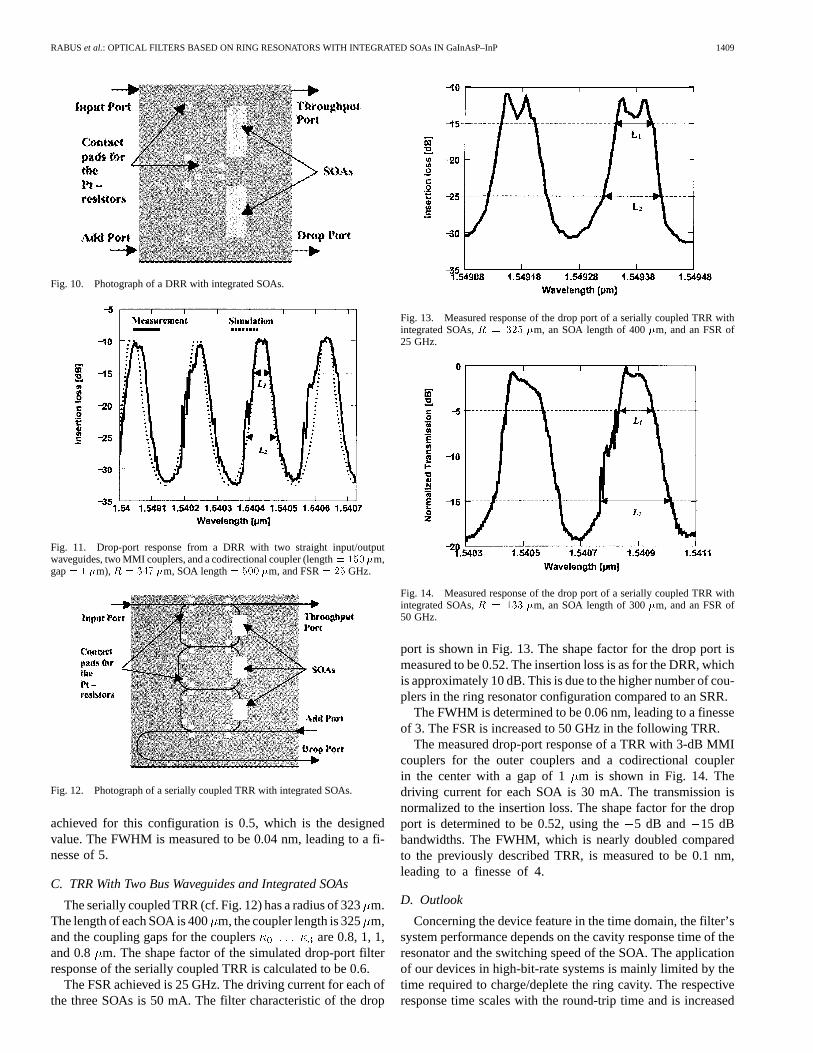
The photograph of a DRR with integrated SOAs is shownin Fig. 10. The DRR is made up of two straight input/outputwaveguides, two 3-dB MMI couplers for the outer couplers(length m, width m), and a codirectional couplerin the center (length m, gap m), m,SOA length m which results in an FSR GHz.
The measured response from the drop port is shown in Fig. 11.The driving current for each SOA is 50 mA. The shape factor
RABUS et al.: OPTICAL FILTERS BASED ON RING RESONATORS WITH INTEGRATED SOAs IN GaInAsP–InP 1409
Fig. 10. Photograph of a DRR with integrated SOAs.
Fig. 11. Drop-port response from a DRR with two straight input/outputwaveguides, two MMI couplers, and a codirectional coupler (length= 150�m,gap= 1 �m),R = 347 �m, SOA length= 500 �m, and FSR= 25 GHz.
Fig. 12. Photograph of a serially coupled TRR with integrated SOAs.
achieved for this configuration is 0.5, which is the designedvalue. The FWHM is measured to be 0.04 nm, leading to a fi-nesse of 5.
C. TRR With Two Bus Waveguides and Integrated SOAs
The serially coupled TRR (cf. Fig. 12) has a radius of 323m.The length of each SOA is 400m, the coupler length is 325m,and the coupling gaps for the couplers are 0.8, 1, 1,and 0.8 m. The shape factor of the simulated drop-port filterresponse of the serially coupled TRR is calculated to be 0.6.
The FSR achieved is 25 GHz. The driving current for each ofthe three SOAs is 50 mA. The filter characteristic of the drop
Fig. 13. Measured response of the drop port of a serially coupled TRR withintegrated SOAs,R = 325 �m, an SOA length of 400�m, and an FSR of25 GHz.
Fig. 14. Measured response of the drop port of a serially coupled TRR withintegrated SOAs,R = 133 �m, an SOA length of 300�m, and an FSR of50 GHz.
port is shown in Fig. 13. The shape factor for the drop port ismeasured to be 0.52. The insertion loss is as for the DRR, whichis approximately 10 dB. This is due to the higher number of cou-plers in the ring resonator configuration compared to an SRR.
The FWHM is determined to be 0.06 nm, leading to a finesseof 3. The FSR is increased to 50 GHz in the following TRR.
The measured drop-port response of a TRR with 3-dB MMIcouplers for the outer couplers and a codirectional couplerin the center with a gap of 1m is shown in Fig. 14. Thedriving current for each SOA is 30 mA. The transmission isnormalized to the insertion loss. The shape factor for the dropport is determined to be 0.52, using the5 dB and 15 dBbandwidths. The FWHM, which is nearly doubled comparedto the previously described TRR, is measured to be 0.1 nm,leading to a finesse of 4.
D. Outlook
Concerning the device feature in the time domain, the filter’ssystem performance depends on the cavity response time of theresonator and the switching speed of the SOA. The applicationof our devices in high-bit-rate systems is mainly limited by thetime required to charge/deplete the ring cavity. The respectiveresponse time scales with the round-trip time and is increased

1410 IEEE JOURNAL OF SELECTED TOPICS IN QUANTUM ELECTRONICS, VOL. 8, NO. 6, NOVEMBER/DECEMBER 2002
by lowering the power coupling factor. So far, the responseis characterized in the wavelength domain. System experimentsincluding dispersion measurements will be performed in a fol-lowing step. The implementation of SOAs in ring resonatorsopens the door to a wide range of active and passive devices.
The FSR of the fabricated devices can be increased in mul-tiple coupled ring resonators owing to the Vernier effect [21],[22].
V. CONCLUSION
We have demonstrated optical multistage filters usingloss-compensated ring resonator configurations with inte-grated SOAs, MMI couplers, and codirectional couplers forperforming well-specified coupling conditions between theresonators. FSRs of 12.5, 25, and 50 GHz andON–OFF ratiosfor the drop port of 20 dB for the serially coupled ringresonators have been achieved.
Accurate variation of the interresonator coupling strengthmodified the filter passband shape and demonstrated theexpected flattened response. Exemplary designs were given toachieve a specific shape factor for the drop port for the double-and triple-ring resonator configurations using appropriatecoupling factors.
The GaInAsP material system facilitates the integration of ac-tive elements like SOAs which are essential for realizing thistype of optical filter with the demonstrated filter response. Theuse of multiple coupled ring resonators provides additional de-sign flexibility to achieve various filter responses.
ACKNOWLEDGMENT
The authors would like to thank R. Steingrüber andC. Weimann (mask fabrication), H. Schroeter-Janssen(SA-MOVPE), F. Reier and H. Barsch (epitaxy), I. Tiedke,Ch. Schultz, and B. Reinsperger (photolithography), andR. Schmidt and R. Tuerck (antireflection coating). D. G.Rabus would like to thank K. Petermann, H. G. Weber, andH. Venghaus for fruitful discussions and their support.
REFERENCES
[1] E. A. J. Marcatili, “Bends in optical dielectric guides,”Bell Syst. Tech.J., vol. 48, pp. 2103–2132, 1969.
[2] B. E. Little, S. T. Chu, H. A. Haus, J. Foresi, and J.-P. Laine, “Microringresonator channel dropping filters,”J. Lightwave Technol., vol. 15, pp.998–1005, June 1997.
[3] Y. Kokubun, T. Kato, and S. T. Chu, “Box-Like response of microringresonator filter by stacked double-ring geometry,”IEICE Trans. Elec-tron., vol. E85-C, no. 4, pp. 1018–1024, Apr. 2002.
[4] Y. Ma, S. H. Chang, S. S. Chang, and S. T. Chu, “Improved opticalfilter responses in cascaded InGaAsP/InP microdisk resonators,”Elec-tron. Lett., vol. 37, no. 9, Apr. 2001.
[5] U. Troppenz, M. Hamacher, D. G. Rabus, and H. Heidrich, “All-activeGaInAsP/InP ring cavities for widespread functionalities in the wave-length domain,” inProc. Int. Conf. Indium Phosphide and Related Ma-terials (IPRM’02), Stockholm, Sweden, May 2002, pp. 475–478.
[6] B. Liu, A. Shakouri, and J. E. Bowers, “Wide tunable double ringresonator coupled lasers,”IEEE Photon. Technol. Lett., vol. 14, pp.600–602, May 2002.
[7] I.-L. Gheorma and R. M. Osgood, “Fundamental limitations of opticalresonator based high-speed EO modulators,”IEEE Photon. Technol.Lett., vol. 14, pp. 795–797, June 2002.
[8] P. Rabiei, W. H. Steier, C. Zhang, and L. R. Dalton, “Polymer micro-ringfilters and modulators,”J. Lightwave Technol., to be published.
[9] K. Djordjev, S.-J. Choi, S.-J. Choi, and P. D. Dapkus, “Vertically coupledInP microdisk switching devices with electroabsorptive active regions,”IEEE Photon. Technol. Lett., vol. 14, pp. 1115–1117, Aug. 2002.
[10] R. W. Boyd and J. E. Heebner, “Sensitive disk resonator photonicbiosensor,”Appl. Opt., vol. 40, no. 31, pp. 5742–5747, Nov. 2001.
[11] C. K. Madsen, E. J. Laskowski, L. Stulz, A. Griffin, M. A. Cappuzzo, L.Gomez, R. Long, J. Bailey, J. Weld, and P. Oswald, “An integrated po-larization mode dispersion emulator or compensator with tunable chro-matic dispersion,” inProc. Integrated Photonics Research (IPR), Van-couver, BC, Canada, July 2002, paper IthG3.
[12] J. V. Hryniewicz, P. P. Absil, B. E. Little, R. A. Wilson, and P.-T. Ho,“Higher order filter response in coupled microring resonators,”IEEEPhoton. Technol. Lett., vol. 12, pp. 320–322, Mar. 2000.
[13] K. Okamoto,Fundamentals of Optical Waveguides. New York: Aca-demic, 2000.
[14] R. Orta, P. Savi, R. Tascone, and D. Trinchero, “Synthesis of multiple-ring-resonator filters for optical systems,”IEEE Photon.Technol. Lett,vol. 7, pp. 1447–1449, Dec. 1995.
[15] G. Griffel, “Synthesis of optical filters using ring resonator arrays,”IEEE Photon. Technol. Lett., vol. 12, pp. 810–812, July 2000.
[16] D. G. Rabus, “Realization of optical filters using ring resonators withintegrated semiconductor optical amplifiers in GaInAsP/InP,” Ph.D. dis-sertation, Dept. Elect. Eng. and Comp. Sci., Technical Univ. Berlin,Berlin, Germany, 2002.
[17] D. G. Rabus and M. Hamacher, “MMI-Coupled ring resonators inGaInAsP,” IEEE Photon. Technol. Lett., vol. 13, pp. 812–814, Aug.2001.
[18] Y. Gottesman, E. V. K. Rao, B. Dagens, and S. Lovisa, “Monitoring ofmultimode imaging devices by use of optical low-coherence reflectome-ters in reflection and transmission modes,”Appl. Opt., vol. 38, no. 13,pp. 2140–2144, May 2000.
[19] D. G. Rabus, M. Hamacher, H. Heidrich, and U. Troppenz, “High-Qchannel dropping filters using ring resonators with integrated SOAs,”IEEE Photon. Technol. Lett., vol. 14, pp. 1442–1444, Oct. 2002.
[20] D. G. Rabus, M. Hamacher, and H. Heidrich, “Resonance frequencytuning of a double ring resonator on GaInAsP/Inp: Experiment and sim-ulation,” Jpn. J. Appl. Phys., pt. 1, vol. 41, no. 2B, pp. 1186–1189, Feb.2002.
[21] R. Grover, V. Van, T. A. Ibrahim, P. P. Absil, L. C. Calhoun, F. G.Johnson, J. V. Hryniewicz, and P.-T. Ho, “Parallel-cascaded semicon-ductor microring resonators for high-order and wide-FSR filters,”J.Lightwave Technol., vol. 20, pp. 900–905, May 2002.
[22] Y. Yanagase, S. Suzuki, Y. Kokubun, and S. T. Chu, “Vertical triple se-ries-coupled microring resonator filter for passband flattening and ex-pansion of free spectral range,”Jpn. J. Appl. Phys., pt. 2, vol. 41, no.2A, pp. L141–L143, Feb. 2002.
Dominik G. Rabus received the Dipl.-Ing. in elec-trical engineering from the University of Stuttgart,Stuttgart, Germany, in 1999 and Dr.-Ing. degree incomputer sciences from the Technical University ofBerlin, Berlin, Germany, in 2002.
He joined Heinrich-Hertz-Institut für Nachricht-entechnik Berlin GmbH, Berlin, Germany, in 1999,where he started his thesis on ring resonators. He iscurrently engaged in research on photonic ICs basedon InP.
Michael Hamacher received the Dipl.Ing. degree from the Nat.-Techn.Akademie of Isny in 1988.
He then joined Heinrich-Hertz-Institut für Nachrichtentechnik Berlin GmbH,Berlin, Germany, in 1988. Since then, he has been engaged in the development,fabrication, and characterization of optoelectronic/photonic integrated circuitson InP with different functionalities for future optical communication systems.

RABUS et al.: OPTICAL FILTERS BASED ON RING RESONATORS WITH INTEGRATED SOAs IN GaInAsP–InP 1411
Ute Troppenz received the Diploma Degree in physics and the Ph.D. degreefrom Humboldt University, Berlin, Germany, in 1981 and 1985, respectively.
After working at the Institutes of the Academy of Science, GDR, she hasbeen with Heinrich-Hertz-Institut für Nachrichtentechnik Berlin GmbH, Berlin,Germany, since 1992. Formerly working on electroluminescent phosphors fordisplay applications, her work is now focused on laser modeling and on thedevelopment of passive and active InP based devices for photonic ICs.
Helmut Heidrich received the Dipl. Phys andDr.-Ing. degree in physics from Technische Uni-versität Berlin, Berlin, Germany, in 1973 and 1979,respectively.
After three years work at Standard Electric LorenzAG, Berlin, he joined Heinrich-Hertz-Institut fürNachrichtentechnik Berlin GmbH (HHI), Berlin,Germany, in 1982, where for the first five years heheaded a group working in integrated optics LiNbOdevices. For over one decade, he has been engagedin research on photonic ICs (PICs) based on InP
where he was and is heading several national and European projects withinHHI on the realization of complex PICs, e.g., heterodyne receivers, opticalsweepers, bi-directional WDM-transceivers, and ps-source optoelectronic ICs.He is the author and coauthor of more than 100 publications.